

Page 1

文件编号:
版本/修订:
鴻譜數碼科技(惠州)有限公司
LSI SOLUTION DVD+RW
SERVICE MANUAL
SERVICE MANUAL
PRELIMINARY
CONFIDENTIAL
PARAMOUT DIGITAL TECHNOLOGY CO..LTD
Page 2

TABLE OF CONTENTS
TABLE OF CONTENTS
Chapter 1 Terminology and Abbreviations……………………………………………………..1-1
Chapter 2 Safety Precautions …………………………………………………………………..2-1
Chapter 3 Software Upgrade……………………………………………………………………3-1
3-1 LOADER software upgrade.…….……………………………….……….… 3-1
3-2 LSI software update. …..……………………………………………….… 3-2
Chapter 4 Electrical Performance Standards…………………………………………………...4-1
Chapter 5 Package (Inbox) and Block Diagrams ……………………………………………...5-1
Chapter 6 General Classification of Symptoms ……………………………………………….6-1
Chapter 7 Repair of Electronic Components.…………………………………………………..7-1
7-1 Repair of power board ……………………………………………………...7-1
7-2 Repair of decoding board …………………………………………………...7-5
7-3 Repair of KB board…………………………………….. …………………7-14
Chapter 8 Main-point Waveforms and Schematic Diagrams of Electronic Components
…………………………………………………………………………….……...8-1
8-1 Main-point reference waveforms of Power board ………………………….8-1
8-2 Schematic Diagrams of Power board ……………………………………….8-3
8-3 Main point reference waveforms of decoding board ……………………….8-4
8-8 Schematic Diagrams of KB board.……………………………………….8-18
Chapter 9 System decomposition 3-D diagram….……………………………………………..9-1
The BOM of the UNITS….……………………………………………. …………..9-2
8-4 Schematic Diagram of Decoding Board…………………………………….8-5
8-7 Main reference point waveforms of KB board ……………………………8-17
PRELIMINARY
CONFIDENTIAL
Page 3

Chapter 1
Terminology and Abbreviations
PRELIMINARY
CONFIDENTIAL
PRELIMINARY
CONFIDENTIAL
Page 4

Terminology & Abbreviations
Terminology & Abbreviations
AC-3 The former name of the Dolby Digital audio-coding system . AC-3 followed AC-1 and
AC-2. Still used in some standards documents.
A/V Audio/Video
Angle In DVD-video, a specific view of a scene, usually recorded from a certain camera angle.
Different angles can be chosen while viewing the scene.
ATAPI Advanced Technology Attachment (ATA) Packet Interface. An interface between a
computer and its internal peripherals such as DVD-ROM drives. ATAPI provides the
command set for controlling devices connected via an IDE interface. ATAPI is part of
the Enhanced IDE (E-IDE) interface, also known as ATA-2. ATAPI was extended for use
in DVD-ROM drives by the SFF 8090 specification.
CD Short for compact disc, an optical disc storage format developed by Philips and Sony.
CD-DA Compact disc digital audio. The original music CD format, storing audio information as
digital PCM data. Defined by the Red Book standard.
CD+G Compact disc plus graphics. A variation of CD, which embeds graphical data in with the
audio data, allowing video pictures to be displayed periodically as music is played.
Primarily used for karaoke.
CD-R An extension of the CD format allowing data to be recorded once on a disc by using
dye-sublimation technology. Defined by the Orange Book standard.
Channel A part of an audio track. Typically there is one channel allocated for each loudspeaker.
Chapter In DVD-Video, a division of a title. Technically called a part of title (PTT).
Closed Caption Text captions for video, which are not normally visible, as opposed to open
captions, which are a permanent part of the picture. In the United States, the official
NTSC Closed Caption standard requires that all TVs larger than 13 inches include
circuitry to decode and display caption information stored on line 21 of the video signal.
DVD-Video can provide closed caption data, but the sub picture format is preferred for
its versatility.
Component Video A video system containing three separate color component signals, either
red/green/blue (RGB) or chroma/color difference (YCbCr, YPbPr, YUV), in analog or
digital form. The MPEG-2 encoding system used by DVD is based on color-difference
PRELIMINARY
component digital video. Very few televisions have component video inputs.
Composite Video An analog video signal in which the luma and chroma components are
combined (by frequency multiplexing), along with sync and bu rst. Also called CVBS.
Most televisions and VCRs have composite video connectors, which are usually co lored
yellow.
Dolby Digital A perceptual coding system for audio, developed by Dolby Laboratories and
accepted as an international standard. Dolby Digital is the most common means of
encoding audio for DVD-Video and is the mandatory audio compression system for
525/60 (NTSC) discs.
Dolby Surround The standard for matrix encoding surround-sound channels in a stereo signal
by applying a set of defined mathematical functions when combining center and
surround channels with left and right channels. The center and surround channels can
then be extracted by a decoder such as a Dolby Pro Logic circuit which applies the
inverse of the mathematical functions. A Dolby Surround decoder extracts surround
CONFIDENTIAL
1-1
Page 5

Terminology & Abbreviations
channels, while a Dolby Pro Logic decoder uses tally independent of the recording or
transmission format. Both Dolby Digital and MPEG audio compression systems are
compatible with Dolby Surround audio.
DTS Digital Theater Sound. A perceptual audio-coding system developed for theaters. A
competitor to Dolby Digital and an optional audio track format for DVD-Video.
DV Digital Video. A camcorder format for high-quality video, different from PEG. It is
converted into MPEG 2 Video when recorded on DVD+RW
DVD An acronym that officially stands for nothing, but is often expanded as Digital Video
Disc or Digital Versatile Disc. The audio/video/data storage system based on 12-and
8-cm optical discs.
DVD+R
DVD+RW Discs can be written to and erased multiple times. Existing recordings can be deleted
EasyLink If your TV set and your video recorder are equipped with this feature, they can
I.LINK Also known as ‘FireWire’ and ‘IEEE 1394’. A cable fo r transfer of highbandwidth
Index Picture Screen A screen that gives an overview of a DVD+RW disc, with
JPEG Joint Photographic Experts Group. The international committee, which created its
Karaoke Literally empty orchestra. The social sensation from Japan where sufficiently
Macro vision An ant taping process that modifies a signal so that it appears unchanged on
MPEG Motion Picture Experts Group. A collection of compression systems for digital audio and
Multiangle A DVD-Video program containing multiple angles allowing different views of a
Multilanguage A DVD-Video program containing sound tracks and subtitle tracks for more than
NICAM System for reception of digital stereo TV sound.
NTSC See TV system. NTSC is the most common color system in the U.S.
OTR One-Touch Recording. With this feature you can easily start a recording (by pushing just
OSD On-screen Display. The ‘user interface’ by which you can control the DVD recorder via
These discs can only be written to once. Existing recordings can be hidden but not
deleted. So, any disc space already used by a recording cannot be regained. DVD+R
discs are required to be "Finalized" before they will be compatible with standard DVD
Players. Once a disc is finalized, no further recordings can be made.
and disc space regained. These discs do not require a finalization procedure. As soon as
a recording is made, the disc will be compatible with standard DVD Players.
exchange information to adjust certain settings to each other, such as the TV channel
order and other user preferences
digital signals, as used by Digital Video camcorders.
‘indexpictures’ that each represent a recording.
namesake standard for compressing, still images.
inebriated people embarrass themselves in public by singing along to a music track.
Karaoke was largely responsible for the success of laserdisc in Japan, thus supporting it
elsewhere.
PRELIMINARY
most televisions but is distorted and unmatchable when played back from a videotape
recording. Macro vision takes advantage of characteristics of AGC circuits and burst
decoder circuits in VCRs to interfere with the recording process.
video.
scene to selected during playback.
one language.
one button) and select the switch-off time in intervals of 30 minutes.
CONFIDENTIAL
1-2
Page 6

Terminology & Abbreviations
the TV screen.
PAL See TV system.
PBC Playback Control. A special feature on a VCD 2.0 or Super VCD disc that enables
interactive use.
PBS Public Broadcast Service. The channel that transmits data for Auto Clock Set and VCR
Plus+ programming.
PCM Pulse Code Modulation. A digital audio encoding system.
PDC Program Delivery Control
RGB Red-Green-Blue. A top-quality video connection where red, green and blue components of
a video signal are carried through separate wires.
SCART cable Also known as Euro-AV cable. This standard cable is an easy way to connect
various AV devices and televisions. In addition to audio and video it can carry
control signals.
S/N Signal-to-noise ratio. Also called SNR.
Subtitle A textual representation of the spoken audio in a video program. Subtitles are often
used with foreign languages and do not serve the same purpose as captions for the
hearing impaired.
SECAM See TV system.
ShowView See VideoPlus+. ‘ShowView’ is a trademark of Gemstar Development Group.
S-video A video interface standard that carries separate luma and chrome signals, usually on a
four-pin mini-DIN connector. Also called Y/C. The quality of s-video is significantly
System menu The main menu of a DVD-Video disc, from which titles are selected. Also called
Title The largest unit of a DVD-Video disc (other than the entire volume or side). Usually a
TruSurround A system for simulating Multi-channel sound reproduction via a two channel
TV system There are various systems for transmitting television signals, for example PAL, PAL-I,
Video CD An extension of CD based on MPEG-1 video and audio. Allows playback of
VCR PLUS+ A system by which you can easily program the TIMER of your video recorder by
VCR Video Cassette Recorder
VPS Video Programming System
YUV In the general sense, any form of color-difference video signal containing one luma and
better than composite video since it does not require a comb filter to separate the signals,
but it’s not quite as good as component video. Most high-end televisions have s-video
inputs. S-video is often erroneously called S-VHS.
the title selection menu or disc menu.
movie, TV program, music album, or so on. A disc can hold up to 99 titles, which can be
selected from the disc menu.
PRELIMINARY
set-up, by SRS Labs, Inc.
CONFIDENTIAL
PAL-BG, SECAM, SECAM-DK, NTSC, etc. The TV system is country dependant.
near-VHS-quality video on a Video CD player, CD-I player, or computer with MPEG
decoding capability.
entering a code of maximum 9 digits, which is printed in TV guides. ‘Video
Plus+’ is a trademark of Gemstar Development Group.
two chroma components. Technically, YUV is applicable only to the process of encoding
component video into composite video.
1-3
Page 7

Chapter 2
Safety Precautions
PRELIMINARY
PRELIMINARY
CONFIDENTIAL
CONFIDENTIAL
Page 8

SAFETY PRECAUTIONS
IMPORTANT SAFETY PRECAUTIONS
Prior to shipment from the factory, the products are strictly inspected to conform with
the recognized product safety and electrical codes of the countries in which they are to
be sold. However, in order to maintain such compliance, it is equally important to
implement the following precautions when a set is being serviced.
·Precautions during Servicing
1. Locations requiring special caution are denoted by labels and inscriptions on the
rear panel and certain parts of the product. When performing service, be sure to
read and comply with these and other cautionary notices appearing in the
operation and service manuals .
2. Parts identified by the symbol in schematic diagram parts are critical for safety.
Replace only with specified part numbers.
Note : Parts in this category also include those specified to comply with laser
emission standards for Products using cathode ray tubes and those specified
for compliance with various regulations regarding spurious radiation.
3. Use Specified internal wiring. Note especially:
1) Double insulated wires
2) High voltage leads
PRELIMINARY
!
CONFIDENTIAL
4. Use specified insulating materials for hazardous live parts. Note especially:
1) Insulation Tape
2) PVC tubing
3) Spacers
4) Insulation sheets for transistor
5. Observe that wires do not contact heat producing
PARTS (heat sinks, oxide metal film resistors, fusible resistors, etc.)
2-1
Page 9
SAFETY PRECAUTIONS
6.Check that replaced wires do not contact sharp edged or pointed parts.
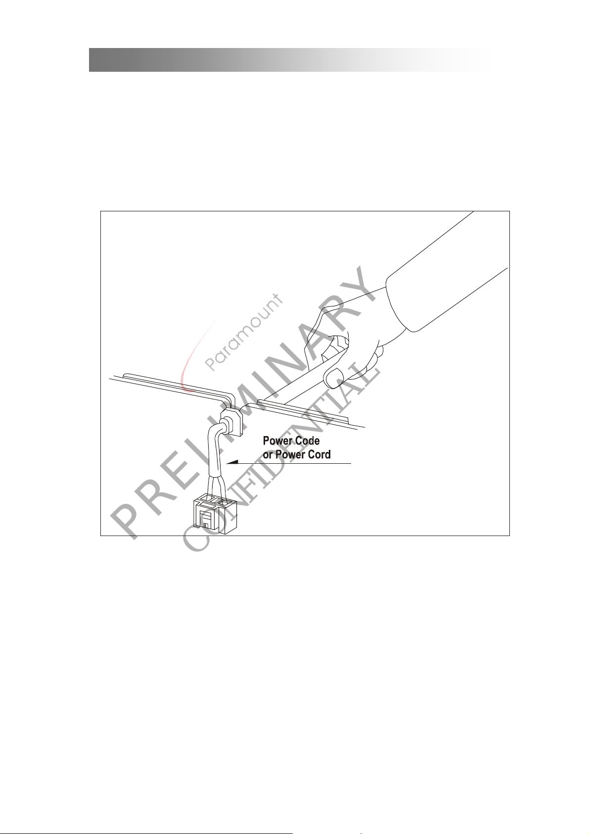
7. 1) When a power cord has been replaced, check that A mark is made on the cord,
under strain, near the aperture, and the flexible cord is subjected 100times to a
pull of 40N for a duration of 1 second each.
2) During the test, the cord shall not be displaced by more than 2mm
8.Also check areas surrounding repaired locations.
9. The internal wiring is secured so as not to approach the heating parts and high
PRELIMINARY
CONFIDENTIAL
voltage parts by its shape.
So, these wires must be restored to its former state.
10. After updated the hazardous live part or accessible part, if the clearance or creep
age distance can’t accord with the safe request, then need adopt reinforced insulation
method for ensure safety.
SAFETY CHECK AFTER SERVICING
Examine the area surrounding the repaired location for damage or deterioration.
2-2
Page 10
SAFETY PRECAUTIONS
Observe that screws, parts and wires have been returned to original positions.
Afterwards, perform the following tests and confirm the specified values in order to
verify compliance with safety standards.
·Insulation resistance test
Confirm the specified insulation resistance or greater between power cord plug prongs
and externally exposed parts of the set (RF terminals, antenna terminals, video and
audio input and output terminals, microphone jacks, earphone jacks, etc.) See table
below.
·Dielectric strength test
Confirm specified dielectric strength or greater between power cord prongs and
exposed accessible parts of the set (RF terminals, antenna terminals, video and audio
input and output terminals, microphone jacks, earphone jacks, etc.) See table below.
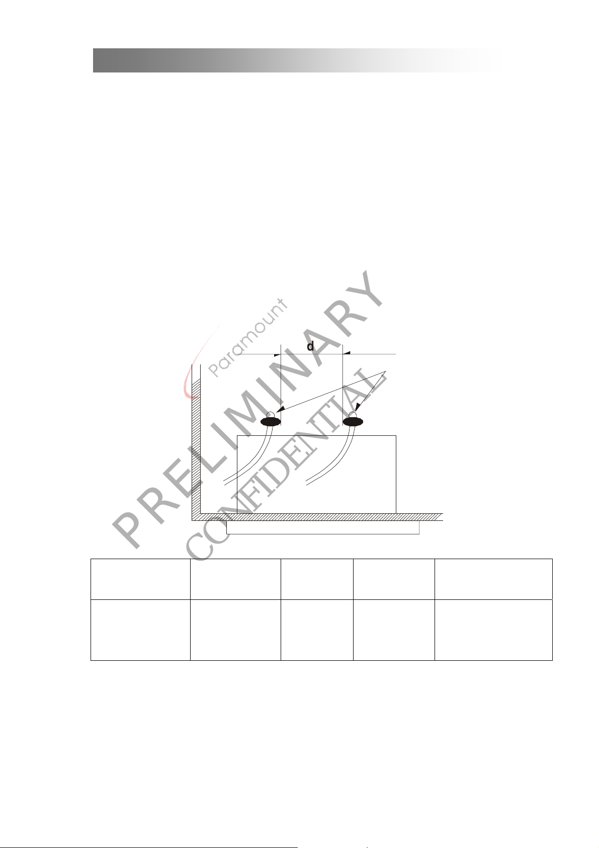
·Clearance distance
When replacing primary circuit components, confirm specified clearance distance (d),
between soldered terminals, and between terminals and surrounding metallic
parts .See table below.
Table 1: Ratings for selected areas
AC Line Voltage Region
PRELIMINARY
*110 to 240 v
110 to 230 v
CONFIDENTIAL
USA, Australia
Europe
Insulation
Resistance
F
4M/500VD
C
Dielectric
Strength
4kv/minute F 6mm(d)
Clearance
Distance(d),(d)
*Class ll model only.
Note. This table is unofficial and for reference only. Be sure to confirm the precise
values for your particular country and locality.
· Leakage Current test
Confirm specified or lower leakage current between B (earth ground, power cord plug
2-3
Page 11
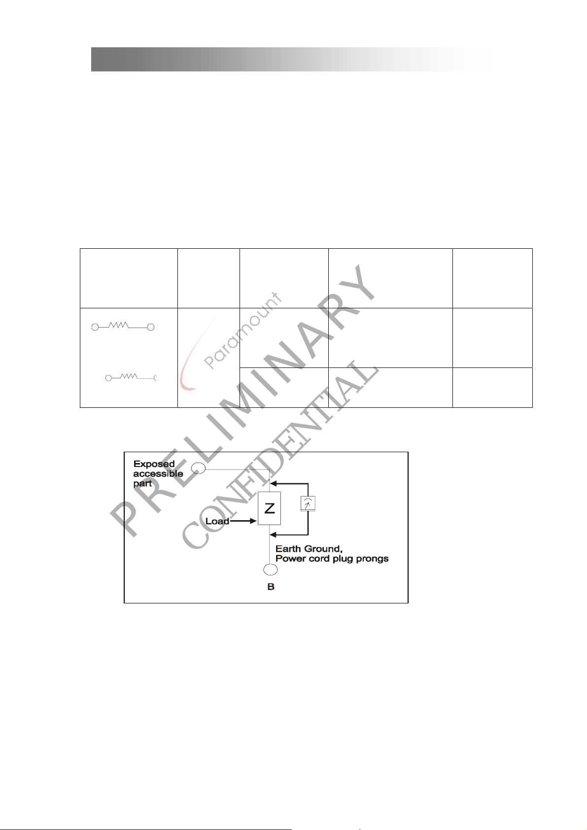
m
SAFETY PRECAUTIONS
prongs) and externally exposed accessible (RF terminals, antenna terminals, video and
audio input and output terminals, microphone jacks, earphone jacks, etc.)
Measuring Method: (Power ON)
Insert load Z between B (earth ground, power cord plug prongs) and exposed
accessible parts .Use an AC voltmeter to measure across both terminals of load Z. See
figure and following table.
Table 2: Leakage current ratings for selected areas.
Leakage Current
Earth
AC Line Voltage
Region Load Z
(i)
Ground
(B) To:
Antenna
2k ohm
100 to 130 v
Europe
<Or= 0.7mA peak
earth
<Or= 2mA DC
Terminals
200 to 240 v
50k oh
Note. This table is for IEC member only. Be sur e to confirm the precise values for
your particular country and locality.
PRELIMINARY
Australia
<Or=0.7mA peak
<Or= 2mA DC
CONFIDENTIAL
Other
terminals
2-4
Page 12

Chapter 3
Software Upgrade
PRELIMINARY
PRELIMINARY
CONFIDENTIAL
CONFIDENTIAL
Page 13

Software update
1、 RW loader upgrade solution
1 How to make CD-R download disc for DRL-200.
a) Please add attached the file to be download (extension of the file name is CVT) to a blank
CD-R
CD-R downl oad disc should have only 1 file to be downloading , so you must add no other
files to CD-R Disc.
Set Recording Options as followings.
File Format (or Mode): CD-ROM Mode 1 format.
File System: ISO Level 2, Length of file name exceeds 8 (so Max 31 or Higher)
b) Please type the volume name of the CD-R/RW as "ATPLDR_DOWN" exactly.
The volume name is not case-sensitive.
c) When you are ready to make a CD-R download disc, you should make CD-R session
closed.
That is, CD-R download disc must be a single session disc.
2 The downloading procedure with CD-R download disc is as below.
a) Please power on your set without any disc.
b) Please eject the tray after confirming "No disc".
c) Please insert the download CD-R. Downloading program will be started automatically.
After DRL-100 reads all of the code to be downloaded, Tray is automatically opened.
c) Please remove the download CD-R and don’t close the Tray.
d) Writing the code to flash memory will be progressed.
e) Please certainly wait until tray closed of itself. Maybe it takes about 1 minute to end the
downloading.
f) If the tray is closed automatically, Download is successful,
Or if the tray is not closed automatically in several minutes, Download is failed.
PRELIMINARY
g) If success, please power off and on to reset it.
CONFIDENTIAL
3-1
Page 14
LSI software upgrade
2. LSI+ATAPI (DMN8600/DMN8602) upgrade solution
1 How to make CD-R download disc for DMN8600/DMN8602
a) Please add attached the file to be download (extension of the file name is dmn8600.cub) to
a blank CD-R
CD-R downl oad disc should have only 1 file to be downloading , so you must add no other
files to CD-R Disc.
b) When you are ready to make a CD-R download disc, you should make CD-R session
closed.
That is, CD-R download disc must be a single session disc.
2 The downloading procedure with CD-R download disc is as below.
1) Please power on your set without any disc.
2) Please eject the tray.
3) Please insert the download CD-R. Downloading program will be started automatically.
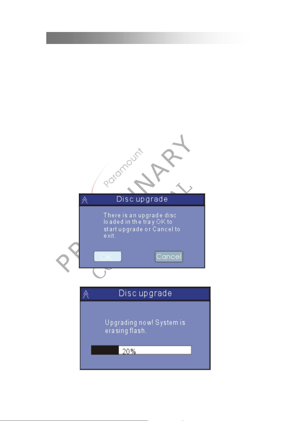
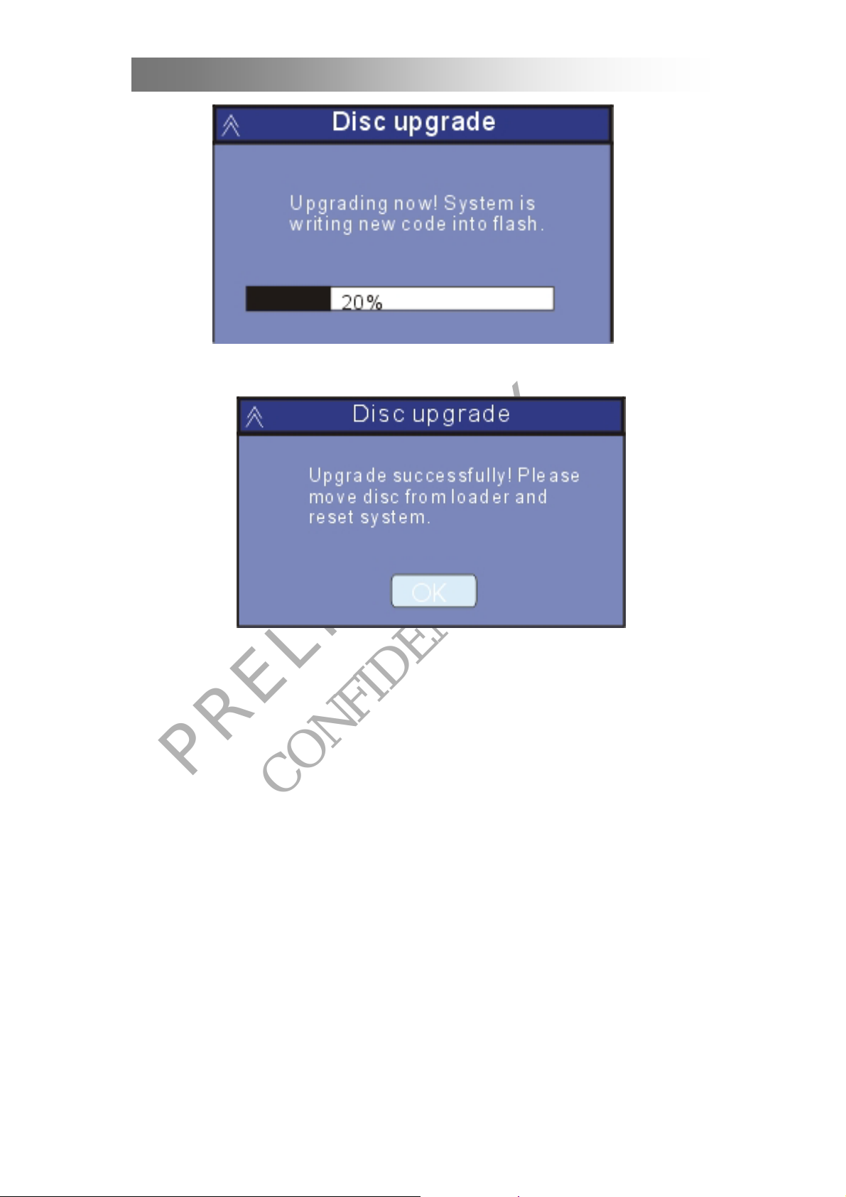
a) After RW Loader reads the DMN8600 upgrade disc, the disc upgrade menu as blow
will be displayed on TV screen.
PRELIMINARY
b) Select Cancel to quit upgrade and the tray will auto open. Select OK to start upgrade,
then the disc upgrade menu will be changed..
CONFIDENTIAL
3-2
Page 15
LSI software upgrade
b) After select OK to start upgrade, System will erase and Write the code to flash memory.
The schedule will indicate upgrade progressed status.
c) Aft er upgrade successfully, VFD will display FINISH character and TV will display the
Upgrade successfully menu. Then the tray is automatically opened, Please remove the
download CD-R,
d) Please select Ok to reset it. If can’t software reset, please power off and restart it.
Notes: A. If the upgrade menu display that upgrade failed, it perhaps the upgrade disc not be
PRELIMINARY
recorded successfully. Please make download disc again.
B. During upgrading, the RECORDER machine could not be operated;
C. If there is no picture, no sound after restarting, this is a hang-up during upgrading.
At this stage, the RECORDER machine could not be functional and a correct procedure of
FLASHMEMORY has to be replaced.
CONFIDENTIAL
3-3
Page 16

Chapter 4
Electrical Performance Standards
PRELIMINARY
CONFIDENTIAL
Page 17
Electrical Performance Standards
KEY PERFORMANCE LIST
ITEM TEST CONTENT UNIT SPECIFICATION
1 ANALOG OUTPUT LEVEL
2
A
U
3
D
I
O
4
5 THD+N dB ≤-60(1KHz)
6 CROSS-TALK dB ≥70
7 CHANNEL DIFFERENCE dB ≤1.5
C
H
A
R
A
C
8
T
E
R
9
10
11
12
13
14
15
V
I
D
E
16
PRELIMINARY
CHARACTER
17
18
O
COAXIAL OUTPUT LEVEL
20Hz dB ±2
125Hz dB ±2
FREQUENCY
RESPONSE
S/N RATIO(A-WTD) dB ≥90
LEVEL
NON-
LINEAR
DYNAMIC RANGE dB ≥75(1KHz)
DIGITAL OUTPUTLEVEL (Vp-p)LOAD 0.5±0.05
VIDEO OUTPUT LEVET Vp-p 1.0±0.2
R(red) channel output level
G(green) channel output level (Vp-p) LOAD 0.7±0.14
B(blue) channel output level
HORIZONTAL DEFINITION
LUMINANCE CHNANEL
BANDWITH
LUMINANCE NON-LINEAR
CONFIDENTIAL
DISTOR TION
DIFFERENTIAL PHASE DP( 0 ) ≤8
OUTPUT LEVEL (Vp-p) LOAD 1.5±0.5
1KHz dB ±2
18KHz dB ±2
20KHz dB ±2
0
-10
-20
-40
-60
(V)10k LOAD
Vp-p 0.9±0.1
dB
(Vp-p) LOAD 0.7±0.14
(Vp-p) LOAD 0.7±0.14
LINE ≥500
MHz ≥3.5
% ≤2
1.7±0.3
±3
DISTORTION % ≤0.5
19
MIC
CHARACTER
20
21 S-VIDEO LUMINANCE LEVEL (Vp-p) LOAD 0.7±0.14
22 S-VIDEO COLOUR SYNCH LEVEL (VP-P)LOAD 0.3±0.06
OTHERS
FREQUENCY RESPONSE
(120Hz/5K)
S/N RATIO dB ≥45
REDING TIME S ≤5
LONG TIME READ TIME S ≤10
MAX POWER CONSUMER VA or W 30
4-1
dB ±3
Page 18

Chapter 5
Package (Inbox) and Block Diagrams
PRELIMINARY
CONFIDENTIAL
Page 19
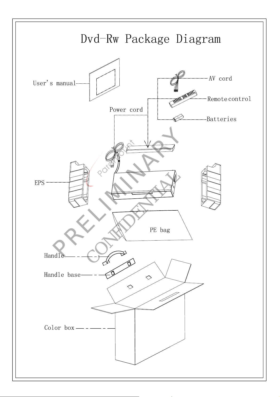
PRELIMINARY
CONFIDENTIAL
Page 20
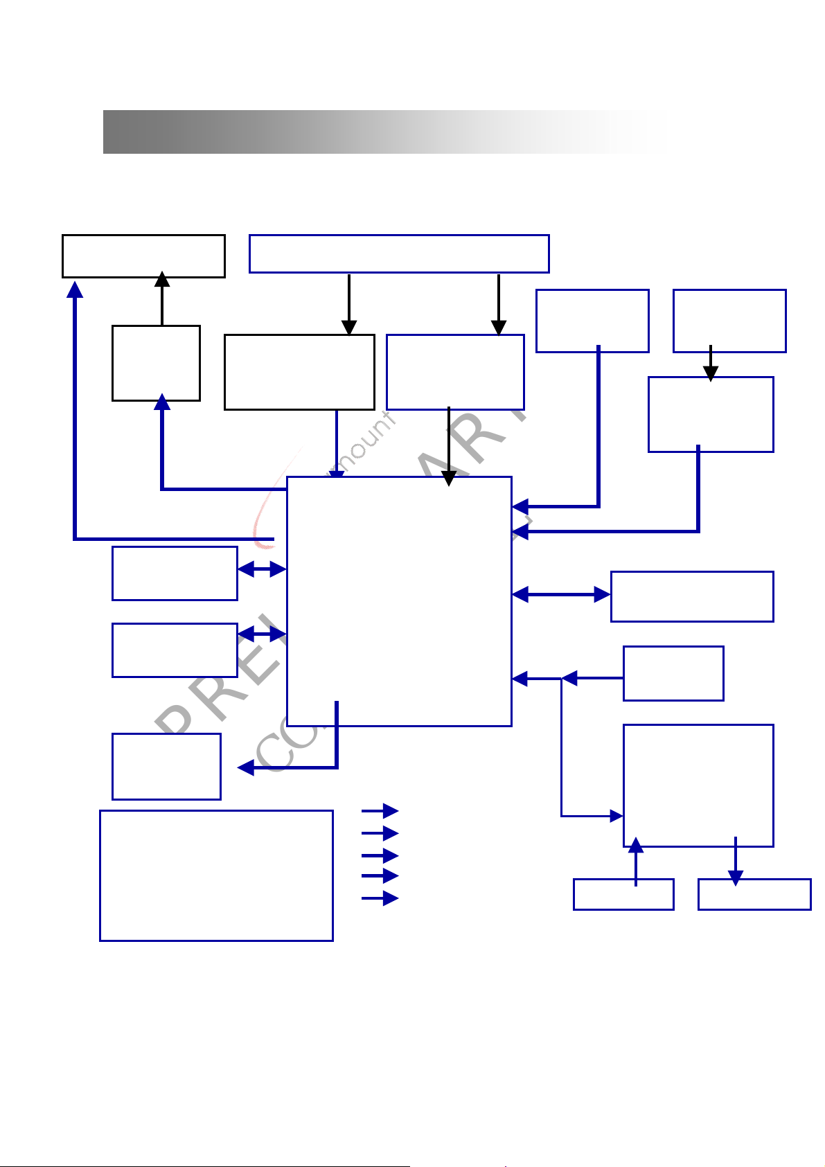
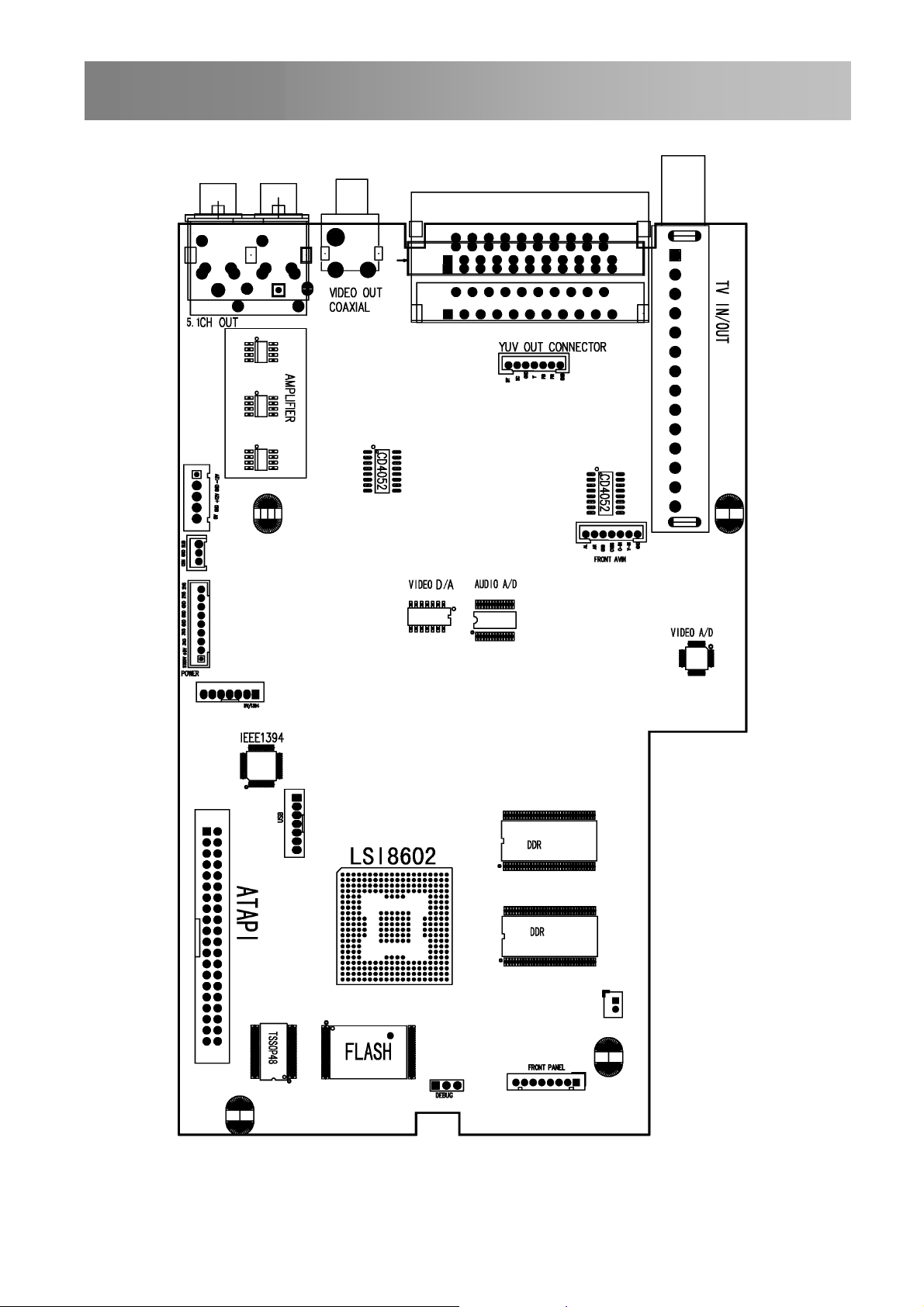
Circuit Block Diagram
AV OUT PORT
CS4360
AUDIO D/A
CONVERTOR
VIDEO OUTPUT
DDR SDRAM
(64 Mbit )
DDR SDRAM
(64 Mbit )
DVD+RW
PRELIMINARY
LOADER
POWER REG
AV INPUT PORT and TV TUNER
USB INPUTP
PORT
PCM1801
AUDIO A/D
CONVERTOR
5150
VIDEO ADC
MN8602 Chip
ENCODER/DECODER
System Controller
Buffer Memory Controller
CONFIDENTIAL
+5V
+3.3V
+2.5V
+12V
-12V
-
DV INPUTP
PORT
TSB41AB1
(1394 PHY )
FLASH MEMORY
(16 Mbit )
IR
receiver
EPV6200
VFD DRIVER
RTC
AND KEY MATRIX
SCAN
LED DISPLAYKEY MATRIX
Page 21
Power Board Block Diagram
Power board block diagram
PRELIMINARY
C2
CON4CON8
D12 D15
T1
CONFIDENTIAL
CON5 CON6
5-3
CON7
L1
F1
CON2 CON3
TL431
CON1
C6
EPC817
IC2
365
C1
Page 22
Decoder Board Block Diagram
PRELIMINARY
CONFIDENTIAL
5-4
Page 23

PRELIMINARY
CONFIDENTIAL
Page 24

Chapter 6
General Classification of Symptoms
PRELIMINARY
CONFIDENTIAL
Page 25

N
N
N
N
t
d
N
N
N
N
N
f
f
N
t
General Classification of Symptoms
d
N
N
Chapter 6
General Classification of Symptoms
Class I:
o Display on VFD
Check whether the POWER cord is
connected well with the core o
decoding board?
Is it normal after correc
re-connection?
well with the power board and KEYboard?
Y
Check whether the wire is
connected well with the deco ding
board and KEYboard?
Y
Y
Is it normal after correct re-connection?
Is it normal after correct re-connection? Check whether the power cord is connecte
To repair flowchart of KB board K1
Class II:
Is the KB board OK?
Y
o Sound from TV
To repair flowchart of decoding board D1
To power board repair
PRELIMINARY
Check whether the audio cords
between the RW machine and the
CONFIDENTIAL
TV are connected correctly?
The right and left channels outpu
terminals of the machine are connecte
with the TV audio input termina l
Y
Are the SCART cords between the
machine and TV connected correctly?
Re-connect correctly
Y
Is the audio setting up o
the machine correct?
Y
Set up correctly according to the instruction manual
Page 26

N
N
N
p
N
NYN
N
N
N
N
N
t
W
b
d
y
N
N
d
g
General Classification of Symptoms
Class III:
o display on TV
6-1
Check whether the vid eo cords between th e R
machine and TV are connected correctly?
The video output terminal of the
machine is connected with TV video
in
ut terminal
Are the SCART cords
etween the machine an
Is it normal after correct re-connection?
Y
Is the video setting up of the machine correct?
Is it normal when it is set up correctl
according to instruction manual?
Y
Check whether the wire is co nnected well between
the decoding board
Is it normal after correct re-connection?
Y
Check whether the ATTPI (fla
type) is connected well with the
decoding board and RW loader
PRELIMINARY
To repair flowchart of decoding board
Y
CONFIDENTIAL
Is it normal after correct re-connection?
Class IV:
The door of tray does not open
Is the door wedging the core in?
Y
Adjust the position of the core
Check whether the ATAPI cor
is connected well with the co re
of decodin
board?
Y
Is it normal after correct re-connection?
Ⅱ
Ⅰ
6-2
Page 27

N
N
N
N N
NY N
g
n
m
n
h
t
Y
N
N
General Classification of Symptoms
Check whether the core, load er and the
decodin
When pressing the “open/cl ose” butto
on front panel, is there any wavefor
on the SO cord of KB board (PIN 4)?
When pressing the “open/close” button on
remote control, is ther e any waveform o
the SO cord of KB board (PIN 4)?
Class V:
Replace RW loader
Is the disc scratched or dirty?
PRELIMINARY
CONFIDENTIAL
Check whether the ATAPI
cord is connected well wit
the core of decoding board?
Check whether the wire (fla
type) is connected well with the
decoding board and RW loader?
Replace RW loader
Ⅰ
board are connected?
Y
Y
Disc cannot be read
Y
Ⅱ
Is it normal after correct re-connection?
To repair flowchart of KB board K3
To repair flowchart of KB board K2
To repair flowchart of decoding board
Y
Change the disc
Is it normal after correct re-connection?
Is it normal after correct re-connection?
6-3
Page 28

N
N
N
General Classification of Symptoms
Class VI:
Class VII:
Class VIII:
PRELIMINARY
Abnormal output from coaxial
Picture/sound distorted
Y
Is the disc scratched or dirty?
To repair flowchart of decoding board
Check whether the connecti on between
the external decoding system and the
optical fiber/coaxial is OK?
Y
To repair flowchart of decoding
board
Disc reading stops
Replace the disc
Set up correctly according to
instruction manual
CONFIDENTIAL
Y
Is the disc scratched or dirty?
Replace RW loader
Replace the disc
6-4
Page 29

General Classification of Symptoms
N N
N
N
h
t
Class IX:
Class X:
Class XI:
PRELIMINARY
Hang up while reading disc
Replace RW loader
Remote control does not operate normally
To repair flowchart of KB board K2
Hang up while recording disc
Is the disc scratched or dirty?
Check whether the ATAPI
cord is connected well wit
the core of decoding board?
Y
Check whether the wire (fla
type) is connected well with the
CONFIDENTIAL
decoding board and RW loader ?
Y
Replace RW loader
Replace the disc
Is it normal after correct re-connection?
Is it normal after correct re-connection?
To repair flowchart of decoding
board
6-5
Page 30

N N
NY N
h
t
N
N
d
d
N
N
h
General Classification of Symptoms
Class XII:
Class XIII:
PRELIMINARY
Hang up while closing disc
Is the disc scratched or dirty?
Y
Check whether the ATAPI
cord is connected well wit
the core of decoding board?
Replace the disc
Is it normal after correct re-connection?
Check whether the wire (fla
type) is connected well with the
decoding board and RW loader ?
Is it normal after correct re-connection?
Y
Replace RW loader
Select recording source NO display on TV
Check whether the video cords between
the RW machine and source machine are
connected correctly?
CONFIDENTIAL
Y
To repair flowchart of decoding
board
The video output terminal of the
SOURCE machine is connected wit
machine video input terminal
Check whether the wire is connecte
well between the AV OUT boar
and decoding board
Is it normal after correct re-connection?
Y
To repair flowchart of decoding board
6-6
Page 31

N
N
d
N
h
N
N
f
General Classification of Symptoms
Class XIIII:
Class XIV:
PRELIMINARY
Select recording source NO sound on output
Check whether the audio cords between
the RW machine and source machine are
connected correctly?
Check whether the wire is connecte
well between the decoding board
Y
To test flow chart of decoding board
Playback mosaic after record
Is the disc scratched or dirty?
Check whether the source
CONFIDENTIAL
video is normal?
Replace RW loader
Y
Y
Y
The audio output terminal of the
SOURCE machine is connected wit
machine audio input terminal
Is it normal after correct re-connection?
Replace the disc
To repair or replace machine o
source
6-7
Page 32

Chapter 7
Repair of Electronic Components.
PRELIMINARY
CONFIDENTIAL
PRELIMINARY
CONFIDENTIAL
Page 33

Repair of Electronic Components
7-1 Repair of Power Board
I. Power switch working principles
The internal parts of main power switch IC 2A365 (IC2) consist of: oscillation circuit,
error test and T-ratio over current overheating protection, under-voltage and over voltage
protection, and power-amp MOSFET. For descriptions of pins and block diagrams of internal
IC, see appendix.
1. Conversion from AC. to DC. circuit
230V/110V AC. current flows restrictively through F1 fuse, L1 and C1,C6,C7
combines to be share-mode and differential-mode filter circuit, filtering external
disturbance and preventing internal electromagnetic radiation, and through
D1~D2 and D5~D6 to combine as bridge rectification. After C2 undergoes
electrolytic filter, we can obtain a 320/140V DC. voltage (Uhv).
2. Process to start up the software
Connect R3, R8 to the multi-functional VCC pin of IC2, test DC. input voltage Uhv.
This can effect as a protective function to restrict under-voltage current and reduce over
voltage T-ratio.
C44 and C24 are the charging circuits to start up software, and electric current
inside IC flows from control pin 1. When Vc reaches 5.3V, internal oscillation circuit
initiates, motivating power-amp MOSFET, forming AC. current on T1 P1~P3 primary
T ratio will increase (or decrease) and the output voltage will increase (or decrease).
winding, coupling to secondary winding. Power switch start-up has completed.
3. Bias winding
After starting the power, T1 P5~P6 bias winding supplies bias current and error
current to pin7l of IC2, through D10 and C13 rectifier filter .
4. Clamping protective circuit
C3, R2, D8 are connected to primary switch transformer, in order to fix the leakage
electrode voltage of IC2 and to prevent the voltage exceeding the limit of IC2 leakage
electrode voltage when switch transformer discharges at startup or overloading stage.
PRELIMINARY
5. Regulation process of output voltage
When the input current of control pin (FB) IC2 decreases (or increases), oscillation waveform will be regulated automatically so that
Output voltage feedback circuit is completed by Q5, U3.
Q5 (TL431) is a reference regulation IC, reference voltage is 2.5V:
Its pins are shown on the diagram below:
CONFIDENTIAL
7-1
Page 34

Repair of Electronic Components
Main characteristics of TL431
(1) anode voltage Vka, anode change in voltage
(2) reference voltage, reference change in voltage
Secondary main winding, set 5V to output change in voltage△Vo; we can
deduce △V
From this formula we can deduce: If 5V Voltage rises, the voltage V
two ends of R25 will rise, error voltage increases by 356 times. V
voltage is added to the light-emitting diode of U3 optical coupling, so that the
emitting intensity increases. Coupling increases the current of U3 light-electric
triode. The control current of IC2 then rises and the T ratio of open/close power
reduces, thus reducing 5V output voltage.
On the other hand, if 5V voltage reduces, negative feedback will cause it
to rise automatically.
6. Output voltage for the first time
After 5V main feedback winding has been regulated, other windings will
be regulated relatively, and the voltage required by each circuit of the
RECORDER machine can be obtained.
it is damaged, the VFD cannot be lightened up.
II. Repair flowchart of open/close power:
Below are two flowcharts for troubleshooting which occur frequently when open/close power
among the open/close waveforms (the other half cycle voltage rises when the
input voltage rises), and the open/close frequency is as high as 130KHz,
so that all secondary class uses rectification.
Repair of Power Board
PRELIMINARY
=356△Vo
R305
of the
R25
error
R25
D3 provides a ground impedance bias voltage to filament voltage. When
Since there are only half of the cycle which is useful for regulation
CONFIDENTIAL
7-2
Page 35

n
r
N
N
N
N
Repair of Electronic Components
1.
No voltage output
Measure each output terminal to
see whether it is short circuit
O
Measure the voltage of C2
About 320V/140
Measure the voltage of 5pin (Drain)
of IC2
About 320V/140
Measure whether the voltage of 7
pin IC2 (VCC) is equal to8.5V
O
Measure whether the voltage of 2
pin IC2 (M) is equal to 5.3V
O
Test whether the windings of T1 are
short circuit, open circuit
O
Measure other elements
PRELIMINARY
CONFIDENTIAL
YES
Far less than 320V/140
0V
YES
YES
YES
Eliminate short-circuit point
Check AC. and DC. conversio
elements such as FUSE, powe
switch, L1, D1,D2,D5,D6 etc.
Open circuit of 1~3 pins of T1
R3, R8 or IC2 are damaged
Check whether R19, C25 or U3 are
damaged
Replace T1
7-3
Page 36

t
f
N
N
N
No N
N
N
Repair of Electronic Components
1. 2.Unstable voltage output, decrease of carrier capability
Take out the output cord, connec
ormal output voltage
Abnormal
Measure the working temperature o
elements by infrared thermometer
ormal
Abnormal
Is the voltage of light-emitting tubes in
optical coupling at about 1V?
Yes
o
Is the reference voltage of Q5 at
2.5V?
Yes
Is the voltage of IC2 control pin
normal?
Yes
Is the voltage of C2 at 320V/140?
Yes
o
o
Test other elements
PRELIMINARY
CONFIDENTIAL
Other power boards overloaded
Analyze heating elements
Replace optical coupling
Is it normal after replacing TL431?
o
CheckR19,C25 or IC2
There is damage in D1,D2,D5,D6
forming half-wave rectification
7-4
Page 37

N
Repair of LSI8602 Decoding Board
N
N
p
p
N
NO N
7-2 Repair of Decoding Board
D1
D2 Remote control does not function
D3 Buttons does not function
PRELIMINARY
o display on VFD
YES
Is the JP1 socket loose?
O
Is the JP2 socket loose?
YES
Repair Key board
Is control on standby mode? Is the JP2 soket loose?
YES
Replace DMN8602
Is control on standby mode ? Is the JP2 soket loose?
Check R49 R50 R51 R52 R53
deteriorated
Replace DMN8602
CONFIDENTIAL
YES
YES
O YES
Insert the JP1 plug tightly
Insert the JP2 plug tightly
Replace Key board
O
Replace Key board
7-5
YES
Insert the JP2
lug tightly
YES
O
YES
Insert the JP2
lug tightly
Replace R49 R50
R51 R52 R53
Page 38

Repair of LSI8602 Decoding Board
N
f
d
NO N
y
N
R
N
D4 Disc can’t read
D5
Is the CN1 plug loose?
O
Check whether RW LOADE
has deterionated Repcace LOADER
YES
Replace DMN8602
o display, N o sound from TV
Is AV board + 12V, -12V 5V power suppl
normal?
Is decoding board +3.3V, 2.5V
1.8V power supply normal?
PRELIMINARY
Is the replacement circu it o
CONFIDENTIAL
DMN8602 normal?
Is DDR SDRAM(U4,U5) communications
normal?
Replace DMN8602
YES
O
O
YES
YES
Insert the CN1 plug tightly
YES
Repair POWER board
YES
Check the power circuit consisting
of U11,U12,U15
YES
Check U1(DMN8602) an
external circuit
YES
Check DDR SDRAM circuit
7-6
Page 39

N
N
plug
y
V
NO N
N
V
N
N
Repair of LSI8602 Decoding Board
D6
There is display but no sound on the TV
Check whether U26(CS4360)
Output waveforms normal
YES
Repcace IC U26(CS4360)
Check whether U22(CD4052)
Output waveforms normal
O
YES
Repcace IC U22(CS4052)
O
Check whether U24 U25 U27
(JRC4558DR)Output waveforms normal
O
YES
Repcace IC U24 U25 U27
deteriorated
Check whether A
cable to RCA loose
YES
Insert the AV cable to
RCA plug tightly
D7
o display on the TV(SCART YUV S-VIDEO or composite video output) , normal sound
SCART YUV S-VIDE CVBS
whether Output are normal
YES
Repair IC U2(L5150)
PRELIMINARY
Check whether L8-L19
CONFIDENTIAL
someone deteriorated
O
YES
Replace L8-L19 deteriorated
Check whether Q15 Q16 Q17
Q18 Q19 Q23 Q26 Q27 Q34
someone deteriorated
O
YES
Replace Q15 Q16 Q17 Q18
Q19 Q23 Q26 Q27 Q34
deteriorated
Check whether A
cable to RCA loose
YES
Insert the AV cable to
RCA
tightl
7-7
Page 40

y
Repair of LSI8602 Decoding Board
N
N
N
N
y
t
N
N
N
D8
Picture distorted
Is U1(DMN8602) power suppl
circuit normal
YES
O
Repair power supply circuit
Is U1(DMN8602) and communications
normal?( L8-L19)
O
Repair communication circuit
YES
Check whether Q15 Q16 Q17 Q18 Q19
Q23 Q26 Q27 Q34 normal?
YES
Replace Q15 Q16 Q17 Q18 Q19 Q23 Q26
Q27 Q34 deteriorated
O
Check whether R558 R562 R564 R56 6
R568 R570 R59 R60 R61 R62 normal?
O
Is R558 R562 R564 R566 R568 R570 R59
power supply +5V circuit normal
YES
Replace R558 R562 R564 R566 R568 R570
R59 R60 R61 R62 deteriorated
YES
Replace FB32 or Repair power suppl
circuit
D9
PRELIMINARY
Sound distorted
CONFIDENTIAL
O
Is U26(CS4360) Outpu
waveforms normal
YES
Repcace IC U26(CS4360)
O
Check whether U22(CD4052)
Output waveforms normal
YES
Repcace IC U22(CS4052)
O
Is U24 U25 U27(JRC4558DR)
power supply circuit normal
YES
Repair power supply circuit
7-8
Page 41

d
N
NO N
N
N
NO N
Repair of LSI8602Decoding Board
N
Check whether U24 U25
U27(JRC4558DR)Output waveforms
normal circuit normal
O
YES
Repcace IC U24 U25 U27
deteriorated
D10
Output from coaxial is abnormal
Check whether the output from DMN8602
AO_IEC958 pin(test R187 location) is abnormal
YES
Replace IC DMN8602
Check whether C296 normal
YES
Replace C296
O
D10
Check whether C297 D9 D10 normal
The door of tray does not open
Repcace C297 D9 D10
deteriorated
Is RW LOADER and U1(DMN8602)
communications normal?
PRELIMINARY
CONFIDENTIAL
Check whether the ATAPI cor
is connected well with the co re
of decoding board?
YES
Is loader power supply +5V,+12Vnormal?
YES
O
Repair communication circuit
Is it normal after correct re-connection?
O
Repair power supply board
YES
O
Is it normal after replace RW loader?
O
Replace DMN8602
7-9
Page 42

NO NO N
N
N
N
N
Repair of LSI8602 Decoding Board
D11
D12
PRELIMINARY
Hang up while recording disc
Is RW LOADER and U1(DMN8602)
communications normal?
YES
Is power supply +5V,+12Vnormal?
YES
Is it normal after replace RW loader?
O
Replace DMN8602
Hang up while closing disc
Is LOADER and U1(DMN8602)
communications normal?
YES
Repair communication circuit
Repair power supply board
O
Repair communication circuit
O
CONFIDENTIAL
Is it normal after replace RW loader?
O
Replace DMN8602
7-10
O
Page 43

p
NO N
N
NO N
N
N
N
N
N
N
Repair of LSI8602 Decoding Board
D13
Hang up while reading disc
Is RW LOADER and U1(DMN8602)
communications normal?
Repair communication circuit
YES
O
Is power supply +5V,+12Vnormal?
O
air power supply board
Re
Is it normal after replace RW loader?
YES
O
O
Replace DMN8602
D14
Disc reading stops
Is LOADER and U1(DMN8602)
communications normal?
YES
Is it normal after replace RW loader?
O
Replace DMN8602
Repair communication circuit
O
D12
Select recording source NO display on TV
PRELIMINARY
CONFIDENTIAL
Is power supply +1.8V ,3,3Vnormal?
O
Repair power supply circuit
YES
Is U2 (L5150) and U1(DMN8602)
communications normal?
YES
Check whether the IC U2, U1, Y3
Y4 etc. has deteriorated
Repair communications circuit
O
Replace U2 /U1(L5150/DMN8602)
O
7-11
Page 44

N
N
N
N
Repair of LSI8602 Decoding Board
D12
D13
D13
Select recording source NO sound on TV
Is power supply +12V ,-12V + 5Vnormal?
Is U21(L1801) and U1(DMN8602)
communications normal?
Select recording source DV INPU T no display on TV
Is the CN3 socket loose?
YES
Check whether the IC U9 ,Y2 etc. has
deteriorated
O
Replace its
TIMER recording can’t be setting and edit
YES
O
Repair power supply circuit
Check whether the IC U21 U1, Y3
etc. has deteriorated
Replace U21 /U1(CS4360/DMN8602) Repair communications circuit
Insert the CN3 plug tightly
PRELIMINARY
CONFIDENTIAL
Real time clock work normal?
YES
Check whether the IC U7 (flash) etc
has deteriorated
O
Replace U7
O
Repair keyboard
7-12
Page 45

N
N
N
NY NY N
Repair of KB board
N
N
N
7-3 Repair of KB board
K1
PRELIMINARY
o display on VFD
Are the power cord and
signal cord of the KB board loosen?
Is the VDD of IC UPD16316 is 5V?
Y
Check whether the D2 has deteriorated
Is the voltage of JP1 PIN1 is 4V?
Y
Is the voltage difference
F1 and F2 3.6 V (large-siz e screen)
or 2.8 V (small-size scre en)?
Y
Is it normal after re-connecting
the signal cord and power cord?
Check power board
Y
Replace U2 (UPD 16316)
Check power board
CONFIDENTIAL
Are the CLK, CS on figure
cord and wavefore of DATA normal?
Check whether the IC U2 (upd16316),
Y1 etc. has deteriorated
Y
Replace its
7-13
Check decoding board
Page 46

r
N
N
NNN
N
N
N
N
N
N
Repair of KB board
K2
The remote control does not function
Is it normal after rep lacing
batteries or replacing the remote control?
Are the receptors of remote control
on KB board and 5V power supply normal?
Check the connection between the powe
cord on the KB board and the power board
Y
Is the IR cord on the remote receptor
connected correctly with the decoding board?
Y
Is it normal after
correct re-connection?
Check decoding board
K3
Buttons do not function
Are the power cord and
signal cord of the KB board loosen?
Y
Is it normal after re-connecting the
signal cord and power cord?
Is the VDD of IC
U2(UPD16316) 5V?
Check power board
PRELIMINARY
Y
CONFIDENTIAL
Is the light touch switch normal? Is it normal after replacing the light touch switch?
Y
Is diode 4148 normal? Is it normal after replacement of 4148?
Y
Check decoding board
7-14
Page 47

NYN
N
N
Repair of KB board
K4
K5
PRELIMINARY
Real time clock (RTC) work incorrectly
VFD display haphazardly
Is the welding of VFD pin OK?
Check whether the IC U2 (upd16316) has
deteriorated
Repair it
Is power supply of U2(UPD16316) normal?
YES
Check whether the Y2 etc. has deteriorated
YES
Check whether the IC U2 (upd16316),
Y1 etc. has deteriorated
O
O
Re-welding OK
Repair power supply circuit
Replace it
CONFIDENTIAL
YES
Replace its
7-15
Page 48

Chapter 8
Main-point Waveforms and Schematic
Diagrams of Electronic Components
PRELIMINARY
CONFIDENTIAL
Page 49

d
Waveforms of Power Boar
Chapter 8 Main-point Waveforms and Schematic Diagrams of
Electronic Components
Main point waveforms and schematic diagrams of electronic components
8-1 Reference waveform of key test point of power board
TP1+12V (no disc) 3-mVpp TP1 (reading disc) 250mVpp
TP2+5V (no disc) 3-mVpp TP2+5V (reading disc) 40mVpp
PRELIMINARY
CONFIDENTIAL
TP3 (idle) 20Vpp 130KHz TP3 (no disc)20Vpp 130KHz
TP3 (reading disc)20Vpp 130KHz
8-1
Page 50

Main Voltage Values of Power Board
Actual voltage figures of each output terminal:
Voltage
-24V -25.4V -25.7V -25.3V -24±3V
+5STB +4.94V +4.95V +4.92V +5±0.5V
+12V +11.93V +11.93V +11.93V +12±2V
Idle No Disc Reading Disc
F1 -21.4V -21.8V -21.4V -19±3V
F2 -17.7V -18.17V -17.66V -16±3V
+5V +4.93V +4.93V +4.92V +5±0.2V
+3.3V 3.42 3..42 3.42 3.3±0.2V
-12V -11.14V -11.2V -11.16V -12±2V
F2-F1 +3.7V +3.63V +3.74V 3.5±0.5V
PRELIMINARY
CONFIDENTIAL
Standard Voltage during
normal operations
8-2
Page 51

CON1
F+
F-
F2
-22V
GND
+5V
5VSTB
P_CTL
1
C45
100pF
2
+12V
4
3
GND
2
GND
+5V
1
5VSTB
Q6
1
9014
2
3
1
R27
J2open
10K
2
P_CTL
5VSTB
+5V
+5V
+3.3V
+3.3V
2.5V/5
2.5V/G
IF USE LSI SOLUTION CHANGE TO 9P
+12V
D16
5VSTB
2
1
3.3R
D10
FR104
R9
33
IC2
2A365
T1
7
*
8
1
*
2
3
1
5
*
6
9
15
*
14
**
13
12
**
11
*
10
MBR1060
D3
1
2
FR104
1
2
D7
FR104
C4
47U/50V
2
D9
FR154
D11
HER303
1
C33
470U/25V
D12
1
2
C35
2200U/10V
N
2
H2
1
N
TP3
BYW29F
D15
1
2
1
2
C19
1
2
1
3
Q5
2
TL431
R20
1K
C26
0.22U
1
0.1U
1
R22
4.7K
2
2
1
R25
4.7K
2
1
U3
R18
PC817
R19
22
C27
Y cap 1000p
330
2
1
4
2
3
CONFIDENTIAL
C281uF/16V
1
C29
100U/25V
2
2
2
C5
0.1U
1
1
L2 FB
1
1
C9
0.1U
1
2
1
2
1
2
1
2
2
H1
C20
0.1U
2
2
C31
100U/25V
1
L4
10uH/3A( )
1
2
1
C12
0.1U
2
L5
2
1
工型
10uH/3A( )
1
C15
0.1U
2
L6
10uH/3A( )
1
1
1
C37
1000U/10V
2
2
PARAMOUNT TECHNOLOGY, INC.
Q22N5551
3
1
2
100/25V
工型
M+12V
Q7
1
1
C32
3
220U/25V
PQ12RD21
2
1
C36
2200U/10V
2
R14
1.5K
+12V
If lsi design,the R14 change to 10K,C17 change
to 10uF/16V,OPEN Q3 R15 C16 R12
工型
2
1
C38
1000U/10V
2
C10
in
GND
C171uF/16V
2
1
on/off
out
Q8
40N03P
2
3
Q3
TL431
2
Q4
40N03P
2
10U/25V
2
R21 2.2R
2
1
2
4
2
3
C16
1
0.22uF
1
R15
4.7K
、、、
3
1
C40
1
100U/25V
2
2
1N4007
1
2
D6
1N4007
1
C13
47u/25V
1N4007
1
2
1
D2
1N4007
R28
82K/2W
C2
100U/400V
470K/0.5W
470K/0.5W
R2
C3
82K/2W
1KV/10nF
1
2
2
D8
R3
BYV26C
1
2
FB301
R8
L3
5
6
7
8
NG
VCC
GND
CON5
2
1
2P/8.0
CON6
2P/8.0(open)
J1
JUMP
2
1
SCREW3
SC1
1
F1
250V T2A
3
2
1
4
C1
275V/0.1u
C6
Y cap 220p
2
C7
Y cap 220p
SCREW3
2
SC2
D1
L1
10mH/1A
D5
1
SCREW3
SC3
1
SCREW3
2
2
SC4
C18
1
C22
104
104
C44
0.68uF(OPEN)
SOFTSFBIsense
Drain Drain
4
3
2
1
C24
1uF
R24
C25
O.33Ω/0.5W
PRELIMINARY
473
2
R1
2
D4
10K
1
9.1V/.5W
1
3
Q1
2N5401
2
R5
C11
0.1U
4.7K
1
R10
10K
1
C34
R12
220U/16V
12K
2
2
1
R11
56R
2
1
2
1
C14
0.1U
1
2
1
R6
2
10K
2
1
R4
R13
4.7K
-12V
1K
1
2
2
1
1
C30
220U/25V
2
2
D13 1N5822(open)
1
1
D14 1N5822(open)
IF USE lSI ADD
C8
0.1U
+12V
+3.3V
1
2
2.5V/G
R7
4.7K
2.5V/5
TP1
1
C42
0.1U
2
TP2
+5V
2
1
C21
1
0.1U
1
2
220U/10V
R23
330
C39
5VSTB
2
2
cancel
M+12V
R17
10K
+12V
2
1
1
2
1
1
C23
0.1U
C41
2
2
1
C43
R16
0.1U
4.7k
2
1
Q9
78L05
3
cancel
1
OUTIN
GND
2
CON2
P3.96/4
-12V
GND
+12V
GND
+5V
1
2
3
4
5
6
7
7P/2.0
12V
GND
GND
5V
R26
1
F+
F-
-22V
GND
+5V
+12V
GND
GND
+5V
2
1k
CON4
1
2
3
4
5
5P/2.5
CON7
1
2
3
4
5
6
7
8
9
10
11
11P/2.0
CON8
2
1
2P/2.5(OPEN)
CON3
4
3
2
1
P3.96/4(open)
P_CTL
12V
GND
GND
5V
8-3
Page 52

Waveforms of LSI8602Decoding
Waveforms of main reference points of decoding board
8-2 Reference waveforms of main points of LSI8602decoding board
TP1 13.5MHz XTAL TP2 -DRAMCLK 148.5MHz
TP3 14.31818MHz XTAL TP4 24.576 MHz XTAL
TP5 CVBS1 TP6 - AUDIO-L 1KHz
PRELIMINARY
CONFIDENTIAL
TP7 AUDIO-R 1KMHz TP9 AO_FSYNC 48KHz
TP10 AO_D1 TP11 AO_D2
8-4
Page 53

TP12 AO_D3 TP13 AO_SCLK 3.072MHz
TP14 AO_MCLK 12.288MHz
PRELIMINARY
CONFIDENTIAL
8-5
Page 54

FIGARO - 2
REVISION HISTORY
VER
REV
DATE
0
1
0
08/20/2003
09/27/2003
11/22/2003
A
A
B
1
02/02/2004
B
DMN8602MK Main Codec Board (DDR SDRAM)
DESCRIPTION
Initial Draft
1: Correct net name E5_SDRAM_DQ0(U27_M18) and E5_SDRAM_DQ1(U27_M19).
1. Redefine the analog video input for TVP5146 to support fast switch between Scart's RGB and CVBS.
2. Add +2.5V supply on J1 for 1.8V LDO's input. Use Sharp's LDO for 1.8V and 2.5V regulators.
3. Redifine AVIO connector to add SPI interface for AVIO board.
4. Redifine E-Link interface, use IDE-40pin connector for E-Link.
5. Re-arrange 8602's GPIO pin for TI's audio DAC(SPI interface) and audio input switch control.
6. For reduce the cost, chang all SMT electrolytic capacitor to through hole style, change all tantalum capacitor to multilayer ceramic capacitor,
change all SMT crystal to through hole style.
7. Delete U32(MM1623XF), remove analog video driver circuit to AVIO board.
8. Delete U21(74AHCT14), Add U1(TPS3809I50) and U2(PCA9515).
1. Remove R48,R49,R50,R438,R439,R453 on SCART interface j6, stuff J6 for
SCART GPIO.
2. Change R355 from 330ohm to 1K.
3. Remove CA11 in DDR-SDRAM power supply circuit, change all DDR_VDD net
to SSTL2_VDD.
4. Replace L7,L9 (2.7uh/0805) with ferrite bead (FBMJ2125HS420-T/0805).
5. Add R535 (2.2Kohm) to pull TVP5146 pin69 to ground.
6. Remove all pull up resistors (R33,R34,R35,R36,R38) on front panel
interface.
7. Remove pull up resistors R445,R446,R447,R448 on AVIO interface JP2.
8. Stuff R106 to support default 4MB flash. Use totally 64MB DDR-SDRAM
to support 'Yes Video'function.
9. Change R100/R101(SCL/SDA) pull up voltage from 5V to 3.3V.
9. Change ferrit bead part value from BK1608HM601-T to BK1608HM121-T
in audio/video/clock/atapi interface circuit.
10. Add choke coil T1 in 1394 interface to reduce EMI issue.
11. Pull U31-pin7(AT24C16-WP) to ground.
12. Add R420(300ohm) to protect E5_GPIOx33.
13. Add J15(TV_CVBS_IN) and J16(CVBS_IN) socket.
PRELIMINARY
LSI Logic Corp. Copyright 2002
SCHEMATICS CONTENTS
TITLE
FIGARO-2 COVER PAGE
E5.1
TERM AT E5 & DDR & VREF/VTT
2 (8M x 16) DDR SDRAM
RST, IR, AV IO/ELink-3 Connector, UART
FLASH, ATA, EEPROM, IR
1394 PHY & USB
POWER CONN
VIDEO IN
CONFIDENTIAL
PAGE
1
2
3
4
5
6
7
8
9
DESCRIPTION
8-6
Paramount digital
Title
FIGARO-2 COVER PAGE
Size Document Number Rev
C
Date: Sheet
19
of
B1
Page 55

E5_VDDREF
E5_AVDD
GND
E5_V5BIAS
SSTL2_VDD
E5_VCORE
E5_VPAD
R1 1.2K 1%
E5_VDDX
GND
C1 0.1UF
V33
R4
R5
R3
TMS
TDI
TDO
TCK
TRST_L
J1
short(OPEN)
1
VO_GND
R6
10K
10K
10K
10K
GND
TRST_L
TMS
TDO
TDI
TCK
2
R13 10K
GND
D15
M16
L16
K16
J16
D17
C16
V17
T17
D19
E10
T10
T11
T12
E12
E11
C2
C1
B1
E2
D2
D3
E4
C4
E9
T9
M5
L5
K5
J5
H4
U1C
VDD_REF
R_REF
VSS_REF
VDDX
AVDD3
AVDD0
AVDD2
AVDD1
5V_BIAS0
VDD_25V6
VDD_25V5
VDD_25V4
VDD_25V3
VDD_25V2
VDD_25V1
VDD_CORE9
VDD_CORE8
VDD_CORE7
VDD_CORE6
VDD_CORE5
VDD_CORE4
VDD_CORE3
VDD_CORE2
VDD_CORE1
VDD_PAD7
VDD_PAD6
VDD_PAD5
VDD_PAD4
VDD_PAD3
VDD_PAD2
VDD_PAD1
DMN8602
VSS_PC2_CTR38
VSS_PC2_CTR37
VSS_PC2_CTR36
VSS_PC2_CTR35
VSS_PC2_CTR34
VSS_PC2_CTR33
VSS_PC2_CTR32
VSS_PC2_CTR31
VSS_PC2_CTR30
VSS_PC2_CTR29
VSS_PC2_CTR28
VSS_PC2_CTR27
VSS_PC2_CTR26
VSS_PC2_CTR25
VSS_PC2_CTR24
VSS_PC2_CTR23
VSS_PC2_CTR22
VSS_PC2_CTR21
VSS_PC2_CTR20
VSS_PC2_CTR19
VSS_PC2_CTR18
VSS_PC2_CTR17
VSS_PC2_CTR16
VSS_PC2_CTR15
VSS_PC2_CTR14
VSS_PC2_CTR13
VSS_PC2_CTR12
POWER/GND
VSS_PC2_CTR11
VSS_PC2_CTR10
VSS_PC2_CTR9
VSS_PC2_CTR8
VSS_PC2_CTR7
VSS_PC2_CTR6
VSS_PC2_CTR5
VSS_PC2_CTR4
VSS_PC2_CTR3
VSS_PC2_CTR2
VSS_PC2_CTR1
GNDX
AGND3
AGND0
AGND2
AGND1
N13
N12
N11
N10
N9
N8
M13
M12
M11
M10
M9
M8
L13
L12
L11
L10
L9
L8
K13
K12
K11
K10
K9
K8
J13
J12
J11
J10
J9
J8
H13
H12
H11
H10
H9
H8
C17
C15
F2
D1
E3
D4
C3
GND
GND
VREF3
E5_SDRAM_CLK#13
E5_SDRAM_CLK13
E5_SDRAM_CLK#03
E5_SDRAM_CLK03
E5_SDRAM_WE#3
E5_SDRAM_CLKE3
E5_SDRAM_RAS#3
E5_SDRAM_CAS#3
E5_SDRAM_CS03
E5_SDRAM_A153
E5_SDRAM_A143
E5_SDRAM_A123
E5_SDRAM_A113
E5_SDRAM_A103
E5_SDRAM_A93
E5_SDRAM_A83
E5_SDRAM_A73
E5_SDRAM_A63
E5_SDRAM_A53
E5_SDRAM_A43
E5_SDRAM_A33
E5_SDRAM_A23
E5_SDRAM_A13
E5_SDRAM_A03
E5_GPIOx256
E5_GPIOx246
E5_GPIOx416
E5_GPIOx426
E5_UART2_TX6
SDA4,5,6
SCL4,5,6
E5_IRTX14
E5_SIO_IRRX6
R20 22
E5_ALE4
/SYS_RST4,6
/E5_OE4
E5_GPIO06
E5_GPIO15
E5_GPIO46
E5_GPIO56
/E5_WEL4
/E5_CS04
E5_MA224
E5_MA54
E5_MA44
E5_MA34
E5_MA24
E5_MA14
ATAPI_RESET4
ATAPI_DMAACK_L4
ATAPI_DMARQ4
ATAPI_IORDY4
ATAPI_INTRQ4
ATAPI_DIOR_L4
ATAPI_DIOW_L4
MCONFIG
GND
R23 22
R26 22
/E5_CS2
U1B
Y8
ALE
W15
RST-
G2
MCONFIG
Y11
CS0_8BIT
Y9
OE-
V14
UWE-
V6
GPIO0
V12
GPIO1
W9
GPIO2
V8
GPIO3
W8
GPIO4
U10
GPIO5
Y7
LWE-
U8
WAIT-
U9
DTACK-
W3
CS5-
Y2
CS4-
Y6
CS3-
Y4
CS2-
Y5
CS1-
Y3
CS0-
V4
MA[26]
V5
MS[25]
W4
MA[24]
U5
MA[23]
W5
MA[22]
U6
MA[5]
W7
MA[4]
W6
MA[3]
U7
MA[2]
V7
MA[1]
Y1
ATAPI_RESET_L
T2
ATAPI_DMAACK_L
W1
ATAPI_DMARQ
T3
ATAPI_IORDY
V2
ATAPI_INTRQ
U3
ATAPI_DIOR_L
R2
ATAPI_DIOW_L
DMN8602
HOST I/F
AtapiAddr0
AtapiAddr1
AtapiAddr2
AtapiAddr3
AtapiAddr4
ATAPI_DATA15
ATAPI_DATA14
ATAPI_DATA13
ATAPI_DATA12
ATAPI_DATA11
ATAPI_DATA10
ATAPI_DATA9
ATAPI_DATA8
ATAPI_DATA7
ATAPI_DATA6
ATAPI_DATA5
ATAPI_DATA4
ATAPI_DATA3
ATAPI_DATA2
ATAPI_DATA1
ATAPI_DATA0
D15
D14
D13
D12
D11
D10
D9
D8
D7
D6
D5
D4
D3
D2
D1
D0
HD15
V10
HD14
W11
HD13
Y10
HD12
V9
HD11
V11
HD10
Y12
HD9
W10
HD8
W12
HD7
Y13
HD6
U11
HD5
V13
HD4
W13
HD3
Y14
HD2
U12
HD1
U13
HD0
W14
V3
T4
V1
U2
U4
W2
U1
R4
R1
P3
P1
N2
M2
M3
M4
N3
N4
P2
P4
R3
T1
HD[15..0] 4
AtapiAddr0 4
AtapiAddr1 4
AtapiAddr2 4
AtapiAddr3 4
AtapiAddr4 4
ATAPI_DATA15 4
ATAPI_DATA14 4
ATAPI_DATA13 4
ATAPI_DATA12 4
ATAPI_DATA11 4
ATAPI_DATA10 4
ATAPI_DATA9 4
ATAPI_DATA8 4
ATAPI_DATA7 4
ATAPI_DATA6 4
ATAPI_DATA5 4
ATAPI_DATA4 4
ATAPI_DATA3 4
ATAPI_DATA2 4
ATAPI_DATA1 4
ATAPI_DATA0 4
VO_GND
EC3
+
100UF/16V
V33_E5_DAC_AVDD
V33_E5_USB
C4
0.1UF
GND
V18_E5_DAC_DVDD
EC4
10UF/16V
GND
+
D1
2
C5
C6
1N4148
0.1UF
0.01UF
C8
C9
0.1UF
0.01UF
BIO_PHY_CLK5
BIO_LINK_ON5
BIO_LPS5
BIO_LREQ5
BIO_PHY_CTL05
BIO_PHY_CTL15
BIO_PHY_DATA05
BIO_PHY_DATA15
BIO_PHY_DATA25
BIO_PHY_DATA35
BIO_PHY_DATA45
BIO_PHY_DATA55
BIO_PHY_DATA65
BIO_PHY_DATA75
USB_OC05
C3
USB_PO05
USB_D0-5
0.1UF
USB_D0+5
D2
1
2
1
1N4148
Pr/R_Out6
Pb/B_Out6
Y/G_Out6
C_Out6
Y_Out6
CVBS_Out6
AI_MCLKO6
E5_GPIOx326
AI_FSYNC6
AI_SCLK6
E5_GPIO66
AI_D06
D16
D20
E20
K20
L20
N19
N18
N17
P20
P19
P18
R20
Y20
U20
V19
U18
W20
U19
V20
T20
T18
R18
R19
P17
T19
R17
Y15
Y16
V16
W16
W18
W17
W19
U15
U17
Y19
V18
U16
Y17
Y18
U14
V15
R29 22
R32 22
R34 22
U1A
SDRAM_VREF
SDRAM_CLK_L1
SDRAM_CLK1
SDRAM_CLK_L0
SDRAM_CLK0
SDRAM_WE_L
SDRAM_CKE
SDRAM_RAS_L
SDRAM_CAS_L
SDRAM__A17
SDRAM__A16
SDRAM__A15
SDRAM__A14
SDRAM__A12
SDRAM__A11
SDRAM__A10
SDRAM__A9
SDRAM__A8
SDRAM__A7
SDRAM__A6
SDRAM__A5
SDRAM__A4
SDRAM__A3
SDRAM__A2
SDRAM__A1
SDRAM__A0
SPI_CLK
SPI_CS2
SPI_CS1
SPI_CS0
SPI_MISO
SPI_MOSI
UART1_RTS
UART1_CTS
UART1_TX
UART1_RX
UART2_TX
UART2_RX
IDC_DAT
IDC_CLK
IRTX1
IRRX
DMN8602
L1
J4
M1
N1
J3
K1
J2
L2
L4
L3
J1
K4
K3
K2
H3
H2
G4
G3
F4
F3
B5
B4
C5
B3
B2
D5
A6
A5
A4
A3
A2
A1
A8
A16
C13
D13
A12
D14
C14
SDRAM_DQ31
SDRAM_DQ30
SDRAM_DQ29
SDRAM_DQ28
SDRAM_DQ27
SDRAM_DQ26
SDRAM_DQ25
SDRAM_DQ24
SDRAM_DQ23
SDRAM_DQ22
SDRAM_DQ21
SDRAM_DQ20
SDRAM_DQ19
SDRAM_DQ18
SDRAM_DQ17
SDRAM_DQ16
SDRAM_DQ15
SDRAM_DQ14
SDRAM_DQ13
SDRAM_DQ12
SDRAM_DQ11
SDRAM_DQ10
SDRAM_DQ9
SDRAM_DQ8
SDRAM_DQ7
SDRAM
SDRAM_DQ6
SDRAM_DQ5
SDRAM_DQ4
SDRAM_DQ3
SDRAM_DQ2
SDRAM_DQ1
SDRAM_DQ0
SDRAM_DQM3
SDRAM_DQS3
SDRAM_DQS0
SDRAM_DQM0
SDRAM_DQS1
SDRAM_DQM1
SDRAM_DQS2
SDRAM_DQM2
U1D
BIO_PHY_CLK
BIO_LINK_ON
BIO_LPS
BIO_LREQ
BIO_PHY_CTL0
BIO_PHY_CTL1
BIO_PHY_DATA0
BIO_PHY_DATA1
BIO_PHY_DATA2
BIO_PHY_DATA3
BIO_PHY_DATA4
BIO_PHY_DATA5
BIO_PHY_DATA6
BIO_PHY_DATA7
Host_OC_0
Host_PO_0
Dminus_0
Dplus_0
USB_VSS0
USB_Avdd0(3.3v)
DAC0bar
DAC1bar
DAC_Dvss
DAC_Vdd1(3.3v)
DAC_Vdd0(3.3v)
DAC_Dvdd (1.8v)
DAC6
DAC5
DAC4
DAC3
DAC2
DAC1
VO_CLK
AI_MCLKO
AI_MCLKI
AI_FSYNC
AI_SCLK
AI_D1
AI_D0
DMN8602
E5_SDRAM_DQ31
C20
E5_SDRAM_DQ30
B19
E5_SDRAM_DQ29
C19
E5_SDRAM_DQ28
B20
E5_SDRAM_DQ27
A20
E5_SDRAM_DQ26
A19
E5_SDRAM_DQ25
B18
E5_SDRAM_DQ24
A18
E5_SDRAM_DQ23
E17
E5_SDRAM_DQ22
E18
E5_SDRAM_DQ21
E19
E5_SDRAM_DQ20
F17
E5_SDRAM_DQ19
F18
E5_SDRAM_DQ18
G17
E5_SDRAM_DQ17
G18
E5_SDRAM_DQ16
G19
E5_SDRAM_DQ15
G20
E5_SDRAM_DQ14
H17
E5_SDRAM_DQ13
H18
E5_SDRAM_DQ12
J18
E5_SDRAM_DQ11
J17
E5_SDRAM_DQ10
H19
E5_SDRAM_DQ9
J19
E5_SDRAM_DQ8
K17
E5_SDRAM_DQ7
K18
E5_SDRAM_DQ6
L17
E5_SDRAM_DQ5
L18
E5_SDRAM_DQ4
L19
E5_SDRAM_DQ3
M17
E5_SDRAM_DQ2
N20
E5_SDRAM_DQ1
M19
E5_SDRAM_DQ0
M18
D18
C18
M20
K19
J20
H20
F19
F20
D7
VO_D0
C7
VO_D1
D8
VO_D2
C8
VO_D3
B8
VO_D4
D9
VO_D5
C9
VO_D6
B9
VO_D7
VI_D0
VI_D1
VI_D2
VI_D3
VI_D4
VI_D5
VI_D6
VI_D7
VI_D8
VI_D9
VI_VSYNC0
VI_CLK0
TRST_L
VIN/VOUT USB/1394
BYPASS_PLL
AO_MCLKO
AO_MCLKI
AO_IEC958
AO_FSYNC
AO_SCLK
AO_D3
AO_D2
AO_D1
AO_D0
VI_D0
B10
VI_D1
C10
VI_D2
B11
VI_D3
C11
VI_D4
D11
VI_D5
D10
VI_D6
B12
VI_D7
C12
VI_D8
D12
VI_D9
A11
A10
A9
TRST_L
D6
B6
TMS
TMS
TDO
C6
TDO
TDI
A7
TDI
TCK
B7
TCK
G1
H1
CLKO
F1
CLKX
E1
CLKI
A15
R27 22
A13
R28 22
B13
R30 22
A14
B14
R31 22
R33 22
B17
R35 22
B16
R36 22
B15
R37 22
A17
E5_GPIOx0
E5_GPIOx1
E5_GPIOx2
E5_GPIOx3
E5_GPIOx4
E5_GPIOx5
E5_GPIOx6
E5_GPIOx7
GND
E5_SDRAM_DQ[31..0] 3
E5_SDRAM_DQM3 3
E5_SDRAM_DQS3 3
E5_SDRAM_DQS0 3
E5_SDRAM_DQM0 3
E5_SDRAM_DQS1 3
E5_SDRAM_DQM1 3
E5_SDRAM_DQS2 3
E5_SDRAM_DQM2 3
E5_GPIOx0 5
E5_GPIOx1 6
E5_GPIOx2 6
E5_GPIOx3 5
E5_GPIOx4 6
E5_GPIOx5 6
E5_GPIOx6 5
E5_GPIOx7 5
VI_D[9..0] 5
VI_VSYNC 5
VI_CLK0 5
E5_GPIOx35 6
AO_MCLKO 6
E5_GPIOx33
AO_IEC958 6
AO_FSYNC 6
AO_SCLK 6
AO_D3 6
AO_D2 6
AO_D1 6
AO_D0 6
V33
R2 10K
MCONFIG
R7 10K
/E5_CS0
R8 10K
/E5_CS2
E5_GPIO0
R9 10K
E5_GPIO1
R10 10K
E5_GPIO4
R14 10K
R15 10K
E5_GPIO5
E5_GPIO6
R16 10K
E5_GPIOx2
R17 10K
E5_GPIOx1
R18 10K
V33
R19 10K
E5_GPIOx3
E5_GPIOx4
R21 10K
R22 10K
E5_GPIOx5
R24 10K
E5_GPIOx6
E5_GPIOx7
R25 10K
GND
TP1
C7
15PF
Y1
13.5MHZ
C10
6
15PF
GND
SSTL2_VDD
GND
C12
1000PF
C29
0.01UF
C14
0.1UF
E5_VDDREF
GND
1.8V
E5_VCORE
3.3V
V33
V18
C47
0.1UF
EC1
+
47UF/16V
GND
L1 2.7UH/0805
L3 2.7UH/0805
EC2
+
47UF/16V
GND
PRELIMINARY
C16
C15
0.1UF
0.1UF
E5_AVDD
C30
0.1UF
GND
C32
0.01UF
C17
0.1UF
E5_VDDX
GND
C18
0.1UF
C33
0.1UF
C13
+
C19
10UF/6V/A
0.1UF
C42
C43
1000PF
0.1UF
C20
1000PF
C44
0.1UF
+
C45
0.1UF
CONFIDENTIAL
E5_VPAD
C27
C28
0.01UF
C35
10UF/6V/A
C22
C23
0.1UF
0.1UF
C36
C37
0.1UF
0.1UF
C26
C25
C24
0.1UF
C38
0.1UF
0.1UF
0.1UF
0.1UF
C39
0.1UF
GND
E5_VCORE
C41
C40
0.1UF
0.1UF
GND
FB1
FB(0805/0.6A)
C11
0.1UF
L2 2.7UH/0805
L4 2.7UH/0805
V18_E5_DAC_DVDD
V33_E5_USB
E5_VDDX
E5_AVDD
E5_VDDREF
V33_E5_DAC_AVDD
E5_VPAD
VCC
V25
5V
2.5V
E5_V5BIAS
SSTL2_VDD
8-7
Page 56

SDRAM_DQ[31..0]
SDRAM_A0
SDRAM_A1
SDRAM_A2
SDRAM_A3
SDRAM_A4
SDRAM_A5
SDRAM_A6
SDRAM_A7
SDRAM_A8
SDRAM_A9
SDRAM_A10
SDRAM_A11
SDRAM_A12
SDRAM_A14
SDRAM_A15
SDRAM_CS0
SDRAM_CLKE
SDRAM_RAS#
SDRAM_CAS#
SDRAM_WE#
SDRAM_DQM0
SDRAM_DQM1
SDRAM_DQS0
SDRAM_DQS1
SDRAM_CLK0
SDRAM_CLK#0
VREF
TP2
SDRAM_A0
SDRAM_A1
SDRAM_A2
SDRAM_A3
SDRAM_A4
SDRAM_A5
SDRAM_A6
SSTL2_VDD
GND
SSTL2_VDD
C63
0.1UF
GND
SDRAM_A7
SDRAM_A8
SDRAM_A9
SDRAM_A10
SDRAM_A11
SDRAM_A12
SDRAM_A14
SDRAM_A15
SDRAM_CS0
SDRAM_DQM2
SDRAM_DQM3
SDRAM_DQS2
SDRAM_DQS3
SDRAM_CLK1
SDRAM_CLK#1
SSTL2_VDD
C55
0.1UF
C64
0.1UF
C56
0.1UF
C57
0.1UF
C65
0.1UF
29
A0
30
A1
31
A2
32
A3
35
A4
36
A5
37
A6
38
A7
39
A8
40
A9
28
A10/AP
41
A11
42
A12
26
BA0
27
BA1
24
CS#
44
CKE
23
RAS#
22
CAS#
21
WE#
20
LDM
47
UDM
16
LDQS
51
UDQS
45
CLK
46
CLK#
49
VREF
1
VCC
18
VCC
33
VCC
3
VCCQ
9
VCCQ
15
VCCQ
55
VCCQ
61
VCCQ
8MX16 DDR
EC5 10UF/16V
29
A0
30
A1
31
A2
32
A3
35
A4
36
A5
37
A6
38
A7
39
A8
40
A9
28
A10/AP
41
A11
42
A12
26
BA0
27
BA1
24
CS#
44
CKE
23
RAS#
22
CAS#
21
WE#
20
LDM
47
UDM
16
LDQS
51
UDQS
45
CLK
46
CLK#
49
VREF
1
VCC
18
VCC
33
VCC
3
VCCQ
9
VCCQ
15
VCCQ
55
VCCQ
61
VCCQ
8MX16 DDR
EC6 10UF/16V
C58
0.1UF
C66
0.1UF
U4
U5
C67
1000PF
2
D0
D1
D2
D3
D4
D5
D6
D7
D8
D9
D10
D11
D12
D13
D14
D15
NC
NC
NC
NC
NC
NC
NC
GND
GND
GND
GNDQ
GNDQ
GNDQ
GNDQ
GNDQ
+
D0
D1
D2
D3
D4
D5
D6
D7
D8
D9
D10
D11
D12
D13
D14
D15
NC
NC
NC
NC
NC
NC
NC
GND
GND
GND
GNDQ
GNDQ
GNDQ
GNDQ
GNDQ
+
C59
1000PF
C68
1000PF
SDRAM_DQ0
4
SDRAM_DQ1
SDRAM_DQ2
5
SDRAM_DQ3
7
8
SDRAM_DQ4
SDRAM_DQ5
10
11
SDRAM_DQ6
13
SDRAM_DQ7
SDRAM_DQ8
54
SDRAM_DQ9
56
57
SDRAM_DQ10
SDRAM_DQ11
59
60
SDRAM_DQ12
62
SDRAM_DQ13
63
SDRAM_DQ14
65
SDRAM_DQ15
14
17
19
25
43
50
53
34
48
66
6
12
52
58
64
GND
SDRAM_DQ16
2
SDRAM_DQ17
4
SDRAM_DQ18
5
SDRAM_DQ19
7
SDRAM_DQ20
8
SDRAM_DQ21
10
SDRAM_DQ22
11
SDRAM_DQ23
13
SDRAM_DQ24
54
SDRAM_DQ25
56
SDRAM_DQ26
57
SDRAM_DQ27
59
SDRAM_DQ28
60
SDRAM_DQ29
62
SDRAM_DQ30
63
SDRAM_DQ31
65
14
17
19
25
43
50
53
34
48
66
6
12
52
58
64
GND
C61
C60
1000PF
1000PF
C69
C70
1000PF
1000PF
SSTL2_VDD
C49
C48
R38
20K(OPEN)
R39
20K(OPEN)
PRELIMINARY
C62
1000PF
C51
0.1UF
0.1UF
SSTL2_VDD
C121
0.1UF
C127
0.1UF
0.1UF
C52
0.1UF
VTT
C50
0.01UF
VREF
C53
0.01UF
GND
CONFIDENTIAL
C122
0.1UF
C128
0.1UF
C123
0.01UF
C129
0.01UF
C124
0.01UF
C130
0.01UF
C125
0.1UF
C131
0.1UF
C132
0.1UF
C126
0.1UF
R132 150
R133 150
R136 150
R137 150
R138 150
R139 150
R140 150
R142 150
RP21 150/RP
8
7
6
5
RP22 150/RP
1
2
3
4
RP23 150/RP
8
7
6
5
RP24 150/RP
8
7
6
5
RP25 150/RP
8
7
6
5
RP26 150/RP
1
2
3
4
RP27 150/RP
5
6
7
8
RP28 150/RP
1
2
3
4
RP29 150/RP
8
7
6
5
RP30 150/RP
1
2
3
4
RP31 150/RP
8
7
6
5
RP32 150/RP
1
2
3
4
RP33 150/RP
1
2
3
4
RP34 150/RP
1
2
3
4
VTT
GND
1
2
3
4
8
7
6
5
1
2
3
4
1
2
3
4
1
2
3
4
8
7
6
5
4
3
2
1
8
7
6
5
1
2
3
4
8
7
6
5
1
2
3
4
8
7
6
5
SDRAM_CLKE
8
SDRAM_CLK1
7
SDRAM_CLK#1
6
SDRAM_DQM3
5
8
7
6
5
SDRAM_DQM0
SDRAM_DQM1
SDRAM_A3
SDRAM_A2
SDRAM_A1
SDRAM_A0
SDRAM_A4
SDRAM_A5
SDRAM_A6
SDRAM_A7
SDRAM_A12
SDRAM_A11
SDRAM_A9
SDRAM_A8
SDRAM_CS0
SDRAM_A14
SDRAM_A15
SDRAM_A10
SDRAM_DQS0
SDRAM_DQS1
SDRAM_DQS2
SDRAM_DQS3
SDRAM_CLK0
SDRAM_CLK#0
SDRAM_DQM2
SDRAM_WE#
SDRAM_CAS#
SDRAM_RAS#
VREF2
SDRAM_DQ3
SDRAM_DQ2
SDRAM_DQ1
SDRAM_DQ0
SDRAM_DQ4
SDRAM_DQ5
SDRAM_DQ6
SDRAM_DQ7
SDRAM_DQ11
SDRAM_DQ10
SDRAM_DQ9
SDRAM_DQ8
SDRAM_DQ15
SDRAM_DQ14
SDRAM_DQ13
SDRAM_DQ12
SDRAM_DQ19
SDRAM_DQ18
SDRAM_DQ17
SDRAM_DQ16
SDRAM_DQ20
SDRAM_DQ21
SDRAM_DQ22
SDRAM_DQ23
SDRAM_DQ24
SDRAM_DQ25
SDRAM_DQ26
SDRAM_DQ27
SDRAM_DQ28
SDRAM_DQ29
SDRAM_DQ30
SDRAM_DQ31
VREF
E5_SDRAM_DQ[31..0]2
C118
0.1UF
GND
U15
1
NC
2
GND
3
VSENSE
4
VREF VDDQ
LP2995
E5_SDRAM_DQM02
E5_SDRAM_DQM12
E5_SDRAM_DQM22
E5_SDRAM_DQM32
E5_SDRAM_A02
E5_SDRAM_A102
E5_SDRAM_A152
E5_SDRAM_A142
E5_SDRAM_A72
E5_SDRAM_A62
E5_SDRAM_A52
E5_SDRAM_A42
E5_SDRAM_A82
E5_SDRAM_A92
E5_SDRAM_A112
E5_SDRAM_A122
E5_SDRAM_A12
E5_SDRAM_A22
E5_SDRAM_A32
E5_SDRAM_DQS02
E5_SDRAM_DQS12
E5_SDRAM_DQS22
E5_SDRAM_DQS32
E5_SDRAM_CLK02
E5_SDRAM_CLK12
E5_SDRAM_CLK#02
E5_SDRAM_CLK#12
E5_SDRAM_WE#2
E5_SDRAM_CAS#2
E5_SDRAM_RAS#2
E5_SDRAM_CS02
E5_SDRAM_CLKE2
8
VTT
7
PVIN
6
AVIN
5
TERMINATION
AT E5.1
EC20
+
220UF/16V
GND
C119
0.1UF
RP1 150/RP
8
7
6
5
RP2 150/RP
1
2
3
4
RP3 150/RP
8
7
6
5
RP4 150/RP
8
7
6
5
RP5 150/RP
8
7
6
5
RP6 150/RP
1
2
3
4
RP7 150/RP
5
6
7
8
RP8 150/RP
1
2
3
4
R128 22
R129 22
R130 22
R131 22
RP10 22/RP
8
7
6
5
RP11 22/RP
1
2
3
4
RP12 22/RP
8
7
6
5
RP13 22/RP
1
2
3
4
R40 51
R41 51
R42 51
R43 51
R44 22
R45 22
R46 22
R47 22
RP14 22/RP
1
2
3
4
R48 22
C120
0.1UF
SDRAM_DQ0
1
SDRAM_DQ1
2
SDRAM_DQ2
3
SDRAM_DQ3
4
SDRAM_DQ7
8
SDRAM_DQ6
7
SDRAM_DQ5
6
5
SDRAM_DQ8
1
SDRAM_DQ9
2
SDRAM_DQ10
3
SDRAM_DQ11
4
SDRAM_DQ12
1
SDRAM_DQ13
2
SDRAM_DQ14
3
SDRAM_DQ15
4
SDRAM_DQ16
1
SDRAM_DQ17
2
SDRAM_DQ18
3
SDRAM_DQ19
4
SDRAM_DQ23
8
SDRAM_DQ22
7
SDRAM_DQ21
6
SDRAM_DQ20
5
SDRAM_DQ27
4
SDRAM_DQ26
3
SDRAM_DQ25
2
SDRAM_DQ24
1
SDRAM_DQ31
8
SDRAM_DQ30
7
SDRAM_DQ29
6
SDRAM_DQ28
5
SDRAM_DQM0
SDRAM_DQM1
SDRAM_DQM2
SDRAM_DQM3
SDRAM_A0
1
SDRAM_A10
2
SDRAM_A15
3
SDRAM_A14
4
SDRAM_A7
8
SDRAM_A6
7
SDRAM_A5
6
SDRAM_A4
5
SDRAM_A8
1
SDRAM_A9
2
SDRAM_A11
3
SDRAM_A12
4
SDRAM_A1
8
SDRAM_A2
7
SDRAM_A3
6
5
SDRAM_DQS0
SDRAM_DQS1
SDRAM_DQS2
SDRAM_DQS3
SDRAM_CLK0
SDRAM_CLK1
SDRAM_CLK#0
SDRAM_CLK#1
SDRAM_WE#
8
SDRAM_CAS#
7
6
SDRAM_RAS#
SDRAM_CS0
5
SDRAM_CLKE
E5_SDRAM_DQ0
E5_SDRAM_DQ1
E5_SDRAM_DQ2
E5_SDRAM_DQ3
E5_SDRAM_DQ7
E5_SDRAM_DQ6
E5_SDRAM_DQ5
E5_SDRAM_DQ4 SDRAM_DQ4
E5_SDRAM_DQ8
E5_SDRAM_DQ9
E5_SDRAM_DQ10
E5_SDRAM_DQ11
E5_SDRAM_DQ12
E5_SDRAM_DQ13
E5_SDRAM_DQ14
E5_SDRAM_DQ15
E5_SDRAM_DQ16
E5_SDRAM_DQ17
E5_SDRAM_DQ18
E5_SDRAM_DQ19
E5_SDRAM_DQ23
E5_SDRAM_DQ22
E5_SDRAM_DQ21
E5_SDRAM_DQ20
E5_SDRAM_DQ27
E5_SDRAM_DQ26
E5_SDRAM_DQ25
E5_SDRAM_DQ24
E5_SDRAM_DQ31
E5_SDRAM_DQ30
E5_SDRAM_DQ29
E5_SDRAM_DQ28
VTT
SSTL2_VDD
+
EC21
220UF/16V
GND
SDRAM_DQ[31..0]
8-8
Page 57

FLASH MEMORY(2 or 4 or 8 MB)
HD[15..0]2
U6
47
HD0
HD1
HD2
HD4
HD5
HD6
HD7
HD8
HD9
HD10
HD11
HD12
HD13
HD14
HD15
E5_ALE 2
C72
0.1UF
C74
E5_MA222
0.1UF
GND
E5_MA12
E5_MA22
E5_MA32
E5_MA42
E5_MA52
1A1
46
1A2
44
1A3
43
1A4
41
1A5
40
1A6
38
1A7
37
1A8
1
1OE
48
1LE
36
2A1
35
2A2
33
2A3
32
2A4
30
2A5
29
2A6
27
2A7
26
2A8
24
2OE
25
2LE
V33
7
VCC
18
VCC
31
VCC
42
VCC
GND
74LVC16373
2
1B1
3
1B2
5
1B3
6
1B4
8
1B5
9
1B6
11
1B7
12
1B8
13
2B1
14
2B2
16
2B3
17
2B4
19
2B5
20
2B6
22
2B7
23
2B8
4
GND
10
GND
15
GND
21
GND
28
GND
34
GND
39
GND
45
GND
GND
V33
C76
0.1UF
GND
C77
1000PF
+
10UF/16V
EC7
V33
R72
R73
4.7K
4.7K
3
Q1 2N2222(open)
1
R76 0
R77 82
R78 82
R79 82
R84
100(open)
RSTATA
ATAPI_INTRQ2
ATAPI_IORDY2
ATAPI_DMARQ2
CN2
1
2
2P/2.0(OPEN)
2MM PITCH
PH2-TH
To AVIO Board
VCC
R75
10K
RP15 33/RP
4
ATAPI_DATA62
ATAPI_DATA92
ATAPI_DATA72
ATAPI_DATA82
ATAPI_DATA42
ATAPI_DATA112
PRELIMINARY
ATAPI_DATA52
ATAPI_DATA102
CONFIDENTIAL
ATAPI_DATA22
ATAPI_DATA132
ATAPI_DATA32
ATAPI_DATA122
ATAPI_DATA02
ATAPI_DATA152
ATAPI_DATA12
ATAPI_DATA142
AtapiAddr12
ATAPI_DMAACK_L2
ATAPI_DIOR_L2
ATAPI_DIOW_L2
AtapiAddr42
AtapiAddr32
AtapiAddr22
AtapiAddr02
5
6
7
8
RP16 33/RP
5
6
7
8
RP17 33/RP
5
6
7
8
RP18 33/RP
5
6
7
8
RP19 33/RP
5
6
7
8
RP20 33/RP
5
6
7
8
3
2
1
4
3
2
1
4
3
2
1
4
3
2
1
4
3
2
1
4
3
2
1
HD_AT6
HD_AT9
HD_AT7
HD_AT8
HD_AT4
HD_AT11
HD_AT5
HD_AT10
HD_AT2
HD_AT13
HD_AT3
HD_AT12
HD_AT0
HD_AT15
HD_AT1
HD_AT14
GND
VCC
R74
ATAPI_RESET2
GND
4.7K
INT_ATA
IORDY
DMARQ
R80
680
R81
C79
4.7K
22PF
GND
GND
IR EMITTER
V33
C80
R83
10K(open)
0.1UF
E5_IRTX12
2
GND
BA6
BA7
BA8
BA9HD3
BA10
BA11
BA12
BA13
BA14
BA15
BA16
BA17
BA18
BA19
BA20
BA21
BA1
BA2
BA3
BA4
BA5
BA22
ATA_A1
DMACK
DIOR
DIOW
CS3FX
CS1FX
ATA_A2
ATA_A0
SCL
SDA
BA[22..1]
/E5_WEL2
/SYS_RST2,6
SCL 2,5,6
SDA 2,5,6
BA16
BA15
BA14
BA13
V33
BA12
R57
BA11
BA10
BA9
A19/A19/A21
10K
NC/A20/A20
ACC
WP#/ACC
/SYS_RST
BA22
BA21
BA20
RY/BY/A19
BA19
BA18
BA8
BA7
BA6
BA5
BA4
BA3
BA2
BA1
BA17
R66
0
GND
Size
1MB
2MB
4MB
8MB
U7
1
A15
2
A14
3
A13
4
A12
5
A11
6
A10
7
A9
8
A8
9
A19/A19/A21
10
NC/A20/A20
11
WE
12
RST
13
ACC
14
WP/ACC
15
RY/BY/A19
16
A18
17
A17
18
A7
19
A6
20
A5
21
A4
22
A3
23
A2
24
A1
MX29LV160
Stuff
R71
R69,R71
R68,R69,R70
BYTE/VIO
R67 0
R68 0(open)
R69 0(open)
R70 0(open)
R71 0
Not Stuff
R68,R69,R70,R71
R68,R69,R70
R68,R70
R71
A16
VSS
D15
D7
D14
D6
D13
D5
D12
D4
VCC
D11
D3
D10
D2
D9
D1
D8
D0
OE
VSS
CE
A0
DEDICATED ATAPI INTERFACE
CN1
2
RSTATA
HD_AT7
HD_AT6
HD_AT5
HD_AT4
HD_AT3
HD_AT2
HD_AT1
HD_AT0
DMARQ
DIOW
DIOR
IORDY
DMACK
INT_ATA
ATA_A1
ATA_A0
CS1FX
GND
1
3
5
7
9
11
13
15
17
19
21
23
25
27
29
31
33
35
37
39
HEADER 20X2
4
6
8
10
12
14
16
18
20
22
24
26
28
30
32
34
36
38
40
HD_AT8
HD_AT9
HD_AT10
HD_AT11
HD_AT12
HD_AT13
HD_AT14
HD_AT15
KEYWAY (NO PIN)
CAB_SEL
ATA_A2
CS3FX
HD[15..0] 2
/E5_OE 2
/E5_CS0 2
R82
0
GND
V33
48
BA17
47
46
HD15
45
44
HD7
HD14
43
HD6
42
41
HD13
HD5
40
39
HD12
HD4
38
37
36
HD11
35
HD3
HD10
34
HD2
33
HD9
32
31
HD1
30
HD8
29
HD0
28
27
26
25
BA1
C73
0.1UF
GND
WP#/ACC
A19/A19/A21
NC/A20/A20
RY/BY/A19
GND
8-9
Page 58

VIDEO ADC
TP4
C81
PHY_XI
12PF
Y2
24.576MHz
C82
12PF
V33_PHY_D
BIO_LREQ
U9
1
2
3
4
5
6
7
8
9
10
11
12
SYSCLK
CTL0
CTL1
D0
D1
D2
D3
D4
D5
D6
D7
PD
PHY_PC0
PHY_PC1
PHY_PC2
48
13
PHY_XO
LPS LREQ
C83 0.1UF
PHY_FILT0
PHY_FILT1
37
42
43
41
39
44
40
38
45
46
47
XI
XO
DVDD
DVDD
DGND
DGND
RESET
PLLVDD
PLLGND
FILTER0
FILTER1
AGND
AVDD
R1
R0
AGND
TPBIAS
TSB41AB1
TPA+
PQFP_48
TPA-
TPB+
TPB-
AGND
AVDD
CPS
ISO
TESTM
DGND
C/LKON
DVDD
PC0
PC1
PC2
SE
SM
20
19
22
24
14
23
15
21
16
17
18
R98 1K
PHY_SE
PHY_ISO
PHY_PC1
PHY_PC0
PHY_PC2
PHY_SM
PHY_CPS
R99 1K
R102 10K
PHY_ISO
R106 10K
V33_PHY_A
36
35
34
33
32
31
30
29
28
27
26
25
GND_PHY_A
PHY_R1
PHY_R0
TPBIAS
TPA+
TPA-
TPB+
TPB-
GND_PHY_D
PHY_R1
V33_PHY_D
V33_PHY_D
R85 6.8K/1%
R87 91K/1%
GND_PHY_A
6.8K//91K = 6.327K
PHY_R0
R90
56.2/1%
R92
56.2/1%
C88
220PF
GND_PHY_A
TPBIAS
R91
56.2/1%
R93
56.2/1%
R96
5.11K/1%
GND_PHY_A
C54
1UF
C46
GND_VIN
1UF
C34
R52
1K
C86
C87
1UF
0.22UF
GND_PHY_A
TPA+
TPA-
TPB+
TPB-
CH1_IN6
C31
R53
1K
GND_VIN
CH2_IN6
R54
1K
R55
1K
GND_VIN
C2
0.1UF
0.47UF
GND_VIN
C21
0.47UF
V18_VI
V_X1
V_X2
GND_VIN
1UF
U2
L2150
TQFP_32
32
V18_VI
CH_AVDD
1
AIP1A
2
AIP1B
3
PLL_AGND
4
PLL_AVDD
5
XTAL1/OSC
6
XTAL2
7
AGND
8
RESETB
PCLK/SCLK
9
RESETB
VI_CLK
C75
0.1UF
GND
R50
R51
10K
DNS-0(OPEN)
HSYNC
FID/GLCO
YOUT2
V33
VI_AVID
VSYNC
24
23
22
SDA
21
SCL
20
DVDD
19
DGND
18
YOUT0
17
YOUT1
GND
VI_2
VI_3
V33
GND
E5_GPIOx6 2
SDA 2,4,6
SCL 2,4,6
L6 2.7UH/0805
C161
0.1UF
V33
C159
C158
0.1UF
0.1UF
GND
C162
CA2
+
100UF/16V
C163
0.1UF
0.1UF
V33_VIA
C166
C165
C164
0.1UF
0.1UF
0.1UF
GND_VIN
C71
0.1UF
V18_VI
VI_[9..2] 2
V33
C160
0.1UF
CA1
+
100UF/16V
GND
31
30
29
28
27
26
25
PDN
AVID
REFP
REFM
CH_AGND
VSYNC/PALI
INTERQ/GPCL
IO_DVDD
YOUT7
YOUT6
YOUT5
YOUT4
YOUT3
10
11
12
13
14
15
16
VI_9
VI_7
VI_5
VI_4
VI_6
VI_8
R49 10K
BIO_LREQ2
GND_PHY_D
(/RST_PHY)
E5_GPIO12
V33_PHY_D
R95
BIO_LINK_ON2
10K(OPEN)
R97
10K
GND_PHY_D
GND_PHY_D
C84
R86 51
R88 100
56PF
C85
0.1UF
GND_PHY_D
R89 22
BIO_PHY_CLK2
BIO_PHY_CTL02
BIO_PHY_CTL12
BIO_PHY_DATA02
BIO_PHY_DATA12
BIO_PHY_DATA22
BIO_PHY_DATA32
BIO_PHY_DATA42
BIO_PHY_DATA52
BIO_PHY_DATA62
BIO_PHY_DATA72
E5_GPIOx02
R94
4.7K
GND_PHY_D
BIO_LPS2
R101 680
R103 680
R105 680
GND_PHY_D
1394
FIREWIRE PHY
TPB-
TPB+
TPA-
TPA+
C134
C136
C135
J4
short(OPEN)
56pF
56pF
R111
15K
GND
2
GND_PHY_A
C137
56pF
R108 22
R109 22
R112
15K
GND
56pF
GND_PHY_A
USB
USB_D0-2
USB_D0+2
USB_OC02
USB_PO02
J3
short(OPEN)
1
2
1
GND
GND_PHY_D
GND
V33_PHY_A
GND_PHY_A
GND_PHY_A
GND
USB_BDM0
USB_BDP0
C100
0.1UF
CN3
1
2
3
4
5
6
7
7P/2.0
2MM/PH7/TH
V33_VIA
V18_VIA
VCC
C95
0.1UF
CN4
7
6
BK1608HM601-T
FB3
FB4
FB5
FB6
C101
C102
0.1UF
1000PF
BK1608HM601-T
BK1608HM601-T
BK1608HM601-T
5
4
3
2
1
7P/2.0
GND
V33
V33_PHY_D
EC8
+
C103
C104
10UF/16V
1000PF
0.1UF
GND_PHY_D
RGB_B_IN
F_C_IN
F_CVBS_IN
RGB_G_IN
F_Y_IN
PRELIMINARY
RGB_R_IN
TV_CVBS_IN
SCART2_CVBS_IN
C140 0.1UF(OPEN)
R160 75
C141 0.1UF(OPEN)
R161 75
C142 0.1UF(OPEN)
R163 75
C143 0.1UF(OPEN)
R165 75
C144 0.1UF(OPEN)
R166 75
C146 0.1UF(OPEN)
R168 75
C147 0.1UF(OPEN)
R169 75
CONFIDENTIAL
C149 0.1UF(OPEN)
R171 75
GND_VIN
GND_VIN
U16
1
VI_1_B
2
VI_1_C
3
CH1_A33GND
4
CH1_A33VDD
5
CH2_A33VDD
6
CH2_A33GND
7
VI_2_A
8
VI_2_B
9
VI_2_C
10
CH2_A18GND
11
CH2_A18VDD
12
A18VDD_REF
13
A18GND_REF
14
CH3_A18VDD
15
CH3_A18GND
16
VI_3_A
17
VI_3_B
18
VI_3_C
19
CH3_A33GND
20
CH3_A33VDD
TVP5146(open)
C138
33PF
GND
TP3
14.31818MHz
R158 100K
V_X2
80
21
R172 2.2K(OPEN)
GND
C139
VSYNC
33PF
R156 33(OPEN)
Y3
78
79
VI_1_A
CH1-A18GND
CH4_A33VDD
CH4_A33GND
23
22
R157
10K(OPEN)
V_X1
61
62
63
64
65
66
67
68
69
70
71
72
73
74
75
76
77
DVDD
DGND
XTAL1
XTAL2
PLL_A18VDD
PLL_A18GND
CH1-A18VDD
VI_4_A
CH4_A18GND
CH4_A18VDD
AGND
DGND
26
25
24
27
28
C_6/GPIO/RED
IOVDD
IOGND
C_7/GPIO/GREEN
FID/GPIO
C_1/GPIO
C_0/GPIO
C_5/GPIO
C_4/GPIO
C_3/GPIO
C_2/GPIO
C_8/GPIO/BLUE
HS/CS/GPIO
C_9/GPIO/FSO
VS/VBLK/GPIO
SCL
SDA
INTREQ
DVDD
32
31
30
29
DGND
DVDD
IOGND
IOVDD
DGND
DGND
DVDD
PWDN
RESETB
FSS/GPIO
AVID/GPIO
GLCO/I2CA
IOVDD
IOGND
DATACLK
33
34
35
40
39
36
38
37
TVP5146
R173
33
VI_CLK
VI_AVID
R174
33(OPEN)
RESETB
R175
100
SCL
C150
0.1UF
GND
VI_VSYNC
GND
V33
60
59
58
57
56
55
54
Y_0
53
Y_1
52
Y_2
51
Y_3
50
Y_4
49
48
47
Y_5
46
Y_6
45
Y_7
44
Y_8
43
Y_9
42
41
GND
VI_CLK0
VI_CLK0
(VI_AVID)
E5_GPIOx3
(Fast switch input source between RGB and CVBS/YC)
VI_FSS
VI_FSS
(/RST_VI)
E5_GPIOx7
(INT_VI)
E5_GPIOx6
SDA
SDA
SCL
V18_VID
R159
2.2K(OPEN)
GND
IDC Slave Addr:
0xB8/B9
VI_0
VI_1
VI_2
VI_3
VI_4
VI_5
VI_6
VI_7
VI_8
VI_9
R162 33(open)
R164 33(open)
RP35 33/RP
8
1
7
2
3
6
4
5
RP36 33/RP
1
8
2
7
3
6
4
5
VI_VSYNC
J5
short(OPEN)
1
2
GND_VIN
V18_VI
C151
+
VI_D[9..0]
VI_D0
VI_D1
VI_D2
VI_D3
VI_D4
VI_D5
VI_D6
VI_D7
VI_D8
VI_D9
10UF/16V
L7
2.2uH/0805
C152
0.1UF
CA3
+
100UF/16V
V18_VID
C153
C154
C155
0.1UF
0.1UF
0.1UF
GND
C167
0.1UF
GND
V18_VIA
C168
C169
0.1UF
0.1UF
C171
C172
C170
0.1UF
0.1UF
0.1UF
GND_VIN
8-10
Page 59

AVCC
VCC
V5CONN
EC11
220UF/16V
V2.5CONN
V33
C110
0.1UF
V25_CON
+
C109
0.1UF
EC10
220UF/16V
V25_CON
EC19
+
220UF/16V
C108
0.1UF
U11
PQ018EZ02/PQ070XZ02
1
VOUT1
VIN
VOUT2
GND
VC
5
2
GND
3
6
R116
ADJ
1K(OPEN)
R118
2.2K(OPEN)
MT1
MountHole
MT3
MountHole
EC12
220UF/16V
9
6
9
6
4
V18
+
8
7
1
789
H
2
2
3
3
456
5
4
8
7
1
789
H
2
2
3
3
456
5
4
+
MAIN POWER CONN
2MM/PH9/TH
9P/2.0
V2.5CONN
9
V2.5CONN
8
7
6
5
V33CONN
4
3
V5CONN
2
1
JP1
VCC
3
EC15
C113
+
220UF/16V
0.1UF
+5VSTB
U12
AP1117-2.5V
VIN
1
VOUT1
GND
GND
4
VCC_STB
2
4
EC16
220UF/16V
+
EC9
220UF/16V
For DDR VDD-2.5V
V25
C112
0.1UF
GND
GND
GND
+
V33CONN
C111
0.1UF
GND
C105
0.1UF
V18
EC17
+
10UF/16V
GND
V33
C106
0.1UF
GND
C114
0.1UF
EC13
+
47UF/16V
L5
FB(0805/0.6A)
FB2
FB(0805/0.6A)
GND
For Video Decode
V18_VI
EC18
+
100UF/16V
C107
0.1UF
GND
V33_PHY_A
EC14
+
47UF/16V
C115
0.1UF
FRONT PANEL INTERFACE
JP2
FP_P1
1
FP_P2
2
FP_P3
3
FP_P4
4
FP_P5
5
FP_IR
6
FP_GND
7
FP_P8
8
8P/2.0
2MM PITCH
PH8-TH
FRONT PANEL CONNECTOR
SCART2_CVBS_IN
R149 FB(0603)
R150 FB(0603)
R151 FB(0603)
R152 FB(0603)
R153 FB(0603)
R154 FB(0603)(OPEN)
R155 FB(0603)
GND
A/V I/O Connector
C_Out
GND
CVBS_Out
Y_Out
Y/G_Out
Pb/B_Out
Pr/R_Out
VO_GND
TV_CVBS_IN
CH1_IN5
RGB_R_IN
CH2_IN5
F_Y_IN
RGB_G_IN
F_CVBS_IN
F_C_IN
RGB_B_IN
GND_VIN
RESET CIRCUITRY
RDY_FM
E5_GPIOx25 2
ATN_FM
E5_GPIOx24 2
FP_SCLK
E5_GPIOx41 2
D_FM
E5_GPIOx42 2
D_HOST
E5_GPIO0 2
E5_SIO_IRRX 2
/RST_HOST
/FP_RST
PRELIMINARY
IRRX
E5_GPIOx5
E5_GPIOx35
+5VSTB
AO_D3
AO_D2
AO_D1
CONFIDENTIAL
AO_D0
V33
AO_FSYNC
AO_SCLK
AO_MCLKO
VI_FSS
SDA
SCL
AI_D0
AI_FSYNC
AI_SCLK
AI_MCLKO
AO_IEC958
E5_GPIOx32
E5_GPIO4
E5_GPIO5
FLEXIBLE CABLE
To AVIO Board
GND
/RST_HOST
E5_GPIOx5----MUTE
BTSC and AUDIO RESET----E5_GPIOx35
D3 1N4148
2
R122 1K
1
0.01UF
VCC
R121
220
U13
2
VDD
C117
GND
1
RST
3
GND
G686
/SYS_RST
/SYS_RST 2,4
VCC
C116
0.1UF
GND
Debug Connector
JP6
FMN08/1.0mm(open)
V33
1
2
3
GND
E5_UART2_TX 2
8-11
Page 60

C_Out
CVBS_Out
Y_Out
Y/G_Out
Pb/B_Out
Pr/R_Out
CH1_IN
RGB_R_IN
CH2_IN
F_Y_IN
F_C_IN
RGB_B_IN
AO_D0
SDA
SCL
AI_D0
AI_FSYNC
AI_SCLK
AI_MCLKO
AO_IEC958
E5_GPIO4
E5_GPIO5
V33
GND
GND
VO_GND
C236
R487
10K
0.1UF
V33
+5VSTB
GND
GND_AV
C237
0.1UF
AO_FSYNC
AO_SCLK
AO_MCLKO
VI_FSS
E5_GPIOx5
AO_D3
AO_D2
AO_D1
+5VSTB
V33
FLEXIBLE CABLE
To AVIO Board
GND
AVCC
AVCC
+5V
R476 0(OPEN)
R477 10K
U21
AIN_L
AIN_R
AI_MCLKO
AI_SCLK
AI_FSYNC
C229
47UF/16V
1
+
2
1
AIN_L
2
AIN_R
3
DGND
4
VDD
5
SCKI
6
BCK
7
LRCK DOUT
C230
0.1UF
PCM1801
BYPASS=L: HPF Enabled
FMT=H: MSB First, I2S
FMT=L: MSB First, Left-Justified
VREF1
VREF2
AGND
BYPASS
14
13
12
11
VCC
10
FMT
9
8
C231
22UF/16V
Scart Audio In
SCART2_AR_IN
SCART2_AL_IN
change R35,R36 from 10k to 0R
+
C238 10UF/16V
1
2
+
C239 10UF/16V
1
2
5V+
Audio ADC
+
C227 4.7UF/16V
+
C228 4.7UF/16V
1
+
2
C232
0.1UF
1
+
2
ScartInRR1
ScartInLL1
C233
47UF/16V
AI_D0
E5_GPIO4
VV12
R485 1K
V12-
Q2
8550
V12
BK1608HM601-T
BK1608HM601-T
AVCC
2
FB23
FB24
R473
470R(0805)
R479
ASEL0A
1
3
R478
470R(0805)
10K
+
C222 10UF/16V
BTSC_AINL
AIN_L
AV2_L_IN
C242
10UF/16V
1
+
AIN_L_F
1
2
R489
2
1
2
27K
GND_Ain
C244
100PF
R492
10K
BTSC_AIN_L
AINL
ScartInLL1
AVSS1
U22
1
NO0B
2
NO1B
3
COMB
4
NO3B
5
6
INH
7
V-
8
GND
MAX4052A
(74HCT4052)
AVDD1
16
V+
15
NO1A
NO2A
COMA
NO0ANO2B
NO3A
14
13
12
11
10
A1
9
A0
AINR
AIN_R_F
BTSC_AIN_R
ScartInRR1
PRELIMINARY
R497
C245
CONFIDENTIAL
10K
ASEL0A
ASEL1B
100PF
C22110UF/16V
+
1
2
AV2_R_IN
BTSC_AINR
+
R490
2
27K
10UF/16V
C243
1
2
1
AIN_R
1
2
D5
6.8V/0.5W
D4
6.8V/0.5W
2
1
+5V
5V+
AVSS1
AVDD1
E5_GPIO5
TV_CVBS_IN
SCART2_CVBS_IN
C226
100UF/16V
C235
100UF/16V
R486 1K
F_Y_IN
CH1_IN
F_CVBS_IN
AVSS1
C225
0.1uF
AVDD1
2
Q3
8550
GND_AV
C234
0.1uF
AVCC
1
3
R480
10K
ASEL1B
U23
1
2
3
4
5
6
7
8
MAX4052A
If use loop function,select R64
to 0R and open R63;
if no loop ,open R64 and change
。
R63 to 0R
5VT
5V
1
R63
0
2
16
NO0B
V+
15
NO1A
NO1B
14
COMB
NO2A
13
COMA
NO3B
12
NO0ANO2B
11
INH
NO3A
10
V-
A1
9
A0
GND
C156
0.1UF
GND_AV
VCC_STB
2
1
F_C_IN
CH2_IN
ASEL1B
ASEL0A
SCART2_CVBS_IN
STANDBY 5V
R64
0(OPEN)
TV_CVBS_IN
RGB_G_IN
F_CVBS_IN
A/V I/O Connector
E5_GPIOx5----MUTE
BTSC and AUDIO RESET----E5_GPIOx35
E5_GPIOx35
E5_GPIOx32
A
MUTE
2
R11
1K(OPEN)
AIN_SEL[1:0]
Audio Source
3
1
2
Q38
3904(OPEN)
1
R12
A
2
1
1K(OPEN)
3
Q39
2
3904(OPEN)
1
00
BTSC/TUNER
Front S-video
01
Front CVBS
10
11
SCART_In
8-12
Page 61

10UF/16V
1
2
GND_AV
C261
10UF/16V
+
2
2
1
2
2
1
MUTEC
R554
180
MUTEC
R499
C247
+
2
1
GND_AV
R540
100K
R551
100K
GND_Ao
2
GND_AV
R520
100K
2
2
1
MUTEC
R537
180
MUTEC
R547
180
2
1
MUTEC
R516
180
R528
180
R531
100K
GND_Ao
GND_Ao
2
100
R501
R505
100K
GND_Ao
MUTEC
GND_AV
180
R553
100
GND_Ao
3
2
Q4
2N3904
1
GND_Ao
GND_AV
R512
100
3
2
Q5
2N3904
1
GND_AV
R525
100
3
2
Q9
2N3904
1
GND_AV
R536
100
3
2
Q11
2N3904
1
GND_AV
R543
100
3
2
Q12
2N3904
1
CONFIDENTIAL
3
Q13
2N3904
1
GND_AV
TP7
TP6
100PF
AUD_SW
100PF
100PF
C281
AUD_R
C249
AUD_l
AUD_SR
C264
AUD_SL
AUD_C
C293
100PF
C273
C256
100PF
100PF
Scart_AR_OUT
AUD_R
Scart_AL_OUT
AUD_L
AUD_SR
AUD_SL
AUD_C
AUD_SW
C133
56PF(OPEN)
VCC
IF USE 2CH(CS4344),
SELECT R542,OPEN R541
AO_D0
AO_SCLK
AO_FSYNC
AO_MCLKO
8-13
C246
2
GND_AV
1
2
1
C250
820PF
2
GND_AV
1
R511
100PF
39K
10K
2
R518
1
1
C257
820PF
2
AOUT_LT
VOUT1AL
AOUT_RT
VOUT2AR
C255
10UF/16V
1
R502
C248
10UF/16V
18K
+
1
2
1
R517
18K
2
1
+
2
GND_Ao
VOUT3AW
VOUT6ASR
VOUT4ASL
VOUT5AC
10UF/16V
1
C262
10UF/16V
+
2
1
C271
10UF/16V
+
2
1
C279
10UF/16V
+
1
2
R555
C292
18K
1
+
2
GND_Ao
1
R526
100PF
39K
R529
18K
1
R538
18K
1
C272
820PF
GND_Ao
R549
18K
1
2
2
GND_AV
2
GND_AV
2
GND_AV
GND_AV
R530
1
2
1
10K
C263
820PF
2
1
C269
R535
100PF
39K
2
R539
2
1
1
10K
2
1
R544
100PF
39K
2
R550
1
1
10K
C280
820PF
2
C289
1
100PF
R552
39K
10K
2
R556
2
1
1
C294
820PF
2
R500
39K
1
R503 10K
C253
2
C260
2
1
2
C277
2
1
2
GND_AV
1
2
1
2
1
2
V+12A
GND_AV
100PF
V-12A
GND_AV
V+12A
GND_AV
GND_AV
GND_AV
C290
0.1UF
1
2
2
V+12A
GND_AV
V-12A
V-12A
GND_AV
C266
0.1UF
1
2
GND_AV
C251
0.1UF
5
6
GND_AV
+
-
1
2
8
4
1
2
8
3
+
1
2
-
U24A
NJM4558
4
C252
1
1
47UF/16V
+
2
5
6
5
6
GND_AV
3
2
C295
0.1UF
+
-
8
+
-
4
1
2
8
+
-
4
U27B
NJM4558
8
4
1
2
3
2
C274
0.1UF
NJM4558
7
C258
0.1UF
8
+
-
4
U25B
NJM4558
U27A
C254
GND_AV
2
10UF/16V
+
7
1
U24B
NJM4558
2
C259
+
47UF/16V
1
GND_AV
1
1
U25A
NJM4558
C270
10UF/16V
+
1
7
GND_AV
C278
10UF/16V
1
+
1
PRELIMINARY
GND_AV
C291
10UF/16V
2
1
+
2
R557
100K
1
GND_AV
AUD_SW
AUD_C
C99
56PF(OPEN)
V33
R541 0
R542 0(OPEN)
AO_D1
AO_D2
AO_D3
AO_SCLK
AO_FSYNC
AO_MCLKO
E5_GPIOx35
SCL
SDA
48MM 5.1CH
J7
1
2
3
3P/2.0(OPEN)
48mm 6CH
GND
55MM/48MM 2CH
55MM 5.1CH
VQ
VV12
TP12
USE TO RESET
SR
R
R508
AUD_L
R510
AUD_SL
55MM 5.1CH
55MM 5.1CH
E5_GPIOx5
220UF/16V
TP11
GND_AV
TP14
TP13
U28
1
SDIN
2
DEM/SCLK
3
LRCK
4
MCLK
5
VQ FLT+
CS4344(OPEN)
V12
D7
1N4148
SW/SR
C/R/RR
0(OPEN)
R527 47K
2
C276
10UF/16V
TP9
0
P1
AUD_L
1
D6 1N4148
Q8
2N3906
1
R532
100
1
C267
GND_AV
V-DAC
TP10
C288
0.1UF
GND_AV
AOUTR
VA
GND
AOUTL
AUD_R
2
2
1
1
+
2
C275
0.1UF
10
9
8
7
6
6
3
GND_Ao
SL/L/LL
2
3
1
GND_AV
GND_AV
FILT+
4
10
11
12
13
14
5
2
48MM 5.1CH
RCA4(OPEN)
9
6
3
10
5
4
1
RCA6
GND_AV
R522 1K
V12
D8
1
1N4148
220UF/16V
1
VLS
2
SDI1
3
SDI2
4
SDI3
5
SCLK
6
LRCK
7
MCLK
8
VD
9
GND
/RST
SCL
SDA
AD0
VLC M2
CS4360-BZ
AOUT_RT
AOUT_LT
P2
C268
U26
SR/SL
SL/L/LL
2
SR/SL
8
SW/SR
7
R524
1uF
R5333.3K
GND_AV
MUTEC1
AOUTA1
AOUTB1
MUTEC2
AOUTB2
AOUTB2
AOUTA3
AOUTB3
MUTEC3
C/R/RR
2
FILT+
GND_AV
2
1
+
2
VA
GND
VQ
V-DAC
R509 0
R514 0(OPEN)
R515 0
R519 0(OPEN)
3
1
GND_AV
1
Q10
2N3906
GND_Ao
28
27
26
25
24
23
22
21
20
19
18
17
16
15
GND_AV
R506
R507 0
Q6
2N3904
2
0(OPEN)
3
SL
L
AUD_R
AUD_C
AUD_SR
AUD_SW
AUD_SR
FILT+
C286
3.3uF/16V
AUD_SL
V12-
VOUT1AL
VOUT2AR
VOUT4ASL
VOUT6ASR
VOUT5AC
VOUT3AW
55MM/48MM 2CH
55MM 5.1CH
55MM 5.1CH
48MM 5.1CH
55MM 5.1CH
48MM 5.1CH
R523 15k
R534 10K
VOUT1AL
VOUT2AR
VOUT4ASL
VOUT6ASR
VOUT5AC
VOUT3AW
VQ
C282
0.1UF
2
C287
3.3uF/16V
+5VSTB
1
3
Q7
2N3906
C283
0.1UF
MUTEC
10uF/16V
C284
BK1608HM601-T
GND_AV
FB25
C285
0.1UF
Page 62

VCC_VOUT
OPTICAL
R56
R558
120(0805)
CVBS_Out
Y_Out
CVBS_O_1
Y_O_1
3.3UH
L8
3.3UH
L10
GND_AV
GND_AV
C298
120PF
C301
120PF
L9
3.3UH
L11
3.3UH
GND_Vo
GND_Vo
R561
150
Scart_CVBS
R563
150
C_Out
C_O_1
L12
3.3UH
GND_AV
C303
120PF
L13
3.3UH
GND_Vo
R565
Scart_C
150
Y/G_Out
Y/G_O_1
0.22UH
L14
C317
+
220UF/16V
0.22UH
0.22UH
L16
L18
C318
0.01UF
GND_Vo
Pb/B_O_1
Pb/B_Out
Pr/R_O_1
Pr/R_Out
FB32
FB(0805/0.6A)
VCC_VOUT
GND_AV
AVCC
GND_AV
GND_AV
GND_AV
C306
22PF
0.22UH
C310
22PF
C315
22PF
C319
0.1UF
L15
0.22UH
L17
GND_Vo
L19
0.22UH
GND_Vo
GND_Vo
Scart_G
R567
150
Scart_B
R569
150
R574
150
1
2
Q14
2N3906
3
GND_Vo
GND_AV
VCC_VOUT
R562
120(0805)
1
2
Q15
2N3906
3
GND_Vo
GND_AV
VCC_VOUT
R564
120(0805)
1
2
Q16
2N3906
3
GND_Vo
GND_AV
VCC_VOUT
R566
120(0805)
1
2
Q17
2N3906
3
GND_Vo
GND_AV
VCC_VOUT
R568
120(0805)
1
2
Q18
2N3906
3
GND_Vo
GND_AV
VCC_VOUT
PRELIMINARY
CONFIDENTIAL
Scart_R
2
GND_AV
1
3
R570
120(0805)
Q19
2N3906
GND_Vo
Scart_G
Scart_B
Scart_R
Scart_CVBS
TP5
GND_AV
GND_AV
GND_AV
GND_AV
C296 open
CVBS_COUT
C299
33PF
Y_COUT
C302
33PF
C_COUT
C304
33PF
Y/G_OUT1
CVBS_COUT
Y/G_OUT1
C307
33PF
Pb/B_OUT1
C311
33PF
GND_AV
Pr/R_OUT1
C316
33PF
GND_AV
AO_IEC958
Pb/B_OUT1
Pr/R_OUT1
0R
F_CVBS_IN
SPDIFOUT
CVBS_COUT
F_C_IN
F_Y_IN
68 open
R559
100
REMOVED U27(SN74HCT04D)
F_CVBS_IN
F_C_IN
F_Y_IN
Y_COUT
C_COUT
Y/G_OUT1
Pb/B_OUT1
Pr/R_OUT1
GND_AV
RCA2
P3
4
5
C322
22PF
GND_AV
GND_AV
ADD D9 D10 FOR PROTECT OPTICAL
、
R560
100
GND_AV
J6
1
2
3
4
5
6
7
7P/2.0
GND_AV
J8
7
6
5
4
3
2
1
7P/2.0
1
C297
0.1UF
C300
330p
C223
C312
C224
56PF
56PF
56PF
F_CVBS_IN
F_C_IN
F_Y_IN
AVCC
C313
56PF
SPDIFOUT
C145
0.1UF
F_CVBS_IN1
F_C_IN1
C314
56PF
GND_AV
AVCC
2
1
2
1
GND_AV
OPTICAL
C148
33PF
F_Y_IN1
F_Y_IN
AV2_CVBS_IN
AV2_R_IN
AV2_L_IN
D9
1N4148
D10
1N4148
GND_AV
SPDIFOUT
F_Y_IN
F_C_IN
F_CVBS_IN
AV2_R_IN
AV2_L_IN
J2
1
2
3
3P/2.0
OPTICAL
GND_AV
GND_AV
8-14
Page 63

Scart_AL_OUT
SCART2_AL_IN
Scart_AR_OUT
SCART2_AR_IN
VI_GPIO_C32
E5_GPIOx32
EN
0
0
1
Scart_CVBS
SCART2_CVBS_IN
0
0
1
0
1K(OPEN)
+
C324 10UF/16V(OPEN)
+
C326 10UF/16V(OPEN)
+
C328 10UF/16V(OPEN)
+
C329 10UF/16V(OPEN)
SEL
0
1
X
Scart_R
RGB_R_IN
Scart_G
RGB_G_IN
Scart_B
RGB_B_IN
A
not realy standby
standby
work
recording
R611
2
R612
3.3K(OPEN)
R589
47K(OPEN)
A1,B1,C1,D1
A2,B2,C2,D2
NONE
R605
1K(OPEN)
3
Q33
3904(OPEN)
1
R581
47K(OPEN)
GND_AV
2
R582
47K(OPEN)
R590
47K(OPEN)
2
A1
3
A2
5
B1
6
B2
11
C1
10
C2
14
D1
13
D2
1
SEL
3
1
R583
47K(OPEN)
R591
47K(OPEN)
VCC_STB
16
VccGND
8
GND_AV
R608
1K(OPEN)
Q32
3904(OPEN)
GND_AV
EN
R584
47K(OPEN)
R592
47K(OPEN)
C330
0.1UF(OPEN)
GND_AV
4
A
7
B
9
C
12
D
U30
15
TS5V330/FSAV330(OPEN)
Q30
8550(DIP)(OPEN)
1
2
3
Scart_AL_OUT
Scart_AR_OUT
Scart_R
Scart_G
Scart_B
Scart_CVBS
R587
10K(OPEN)
GND_AV
SCART_VR_OUT
SCART_VG_OUT
SCART_VB_OUT
SCART_VCVBS_OUT
VCC_STB
A
R613
10K(OPEN)
E5_GPIOx1
RGB
NORGB
R575 0
R576 0
R577 0
R578 0
R579 0
R580 0
VCC_STB
C323
0.1UF(OPEN)
16
12
13
2
1
5
3
A
11
10
9
14
X0
X
X1
VDDVSS
15
Y
Y0
4
Y1
Z
Z0
Z1
6
INH
A
B
C
VEE
MAX4053CSE(OPEN)
7
8
GND_AV
62 ohm (1/2W)(OPEN)
62 ohm (1/2W)(OPEN)
PRELIMINARY
RGB_STATUS
H
L
1-3V
0V
GND_AV
C325 10UF/16V(OPEN)
C327 10UF/16V(OPEN)
U29
VCC_STB
R595
Q23
2
GND_AV
VCC_STB
R598
62 ohm (1/2W)(OPEN)
2
GND_AV
VCC_STB
R601
62 ohm (1/2W)(OPEN)
2
GND_AV
VCC_STB
R609
2
GND_AV
SCART1_AL_OUT
SCART1_AR_OUT
SCART_VR_OUT
SCART_VG_OUT
SCART_VB_OUT
SCART_VCVBS_OUT
E5_GPIOx2
4:3
16:9
STBY
+
+
1
1
2N3906
3
1
1
Q26
2N3906
3
1
1
Q27
2N3906
3
R62
120
1
1
CONFIDENTIAL
Q34
2N3906
3
E5_GPIOx1
R59
120
(120)
R60
120
(120)
R61
120
(120)
(120)
RGB_R_OUT
RGB_G_OUT
RGB_B_OUT
SCART1_CVBS_OUT
E5_GPIOx32
SCART1_AL_OUT
SCART1_AR_OUT
A
R615 1K(OPEN)
1
R618 1K
1
R586 1K(OPEN)
1
E5_GPIOx2
E5_GPIOx4
2
3
Q20
2
3904(OPEN)
1
GND_AV
R593 3.3K
1
R594 3.3K
1
SCART FS(Pin8) In/Out loop through
4.7K(OPEN)
R599 1k(OPEN)
A
1
G2
VIA
VIA
1
GND_AV
R604
A
VCC
1
Q31
2
8550(OPEN)
R610
3
1K(OPEN)
3
1
Q35
3904(OPEN)
1
GND_AV
2
E5_GPIOx4
L
L
H
L
L
H
V+12A
R585
1k
1
1N4148
1
D11
R588
1k
1
3
Q21
R596
2
GND_AV
VCC_STB
3
Q25
3904(OPEN)
1
2
GND_AV
R597
33K(OPEN)
2
2N3904
1
GND_AV
SCART FS(Pin16) In/Out loop through
R603
3
1k(OPEN)
2
R606
0
1
R614
2.2K
1
R617 1K
1
3
Q37
2N3904
1
GND_AV
GND_AV
Q29
3904(OPEN)
1
Q36
2N3906
2
27K(OPEN)
R616
75
1
1
3
VIDEO_CTL_OUT
VIDEO_SCART
9.5V-12V
4.5-7V
0-2V
2
TV_AV_MODE_OUT
3
Q22
2N3904
1
TV_AV_MODE_IN
Q24
8550(OPEN)
1
2
3
TV_AV_MODE_OUT
47K(OPEN)
R600
GND_AV
1
Q28
2
2N3906(OPEN)
3
R607
47K
GND_AV
VIDEO_CTL_IN
VIDEO_CTL_OUT
C331
22PF
GND_AV
SCART1_CVBS_OUT
VIDEO_CTL_OUT
TV_AV_MODE_OUT
SCART1_AL_OUT
SCART1_AR_OUT
SCART2_CVBS_IN
VIDEO_CTL_IN
TV_AV_MODE_IN
SCART2_AL_IN
SCART2_AR_IN
R602
150(OPEN)
R58
150(OPEN)
RGB_R_OUT
RGB_G_OUT
RGB_B_OUT
RGB_R_IN
RGB_G_IN
RGB_B_IN
VI_FSS
E5_GPIOx33
FOR 5150
VIDEO_CTL_OUT
C332
56PF
C340
C339
56PF
56PF
SCART2_AR_IN
SCART2_AL_IN
SCART2_CVBS_IN
C
RGB_B_IN
Y
RGB_G_IN
TV_AV_MODE_IN
VIDEO_CTL_IN
RGB_R_IN
E5_GPIOx32
VI_FSS
Scart_G
Scart_B
Scart_R
Scart_AL_OUT
Scart_AR_OUT
Scart_CVBS
RGB_G_IN
RGB_B_IN
RGB_R_IN
SCART2_CVBS_IN
SCART2_AL_IN
SCART2_AR_IN
SCART OUT_TO TV
21
44
20
43
19
42
18
41
17
40
16
39
15
38
37
14
13
36
12
35
11
34
10
33
9
32
8
31
7
30
6
29
5
28
4
27
3
26
2
25
1
24
C334
C333
56PF
C335
56PF
56PF
Note: It can support S-Video input, set 5146
Reg00 = 0x5c,But not support S-Video output.
C342
C341
56PF
56PF
1
2
3
4
5
6
7
8
9
10
11
11P/2.0(OPEN)
GND_AV
C336
56PF
C344
C343
56PF
56PF
J9
FOR 48MM SCART
C337
56PF
GND_AV
C338
56PF
C346
C345
56PF
56PF
ADDED
CONNECTOR DB25(SCART 55MM)
21
20
19
18
17
16
15
14
13
12
11
10
9
8
7
6
5
4
3
2
1
CONNECTOR DB25(SCART 55MM)
GND_AV
P4
22
23
GND_AV
AUX I/O
P5
8-15
Page 64

C178
0.1UF
V12-
5VT
C176
+
47UF/16V
C98
0.1UF
+
C173
220UF/16V
C174
0.1UF
V12-
V-12A
5P/2.0
CON1
V+12
V-12
1
2
V+12
3
4
V+5
5
FB7 FB(0805/0.6A)
FB8 FB(0805/3A)
C177
0.1UF
V12
C175
220UF/16V
+
VIA
GND_Chassis
GND_Vin
GND_AV
GND_AV
GND_TUN
AVCC
TV_MONO
E5_GPIOx35
TV_AIN_R
R459 0
TV_AIN_L
R462 0
VV12
V12
GND_AV
add R9,R10
C208
56PF
CONFIDENTIAL
FB21
FB(0805/0.6A)
GND_TUN
GND_AV
R460
VCC
100K(nicam)
R467
SCL
100 OHM(nicam)
R468
SDA
100 OHM(nicam)
C209
TV_MONO
0.33UF(nicam)
C214
56PF(nicam)
GND_AV
Y4
18.432MHZ(nicam)
C219
3.3PF(nicam)
BK1608HM601-T(nicam)
BDCOMP
TP1
C220
3.3PF(nicam)
FB10
C184
100UF/10V(nicam)
22
11
10
12
13
18
14
15
16
17
21
41
40
38
37
43
2
3
7
5
6
12
+
GND_AV
100UF/16V(nicam)
U19
RESETQ
STANDBYQ
ADR_SEL
I2C_CL
I2C_DAT
ADR_CL
I2S_CL
I2S_WS
I2S_DA_OUT
I2S_DA_IN1
I2S_DA_IN2
SC1_IN_R
SC1_IN_L
SC2_IN_R
SC2_IN_L
MONO_IN
ANA_IN1+
ANA_IN-
TP
XTAL_IN
XTAL_OUT
MSP34X0G(PMQFP44)(nicam)
C189
C185
1500PF(nicam)
+
SC1_OUT_R
SC1_OUT_L
D_CTR_I/O_0
D_CTR_I/O_1
VREFTOP
C190
0.1UF(nicam)
DVSUP
AVSUP
AHVSUP
CAPL_M
DACM_R
DACM_L
TESTEN
AGNDC
ASG
VREF1
VREF2
AHVSS
AVSS
DVSS
NC
NC
NC
NC
VCC_A
C186
0.01UF(nicam)
VCC
19
1
33
34
26
27
30
31
9
8
23
24
28
32
4
36
42
39
29
25
35
44
20
GND_AV
BTSC
IDC Slave Addr: 0x80/81
USA: MSP3425G
EURO: MSP3415G
V8+
VCC_A
C197
10UF(nicam)
C203
1000PF(nicam)
GND_AV
C215
0.1UF(nicam)
GND_AV
GND_AV
+
C194
100UF/16V(nicam)
GND_AV
C204
1000PF(nicam)
C216
10UF(nicam)
GND_AV
12
TV_AIN_R
TV_AIN_L
C217
0.1UF(nicam)
C195
1500PF(nicam)
C202
10UF/16V
C205
10UF/16V
C218
3.3UF(nicam)
GND_AV
GND_AV
C196
0.01UF(nicam)
GND_AV
1 2
0
R466
GND_AV
1 2
R471
V+8
V+12A
3
2
R469 0
1 2
V+12A
5
6
0
R472 0
C78
0.1UF
84
+
-
U20A
NJM4558(OPEN)
V-12A
84
+
-
U20B
NJM4558(OPEN)
V-12A
1 2
GND_AV
1
7
V8+
C201
BTSC_AINR
10UF/16V
C213
BTSC_AINL
10UF/16V
CVBS
TV_CVBS
13
VDD_IF
AUD_OUT
TV_IF
C198
GND_AV
G2
FB15
0.1UF
GND_AV
TH2
TH1
AUD_OUT
FB13
FB(0805/0.6A)
R470
2.2(0805)
V+8
GND_TUN
FB(0805/0.6A)
TUNER_STB
C192
100PF(nicam)
GND_TUN
GND_TUN
TV_CVBS_IN
C212
0.1UF
GND_TUN
GND_TUN
C193
BDCOMP
56PF(nicam)
R464
1K(nicam)
G1
VIA
1
GND_TUN
V+12
PRELIMINARY
FB19
FB(0805/0.6A)
FB20
FB(0805/0.6A)
V12
GND_AV
R457 2.2R
C188
0.1UF
VCC_TUNER
R461
10R
SCL
SDA
10R
R463
FB17
FB(0805/3A)
MT4
100UF/16V
C206
789
H
2
3
456
VCC_TUNER
GND_TUN
1
789
2
3
456
5VT
MountHole
V+12A
TUNER_STB
FB14 FB(0805/0.6A)
C199
0.1UF
C207
0.1UF
MT5
MountHole
U17
NC2
VCC_T
NC1
29345
176
GND_TUN
T_VCC
C200
100PF(open)
GND_TUN
789
H
2
3
456
78L08(nicam)
GND
2
GND_AV
U18 JS-6B2F
NC5
SCL
SDA
NC4
NC3
ADD_SELG1NC6
8
1011121314
FB16
FB(0805/0.6A)
C89
100PF(open)
GND_TUN
+5VSTB
GND_Chassis
1
789
2
3
456
OUTIN
NC7
8-16
Page 65

Waveforms of KB Board
Waveform Diagrams of KB Board (All waveforms are obtained during a NO DISC condition)
1. Waveforms on CLK cord (testing point as indicated on the schematic diagram TP1)
2us 250MS/s Stp D: 2.24us
1
2. Waveforms on CS cord (testing point as indicated on the schematic diagram TP2)
3. Waveforms on DATA cord (testing point as indicated on the schematic diagram TP3)
1:1.0V 2:2.0V Auto CH1 +DC
f=1.8360KHZ
5ms 100KS/s Stp D: 0.00 s
1
1:1.0V 2:2.0V Auto CH1 +DC
f=57.416HZ
10ms 50KS/s Stp D: 0.00 s
PRELIMINARY
CONFIDENTIAL
1
1:1.0V 2:2.0V Auto CH1 +DC
f=229.60HZ
10us 50MS/s Stp D: 27.6us
1
1:1.0V 2:2.0V Auto CH1 +DC
f=1.8360KHZ
50us 10MS/s Stp D: -50.0us
1
1:1.0V 2:2.0V Auto CH1 +DC
f=57.416HZ
2us 250MS/s Stp D: 3.04us
1
1:1.0V 2:2.0V Auto CH1 +DC
f=229.60HZ
8-17
Page 66

5
U1
529S
F1F16G5G4G3G2G1GS1S2S3S4S5S6S8S9S10
+F1
0x06
1234567
K3
1 234
Rec
K6
1 234
0x03
Standby
D D
C C
GR1
GR2
GR3
GR4
0x08
0x05
8
910111213141617181921222324261525
GR5
S15
S13
GR6
S12
S14
S16
K1
1 234
Stop
K4
1 234
K7
1 234
0x02
Play/Pause
S11
S10
S11
S13
S14
S12
20
S5
S6
S8
S7
S9
0x07
0x04
0x01
S2
S3
S4
K2
1 234
Prevous
K5
1 234
SourceOpen/Close
K8
1 234
Next
1 2
1 2
B B
1 2
VFIP
7P/2.0
P_CTRL
7
5SB
6
5
4
3
2
1
A A
JP2
-24V
+F1
+F2
GND
C11
0.01uF
5
C12
0.01uF
C13
0.01uF
C14
0.01uF
D6
2 1
1N4001
4
8P/2.0
1
GND
2
3
4
+F2
21
21
21
5
6
7
8
JP1
KEY0
KEY1
KEY2
D7
1N5817
1
VIA
TP2
TP1
VIA
VIA
21
12
CONFIDENTIAL
B1
+-
3.0V
S15
S16
F2S7F2
S1
D2
1N4148
D3
1N4148
D5
1N4148
R6
10K
R8
10K
R12
10K
VDD
PRELIMINARY
C9
470UF/16V
C10
0.01uF
4
1
VIA
R9
10K
R18
2.2K
TP3
VFIP
DATA_IN
DATA_OUT
CLK_SPI
KEY_INT
STB_SPI
1
VIA
TP4
VIA
VDD
D4
1N4148
2 1
5SB
R1
2 1
1
VIA
VIA
R10
10K
3904
Q2
R19
10R
300
R4
10K
C6
47uF
3
HOST_REST
D1
IR_OUT
1N4001(open)
C5
0.1uF
Q3
3
S10
S9
S8
S7
S6
S4
S3
S2
S1
R11
10K
PWR_DECT
3904
12
S5
R3
LED1
120R
LED
C8
220pF
27
28
29
30
31
32
33
34
35
36
37
38
39
GR19/SG10/KS10
SG9/KS9
SG8/KS8
SG7/KS7
SG6/KS6
SG5/KS5
SG4/KS4
SG3/KS3
SG2/KS2
SG1/KS1
VEE
/RESET
GPIO90
S13
S11
S12
GR17/SG12/KS12
GR18/SG11/KS11
GPIO91
GPIO92
40414243444546474849505152
P_CTRL
S14
GR15/SG14
GR16/SG13
GPIO93
GPIO94
IR_OUT
S15
S16
GR13/SG16
GR14/SG15
GPIO95
GPIO96
KEY_INT
4
5
GR11/SG18
GR12/SG17
GPIO97
GPIOC0
KEY1
KEY0
RT1
4
5
GR6
14151617181920212223242526
GR7
GR8
SG20
SG19
GPIOC7/DIN
GPIOC6/DOUT
GPIOC1
GPIOC2
GPIOC3
GPIOC4/STB
CLK_SPI
STB_SPI
HOST_REST
KEY2
123
123
GND
C15
47uF/16V
GR6
GR5
GR4
GP3
GR2
GR1
VDD
VDD
VSS
OSCO
OSCI
PLLC
GPIOC5/CLK
+
2
R14
100R
2
U2
EPV6200
13
12
11
10
9
8
7
6
5
4
3
2
1
PLLC
DATA_OUT
DATA_IN
FM_DATA
5SB
C7
0.1uF
GR5
GR4
GR3
GR2
GR1
HOST_DATA
R16
4.7K
C2
0.01uF
12
R15
120R
LED4
LED
1
VDD
C1
0.1uF
C16
47uF
R2
100R
Y1
2 1
32.768KHZ
C3
C4
15pF
15pF
5SB
R5
1K
R7
4.7k
R13
120R
12
LED3
LED
鸿谱数码科技(惠州)有限公司
标题
设计
审核
批准
3904
Q1
EPV6200
版本
比例
日期
123
LED2
R17
120R
名称
A
P/N
1
SIZE
LSI KB OF VFD
SCH:0056-30-A-0
第 页,共 页
B
Page 67

Chapter 9
System decomposition 3-D diagram
PRELIMINARY
CONFIDENTIAL
PRELIMINARY
CONFIDENTIAL
Page 68

PRELIMINARY
CONFIDENTIAL
 Loading...