

Panasonic WJHDE-300 Service manual
STANDARD ACCESSORIES
Operating instructions................................................. 1 pc.
The following are for installation.
Power cord ................................................................. 1 pc.
Serial cable ................................................................. 1 pc.
Rack mounting bracket .............................................. 2 pcs.
Bracket fixing screw ................................................... 4 pcs.
HDD fixing screw ...................................................... 16 pcs.
Cable clamp ............................................................. 1 pc.
Clamp fixing screw ................................................... 1 pc.
ORDER NO. AVS0405529C0
S16
Extension Unit
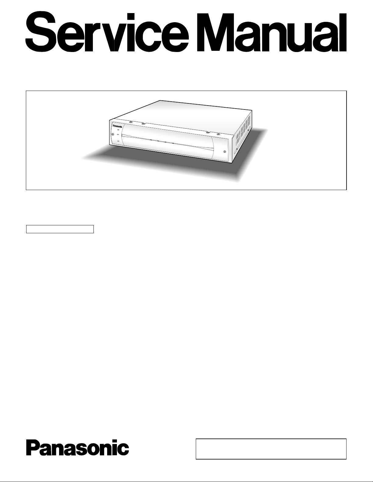
WJ-HDE300
WJ-HDE
300300
Extension Unit
SPECIFICATIONS
Matsushita Electric Industrial Co., Ltd.
All rights reserved. Unauthorized copying and
distribution is a violation of law.
©
2004
The Product with PbF
Required power: 120 V AC 60 Hz for WJ-HDE300
220 V AC - 240 V AC 50 Hz for WJ-HDE300/G
Power consumption: 85 W (including 4 HDDs when installed)
Interface: 2-wire serial, 480 Mbps logical speed
Operating temperature: +5 °C to +45 °C (41 °F to 113 °F)
Operating humidity: Less than 85 %
Dimensions: 420 mm (W) x 88 mm (H) x 350 mm (D), rubber feet exclusive
19-9/16" (W) x 3-7/16" (H) x 13-13/16" (D)
Weight: 7.2 k
g (16 lbs) (not including hard disk drives)
Weight and dimensions indicated are approximate.
Specifications are subject to change without notice.
CAUTION
RISK OF ELECTRIC SHOCK
DO NOT OPEN
CAUTION:
TO REDUCE THE RISK OF ELECTRIC SHOCK,
DO NOT REMOVE COVER (OR BACK). NO USER
SERVICEABLE PARTS INSIDE.
REFER SERVICING TO QUALIFIED SERVICE
PERSONNEL.
This symbol warns the user that uninsulated voltage within
the unit may have sufficient magnitude to cause electric
shock. Therefore, it is dangerous to make any kind of contact
with any inside part of this unit.
This symbol alerts the user that important literature concerning
the operation and maintenance of this has been included.
Therefore, it should be read carefully in order to avoid
any problems.
There are special components used in this equipment which are important for safety. These parts are indicated
by the ” Y ” mark on the schematic diagram and the replacement parts list. It is essential that these critical
parts should be replaced with manufacturer's specified parts to prevent X-radiation, shock, fire, or other hazards.
Do not modify the original design without permission of manufacture.
IMPORTANT SAFETY NOTICE
About Lead Free Solder (PbF)
Distribution of PbF PCB:
PCBs (manufactured) using lead free solder (PbF) will have a stamp on the PCB.
Caution:
8 Lead free solder has a higher melting point than standard solder. Typically the melting points is 35 °C – 40 °C
(95 °F – 104 °F) higher. Please use a soldering iron with temperature control and adjust it to 360 °C – 370 °C
(680 °F – 698 °F). In case of using high temperature soldering iron, please be careful not to heat too long.
8 Lead free solder will tend to splash when heated too high (600 °C / 1112 °F).
8 Lead free solder (Sn - 3.0Ag – 0.5Cu) or equivalents are recommended on repairing our lead free soldered PCB.
Y WARNING
This service information is designed for experienced repair technicians only and is not designed for use by the
general public.
It does not contain warnings or cautions to advise non-technical individuals of potential dangers in attempting to
service a product.
Products powered by electricity should be serviced or repaired only by experienced professional technicians. Any
attempt to service or repair the product or products dealt with in this service information by anyone else could
result in serious injury or death.
SAFETY PRECAUTIONS
GENERAL GUIDELINE
1. When service is required, observe the original lead
dress. Components, wires or cables that indicate
evidence of overheating or other electrical or mechanical
damage should be replaced.
2. After servicing see to that all the protective devices, such
as insulation tape, shields must be properly installed.
3. After servicing, make the following leakage current
checks to prevent the customer from being exposed to
shock hazards.
LEAKAGE CURRENT COLD CHECK
1. Unplug the AC cord and connect a jumper between the
two prongs on the plug.
2. Measure the resistance value, with an ohmmeter,
between the jumpered AC plug and each exposed
metallic cabinet part on the equipment such as
screwheads, connectors, control shafts, etc.
When the exposed metallic part has a return path to the
chassis, the reading should be between 1M Ω and 5.2M
Ω. When the exposed metal does not have a return path
to the chassis, the reading must be ∞ (infinity).
Any resistance value below this range indicates an
abnormality which requires corrective action.
3. Repeat the test with the AC switch in the "OFF" position.
LEAKAGE CURRENT HOT CHECK
1. Plug the AC cord directly into adaptor socket and plug
adaptor into the AC outlet. Do not use an isolation
transformer for this check.
2. Connect a 1.5k Ω/10W resistor, paralleled by 0.15 µF
capacitor, between each exposed metallic part on the
unit and a good earth ground such as a water pipe, as
shown in Figure 1.
3. Use an AC voltmeter, with 1000Ω/volt or more sensitivity,
to measure the potential across the resistor.
4. Check all exposed metallic parts of the cover (BNC
connector, Handle bracket, Metallic cabinet,
Screwheads, Metallic overlays, etc.), and measure the
voltage at each point.
5. Reverse the AC plug in the AC plug adaptor and re-peat
each of the above measurements.
6. The potential at any point should not exceed 0.75 V
RMS.
A leakage current tester (SIMPSON MODEL 229 or
equivalent) may be used to make the hot checks.
Leakage current must not exceed 0.5 milliampere.
In case a measurement is outside of the limits specified,
there is a possibility of a shock hazard, and corrective
action must be taken before returning the instrument to
the customer.
Fig. 1 Leakage Current Hot Check
PRODUCT COMPLIES WITH DHHS RULES 21 CFR SUBCHAPTER J APPLICABLE AT DATE OF MANUFACTURE
AC VOLTMETER
AC OUTLET
DEVICE
UNDER
TEST
ADAPTOR
AC PLUG
Ground Lead Disconnected during safety check.
Test all exposed
metal parts
1.5kΩ
0.15µF
Water Pipe
(Earth Ground)

CONTENTS
MAJOR OPERATING CONTROLS AND THEIR FUNCTIONS .........................................................1-1
WIRING DIAGRAM..............................................................................................................................2-1
SCHEMATIC DIAGRAM
MAIN BOARD (1/5)
PARTITION DIAGRAM..............................................................................................................3-1-1
[1]..............................................................................................................................................3-1-2
[2]..............................................................................................................................................3-1-3
[3]..............................................................................................................................................3-1-4
[4]..............................................................................................................................................3-1-5
MAIN BOARD (2/5)
PARTITION DIAGRAM..............................................................................................................3-2-1
[1]..............................................................................................................................................3-2-2
[2]..............................................................................................................................................3-2-3
[3]..............................................................................................................................................3-2-4
[4]..............................................................................................................................................3-2-5
MAIN BOARD (3/5) ..........................................................................................................................3-3
MAIN BOARD (4/5) ..........................................................................................................................3-4
MAIN BOARD (5/5) ..........................................................................................................................3-5
HDD-DC BOARD .............................................................................................................................3-6
POWER DIVIDER BOARD ..............................................................................................................3-7
FRONT SW BOARD ........................................................................................................................3-8
FRONT LED BOARD .......................................................................................................................3-9
AC/DC BOARD FOR WJ-HDE300.................................................................................................3-10
AC/DC BOARD FOR WJ-HDE300/G.............................................................................................3-11
CONDUCTOR VIEW
MAIN BOARD
(COMPONENT SIDE)...................................................................................................................4-1
(PATTERN SIDE)..........................................................................................................................4-2
HDD-DC BOARD .............................................................................................................................4-3
POWER DIVIDER BOARD / FRONT SW BOARD / FRONT LED BOARD .....................................4-4
AC/DC BOARD ................................................................................................................................4-5
EXPLODED VIEW
(1/6)..................................................................................................................................................5-1
(2/6)..................................................................................................................................................5-2
(3/6)..................................................................................................................................................5-3
(4/6)..................................................................................................................................................5-4
(5/6)..................................................................................................................................................5-5
(6/6)..................................................................................................................................................5-6
REPLACEMENT PARTS LIST............................................................................................................6-1
1-1
MAJOR OPERATING CONTROLS AND THEIR FUNCTIONS
■ Front View
ERROR
HDD 1 HDD 2 HDD 3 HDD 4
HDD
POWER
OPERATE
Extension Unit
WJ-HDE
qwe r t
q Error indicator [ERROR]
Lights when an error occurs. Refer to TROUBLESHOOTING for details.
Red: System error
Orange: Thermal error or malfunction of the cooling fan.
w HDD power indicator [HDD POWER]
ON: Indicates that HDDs are powered.
OFF: Indicates that the HDDs are not powered.
Note: Do not move the unit until the motors of the HDDs
stop completely. To stop the motors, turn off the
HDD POWER switch behind the front cover. Move
the unit after confirming that the indicator has gone
out.
e Operate indicator [OPERATE]
Lights green when turning on the power switch on the
rear panel.
r HDD access indicators [HDD 1] [HDD 2] [HDD 3]
[HDD 4]
Each indicator lights to indicate the status of the respective HDD.
Green: Indicates that the respective HDD is running
normally.
Red: Indicates that the respective HDD is the first faulty
drive among the HDDs in the unit.
Red blink: Indicates that the respective HDD is the sec-
ond or subsequent faulty drive among the HDDs in
the unit.
Orange-red alternate blink/Orange: Indicates that the
respective drive is currently being recovered in
RAID level 5 mode.
These indicators normally indicate the status of the
respective drive, but they work as a set when a system
error occurs.
Important
When one of the indicators lights red, replace the
respective HDD immediately. If two or more indicators
light/blink red, it will be impossible to recover data.
There may be cases where it is eventually impossible to
recover data if two drives are coincidentally damaged or
the second drive fails during the data recovery process.
t Front cover
Detach the front cover when it is necessary to install
HDDs or to operate the switches inside the unit.
1-2
y Serial in connector [IN]
Connect the WJ-HD300 series digital disk recorder or
other extension unit with the supplied serial cable.
u Serial out connector [OUT1] [OUT2]
Connect another extension unit with the supplied serial
cable.
i Cooling fan
o Signal GND terminal [SIGNAL GND]
Connect this terminal to the SIGNAL GND terminal of
other equipment to avoid possible grounding loop and
noise if required.
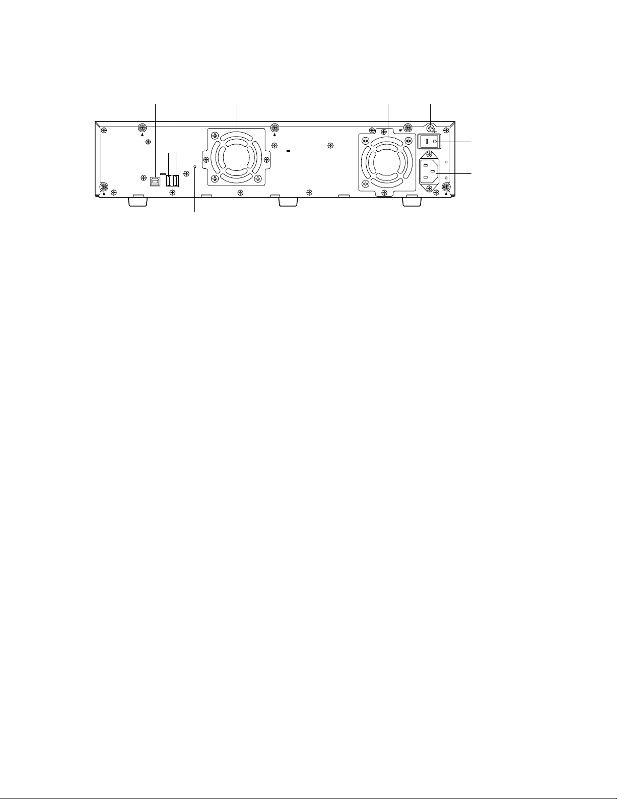
!0 Power switch [POWER]
Turn on the power of the unit with this switch before turning on the power of the digital disk recorder, or turn
them on simultaneously. Otherwise, the HDDs will not be
mounted.
When turning off the power of the unit with this switch,
turn off the power of the digital disk recorder first, and
then turn off the power of this unit after confirming that
all HDD access indicators are not lit or blinking.
!1 AC inlet [AC IN]
Connect the supplied power cord.
!2 Cable clamp fixing hole
■ Rear View
POWER
AC IN
SIGNAL GND
12
IN OUT
EXT
yu i i
o
!0
!1
!2

1-3
q' Error indicators
Functions as same as that on the front panel.
Red: System error
Orange: Thermal error or malfunction of the cooling fan.
w'HDD power indicator
Functions as same as that on the front panel.
ON: Indicates that HDDs are powered.
OFF: Indicates that the HDDs are not powered.
e'Operate indicator
Functions as same as that on the front panel.
Lights green when turning on the power switch on the
rear panel.
!3 Reset button [RESET]
This button is located inside the unit. To access this button, it is necessary to detach the front cover. Press this
button using a small screw driver (not supplied).
• When SINGLE is selected
After adding or replacing any of the HDDs, press this
button only.
• When RAID 5 is selected
This button is used in combination with the RECOVER
button and MODE switch after adding or replacing any
of the HDDs.
Important
Do not press the RESET button and the RECOVER
button simultaneously when SINGLE is selected.
Otherwise, the setting of the digital disk recorder
may be initialized and it may cause a malfunction.
!4 Mode switch [MODE]
RAID 5: Applies RAID level 5 mode (striping at the byte
level also stripe error correction information).
SINGLE: Applies SINGLE mode (no striping across dri-
ves for data or error correction information). Default
position
■ Inside the Front Lid
!3
!4
!5
!6
SINGLE RAID5
MODE
RESET
HDD POWER
RECOVER
OFF ON
w’
e’
q’
Important
• Changing the MODE switch will not be accepted when
the ERROR indicator lights red and/or when HDD 1-4
indicate a system error status by lighting red and
orange. When this happens, ask your dealer to solve
the error.
• When set to RAID5, the HDD preinstalled in the digital
disk recorder will not work. Instead, it is applied only to
the HDDs installed in the extension unit and the digital
disk recorder will perform storage and readout of the
image data by accessing the extension unit.
• The position of the MODE switch of all units in a system
must be the same.
• The available disk space of the unit can be logically calculated as follows. The actual space may be several
percent lower than you calculated depending on the
HDD type used and their combination. The most efficient way is to use the same type drives.
When SINGLE is selected, it will be the sum of all
the HDD sizes.
When RAID 5 is selected, it will be as follows.
When 3 HDDs are in the unit: It will be double the
size of the smallest HDD size.
When 4 HDDs are in the unit: It will be triple the size
of the smallest HDD size.
For example, if 4 HDDs of 80 GB, 120 GB, and two
160 GB are mounted, the available disk space will
be 80 G x 3 = 240 GB.
!5 HDD power switch [HDD POWER]
Use this switch in the ON position for normal operation.
ON: Supplies the power to the HDDs and the HDD
power indicators will light. Default position
OFF: Does not supply the power and the HDD power
indicators will go off.
!6 Recover button [RECOVER]
Use this button with the RESET button after replacing
HDDs used in the RAID 5 mode to start data recovery.
2-1
WIRING DIAGRAM
MO3
COOLING
FAN-3
SW11
POWER SWITCH
L11
FERRITE CLAMP
CN11
AC INLET
MO4
COOLING
FAN-4
MO2
COOLING
FAN-2
MO1
COOLING
FAN-1
TO HDD
HDD 2
TO HDD
HDD 1
TO HDD
HDD 4
TO HDD
HDD 3
113
3
3
1
5
7
57
13
CN1
CN2
E13
E14
E15
E26
E11
E20 E23
E21
E17
E16
E19
E18
E22
E24
E25
E12
19
210
CN3
13
CN520
119
110
10 1
220
CN100
119
220
9
10
1
2
CN550
CN500
31
CN522
10 1
10
1
1
2
1
2
39
40
39
40
414 14
1
CN101
CN100
CN102
CN201
CN202
1
2
1
2
39
40
39
31
40
CN203
CN521
CN200
CN103 CN104
14
CN105
111
122
101
CN100
CN102
101
13
CN101
CN523
CN101
CN100
MAIN BOARD
AC/DC
BOARD
HDD-DC
BOARD
POWER
DIVIDER
BOARD
FRONT LED BOARDFRONT SW BOARD
3-1-1
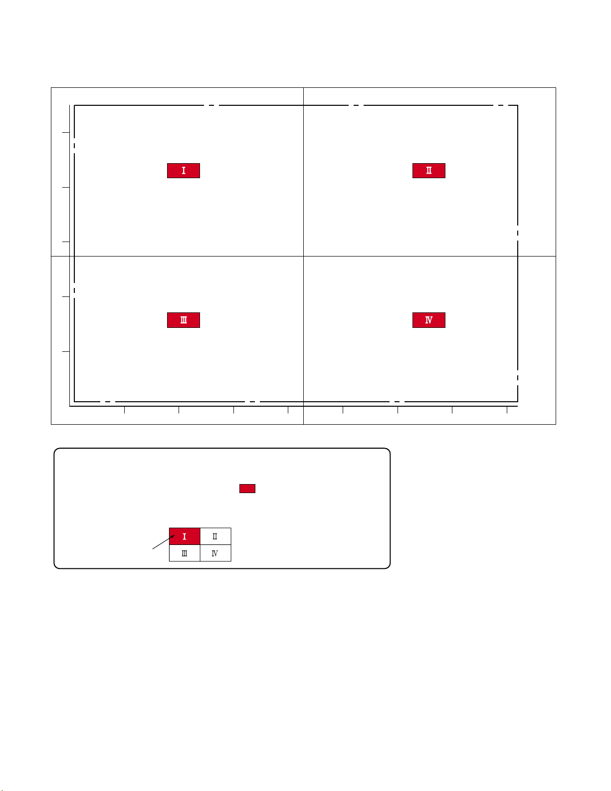
PARTITION DIAGRAM FOR SCHEMATIC DIAGRAM
OF MAIN BOARD (1/5)
<LOCATION MARK>
(Refer to the page 3-1-2.)
(Refer to the page 3-1-4.)
(Refer to the page 3-1-3.)
(Refer to the page 3-1-5.)
• The Location Mark indicated in each Schematic Diagram of Main Board (1/5) is as follows.
<Example>
For Schematic Diagram
of Main Board (1/5) [1] :
• The Schematic Diagram of Main Board (1/5) is described by 4 partitions.
• When connecting all the Schematic diagram, refer to this Partition Diagram.
Location of each Schemaitc diagram is marked ( ) in the diagram.
Location Mark
MAIN BOARD (1/5)
1
A
B
C
D
E
F
2345678
3-1-2
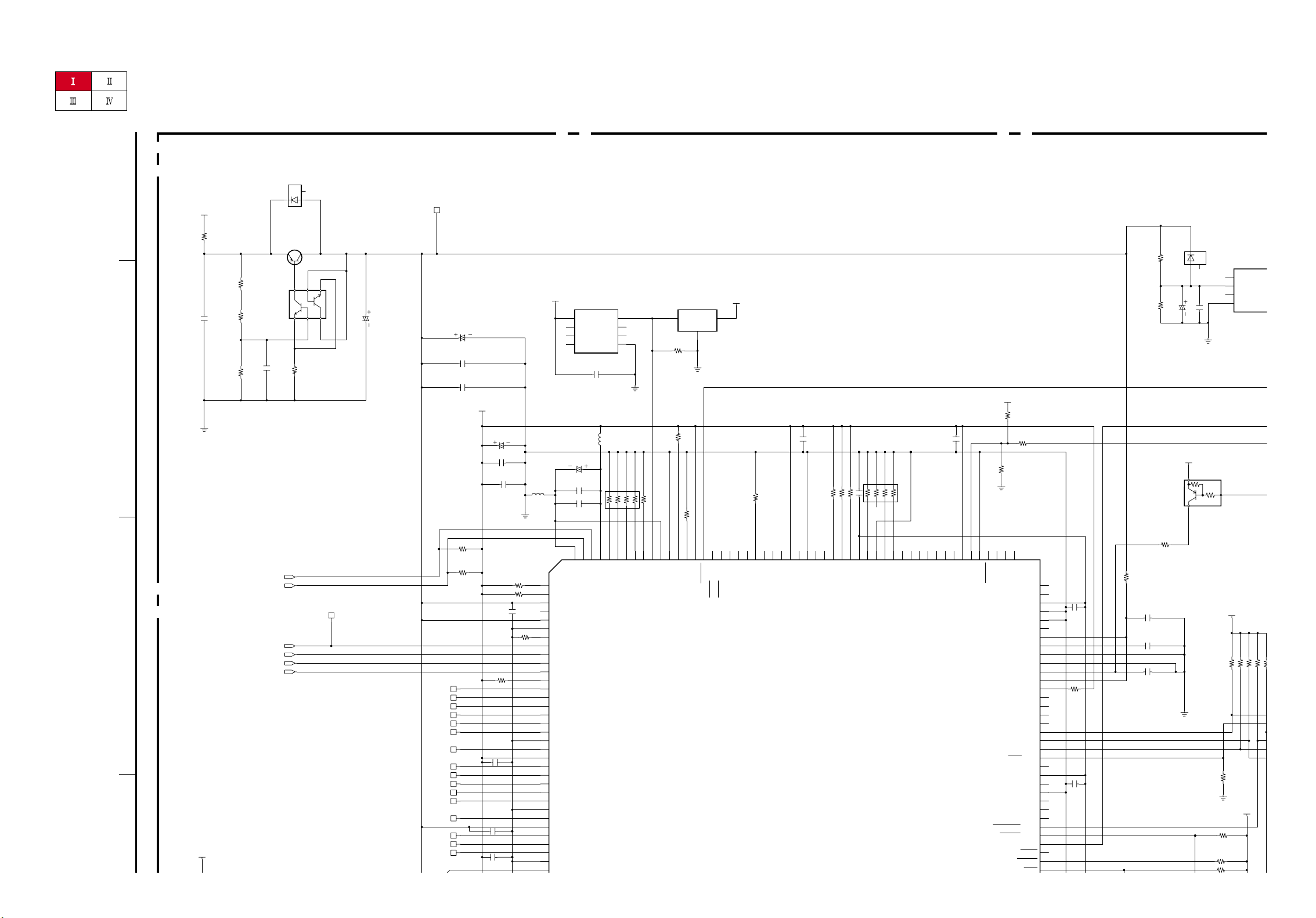
SCHEMATIC DIAGRAM OF MAIN BOARD (1/5) [1]
<LOCATION MARK>
D[15]
R111 10k
R133 10k
TD116
Q100
D101
TD104
R103
470
C156 0.1
TD107
R104
330
1/4W
XINIT
Q101
1
25
34
6
R110
10k
V5D
TD100
C133
0.1
XDONE
R101
330
IC
1
NC_1
2
INPUT
3
NC_2
4
GND
SU
TD115
TD113
IRQ1
V3D
IC102
OPEN
1
+VS
2
VOUT
3
GND
R102
15
TD117
R112 10k
IRQ3
V3D
Q102
C113
0.1
V3D
R108
10k
C117
47/6.3
V5D
C120
0.1
R163
OPEN
OPEN
C100
1
DGND
C135 0.1
C131
0.1
C121
0.1
DGND
R113
10k
R109
10k
R116
10k
10k
10k
R125
OPEN
TD103
TD110
C110
0.01
V3D
IRQ0
R118
10k
IRQ2
V3D
TD105
Z110
123
45
678
DGND
C137 470p
R123 10k
C108
OPEN
R119 10k
C126
0.1
DGND
R161
0
R138
10k
C119
0.01
V3D
R137
10k
TD106
TD111
R164
51k
C136 470p
IC101
1
MD1
2
MD2
3
Vcc_1
4
NC
5
Vcc_2
6
Vss_1
7
NMI
8
IRQ0/PTH[0]
9
IRQ1/PTH[1]
10
IRQ2/PTH[2]
11
IRQ3/PTH[3]
12
IRQ4/PTH[4]
13
D31/PTB[7]
14
D30/PTB[6]
15
D29/PTB[5]
16
D28/PTB[4]
17
D27/PTB[3]
18
D26/PTB[2]
19
VssQ_1
20
D25/PTB[1]
21
VccQ_1
22
D24/PTB[0]
23
D23/PTA[7]
24
D22/PTA[6]
25
D21/PTA[5]
26
D20/PTA[4]
27
Vss_2
28
D19/PTA[3]
29
Vcc_3
30
D18/PTA[2]
31
D17/PTA[1]
32
D16/PTA[0]
33
VssQ_2
34
D15
123
124
RESETM
125
PTH[5]/ADTRG
126
PTG[7]
127
ASEMD0/PTG[6]
128
ASEBRKAK/PTG[5]
129
UCLK/PTG[4]
130
AUDATA[3]/PTG[3]
131
AUDATA[2]/PTG[2]
132
Vss_4
133
AUDATA[1]/PTG[1]
134
Vcc_5
135
AUDATA[0]/PTG[0]
136
TRST/PTF[7]
137
TMS/PTF[6]
138
TDI/PTF[5]
139
TCK/PTF[4]
140
DMNS/PTF[3]
141
DPLS/PTF[2]
142
TXDPLS/PTF[1]
143
TXDMNS/PTF[0]
144
MD0
145
Vcc-PLL1
146
CAP1
147
Vss-PLL1
148
Vss-PLL2
149
CAP2
150
Vcc-PLL2
151
AUDCK/PTH[6]
152
Vss_5
153
Vss_6
154
Vcc_6
155
XTAL
156
EXTAL
157
STATUS0/PTJ[6]
158
STATUS1/PTJ[7]
159
TCLK/PTH[7]
160
IRQOUT
161
VssQ_9
162
CKIO
163
VccQ_9
164
TXD0/SCPT[0]
165
SCK0/SCPT[1]
166
TXD1/SCPT[2]
167
SCK1/SCPT[3]
168
TXD2/SCPT[4]
169
SCK2/SCPT[5]
170
SCPT[6]
171
RXD0/SCPT[0]
172
RXD1/SCPT[2]
173
Vss_7
174
RXD2/SCPT[4]
175
Vcc_7
176
IRQ5/SCPT[7]
177
IRQ6/PTC[7]
178
IRQ7/PTC[6]
179
XVDATA/PTC[5]
180
TXENL/PTC[4]
181
VssQ_10
182
VBUS/PTD[3]
183
VccQ_10
184
SUSPND/PTD[2]
185
NF/PTC[3]
186
NF/PTC[2]
187
NF/PTC[1]
188
PTC[0]
189
DRAK0/PTD[1]
190
DRAK1/PTD[0]
191
DREQ0/PTD[4]
192
DREQ1/PTD[6]
193
RESETP
194
VccQ_11
195
MD3
196
MD4
197
Vss_8
198
Avss_1
199
AN[0]/PTL[0]
200
AN[1]/PTL[1]
201
AN[2]/PTL[2]
202
AN[3]/PTL[3]
203
PTL[4]
204
PTL[5]
205
AVcc
206
PTL[6]
207
PTL[7]
208
Avss_2
C118
0.1
TD112
C114
0.1
C152
0.1
Z111
123
45
678
R132
10k
C105
47/6.3
C129 0.1
L101
R162
100
C109
0.1
R117
10k
C132
0.1
C122
0.01
D100
C155
33/6.3
R136
10k
R124
OPEN
R131 10k
R121 10k
L100
R122 10k
DGND
DGND
DGND
C115
0.1
DGND
R140
10k
R139
10k
C102
0.47
TD114
TD108
TD102
TD101
R127
10k
R120
10k
C123
100/6.3
R100
0
TD109
R126
0
R134 470
V3D
IC108
1
VOUT
2
N.C._1
3
N.C._2
4
GND
5
N.C._3
6
N.C._4
7
N.C._5
8
+VS
+1.9V
MAIN BOARD (1/5)
D
E
F
3-1-3
SCHEMATIC DIAGRAM OF MAIN BOARD (1/5) [2]
<LOCATION MARK>
A[16]
A[9]
A[10]
A[11]
A[12]
A[13]
A[14]
A[15]
A[18]
A[8]
A[7]
A[6]
A[5]
A[4]
A[3]
A[2]
D[15]
D[7]
D[14]
D[6]
D[13]
D[5]
D[12]
D[4]
D[11]
D[3]
D[2]
D[9]
D[1]
D[8]
A[1]
D[10]
D[0]
A[17]
D[1]
D[2]
D[3]
D[0]
D[7]
D[6]
D[5]
D[4]
A[13]
A[14]
A[11]
A[1]
A[2]
A[3]
A[4]
A[12]
A[10]
A[9]
A[8]
A[7]
A[6]
A[5]
D[8]
D[12]
D[13]
D[14]
D[15]
D[11]
D[10]
D[9]
R141
10k
C147
0.1
IC107
1
NC
2
IN_A
3
GND
4
OUT_Y
5
VCC
A[1-25]
C156 0.1
V3D
C145
0.1
C157 0.1
C149
0.1
R155
OPEN
IC111
1
NC_1
2
INPUT
3
NC_2
4
GND
5
NC_3
6
OUTPUT
7
SUPPLY_VOLTAGE
8
NC_4
Z119
1
2
3
45
6
7
8
DGND
Z112
22 22
22
22
22
22
22
1
2
3
45
6
7
8
R143
OPEN
R152
47
R142
22
R149
0
V3D
V3D
OPEN
Z118
1
2
3
45
6
7
8
V3D
R146
33
C141
0.1
R151
OPEN
DGND
V3D
DGND
C143
33/6.3
IC103
1
A15
2
A14
3
A13
4
A12
5
A11
6
A10
7
A9
8
A8
9
N.C._1
10
N.C._2
11
WE
12
RESET
13
N.C._3
14
N.C._4
15
RY/BY
16
N.C._5
17
A17
18
A7
19
A6
20
A5
21
A4
22
A3
23
A2
24
A1
25
A0
26
CE
27
VSS_1
28
OE
29
DQ0
30
DQ8
31
DQ1
32
DQ9
33
DQ2
34
DQ10
35
DQ3
36
DQ11
37
VCC
38
DQ4
39
DQ12
40
DQ5
41
DQ13
42
DQ6
43
DQ14
44
DQ7
45
DQ15/A-1
46
VSS_2
47
BYTE
48
A16
C144
0.1
Z113
1
2
3
45
6
7
8
TD120
C158 0.1
R138
10k
R137
10k
DGND
DGND
C138
0.1
X100
(66.666MHz)
1
CONT
2
GND
3
OUT
4
VDD
V3D
C142
0.1
C151
0.1
R144
OPEN
R132
10k
Z114
22
Z115
22
Z116
1
2
3
45
6
7
8
CN100
OPEN
1
3
5
7
910
8
6
4
2
11 12
13 14
V3D
C140
0.1
R136
10k
DGND
R131 10k
Z117
1
2
3
45
6
7
8
IC104
1
VDD_1
2
DQ0
3
VDDQ_1
4
DQ1
5
DQ2
6
VSSQ_1
7
DQ3
8
DQ4
9
VDDQ_2
10
DQ5
11
DQ6
12
VSSQ_2
13
DQ7
14
VDD_2
15
LDQM
16
WE
17
CAS
18
RAS
19
CS
20
BA0
21
BA1
22
A10/AP
23
A0
24
A1
25
A2
26
A3
27
VDD_328VSS_1
29
A4
30
A5
31
A6
32
A7
33
A8
34
A9
35
A11
36
NC_1
37
CKE
38
CLK
39
UDQM
40
NC_2
41
VSS_2
42
DQ8
43
VDDQ_3
44
DQ9
45
DQ10
46
VSSQ_3
47
DQ11
48
DQ12
49
VDDQ_4
50
DQ13
51
DQ14
52
VSSQ_4
53
DQ15
54
VSS_3
C139
0.1
DGND
DGND
R140
10k
C146
33/6.3
R139
10k
1
2
3
45
6
7
8
Z120
1
2
3
45
6
7
8
V3D
V3D
1
2
3
45
6
7
8
D[0-15]
66.666MHz
<INDEX>
IC100 A2
IC101 B2,B3,B4,
C2,C3,C4,
D2,D3,D4
IC103 E6,F6
IC104 C6,D6
IC105 B7,C7
IC106 B8,C8
IC107 C8,D8
IC108 E2
IC109 A3,A4
IC110 A4
IC111 E5,F5
Q100 E1,F1
Q101 E1
Q102 E5
D100 F1
MAIN BOARD (1/5)

3-1-4
SCHEMATIC DIAGRAM OF MAIN BOARD (1/5) [3]
<LOCATION MARK>
A[1]
A[2]
A[3]
A[4]
A[5]
A[6]
A[7]
A[8]
A[9]
A[10]
A[11]
A[12]
A[13]
A[14]
A[15]
A[16]
A[17]
A[19]
A[20]
A[21]
A[22]
A[23]
A[24]
D[0]
D[1]
D[2]
D[3]
D[4]
D[5]
D[6]
D[7]
D[8]
D[9]
D[10]
D[11]
D[12]
D[13]
D[14]
D[15]
A[25]
A[1]
A[2]
A[3]
A[4]
A[5]
A[6]
A[7]
A[8]
A[9]
A[10]
A[11]
A[12]
A[13]
A[14]
A[15]
A[16]
A[17]
A[18]
A[19]
A[20]
A[21]
A[22]
A[23]
A[24]
A[25]
A[18]
D[15]
D[14]
D[13]
D[12]
D[11]
D[10]
D[9]
D[8]
D[7]
D[6]
D[5]
D[4]
D[3]
D[2]
D[1]
D[0]
XCSZ
Z106
1
2
3
45
6
7
8
R133 10k
TD116
C130
0.1
Z107
1
2
3
45
6
7
8
R115
33
Z100
OPEN
1
2
36
45
45
45
45
7
8
IC110
1
IN_B
2
IN_A
3
GND4OUT_Y
5
VCC
C111
0.1
TD115
C124
0.1
CSRZ
DGND
TD117
R106
10k
0.1
DGND
DGND
R158
10
C154 0.1
C116
0.1
V12D
SW101
OPEN
24
13
Z108
1
2
3
45
6
7
8
Z109
1
2
3
45
6
7
8
V5D
IC109
1
NC_1
2
INPUT
3
NC_2
4
GND
5
NC_3
6
OUTPUT
7
SUPPLY_VOLTAGE
8
NC_4
DGND
C112
10/16
R130
OPEN
R129
OPEN
R128
470
XWRTZ
C127
0.1
R160
1k
C134
0.1
R165
OPEN
V3D
Z102
1
2
36
7
8
SW100
OPEN
1
2
3
4
5
V3D
C103
0.1
C128
0.1
R107
10k
R166
OPEN
C101
0.1
V3D
C104
0.1
Vcc_3
30
D18/PTA[2]
31
D17/PTA[1]
32
D16/PTA[0]
33
VssQ_2
34
D15
35
VccQ_2
36
D14
37
D13
38
D12
39
D11
40
D10
41
D9
42
D8
43
D7
44
D6
45
VssQ_3
46
D5
47
VccQ_3
48
D4
49
D3
50
D2
51
D1
52
D0
53A054A155A256A357
VssQ_458A459VccQ_460A561A662A763A864A965A1066A1167A1268A1369VssQ_570A1471VccQ_572A1573A1674A1775A1876A1977A2078A2179Vss_380A2281Vcc_482A2383VssQ_684A2485VccQ_686A2587BS/PTK[4]88RD89WE0/DQMLL
90
WE1/DQMLU
91
WE2/DQMUL/PTK[6]
92
WE3/DQMUU/PTK[7]
93
RD/WR94AUDSYNC/PTE[7]
95
VssQ_796CS097VccQ_798CS2/PTK[0]
99
CS3/PTK[1]
100
CS4/PTK[2]
101
CS5/PTK[3]
102
CS6
103
PTE[4]
104
PTE[5]
105
CKE/PTK[5]
106
RAS3L/PTJ[0]
107
NF/PTJ[1]
108
CASL/PTJ[2]
109
VssQ_8
110
CASU/PTJ[3]
111
VccQ_8
112
NF/PTJ[4]
113
NF/PTJ[5]
114
DACK0/PTD[5]
115
DACK1/PTD[7]
116
PTE[6]
117
PTE[3]
118
RAS3U/PTE[2]
119
PTE[1]
120
TDO/PTE[0]
121
BACK
122
BREQ
123
WAIT
124
RESETM
125
PTH[5]/ADTRG
126
PTG[7]
127
ASEMD0/PTG[6]
ASEBRKAK/PTG[5]
C114
0.1
Z105
1
2
3
45
6
7
8
RSTI
R105
100
R114
470
XPRGZ
V3D
R135 10k
R131 10k
IC100
1
VREF
2
RESIN
3
CT
4
GND5RESET
6
RESET
7
VSSENSE
8
VCC
V3D
Z103
OPEN
OPEN
OPEN
1
2
36
7
8
C125
0.1
R157
1k
R159
OPEN
C107
0.1
TD118
C153
0.1
R156
1k
Z104
1
2
3
45
6
710k
10k
10k
10k
10k
10k
8
Z101
1
2
36
7
8
TD119
R134 470
DGND
C106
2.2/50
1
A
B
C
234
3-1-5
SCHEMATIC DIAGRAM OF MAIN BOARD (1/5) [4]
<LOCATION MARK>
R133 10k
TD125
R145
56
TP100
OPEN
WAITZ
CPUCLK
PORSTN
DGND
IC106
1
1A
2
1B
3
1Y
4
2A
5
2B
6
2Y
7
GND83Y
9
3A
10
3B
11
4Y
12
4A
13
4B
14
VCC
XCLK
DGND
CSZ
V3D
SW101
OPEN
24
13
R148
22
R130
OPEN
DGND
TD124
BSZ
R154
68
WRZ
R150
68
TD121
TD122
C148
0.1
TD123
R153
68
DGND
RDZ
WE1Z
IC105
1
1CLR
2
1D
3
1CLK
4
1PRE
5
1Q
6
1Q
7
GND82Q
9
2Q
10
2PRE
11
2CLK
12
2D
13
2CLR
14
VCC
V3D
R135 10k
TD126
DCLK
R131 10k
DGND
C150
0.1
R147
10k
R134 470
WE0Z
33.333MHz
33.333MHz
5678

3-2-1
PARTITION DIAGRAM FOR SCHEMATIC DIAGRAM
OF MAIN BOARD (2/5)
<LOCATION MARK>
(Refer to the page 3-2-2.)
(Refer to the page 3-2-4.)
(Refer to the page 3-2-3.)
(Refer to the page 3-2-5.)
• The Location Mark indicated in each Schematic Diagram of Main Board (2/5) is as follows.
<Example>
For Schematic Diagram
of Main Board (2/5) [1] :
• The Schematic Diagram of Main Board (2/5) is described by 4 partitions.
• When connecting all the Schematic diagram, refer to this Partition Diagram.
Location of each Schemaitc diagram is marked ( ) in the diagram.
Location Mark
9
A
B
C
D
E
F
G
H
MAIN BOARD (2/5)
10 11 12 13 14 15 16 17 18 19
 Loading...