Panasonic uf-4500 service manual
ORDER NO.KMF1103351CE
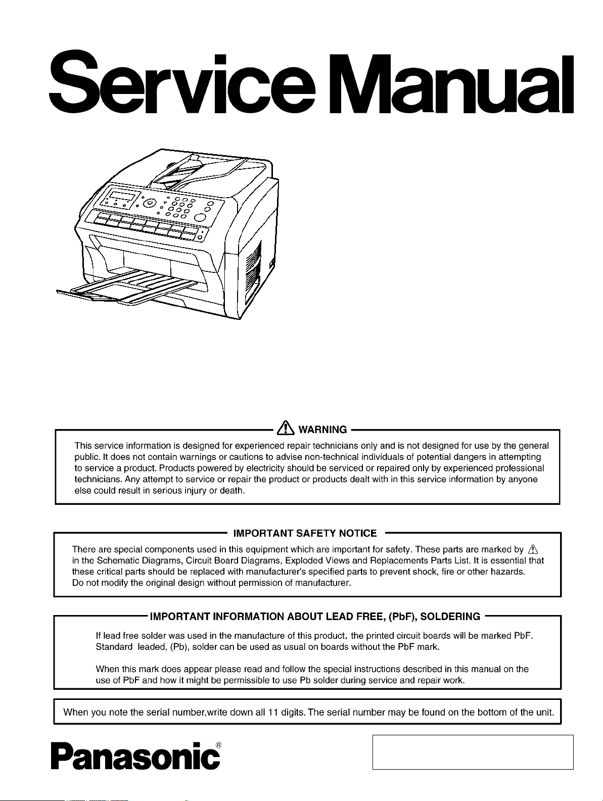
Facsimile Transceiver
Model No. UF-5500
UF-4500
(for U.S.A and CANADA)
F7
© Panasonic System Networks Co., Ltd. 2011
Unauthorized copying and distribution is a violation
of law.

UF-5500 / 4500
TABLE OF CONTENTS
1 Safety Precautions -----------------------------------------------5
1.1. For Service Technicians----------------------------------5
1.2. AC Caution---------------------------------------------------5
1.3. Personal Safety Precautions ----------------------------6
1.3.1. Moving Sections of the Unit-------------------------6
1.3.2. Live Electrical Sections ------------------------------6
1.4. Service Precautions ---------------------------------------6
1.4.1. Precautions to Prevent Damage from
Static Electricity ----------------------------------------6
2Warning--------------------------------------------------------------7
2.1. About Lead Free Solder (PbF: Pb free) --------------7
2.1.1. Suggested PbF Solder -------------------------------7
2.2. Disposing of the P. C. Board ----------------------------8
2.3. Insulation Resistance Test -------------------------------8
2.4. Battery Caution ---------------------------------------------8
2.5. Laser Beam and Fuser Unit Section ------------------9
2.6. Note for Repairing------------------------------------------9
3 Specifications ---------------------------------------------------- 10
3.1. Fax Function----------------------------------------------- 10
3.2. Printer & Scanner Function (UF-5500 only) ------- 19
4 General/Introduction------------------------------------------- 20
4.1. Optional Accessories------------------------------------ 20
5 Hardware Requirements for Printer Driver and
Application Software------------------------------------------- 21
6 Technical Descriptions---------------------------------------- 22
6.1. Connection Diagram------------------------------------- 22
6.2. General Block Diagram --------------------------------- 23
6.3. Main Board Section-------------------------------------- 25
6.3.1. Data Flow---------------------------------------------- 25
6.3.2. RTC Backup Circuit --------------------------------- 34
6.3.3. Modem Circuit Operation -------------------------- 34
6.3.4. TEL Line Section ------------------------------------ 35
6.4. NCU Section----------------------------------------------- 36
6.4.1. General ------------------------------------------------ 36
6.4.2. EXT. TEL. Line Relay (RLY100) ----------------- 36
6.4.3. Bell Detection Circuit ------------------------------- 36
6.4.4. Remote FAX Activation Circuit ------------------- 36
6.4.5. TAM Interface Circuit ------------------------------- 36
6.5. ITS (Integrated Telephone System) and
Monitor Section -------------------------------------------37
6.5.1. General ------------------------------------------------ 37
6.6. CIS Control Section-------------------------------------- 38
6.7. Motor Drive Section-------------------------------------- 39
6.7.1. Engine Motor Control Circuit --------------------- 39
6.7.2. Scanner Motor Drive Circuit ---------------------- 41
6.8. Timing Chart and Waveform of Scanner
Motors------------------------------------------------------- 44
6.8.1. Normal 1-2 phase excitation (half step)-------- 44
6.8.2. Flat torque 1-2 phase excitation (half step) --- 45
6.8.3. W1-2 phase excitation (Quarter step) ---------- 46
6.8.4. Drive mode of ADF motor -------------------------47
6.9. FAN Motor Section--------------------------------------- 47
6.9.1. General ------------------------------------------------ 47
6.9.2. Circuit Diagram of FAN ---------------------------- 48
6.9.3. Fan Control ------------------------------------------- 48
6.9.4. Control table ------------------------------------------49
6.9.5. Waveform---------------------------------------------- 49
6.10. Solenoid Driver Section -------------------------------- 50
6.11. LSU (Laser Scanning Unit) Section ----------------- 51
PAG E PAG E
6.12. Sensors and Switches Section ----------------------- 53
6.12.1. Drum Detection ------------------------------------- 54
6.12.2. Pickup Sensor --------------------------------------- 54
6.12.3. Exit Sensor ------------------------------------------- 55
6.12.4. Read Position Sensor------------------------------ 55
6.12.5. Registration Sensor -------------------------------- 56
6.12.6. Print Timing Sensor -------------------------------- 56
6.12.7. Document Sensor----------------------------------- 57
6.12.8. Top Cover Sensor----------------------------------- 57
6.12.9. Toner Sensor.... “Out of Toner”, “Toner
Low”, “Replace Drum” ----------------------------- 58
6.12.10. ADF Cover Open Switch -------------------------- 61
6.13. Operation Board Section ------------------------------ 62
6.14. LCD Section----------------------------------------------- 63
6.15. HVPS (High Voltage Power Supply) Section ----- 64
6.15.1. HVPS Specification--------------------------------- 64
6.15.2. CHG-BIAS (Charge BIAS)/GRID/ UNIT ------- 64
6.15.3. DEV DC BIAS UNIT -------------------------------- 65
6.15.4. DEV AC BIAS UNIT -------------------------------- 65
6.15.5. TRA (+) BIAS (Transfer (+) BIAS)/TRA (-)
BIAS (Transfer (-) BIAS) UNIT------------------- 65
6.16. Heat Lamp Control Circuit ----------------------------- 66
6.17. Main Board Section ------------------------------------- 69
6.18. Power Supply Board Section ------------------------- 72
6.19. Mechanical Operation ---------------------------------- 73
6.19.1. Printing ------------------------------------------------ 73
6.19.2. Scanning (ADF) ------------------------------------ 73
7 Location of Controls and Components ----------------- 74
7.1. Overview --------------------------------------------------- 74
7.2. Control Panel --------------------------------------------- 75
7.2.1. Control Panel - For only U.S.A. (AU) -------- 75
7.2.2. Control Panel - For only CANADA (AC) ---- 76
8 Installation Instructions -------------------------------------- 77
8.1. Installation ------------------------------------------------- 77
8.1.1. Installation Space ----------------------------------- 77
8.1.2. DOCUMENT TRSAY AND RECORDING
PAPER TRAY ---------------------------------------- 78
8.1.3. RECORDING PAPER----------------------------- 79
8.1.4. Documents the Unit Can Send ------------------ 81
8.1.5. Toner Cartridge and the Drum Cartridge------ 83
8.1.6. When Connecting using a USB Port (UF5500 only)--------------------------------------------- 86
8.1.7. When Connecting using a Network Port
(UF-5500 only)--------------------------------------- 87
8.2. Connections----------------------------------------------- 88
9 User Mode--------------------------------------------------------- 89
9.1. Fax Parameter Table ----------------------------------- 89
10 Service Mode----------------------------------------------------- 92
10.1. Service Modes (For Facsimile)----------------------- 92
10.1.1. Service Mode Table -------------------------------- 92
10.1.2. Service Mode 1 (Function Parameter
Setting) ------------------------------------------------ 93
10.1.3. Service Mode 3 (Printout of Lists, Reports
and Test Results) ----------------------------------- 99
10.1.4. Service Mode 4 (Modem Test)------------------ 110
10.1.5. Service Mode 5 (Diagnostic) -------------------- 114
10.1.6. Service Mode 6 (RAM Initialization) ----------- 115
10.1.7. Service Mode 7 (LBP Service Mode) --------- 116
10.1.8. Service Mode 8 (Check & Call)----------------- 117
2

UF-5500 / 4500
10.1.9. Service Mode 9 (System Maintenance) ------122
11 Troubleshooting Guide-------------------------------------- 124
11.1. Starting Troubleshooting------------------------------ 124
11.1.1. Outline ------------------------------------------------124
11.1.2. Improper LCD Display ----------------------------125
11.2. Troubleshooting Details------------------------------- 126
11.2.1. Initialization ------------------------------------------ 126
11.2.2. Simplified Troubleshooting Guide ------------- 127
11.2.3. Safety Error Information Troubleshooting
Guide ------------------------------------------------- 130
11.2.4. Print --------------------------------------------------- 136
11.2.5. Recording Paper Feed --------------------------- 143
11.2.6. ADF (Auto Document Feeder) Section ------- 148
11.2.7. Communications -----------------------------------154
11.2.8. Information Codes Table (For Facsimile) ---- 157
11.2.9. Diagnostic Codes (For Facsimile) ------------- 161
11.2.10. Analog Section ------------------------------------- 168
11.2.11. Operation Panel Section ------------------------- 171
11.2.12. Sensor Section -------------------------------------171
11.2.13. Motor Section ---------------------------------------174
11.2.14. LSU Section ----------------------------------------- 176
11.2.15. CIS Control Section -------------------------------177
11.2.16. High Voltage Value Check Point --------------- 179
11.2.17. High Voltage Section------------------------------ 181
11.2.18. USB Section (UF-5500 only)-------------------- 186
11.2.19. LAN SECTION (UF-5500 only)----------------- 190
11.2.20. Main Board Section ------------------------------- 195
11.2.21. Power Supply Board Section ------------------- 198
11.3. Information Codes (INFO. CODES) --------------- 200
11.3.1. Information Codes: 400, 420-------------------- 202
11.3.2. Information Codes: 401, 402, 422 ------------- 203
11.3.3. Information Codes: 404, 405, 407 ------------- 204
11.3.4. Information Code: 416 ---------------------------- 205
11.3.5. Information Codes: 408, 409, 417, 418,
490 ---------------------------------------------------- 206
11.3.6. Information Code: 434 ---------------------------- 207
11.3.7. Information Codes: 459, 494, 495 ------------- 208
11.3.8. Information Codes: 001, 007 (Recording
Paper Jam) ------------------------------------------ 209
11.3.9. Information Codes: 030, 031 (Document
Jam)--------------------------------------------------- 210
11.3.10. Information Code: 630 (Dialing Error) -------- 210
11.3.11. Information Codes: 403, 411, 414, 415
(Polling Operator Trouble)----------------------- 211
11.4. Clearing a Document Jam---------------------------- 212
11.5. Clearing a Recording Paper Jam------------------- 213
11.5.1. When the recording paper is not fed into
the unit properly ------------------------------------ 214
11.6. Cleaning the Document Scanning Area ---------- 214
12 Disassembly and Assembly Instructions ------------- 215
12.1. ADF Section --------------------------------------------- 216
12.2. Remove ADF Section(1)------------------------------ 217
12.3. Remove Pickup-Roller-Cover Unit ----------------- 218
12.4. Remove Doc-Conveyer Unit ------------------------- 220
12.5. Remove ADF Section(2)------------------------------ 221
12.6. Operation Panel Unit ---------------------------------- 222
12.7. Remove Fuser Unit ------------------------------------ 223
12.8. Bottom Section ------------------------------------------ 224
12.9. Left Side Section---------------------------------------- 224
12.10. Remove Main Board -----------------------------------225
12.11. Remove Gear Chassis Section --------------------- 226
12.12. Remove Right Cover ---------------------------------- 227
12.13. Remove Right Cassette Guide --------------------- 227
12.14. Remove Bottom Plate--------------------------------- 228
12.15. Remove Laser Unit ------------------------------------ 228
12.16. Remove Pickup Roller -------------------------------- 229
12.17. Remove Low Voltage Power Board --------------- 230
12.18. Remove Mirror ------------------------------------------ 230
12.19. Remove High Voltage Power Board--------------- 231
12.20. Installation Position of The Lead ------------------- 232
12.20.1. Left Side Section(1)------------------------------- 232
12.20.2. Left Side Section(2)------------------------------- 233
12.20.3. Right Side Section -------------------------------- 234
12.20.4. Bottom Part Section (1) -------------------------- 235
12.20.5. Bottom Part Section (2) -------------------------- 236
13 Maintenance ---------------------------------------------------- 237
13.1. Maintenance Items and Component Locations- 237
13.1.1. Outline ----------------------------------------------- 237
13.1.2. Maintenance Check Items/Component
Locations -------------------------------------------- 237
13.2. Printing Operation Principle ------------------------- 239
13.2.1. Process Chart and Process BIAS ------------- 239
13.2.2. CHARGING ----------------------------------------- 239
13.2.3. Exposing--------------------------------------------- 240
13.2.4. Developing and Transcription ------------------ 241
13.2.5. Cleaning of Transfer Roller --------------------- 242
13.2.6. Fixing ------------------------------------------------- 243
13.3. How to Replace the Flat Package IC ------------- 244
13.3.1. Preparation------------------------------------------ 244
13.3.2. Flat Package IC Removal Procedure -------- 244
13.3.3. Flat Package IC Installation Procedure------ 245
13.3.4. Bridge Modification Procedure ----------------- 245
13.4. Main Board Section------------------------------------ 246
13.4.1. NG Example ---------------------------------------- 247
13.5. Test Chart ------------------------------------------------ 248
13.5.1. ITU-T No.1 Test Chart---------------------------- 248
13.5.2. ITU-T No.2 Test Chart---------------------------- 249
13.6. Updating the Firmware ------------------------------- 250
13.6.1. Updating the Firmware using a PC via the
USB Port -------------------------------------------- 250
13.6.2. Updating through a LAN Port (UF-5500
only) -------------------------------------------------- 250
13.6.3. Firmware Version---------------------------------- 251
13.6.4. Firmware Emergency Recovery with the
USB Port -------------------------------------------- 251
14 Schematic Diagram ------------------------------------------ 252
14.1. For Schematic Diagram ------------------------------ 252
14.2. Main Board (UF-5500) -------------------------------- 253
14.2.1. Main Board (1) ------------------------------------- 253
14.2.2. Main Board (2) ------------------------------------- 256
14.2.3. Main Board (3) ------------------------------------- 258
14.2.4. Main Board (4) ------------------------------------- 260
14.3. Main Board (UF-4500) -------------------------------- 262
14.3.1. Main Board (1) ------------------------------------- 262
14.3.2. Main Board (2) ------------------------------------- 265
14.3.3. Main Board (3) ------------------------------------- 267
14.3.4. Main Board (4) ------------------------------------- 269
14.4. Operation Board (UF-5500) ------------------------- 271
14.5. Operation Board (UF-4500) ------------------------- 272
14.6. Sensor Board (UF-5500) ----------------------------- 273
14.7. Sensor Board (UF-4500) ----------------------------- 274
14.8. High Voltage Power Supply Board----------------- 275
3

UF-5500 / 4500
14.9. Low Voltage Power Supply Board ----------------- 276
15 Exploded View and Replacement Parts List --------- 277
15.1. ADF Section --------------------------------------------- 278
15.2. ADF Cover Section ------------------------------------ 280
15.3. ADF Conveyer Section ------------------------------- 282
15.4. ADF Pickup Section ----------------------------------- 284
15.5. Operation Panel Section ----------------------------- 286
15.6. ADF Lower Cabinet Section ------------------------- 288
15.7. Main Cabinet Section --------------------------------- 290
15.8. Fuser Section ------------------------------------------- 292
15.9. Bottom Cabinet Section ------------------------------ 294
15.10. Double Feed Prevention Holder Section --------- 296
15.11. Side Cabinet Section ---------------------------------- 298
15.12. Motor Section ------------------------------------------- 300
15.13. Bottom Section------------------------------------------ 302
15.14. Cassette Section --------------------------------------- 304
15.15. Actual Size of Screws and Washer ---------------- 306
15.16. Accessories and Packing Materials --------------- 308
15.17. Optional legal paper cassette ----------------------- 310
15.18. Replacement Parts List ------------------------------- 312
15.18.1. Main Board ------------------------------------------ 312
15.18.2. Operation Board ----------------------------------- 324
15.18.3. Sensor Board --------------------------------------- 328
15.18.4. High Voltage Power Supply Board ------------ 332
15.18.5. Low Voltage Power Supply Board------------- 334
16 Attachment O.I. ------------------------------------------------ 336
16.1. Network Firmware Update --------------------------- 336
16.2. Local Firmware Update ------------------------------- 350
4
UF-5500 / 4500
1 Safety Precautions
1. Before servicing, turn off the Power Switch, and unplug the AC power cord to prevent an electric shock.
2. When replacing parts, use only the manufacturer's recommended components.
3. Check the condition of the power cord. Replace if wear or damage is evident.
4. After servicing, be sure to restore all the grounding connections,harness and lead wires, insulation barriers, insulation papers,
shields, etc.
5. Before returning the serviced equipment to the customer, be sure to perform the following insulation resistance test to prevent
the customer from being exposed to shock hazards.
1.1. For Service Technicians
• Repair service shall be provided in accordance with the service manual in order to prevent fires, injury or electric
shock, which can be caused by improper repair work.
1. When repair services are provided, the product or its components shall not be altered or modified from the original design.
2. If a lead wire assembly is supplied as a repair part, it must be replaced as part of the repair.
3. FASTON terminals shall be plugged straight in and unplugged straight out.
• ICs and LSIs are vulnerable to static electricity.
When repairing, the following precautions will help prevent recurring malfunctions.
1. Cover all your plastic parts boxes with aluminum foil to prevent static electricity.
2. Ground the soldering irons.
3. Use a conductive mat on the worktable.
4. Do not touch the IC or LSI pins with bare fingers.
1.2. AC Caution
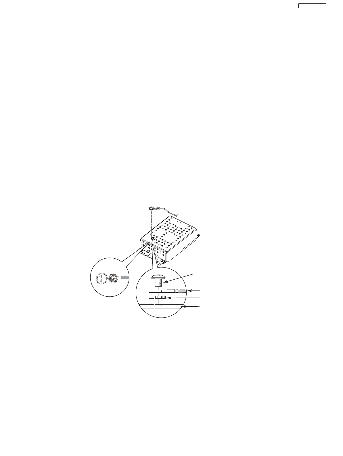
For safety, before closing the lower cabinet, please make sure of the following precautions.
1. The “ground” lead is fixed with the screw.
2. The AC connector is connected properly.
Screw
Terminal of Harness
Washer
Plate Cover SMPS
5
UF-5500 / 4500
1.3. Personal Safety Precautions
1.3.1. Moving Sections of the Unit
Be careful not to let your hair, clothes, fingers, accessories, etc., become caught in any moving sections of the unit.
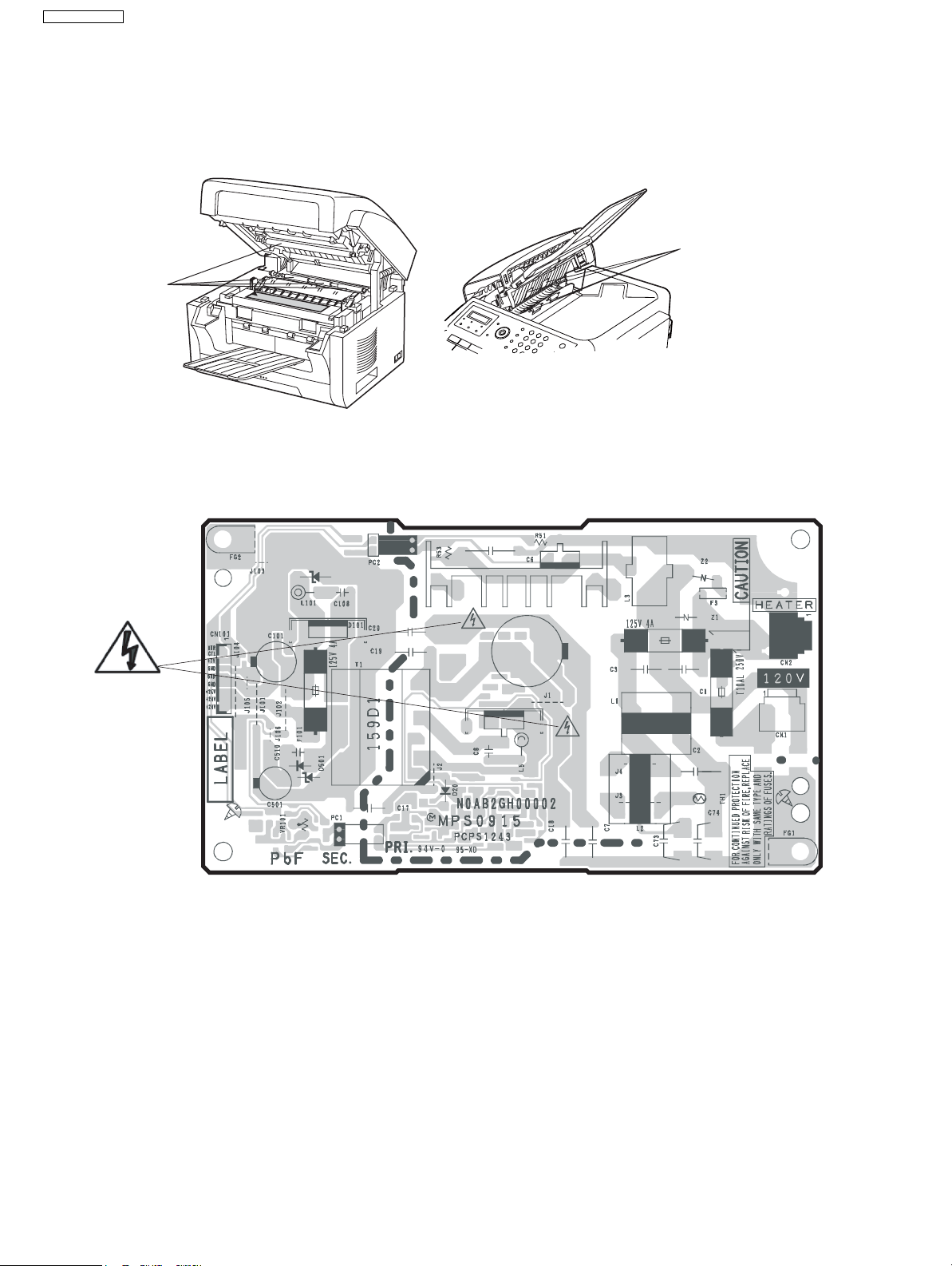
The moving sections of the unit are the rollers and a gear. There is a separation roller and a document feed roller which are rotated
by the document feed motor. A gear rotates the two rollers. Be careful not to touch them with your hands, especially when the unit
is operating.
Feeder Rollers
Rollers
1.3.2. Live Electrical Sections
CAUTION:
When servicing, never disassemble the unit with the AC power cord connected.
Live AC voltage is supplied to the primary side of the power supply unit.
SCR51
D104
F2
C5
Q1
D503
F1
1.4. Service Precautions
1.4.1. Precautions to Prevent Damage from Static Electricity
Electrical charges accumulate on a person. For instance, clothes rubbing together can damage electric elements or change their
electrical characteristics. In order to prevent static electricity, touch a metallic part that is grounded to release the static electricity.
Never touch the electrical sections such as the power supply unit, etc.
6
UF-5500 / 4500
w
2Warning
2.1. About Lead Free Solder (PbF: Pb free)
Note:
In the information below, Pb, the symbol for lead, will refer to standard solder or solder that contains lead.
We will use PbF solder when discussing the lead free solder used in our manufacturing process which is made from Tin, (Sn),
Silver, (Ag), and Copper, (Cu).
This model, and others like it, manufactured using lead free solder will have PbF stamped on the PCB. For service and repair
work we suggest using the same type of solder although, with some precautions, standard Pb solder can also be used.
Caution
• PbF solder has a melting point that is 50° ~ 70° F, (30 ° ~ 40°C) higher than Pb solder. Please use a soldering iron with temperature control and adjust it to 700° ± 20° F, ( 3 70 ° ± 10°C). When using high temperature soldering iron, please be careful not to
heat for too long.
• PbF solder will tend to splash if it is heated much higher than its melting point, approximately 1100°F, ( 6 00°C).
• If you must use Pb solder on a PCB manufactured using PbF solder, remove as much of the original PbF solder as possible and
be sure that any remaining is melted prior to applying the Pb solder.
• When applying PbF solder to double layered boards, please check the component side for excess which may flow onto the
opposite side (See figure, below).
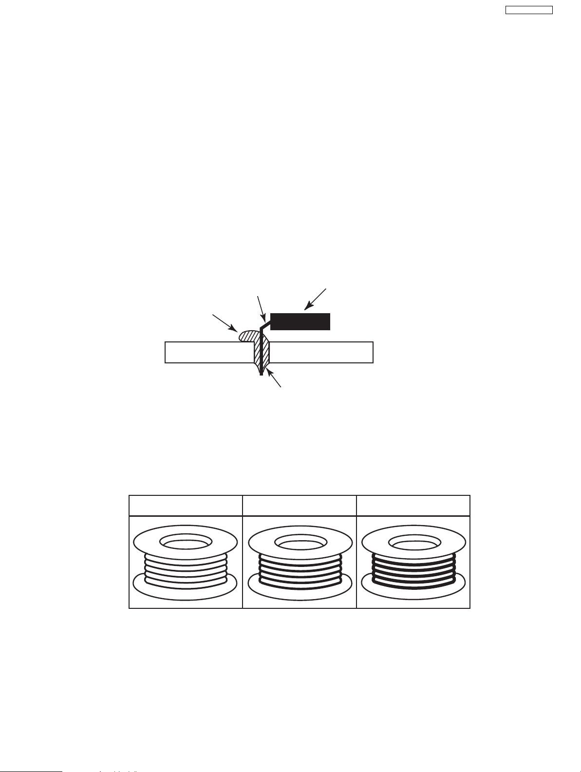
Remove all of the
excess solder
Component
pin
Component
Sliced vie
Solder
2.1.1. Suggested PbF Solder
There are several types of PbF solder available commercially. While this product is manufactured using Tin, Silver, and Copper,
(Sn+Ag+Cu), you can also use Tin and Copper, (Sn+Cu), or Tin, Zinc, and Bismuth, (Sn+Zn+Bi). Please check the manufacturer’s specific instructions for the melting points of their products and any precautions for using their product with other
materials.
The following lead free (PbF) solder wire sizes are recommended for service of this product: 0.3mm, 0.6mm and 1.0mm.
0.3mm X 100g
0.6mm X 100g 1.0mm X 100g
7
UF-5500 / 4500
2.2. Disposing of the P. C. Board
When disposing of a P. C. Board, delete all personal information such as telephone directory and caller list or scrap the P. C. Board.
2.3. Insulation Resistance Test
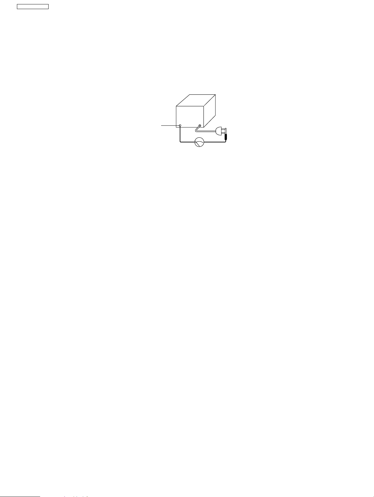
1. Unplug the power cord and short the two prongs of the plug with a jumper wire.
2. Turn on the power switch.
3. Measure the resistance value with an ohmmeter between the jumpered AC plug and each exposed metal cabinet part
(screw heads, control shafts, bottom frame, etc.).
Note: Some exposed parts may be isolated from the chassis by design. These will read infinity.
4. If the measurement is outside the specified limits, there is a possibility of a shock hazard.
Exposed
metal
part
Ohmmeter
Resistance = more than 10MΩ(at DC 500 V)
2.4. Battery Caution
CAUTION
Danger of explosion if battery is incorrectly replaced. Replace only with the same or equivalent type recommended by the manufacturer. Discard used batteries according to following caution.
Disposal of lithium batteries should be performed by permitted, professional disposal firms knowledgeable in state government
federal and local hazardous materials and hazardous waste transportation and disposal requirements.
A battery continues to have no transportation limitations as long as it is separated to prevent short circuits and packed in strong
packaging.
Commercial firms that dispose of any quantity of lithium cells should have a mechanism in place to account for their ultimate disposition. This is a good practice for all types of commercial or industrial waste.
NOTICE: (only for California in the United States)
This product contains a CR Coin Cell Lithium Battery which contains Perchlorate Material special handling may apply.
See www.dtsc.ca.gov/hazardouswaste/perchlorate
Recommend Type Number:
CR2354(BAT300) Manufactured by Panasonic
8
UF-5500 / 4500
2.5. Laser Beam and Fuser Unit Section
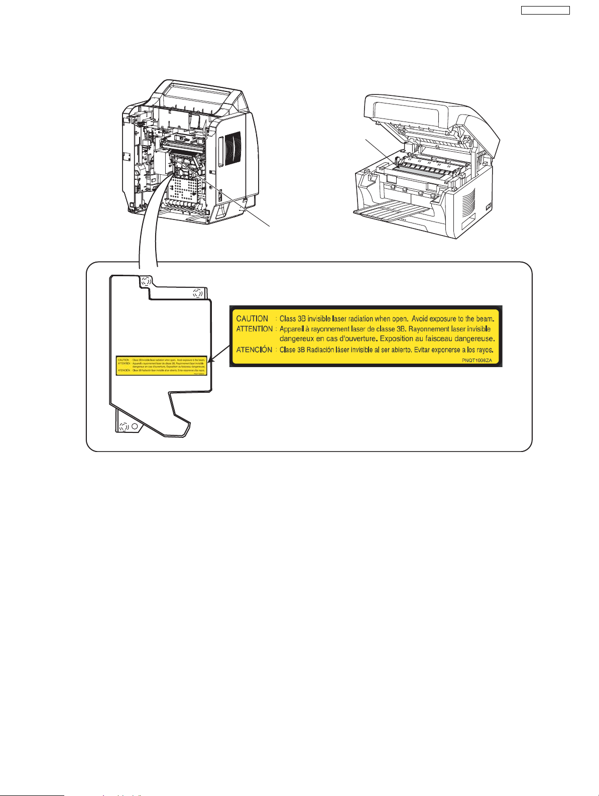
• The printer of this unit utilizes a laser. Use of controls or adjustments or performance of procedures other than those specified
herein may result in hazardous radiation exposure.
• The fuser unit is inside of the unit and gets hot. Do not touch it when removing the jammed paper or cleaning the lower glass.
Fuser Unit
Laser Scanning Unit
* In case of this figure, this Laser Caution Label is located on the other side of the LSU.
2.6. Note for Repairing
Caution
Please inform users of the danger of data being lost at the time of repair.
Data will be lost in the following situations.
1. When replacing the ROM assembly.
2. When replacing the Main board assembly.
3. When executing the Sipment Set.
There is a possibility of data loss in the following situations.
1. When removing a board.
2. When writing new software to ROM.
9
UF-5500 / 4500
3 Specifications
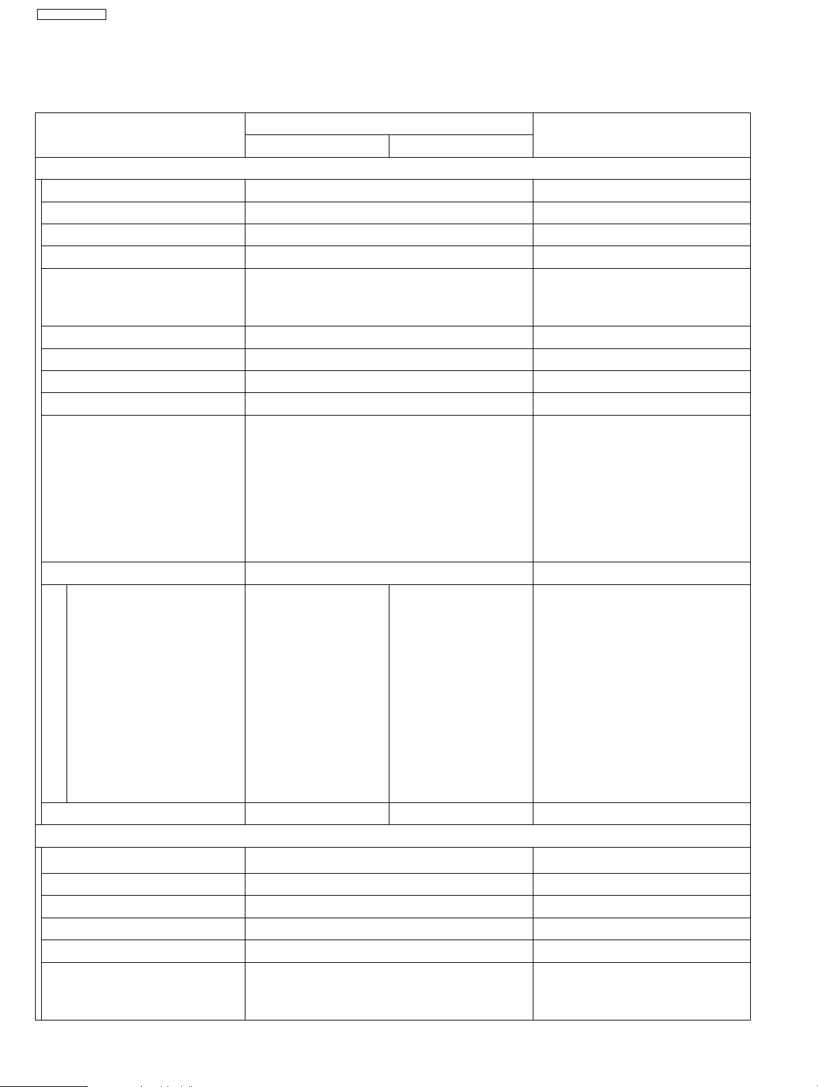
3.1. Fax Function
Items
Remarks
UF-5500 UF-4500
Main Specifications
1 Compatibility G3 ITU-T Std. & Non-Std.
2 PSTN Line Port Yes
3 Leased Line Port No
4 V.24 Line Port No
33.6 / 31.2 / 28.8 / 26.4 / 24.0 / 21.6 / 19.2
Description
5 Modem Speed
/ 16.8 / 14.4 / 12.0 / 9.6 / 7.2 / 4.8 / 2.4
kbps
6 Coding Scheme MMR/MR/MH
7 ECM Yes Conforms to ITU-T
8 Short Protocol Yes (B, D)
9 Transmission Speed Approx. 3 second ITU-T Image No. 1 / A4 / Std
Transmission
Std 8 x 3.85
10 Communication
Resolution
(pels / mm x lines / mm)
Fine 8 x 7.7
S-Fine 8 x 15.4
Reception
Std 8 x 3.85
Fine 8 x 7.7
S-Fine 8 x 15.4
11 Multi Function
[USB]
Printer
Scanner
PC-Fax
Machine Setting
Status Monitor
Yes ( GDI )
Yes ( TWAI N)
Yes
Yes
Yes
No
No
No
No
No
[LAN]
Printer
Scanner
PC-Fax
Machine Setting
Status Monitor
Yes ( LP R)
Yes
(Original Mode)*
Yes
Yes
Yes
No
No
No
No
No
*Scan to PC
12 Multi Function Interface USB2.0 / LAN N/A
Scanner Mechanism
ADF Capacity 30 sheets
1
A4 / Letter & 60g/m
2
(16lb)
2 Document Size (Max.) 8.5 x 23.6 in (216 x 600 mm)
3 Document Size (Min.) 5.0 x 5.8 in (128 x 148 mm)
4 Effective Scanning Width 8.3 in (212 mm) Letter size
5 Scanning Device CIS
Scanning Resolution
6
(pels / mm x lines / mm)
Std 8 x 3.85
Fine 8 x 7.7
S-Fine 8 x 15.4
10
UF-5500 / 4500
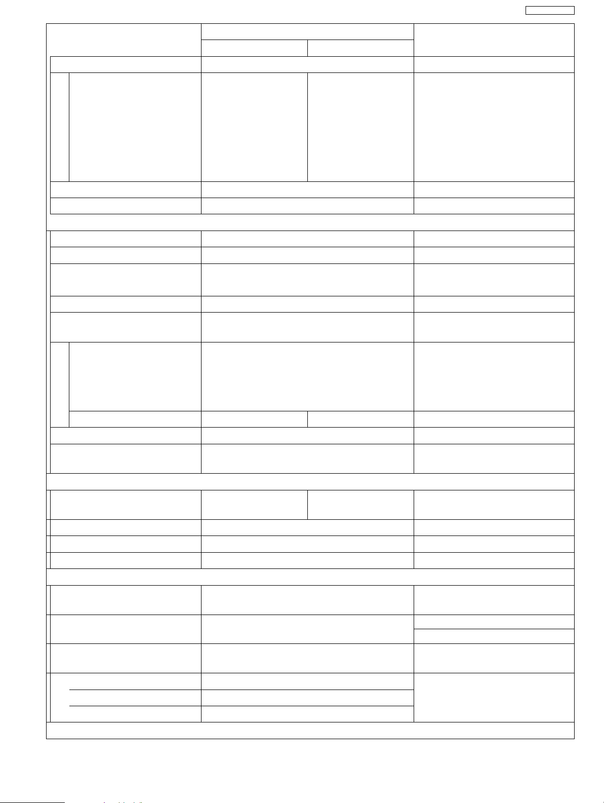
Items
Remarks
UF-5500 UF-4500
7 Scanning Speed For Fax / Approx
Letter sized document
Description
2.8 sec. Standard
2.8 sec. Fine
6.3 sec. S-Fine
4.2 sec. Standard
4.2 sec. FIne
7.1 sec. S-Fine
A4 sized document
2.9 sec. Standard
2.9 sec. Fine
6.7 sec. S-Fine
4.3 sec. Standard
4.3 sec. Fine
7.8 sec. S-Fine
8 Reduction XMT No
9 Collation Stack Yes
Printer Mechanism
1 Recording Method LP
2 Recording Paper Size A4 / Letter / Legal* *Legal cassette is option
3 Recording Paper
Capacity
250 sheets
A4 / Letter / Legal, (20 lb /
2
75 g/m
) paper (note 1)
4 Effective Printing Width 8.2 in (208 mm) Letter size
5 Recording Resolution
Copy, Fax
203 x 391 dpi (Fax : S-Fine)*
203 x 196 dpi (Fax : Fine)*
203 x 98 dpi (Fax : STD)*
The size of page-memory is
5.5MB.(600dpi Legal size)
*The print resolution expands
to 600 x 600dpi.
203 x 391 dpi (Copy : S-Fine)*
203 x 196 dpi (Copy : Fine)*
PC Printing Data 600 x 600 dpi No
6 Recording Speed 24 ppm
7 Collation Stack Yes
Recorded paper output is
facedown.
Memory / Clock
Document Memory
1
Capacity
480 pages (8 MB)
240 pages (Approx
4 MB)
ITU-T Image No.1
(A4, STD. Resolution)
2 Memory Backup Yes
3 Document Memory Type Flash Memory
4 Clock Backup 5 years
Copy Quality
1 Halftone (Tx) Yes
2 Super Fine (Tx & Rx)
8 x 15.4
64-Level Error Diffusion
Quality mode only
(dot / mm x line / mm)
3 Original Contrast
Selection (Tx)
Yes 3-Levels
4 Smoothing (Rx)
Fax, Copy No
With Auto Picture / Text
Recognition
PC Printing Data No
Power Supply
11
UF-5500 / 4500
Items
Description
UF-5500 UF-4500
1 Power Requirement 120 VAC, 60 Hz, Single Phase
2 Power Consumption
Standby
ES=On 5.5 Wh
Reception 500 W
Copy 500 W
Maximum 950 W
Environment
1 Temperature
Operation 50 to 90.5 °F (10 to 32.5 °C)
Storage 32 to 104 °F (0 to 40 °C)
Transport (Max. 72 H) 32 to 104 °F (0 to 40 °C)
2 Relative Humidity
Operation 20 to 70 % RH
Storage (Max. 120 H) 20 to 80 % RH
Transport (Max. 120 H) 20 to 80 % RH
Standards
UL60950-1
1 Safety
2nd Edition,2007-03-27 (AC)*
CSA C22.2 No.60950-1-07 (AC)*
2 PSTN
3EMI
FCC Part68/IC.CS-03 (AC)* *Canada only
Class B computing device
in FCC Part 15 Subpart B
FCC Part 68
Construction
1 Dimensions (W x D x H)
Approx. width 16.5 x depth 18 x heght
11.7 in (420 mm x 457 mm x 297 mm)
2 Weight (Excluding paper) Approx. 27.8 lb (12.5 kg)
Attachment & Accessories
Toner Cartridge
Drum Cartridge
User’s Guide
Power Cord
Tel Line Cable
Document Trays (RX)
Document Trays (TX)
CD-ROM
Yes (1)*
Yes ( 1)
Yes ( 1)
Yes ( 1)
Yes ( 1)
Yes ( 1)
Yes ( 1)
Yes (1)*
Yes (1)*
Yes ( 1)
Yes (1)
Yes ( 1)
Yes ( 1)
Yes ( 1)
Yes ( 1)
Yes ( 1)
Consumables
1 Process Type Separate (2 pieces)
Toner Yield
2
3% Black Chart
(ITU-T Image No. 1
Approx. 3,000 sheets
Chart)
3 OPC Yield Approx. 6,000 sheets
Remarks
ES: Energy Saver
*Canada only
*Canada only
Excluding projections and
Optional Paper Cassette.
Including starter consumable
supplies.
*Yield 500 sheets as a starter
Specified countries only
*Include PC software
Multiple copy mode Operation
Environment 73.4 °F (23°C),
50%RH, using A4 paper.
12
UF-5500 / 4500
Items
Remarks
UF-5500 UF-4500
4 Toner Warning Sensor Yes Magnetic Field Sensor
Description
Toner Cartridge
5
(Panasonic Brand Name)
Drum Cartridge
6
(Panasonic Brand Name)
Yes
Yes
Options
1 Cassette & Deck Yes Legal Paper Cassette
2 IC Memory No
3 Page Memory No
4 Battery Backup 72 hours No
5 G3 Optional
Communication Port
No
6 Handset No
7 V.24/Encryption Interface No
8 PDL No
9 PC Interface
Printer Interface (GDI) Standard No
Scanner Interface* Standard* No *USB (TWAIN), LAN (LPR)
Class 2 Interface No No
PC-Fax Standard* No *Panafax Desktop
Document Manager* Standard* No *Quick Image Navigator
MFP Utilities* Standard* No *Status Monitor
Languages
Control Panel
Function Label
LCD Display
Printouts
Operation Instruction
English (AU), English/C-French (AC)
English (AU), English/C-French (AC)
English / C-French / Spanish
English / C-French / Spanish
English (AU)*, English/C-French (AC)
Can be selected by setting.
Can be selected by setting.
Provide by CD-ROM.
*Only an initial lot.
Quick Installation Guide
Important Information
English (AU), English/C-French (AC)
(Illustration)
Illustration only.
Guide
Dual Operation
1 Multi Task Operation Yes
2 Direct XMT Reserve Yes
3 Memory XMT Reserve Yes
4 Number of Memory Job
Files
20 files 10 files
Dialing/Telephone Features
1 One-Touch Keys 32 (16 x 2)
2 One-Touch / Program
Keys
3
Lower SW /w LED Lamp Yes
32 (16 x 2)
Upper / Lower switching
operation
Upper / Lower switching
operation
13
UF-5500 / 4500
Items
Remarks
UF-5500 UF-4500
Description
4 One-Touch Auto Dialers 32
Upper / Lower switching
operation
5 Abbr. Auto Dialers 168
Total Auto Dialing
6
Locations (Max.)
Digits of Tel Number
7
(Max.)
8 Digits of Station Name
(Max.)
200
36
15
9 Directory Search Dialing Yes With Directory Search Key
10 Full Number Dialing
(Buffered Dialing)
11 Direct Dialing
(Monitor Dialing)
Yes* *Max. 10 stations
Yes Voice mode (note 4)
12 Automatic Redialing Yes
13 Manual Redialing Yes
14
Chain Dialing Yes On Monitor Dialing mode only
15 Line Monitor Speaker Yes
16 Pulse / Tone Dialing Yes
17 Pulse to Tone Change Yes
18 Flash Key Yes
19 External Telephone Jack 1 (No Off-hook detection) External Telephone
Transmission Features
1 Direct Transmission Yes ADF Transmission
2 Memory Transmission Yes Page Retransmission
3Quick Memory
Transmission
4 Multi-Station
Transmission (Max.)
Yes
210
Max. 210 stations
5 Multifile Transmission No
6 Direct Deferred
Transmission
7 Deferred Memory
Transmission
8 Deferred Multi-Station
Transmission
9 Priority Direct
Transmission
10 Priority Memory
Transmission
No ADF Deferred Transmission
Yes
Yes
Yes Priority ADF Transmission
No
11 Batch Transmission No
Reception Features
1 Substitute Reception Yes
*A4 / LTR : 72 - 100%,
2 Fixed Reduction Yes*
LGL : 80 - 100% (1% Steps),
Top & Center Alignment
14
UF-5500 / 4500
Items
Remarks
UF-5500 UF-4500
*A4 / LTR : 72 - 100%,
Description
3 Auto Reduction Yes*
LGL : 80 - 100% (1% Steps),
Top & Center Alignment
4 Overlapping Print Yes
Page End Approx. 0.39 in
(10 mm)
5 Receive to Memory Yes Print with Password
6 Distinctive Ring Detector
(DRD)
Yes
Receive Control
1 Fax / Tel Auto Switch Yes
2 Silent Reception No
3 External TAM Interface Yes
4 Remote Reception Yes (DTMF)
Polling Features
1 Polling Yes
2 Turnaround Polling No
Multi-Station Polling
3
(Max.)
210 Max. 210 stations
4 Deferred Polling Yes
5 Deferred Multi-Station
Polling
Yes
6 Direct Polling Tx No
7 Memory Polling Tx Yes 1 File
8 Preset Polling Password Yes
9 Temporary Polling
Password
10 Continuous Polling Yes
Yes
Select by Function Parameter
"003:Continuous Poll".
Convenience
1 Panel Display Yes 16 x 2 Alphanumeric LCD
2 Voice Contact No
3 Edit File Mode Yes
Delete Operation : press
[STOP] key.
4 Incomplete File Save Yes
5 Automatic Cover Sheet Yes
Copy Features
1 Multiple Copy Yes Multi Sort Copy only
2 Reduction Copy Yes
Copying Resolution
3
(dot / mm x lines / mm)
203 x 391 dpi (Copy : S-Fine)
203 x 196 dpi (Copy : Fine)
Certainty
1 Verification Stamp No
2 Header / Total Page Print Yes
15
UF-5500 / 4500
Items
Remarks
UF-5500 UF-4500
Description
3 Transaction Journal Yes
32 Transactions / with View
Mode
4 Comm. Journal Yes With Image
5 Last Ind. XMT Journal Yes
6 Power Failure Report No
List Printouts
1 One-Touch List Yes
2 Abbr. No. List Yes
3 Program List Yes
4 Directory Search List Yes
5 Fax Parameter List Yes
6 File List Yes
7 Character Code List No
8 Directory Sheet Yes No
Identifications
1 Logo Yes 25 Characters
2 Multiple Logo Yes
3 Character ID Yes 16 Characters
4 Numeric ID Yes 20 Digits
Special Communications
1 Password XMT / RCV Yes Closed Network
2 Select Reception Yes TSI Check
3 Relay XMT Request No
4 Relay XMT Center No
5 Confidential XMT /
Polling
No
6 Confidential Center No
7 Mailbox XMT / Polling Yes
8 Mailbox Center Yes (10 Box)
9File XMT No
10 Fax Forward Yes Received File Transfer
11 NYSE Feature Yes
12 Sub-Address XMT Yes T. Routing
13 Sub-Address RCV No
14 OMR-XMT No
For use with Mark Sheet
transmission
Others
1 Fax Access Code Yes
2 PIN Code Access Yes PBX Access Code
3 Intelligent Redial Yes 2 Files
4 Department Code Yes
5 Power Saver Mode Yes
6 Day Light Time Save Yes
7 Self Diagnostic Function Yes
16
UF-5500 / 4500
Items
Remarks
UF-5500 UF-4500
Description
8 Remote Diagnostic
Function
Yes
9 Check & Call Function Yes Same us UF-6200
10 Job Build Yes
Junk Fax Reception Filter
11
(Numeric ID)
Yes
12 Direct Dial Prohibition Yes
13 Direct Dial Re-entering Yes
Warning for Important
14
Destination
No
15 Multi-station Prohibition Yes
Warning for Multi-station
16
Transmission
Yes
17 Black-list from Caller ID No
18 Multiple fax print function Yes
New misdial prevention
19
function
Yes
Change panel operation
sequence
PC Application Software
[USB]
Document Scanner
CD-ROM
Yes ( CF P)
CD-ROM (same as
UF-5500)*
No
*CD-ROM is common to both
models, and includes the Oper-
ating Instructions.
(TWAIN Driver)
Quick Image Navigator
GDI Printer Driver
Configuration Editor
Phone Book Editor
Panafax Desktop
Status Monitor
Yes
Yes ( CF P)
Yes ( CF P)
Yes ( CF P)
Yes ( CF P)
Yes ( CF P)
No
No
No
No
No
No
[LAN]
Communications Utility
Quick Image Navigator
GDI Printer Driver
Network Configuration
Editor
Network Address Book
Editor
Panafax Desktop
Device Explorer /
Yes (
Original Mode
Yes (same as USB
App)
Yes ( LP R)
Yes (FTP)
Yes (FTP)
Yes*
Yes (SNMP / MIB)
)
No
No
No
No
No
No
*/w Fax Driver
No
No
Device Monitor
Scanner Function
1 Color Scan Yes No
2 Scan Mode
Network Scanner
3
Address
B&W, Gray Scale,
Color
N/A
Auto IP Ditect Only N/A
17
UF-5500 / 4500
Items
Description
UF-5500 UF-4500
600 x 600 dpi (Opt)
4 Scan Resolution
300 x 300 dpi (Opt)
200 x 200 dpi (Opt)
N/A
100 x 100 dpi (Opt)
Firmware Update / Download
1 Remote Update Yes
2 Local Update
Memory Card (FROM) No
Parallel Port No
USB Yes
Network
Yes* No *FTP, using the Network
3 Download to FROM Card No
Machine Life
1 Machine Life 60 K or 5 years whichever comes first.
Noise Level (dB)
2
Stand-by
Working
Below 42dB
Below 63dB
Remarks
ITU-T T3/T4 (using Remote
Firmware Update Tool)
Using the Local Firmware
Update Tool.
Firmware Update Tool.
Note:
1. Paper Cassette Configuration
• A4 : 210mm x 297mm
• Letter : 8.5” x 11”
• Legal : 8.5” x 14” (13” Legal {8.5” x 13”} is not supported.)
2. Paper Specifications
The Panasonic standard paper was used for stack testing; 75g/m
3. Paper Specifications
The Panasonic standard paper was used for stack testing; 60g/m
4. Monitor Dialing Mode
Press START to initiate Fax communication. Automatic Redialing is not available.
2
A4/Letter/Legal.
2
A4/Letter/Legal.
18
3.2. Printer & Scanner Function (UF-5500 only)
UF-5500 / 4500
Items
Description
UF-5500
Remarks
Interface
1 USB Port Standard
Printer Function
1 Printing Size Letter / A4 / Legal* *Legal cassette is an option
2 Bypass No
3 Stapling No
4 Printing Resolution 600 dpi
5OS
Win 2000 / XP / Server 2003 /
Server 2008 / Vista / 7
6GDI Yes
7 PDL (PCL6) No
8 PDL (PostScript 2) No
9 Duplex Printing No
10 Collation Stack Yes
11 Status Monitor Yes Local Connection
12 Network Printing Yes
13 Network Status Monitor Yes
14 Smoothing No
15 Applicable PC IBM PC, AT or Compatible
16 Multi-Task Operation
Printing while Fax-XMT
from Memory
Printing while Fax-RCV
into Memory
Fax-XMT from Memory
while Printing
Fax-RCV into Memory
while Printing
17 Output to Separate Tray
for Printing, Fax, Copy
Yes
Yes
Yes
Yes
No
18 Font No
19 Security Print No
Scanning Function
1 Halftone Yes
64 Level Error Diffusion
Quality Mode only
2 Color Yes
3 Scanning Width 8.3 in (212 mm)
4 Scanning Resolution 600 dpi
5 Driver TWAIN (USB)
6 2-Sided Scanning No
19

UF-5500 / 4500
4 General/Introduction
4.1. Optional Accessories
Model No. Description Specifications
UE-409100 Legal Cassette 1 Legal cassette
UG-5591
UG-5590
*1
Prints about 3,000 pages. (See Note 1)
*2
Prints about 6,000 pages. (See Note 2)
Replacement toner cartridge
Replacement drum cartridge*
cartridge is replaced, it is necessary to install a
new toner cartridge simultaneously.)
Note:
1. Average yield is based on 3% coverage of the printable area with repetitive printing of continous printing(Letter/A4 size, single
side printing, default density). The yield of a Toner Cartridge varies depending on the coverage, temperature, humidity, media,
etc. Therefore, the average yield cannot be guaranteed.
2. A4 portrait in single-sided, printing 3 pages per print job. The yield of the drum cartridge when printing 1-page per print job, will
decrease to about half compared with printing 3-pages per print job. The yield of a Drum Cartridge varies depending on the
coverage, temperature, humidity, media, etc. Therefore, the average yield cannot be guaranteed.
*1
2
(When the drum
1 Toner cartridge
1 Drum cartridge
20

UF-5500 / 4500
5 Hardware Requirements for Printer Driver and Application
Software
To use Panasonic Document Management System on your computer, the following are required:
Operating System:
Windows
Windows® XP (32/64-bit) (Service Pack 2 or later)
Windows Server® 2003 (32/64-bit) (Service Pack 1 or later)
Windows Vista® (32/64-bit)
Windows Server® 2008 (32/64-bit)
Windows® 7 (32/64-bit)
Hardware:
IBM
(CPU Intel® Pentium® 4 1.6 GHz or more recommended)
RAM:
Windows 2000: 256 MB or more
Windows XP: 512 MB or more
Windows Server 2003: 512 MB or more
Windows Server 2008: 1 GB or more
Windows Vista: 1 GB or more
Windows 7: 1 GB or more
Other Hardware:
CD-ROM drive
Hard disk drive with at least 300 MB of available space
USB interface (USB 2.0)
LAN interface (10Base-T/100Base-TX)
Other:
Internet Explorer
Warning:
• To assure continued emission limit compliance:
- use only shielded USB cable (Example: Hi-Speed USB 2.0 certified cable).
- use only shielded LAN cable (category 5 straight cable).
• To protect the unit, use only shielded USB cable in areas where thunderstorms occur.
Note:
• A USB cable is not supplied. Please purchase a shielded Type-A male/Type-B male USB cable.
®
2000 (Service Pack 4 or later)
®
PC/AT® and compatibles
®
6.0 (Service Pack 1 or later)
21
UF-5500 / 4500
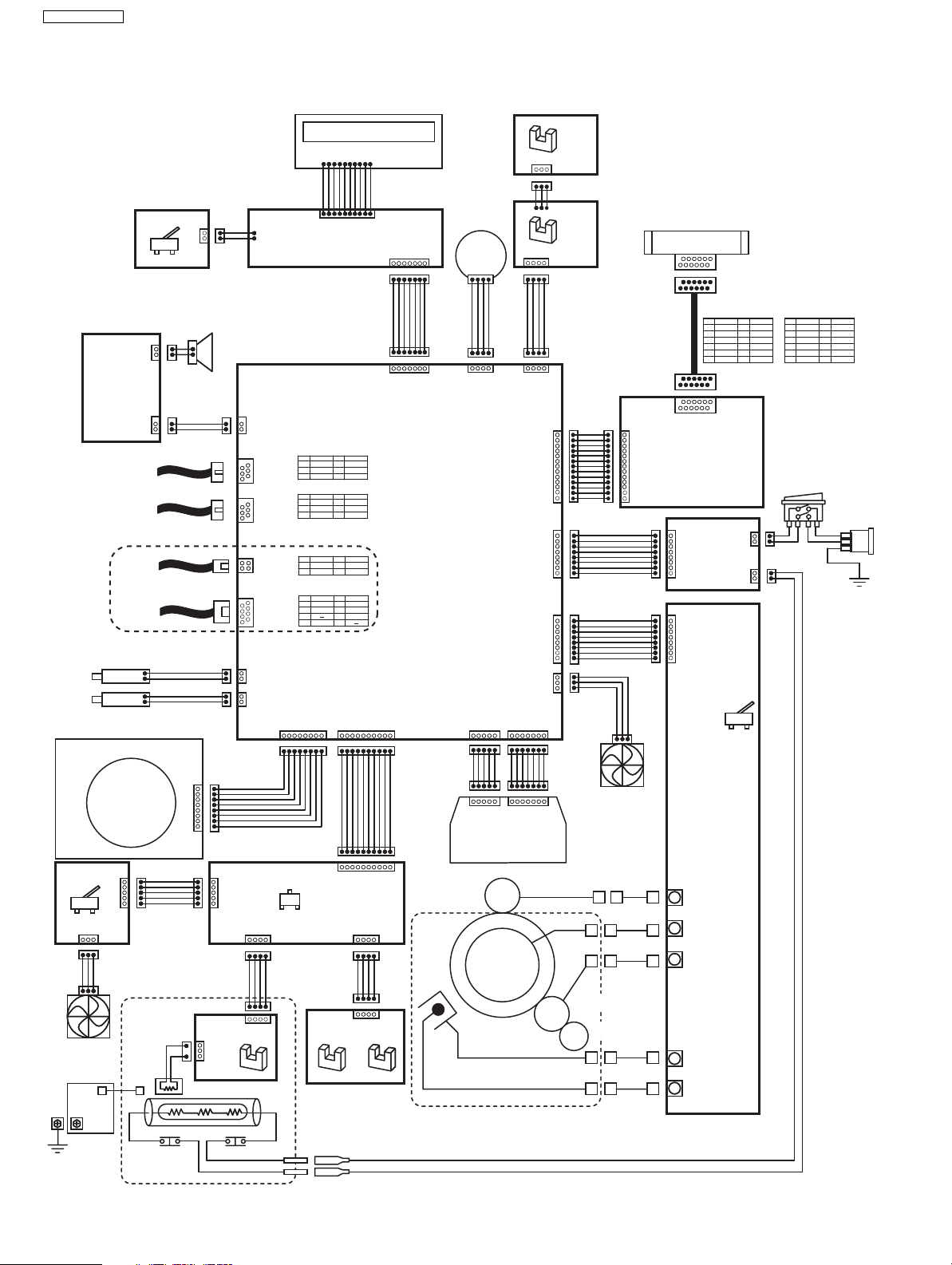
6 Technical Descriptions
6.1. Connection Diagram
REGISTER
SOLENOID
PICKUP
SOLENOID
DC MOTOR UNIT
MOTOR
TELEPHONE
LINE
EXTERNAL
TELEPHONE
MAIN
ADF DOOR
SENSOR
121
2
CN57
CN54
212
1
TO
TO
TO
PC/USB
TO
PC/LAN
UF-5500 only
SW51
LCD
DB6
E
R / WRSV0
VDD
DB7
CN3
CN1
OPERATION PANEL BOARD
SP+
Speaker
SP-
CN201
SPSP+
REG
DG
PICK
DG
1
1
2
2
3
3
4
4
5
5
6
6
7
7
8
8
CN100
CN101
CN300
CN750
CN514
CN507
212
1
CN100
1
1
2
2
3
3
4
4
5
5
6
6
CN101
1
1
2
2
3
3
4
4
5
5
6
6
CN300
1 4
1 4
2 3
2 3
CN750
1
2
3
4
5
6
5
7
8
121
2
121
2
123456781234567
8
24V
CLK
BRAKE
24V
DGDGLD
SS
VSS
DB5
DB4
987654321
987654321
10
CN2
MAIN BOARD
NAMENAMENo
NAMENAMENo
2NoE(G) / A2a11
2NoE(G) / A2a11
b / B14a / A13
b / B14a / A13
b16S(W) / B25
b16S(W) / B25
NAMENAMENo
NAMENAMENo
2NoS(W)b11
2NoS(W)b11
a / A14b / B13
a / A14b / B13
a16E(W)5
a16E(W)5
NAMENAMENo
NAMENAMENo
2NoD-VBUS1
2NoD-VBUS1
4
GNDD+3
4
GNDD+3
NAMENAMENo
NAMENAMENo
2NoTD-TD+1
2NoTD-TD+1
TCT4RD+3
TCT4RD+3
RD-65
RD-6
8RCT7
8RCT7
CN508
123456789
123456789
123456789
PTOP
POUT5VTHRM1
GND
PICK
FANON2
FANDET2
TNR
1234567123456
THRM
THRM
1234567123456
10
10
10
REG
ADF
7
MOTOR
ABXA
CN701
CN701
POLCLK
123
123
123451234
XREADY
XB
4
4
5
POLON
DG
XHSYNC
24V
KSTART
KSCLK
OPERST
KSTART
KSCLK
OPERST
KTXD
DG
5V
KTXD
DG
5V
7
CN511
LSU
3.3V
CN700
CN700
CN500CN501CN502
1234567123456
DG5VXAPC
DOCUMENT
SENSOR
PS54
123
CN69
READ
POSITION
SENSOR
PS53
123
4
CN56
RPS
DG
DOCU
123
4
123
4
CN510
SIG
1
1
GND
2
2
3.3V
3
3
VREF
4
4
GND
5
5
SI
6
6
GND
7
7
CLK
8
8
VLED
9
9
LED_G
10
10
LED_R
11
11
LED_B
12
12
CNT
13
CN504
HTRCTL
1
1
7V
2
2
DG
3
3
DG
4
4
DG
5
5
24V
6
6
24V
7
7
24V
8
CN505
CVR
1
1
HVERR
2
2
TRS
3
3
DEV
4
4
CHG
5
5
GND
6
6
NC
7
7
24V
8
CN506
DG
1
1
FANDET1
2
2
FANON1
3
3
7
XLDEN
DG
XVIDEO
DC FAN1
CN59/CN79
(Left )
1
1
2
2
3
3
4
4
5
5
6
6
7
7
8
8
9
9
10
10
11
11
12
12
13
CISMODULE
CN61 (UF-5500)
12 11
12 11
CN61(UF-5500)
CN71(UF-4500)
CIS RELAY
BOARD
CN101
1
1
2
2
3
3
SMPS
4
4
5
5
6
6
7
7
8
CN1
1
1
2
2
3
3
4
4
5
5
6
6
7
7
8
COVER OPEN SW
CN71 (UF-4500)
NAMENAMENo
No NAMENAMENo
2NoDGSIG1
VREF43.3V3
SI6CNT5
CLK8DG7
LED_G10VLED9
12
LED_BLED_R11
2 1
2 1
LED_B
1
LED_G
11
No
No NAMENAMENo
2
43
CLK DG
65
SI
87
VREF
109
DG
12
NAMENAMENo
LED_R
VLED
CNT
3.3V
SIG
POWER SW
CN1
121
2
CN2
HEAT
121
LAMP
2
LIVE
NEUTRAL
AC INLET
SW1
HVPS
CN63
PICKUP
SENSOR
SW50
DG
DC FAN 2
(Right )
VARISTOR
BOARD
CN65
1234123
TONER
SENSOR
4
123456789
123456789
123456789
10
10
10
CN64
IC51
CN66
1234123
4
TRANSCRIPTION
ROLLER
OPC
DRUM
TRA
OPC
CN51
1
1
2
2
3
3
4
4
5
5
12312
3
DG
PICK
DG
FANDET2
FANON2
CN67
1
1
2
2
3
3
4
4
5
5
DEV
5V
PTOP
DG
CN50
REGISTER
SENSOR
PS51 PS52
REG
1234123
4
PTOP
SENSOR
SCOROTRON
DRUM UNIT
DEVELOPING
ROLLER
TONER SUPPLY
ROLLER
GRID
CHG
THRM15VPOUT
FANDET2
FANON2
GND
FUSER
123
UNIT
THRM1
DG
CN52
1
1
2
2
3
3
THERMISTOR
CN53
EXIT SENSOR
PS50
4
HEAT LAMP
THERMOSTAT THERMOSTAT
22

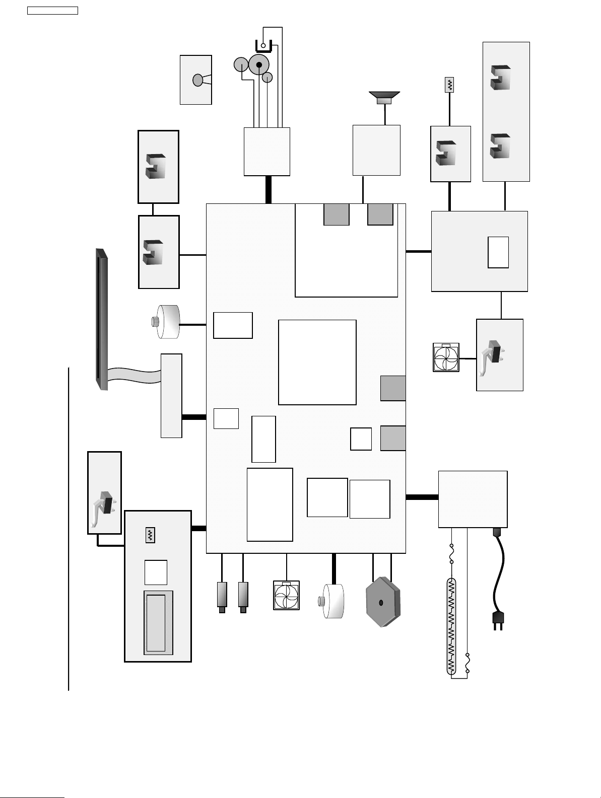
6.2. General Block Diagram
MAIN UNIT
SOC (IC300)
This custom IC is used for general MFP operations.
1) CPU ARM9 operating at 250MHz.
2) SDRAM Controller Controls SDRAM Memory.
3) USB Controller with PHY Apply to USB2.0 HS
4) Scanner I/F Controls the CIS and AFE, and process the scan images.
5) LSU I/F Controls the polygon motor and outputs the VIDEO signal to LSU.
6) MOTOR I/F Controls the DC motor and Stepping Motor.
7) FAN I/F Controls FAN MOTOR and detect the rotation of FAN MOTOR.
8) OPERATION PANEL I/F Serial Interface with Operation Panel.
9) SENSOR I/F Detects the Sensor signal.
10) I/O PORT I/O Port Interface.
11) A/D, D/A converter Sends beep tones, etc.
Convert Analog signals to Digital signals.
12) RTC Real time clock.
13) MODEM Performs the modulation and the demodulation for FAX communication.
14) Analog Front End I/F Controls the DAA device for TEL/FAX function.
15) LAN Controller Ethernet Control.
ROM (IC402)
This 16MB(UF-5500)/8MB(UF-4500) FLASH ROM contains all of the program instructions for the unit operations.
It also supports the User Settings backup and FAX.
UF-5500 / 4500
SYNCHRONOUS DYNAMIC RAM (IC400)
This 256Mbit SDRAM is used for CPU work and receive and page memory.
POWER SUPPLY
DC-DC converters generate 3.3V and 1.2V for system power.
The regulator generates 5V for peripheral devices.
TEL/FAX I/F
Composed of ITS circuit and NCU circuit.
3 ICs called SDAA(Silicon Direct Access Arrangement) control the Telephone line, and Speaker.
READ SECTION
CIS Unit to read transmitted documents.
CIS Unit is connected to CIS RELAY BOARD Unit.
Scan data is converted by AFE(IC503).
MOTOR
This model has 1 DC motor and 1 stepping motor.
IC300 drives the DC motor for printing.
IC700 drive the stepping motor for Auto Document Feeder motor.
LSU
Forms the images on the OPC DRUM by rotating polygon motor and reflecting the laser beam against polygon.
SENSORS
Composed of 3 switches and 5 sensors.
POWER SUPPLY BOARD
Supplies +24V and +7V to the Main unit and controls the Heat Lamp.
HIGH VOLTAGE POWER SUPPLY BOARD
Supplies bias required for the printing operation: bias of the DRUM, Developing and Transcription.
FIXING UNIT
Composed of heat lamp, thermistor and thermostats.
23
UF-5500 / 4500
CIS
Varistor
Speaker
AMP2
HVPS
RP Sensor
AMP8
TEL
UF-5500:600dpi / UF-4500:300dpi
AMP4(Blue)
Document Sensor
JST4
(ADF)
Motor
Color CIS
FFC 12
ADF motor
Driver
EXT
DAA block
Lite
Sirius
SP
AMP2
TEL
AMP10
FAN (right)
USB
2
AMP4
Thermistor
(Heater)
EXIT Sensor
JST3
AMP4
AMR
AMP5
PTOP Sensor
Register Sensor
sensor
Toner Sensor
Pick Up Sensor
ADF
DOOR
Sensor
eries System Schematic
eries System Schematic
S
S
5500/4500
5500/4500
-
-
UF
UF
AMP2
Operation Panel Board
Ope
2Line
Transit
Thermistor
(Room)
G/A
LCD
AFE
AMP13
)
Regratoe
Phy
24V㸢
(256Mbit
SDRAM
5V
7V㸢
FLASH
UF-4500 64Mbit)
(UF-5500 128Mbit/
3.3V/1.2V
DC-DC
LAN
LAN/USB: UF-5500 only
AMP8
(Blue)
SMPS
AC inlet
Main Board
AMP8 or 7
㪬㪝㪄㪌㪌㪇㪇㪑㪋㪍㫂㪼㫐㩿㪋㪣㪜㪛㪀 㪆㩷㩷㪬㪝㪄㪋㪌㪇㪇㪑㪋㪌㫂㪼㫐㩿㪊㪣㪜㪛㪀
JST2
Regist Solenoid
JST2
Pick Up Solenoid
JST3
FAN (left)
JST8
DC motor
AMP7
AMP5
LSU
Thermostat
Heater
Thermostat
24
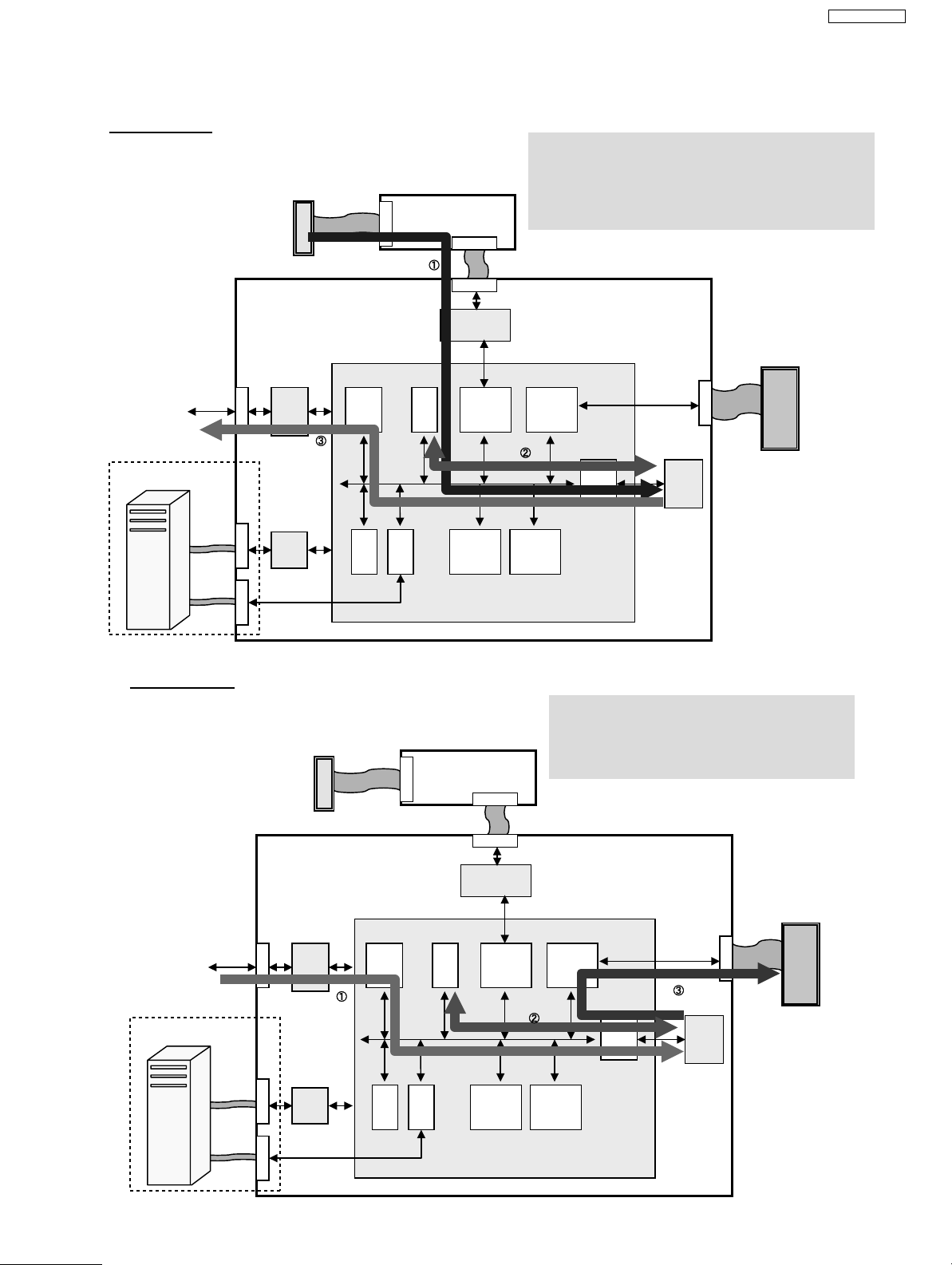
6.3. Main Board Section
6.3.1. Data Flow
[FAX Tx]
CISunit
CIS Relay Board
CN61/71
CN59
UF-5500 / 4500
1. An analog image data is output from CIS unit to IC503.
IC503 decodes the analog data to digital data, and outputs to IC300.
Scanner I/F in IC300 process image data and stores it in IC400
through SDRAM I/F.
2. CPU compresses the data in IC400.
3. CPU transfer the data to MODEM
and outputs it to TEL LINE through DAA circuit.
TEL
LINE
UF-5500 ONLY
PC
LAN
USB
[FAX Rx]
Main Board
IC100
IC101
DAA
CN100
IC750
PHY
CN750
CN300
CISunit
MODEM
LAN
I/F
USB
I/F
CPU
CN61/71
CN510
AFE
Scanner
I/F
CIS Relay Board
CN59
IC503
IC300
DSPJBIG
Print I/F
SDRAM
I/F
CN500
IC400
SDRAM
1. FAX data is input from TEL LINE to MODEM in IC300
through DAA circuit.
And then stored it in IC400 through SDRAM I/F.
2. CPU decompresses the data in IC400.
3. Print I/F retrieves the data from IC400 and outputs it to LSU.
LSU
TEL
LINE
UF-5500 ONLY
PC
LAN
USB
Main Board
IC100
IC101
DAA
CN100
IC750
PHY
CN750
CN300
MODEM
LAN
I/F
USB
I/F
CPU
CN510
AFE
Scanner
25
IC503
IC300
DSPJBIG
Print I/F
SDRAM
I/F
I/F
CN500
IC400
SDRAM
LSU
UF-5500 / 4500
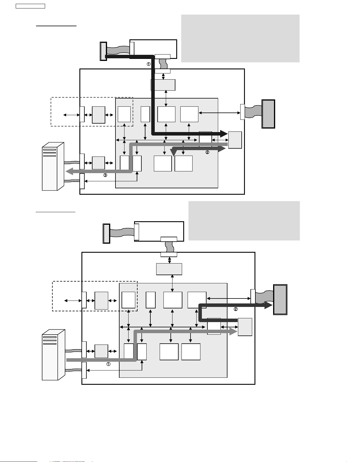
[PC Scan] (UF-5500 only)
CISunit
CN61/71
Main Board
IC100
IC101
PC
TEL
LINE
LAN
USB
CN100
CN750
CN300
DAA
IC750
PHY
MODEM
LAN
I/F
USB
I/F
CIS Relay Board
CN59
CN510
AFE
CPU
Scanner
1. An analog image data is output from CIS unit to IC503.
IC503 decodes the analog data to digital data, and outputs to IC300.
Scanner I/F in IC300 processes image data and stores it in IC400
through SDRAM I/F.
2. If necessary, the data is compressed via DSP.
3. When using the LAN, the data is output to PC
through the LAN I/F and PHY(IC750).
or
When using the USB, the data is output to PC
through the USB I/F.
IC503
IC300
DSPJBIG
Print I/F
SDRAM
I/F
I/F
CN500
IC400
SDRAM
LSU
[PC print]
TEL
LINE
PC
LAN
USB
(UF-5500 only)
CISunit
CN61/71
Main Board
IC100
IC101
CN100
CN750
CN300
DAA
IC750
PHY
MODEM
LAN
I/F
USB
I/F
CIS Relay Board
CN59
CN510
AFE
CPU
Scanner
1.The print data is output from PC through LAN
and pass the PHY(IC750) and LAN I/F in IC300.
or
The print data is output from PC through USB
and pass the USB I/F in IC300.
then the data is stored in IC400 through SDRAM I/F.
2. Print I/F retrieves the data from IC400 and outputs it to LSU.
IC503
IC300
DSPJBIG
Print I/F
SDRAM
I/F
I/F
CN500
IC400
SDRAM
LSU
26
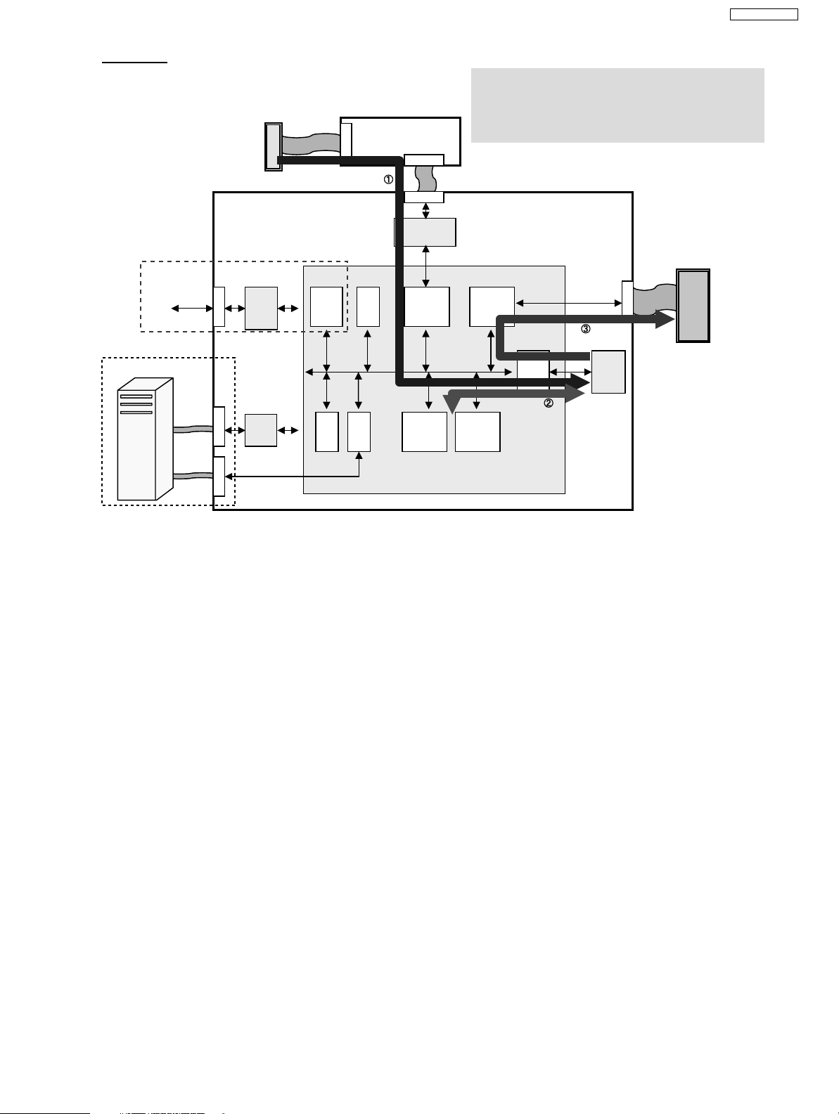
UF-5500 / 4500
[Copy]
CN59
CN510
CN61/71
CN500
SDRAM
MODEM
Scanner
I/F
Print I/F
AFE
IC503
IC400
IC300
Main Board
CN300
SDRAM
I/F
CN750
LAN
USB
USB
I/F
CPU
DAA
IC100
IC101
PHY
LAN
I/F
DSPJBIG
CN100
IC750
1. An analog image data is output from CISunit to IC503.
IC503 decodes Analog to Digital data, and outputs to IC300.
Scanner I/F in IC300 processes image data and stores it in IC400
through SDRAM I/F.
2. If necessary, the data is compressed via JBIG.
3. Print I/F retrieves the data from IC400 and outputs it to LSU.
CISunit
LSU
TEL
LINE
PC
CIS Relay Board
UF-5500 ONLY
27
UF-5500 / 4500
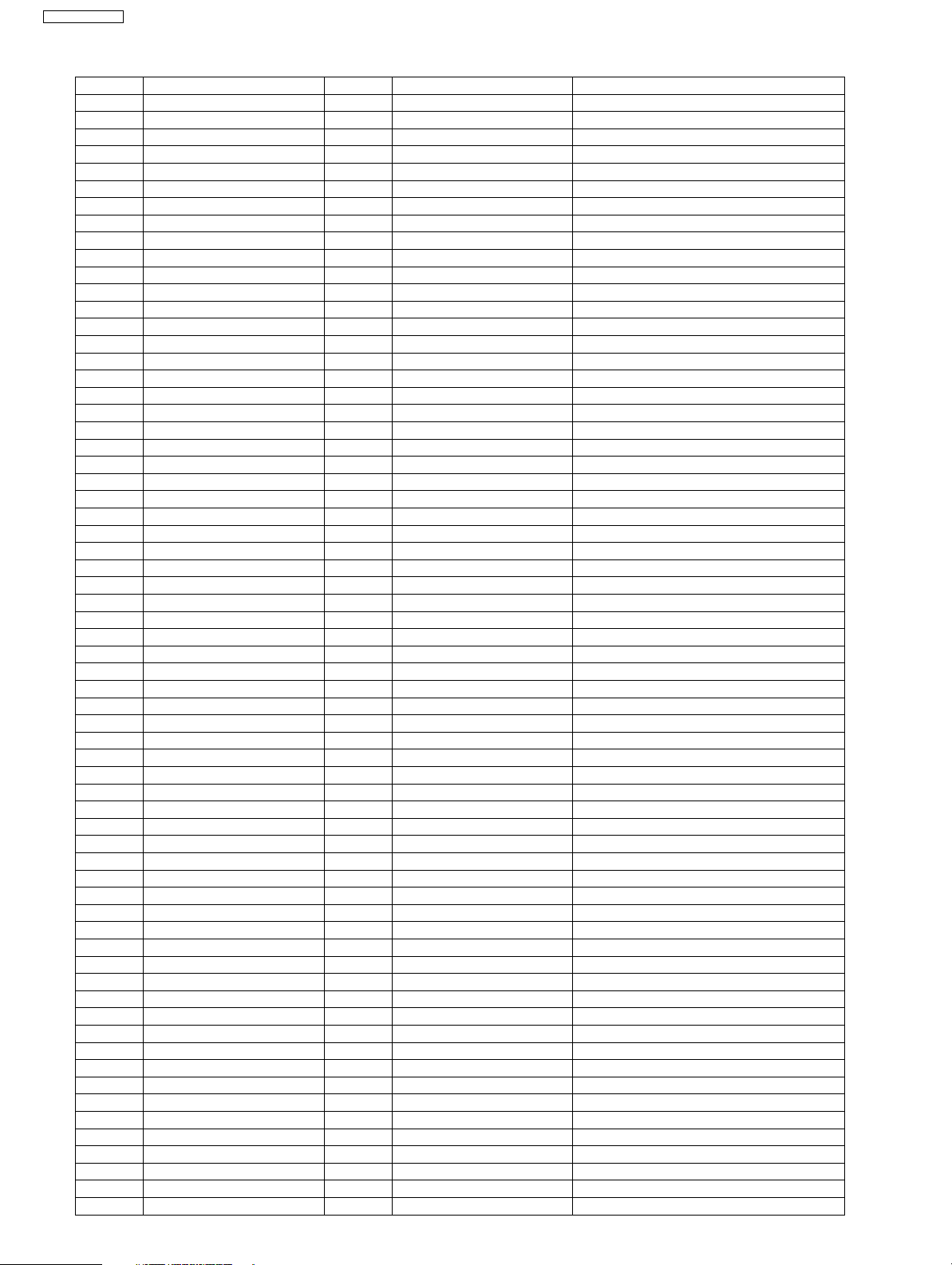
Description of Pin Distribution (IC300) SOC (System On Chip)
PIN NO. PinName I/O POWER SUPPLY VOLTAGE EXPLANATION
A02 LEDONB O 3.3V SCANNER INTERFACE
A03 NCCDON O 3.3V SCANNER INTERFACE
A04 AFEMCLK O 3.3V SCANNER INTERFACE
A05 NCCDCP O 3.3V NOT USED
A06 CCDCLK O 3.3V NOT USED
A07 PIO29 O 3.3V OPERATION PANEL INTERFACE
A08 PIO57 O 3.3V CARRIAGE MOTOR INTERFACE
A09 PIO53 O 3.3V CARRIAGE/ADF MOTOR INTERFACE
A10 PIO50 O 3.3V CARRIAGE/ADF MOTOR INTERFACE
A11 PIO46 O 3.3V FAN1 CONTROL
A12 PIO42 O 3.3V DC MOTOR INTERFACE
A13 NFRCE O 3.3V FLASH MEMORY CHIP SELECT
A14 FRMD0 I/O 3.3V FLASH MEMORY DATA BUS 0
A15 FRMD3 I/O 3.3V FLASH MEMORY DATA BUS 3
A16 FRMD7 I/O 3.3V FLASH MEMORY DATA BUS 7
A17 FRMA3 O 3.3V FLASH MEMORY ADDRESS BUS 3
A18 FRMA6 O 3.3V FLASH MEMORY ADDRESS BUS 6
A19 FRMA10 O 3.3V FLASH MEMORY ADDRESS BUS 10
A20 THRMAVDD - 3.3V POWER SUPPLY
A21 FRMA11 O 3.3V FLASH MEMORY ADDRESS BUS 11
A22 FRMA15 O 3.3V FLASH MEMORY ADDRESS BUS 15
A23 FRMA17 O 3.3V FLASH MEMORY ADDRESS BUS 17
A24 FRMA20 O 3.3V FLASH MEMORY ADDRESS BUS 20
A25 FRMA22 O 3.3V FLASH MEMORY ADDRESS BUS 22
AA01 SDMD8 I/O 3.3V SDRAM DATA BUS 8
AA02 SDMD9 I/O 3.3V SDRAM DATA BUS 9
AA03 SDMA7 O 3.3V SDRAM ADDRESS BUS 7
AA04 SDMA6 O 3.3V SDRAM ADDRESS BUS 6
AA23 VDD1.2 - 1.2V POWER SUPPLY
AA24 AFERST O 3.3V NCU INTERFACE
AA25 RING I 3.3V NCU INTERFACE
AA26 EXTINT I 3.3V NCU INTERFACE
AB01 SDMD10 I/O 3.3V SDRAM DATA BUS 10
AB02 SDMD11 I/O 3.3V SDRAM DATA BUS 11
AB03 SDMA5 O 3.3V SDRAM ADDRESS BUS 5
AB04 VDD1.2 - 1.2V POWER SUPPLY
AB23 VSS - GND GND
AB24 BTXD O 3.3V NCU INTERFACE
AB25 BRXD I 3.3V NCU INTERFACE
AB26 AFECLK O 3.3V NCU INTERFACE
AC01 SDMD12 I/O 3.3V SDRAM DATA BUS 12
AC02 SDMD13 I/O 3.3V SDRAM DATA BUS 13
AC03 SDMA4 O 3.3V SDRAM ADDRESS BUS 4
AC04 VSS - GND GND
AC05 VSS - GND GND
AC06 VDD1.2 - 1.2V POWER SUPPLY
AC07 TXD0 O 3.3V ETHERNET INTERFACE
AC08 TX_ER O 3.3V ETHERNET INTERFACE
AC09 RXD1 I 3.3V ETHERNET INTERFACE
AC10 VDD3.3 - 3.3V POWER SUPPLY
AC11 TEST I 3.3V NOT USED
AC12 USBREXT I 3.3V USB INTERFACE
AC13 VDD1.2 - 1.2V POWER SUPPLY
AC14 VDD3.3 - 3.3V POWER SUPPLY
AC15 USBXIN I 3.3V CRYSTAL(12MHz) INPUT
AC16 LSI_SCAN_ENABLE I 3.3V NOT USED
AC17 VDD1.2 - 1.2V POWER SUPPLY
AC18 NWDTRST O 3.3V WATCH DOG TIMER RESET OUTPUT
AC19 LSI_TN I 3.3V NOT USED
AC20 PSCIO2 I 3.3V INPUT PORT (FANDET1)
AC21 PSCIO6 O 3.3V NOT USED
AC22 VDD1.2 - 1.2V POWER SUPPLY
AC23 VSS - GND GND
AC24 ATXD O 3.3V NCU INTERFACE
AC25 BBITCLK I/O 3.3V NCU INTERFACE
28
UF-5500 / 4500
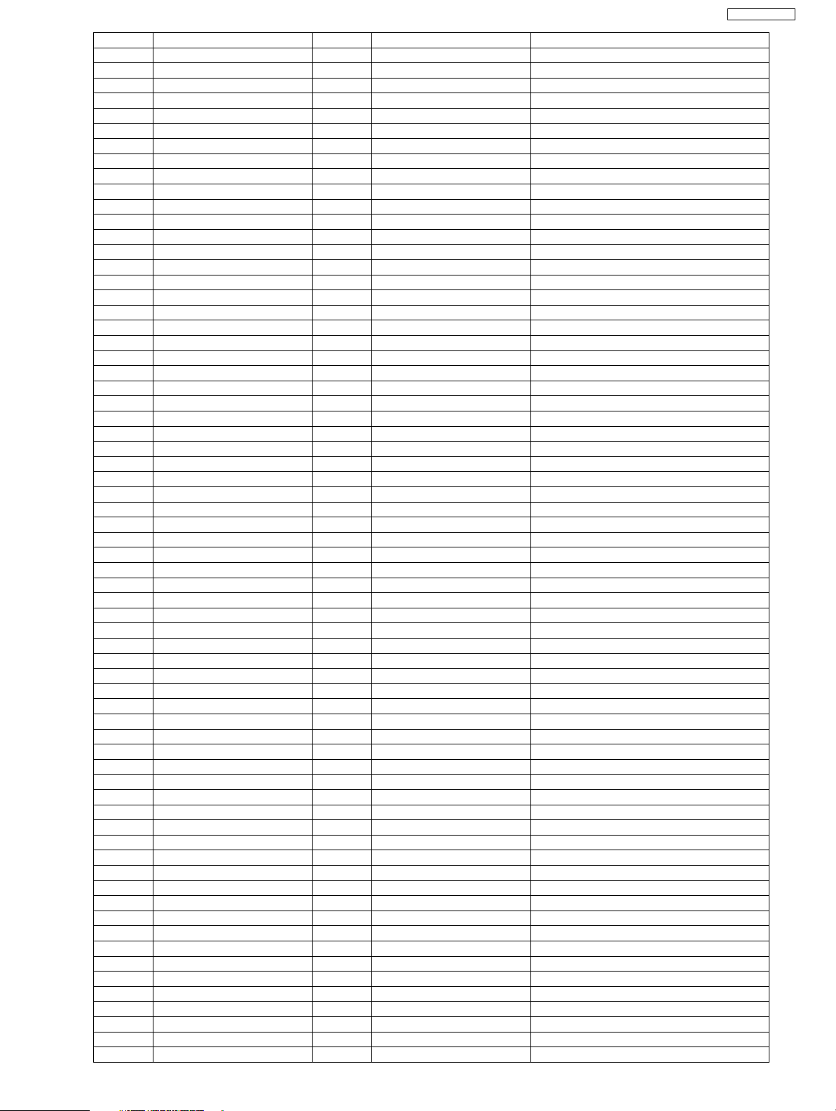
PIN NO. PinName I/O POWER SUPPLY VOLTAGE EXPLANATION
AC26 BSPCLK I/O 3.3V NCU INTERFACE
AD01 SDMD14 I/O 3.3V SDRAM DATA BUS 14
AD02 SDMD15 I/O 3.3V SDRAM DATA BUS 15
AD03 VSS - GND GND
AD04 NBATRST I 3.3V BATTERY RESET INPUT
AD05 VDD2RTC - 1.2V POWER SUPPLY
AD06 CRS I 3.3V ETHERNET INTERFACE
AD07 TXD1 O 3.3V ETHERNET INTERFACE
AD08 RX_DV I 3.3V ETHERNET INTERFACE
AD09 RXD2 I 3.3V ETHERNET INTERFACE
AD10 RX_ER I 3.3V ETHERNET INTERFACE
AD11 CLKSEL I 3.3V NOT USED
AD12 USBVSSA33_BIAS - GND GND
AD13 USBVSSA33 - GND GND
AD14 USBVDDA12_SQ - 1.2V POWER SUPPLY
AD15 USBVSSA12 - GND GND
AD16 LSI_TRSTN I 3.3V NOT USED
AD17 LSI_TDO O 3.3V NOT USED
AD18 NRST I 3.3V SYSTEM RESET INPUT
AD19 HTRCTL O 3.3V HEATER CONTROL
AD20 PSCIO3 I 3.3V INPUT PORT (POUT)
AD21 PSCIO7 O 3.3V NOT USED
AD22 PSCIO15 I 3.3V INPUT PORT (RPS)
AD23 NC - - NOT USED
AD24 VSS - GND GND
AD25 ASPCLK I/O 3.3V NCU INTERFACE
AD26 ARXD I 3.3V NCU INTERFACE
AE01 SDLDM1 O 3.3V SDRAM DQML1
AE02 VSS - GND GND
AE03 SYSPLLVSS1 - GND GND
AE04 RTCCLKOUT O 3.3V CRYSTAL(32.768KHz) OUTPUT
AE05 RTCPWRDWN I 3.3V RTC POWER DOWN
AE06 TX_CLKI I 3.3V ETHERNET INTERFACE
AE07 TXD2 O 3.3V ETHERNET INTERFACE
AE08 RX_CLKI I 3.3V ETHERNET INTERFACE
AE09 RXD3 I 3.3V ETHERNET INTERFACE
AE10 MDC O 3.3V ETHERNET INTERFACE
AE11 NC - - NOT USED
AE12 USBID O 3.3V NOT USED
AE13 USBDM I/O 3.3V USB INTERFACE
AE14 USBVSSA12_SQ - GND GND
AE15 USBVDDA12PLL - 1.2V POWER SUPPLY
AE16 USBVDDA12 - 1.2V POWER SUPPLY
AE17 LSI_TDI I 3.3V NOT USED
AE18 LSI_PROCMON O 3.3V NOT USED
AE19 LSI_IDDT I 3.3V NOT USED
AE20 PSCIO1 I 3.3V INPUT PORT (PICK)
AE21 PSCIO5 O 3.3V NOT USED
AE22 PSCIO13 I 3.3V INPUT PORT (TNR)
AE23 MDMCLKOUT O 3.3V CRYSTAL(24.576MHz) OUTPUT
AE24 MDMPLLVDD - 3.3V POWER SUPPLY
AE25 VSS - GND GND
AE26 ABITCLK I/O 3.3V NCU INTERFACE
AF02 SYSPLLVDD1 - 3.3V POWER SUPPLY
AF03 VDD3.3OSC - 3.3V POWER SUPPLY
AF04 RTCCLKIN I 3.3V CRYSTAL(32.768KHz) INPUT
AF05 COL I 3.3V ETHERNET INTERFACE
AF06 TX_EN O 3.3V ETHERNET INTERFACE
AF07 TXD3 O 3.3V ETHERNET INTERFACE
AF08 RXD0 I 3.3V ETHERNET INTERFACE
AF09 MDIO I/O 3.3V ETHERNET INTERFACE
AF10 MGTINT I 3.3V ETHERNET INTERFACE
AF11 USBVBUS O 3.3V USB INTERFACE
AF12 USBVDDA33_BIAS - 3.3V POWER SUPPLY
AF13 USBDP I/O 3.3V USB INTERFACE
AF14 USBVDDA33 - 3.3V POWER SUPPLY
AF15 USBVSSA12PLL - GND GND
29

UF-5500 / 4500
PIN NO. PinName I/O POWER SUPPLY VOLTAGE EXPLANATION
AF16 USBXOUT I 3.3V CRYSTAL(12MHz) OUTPUT
AF17 LSI_TMS I 3.3V NOT USED
AF18 LSI_TCK I 3.3V NOT USED
AF19 LSI_CW_TAP I 3.3V NOT USED
AF20 PSCIO0 I 3.3V INPUT PORT (REGIST)
AF21 PSCIO4 O 3.3V NOT USED
AF22 PSCIO12 I 3.3V INPUT PORT (POUT)
AF23 PSCIO14 I 3.3V INPUT PORT (DOCU)
AF24 MDMCLKIN I 3.3V CRYSTAL(24.576MHz) INPUT
AF25 MDMPLLVSS - GND GND
B01 AFEADC0 I 3.3V NOT USED
B02 VSS - GND GND
B03 LEDONG O 3.3V SCANNER INTERFACE
B04 AFERSMP O 3.3V NOT USED
B05 AFEVSMP O 3.3V SCANNER INTERFACE
B06 NCCDRS O 3.3V SCANNER INTERFACE
B07 PIO30 I/O 3.3V OPERATION PANEL INTERFACE
B08 MMPWR O 3.3V NOT USED
B09 PIO54 O 3.3V CARRIAGE/ADF MOTOR INTERFACE
B10 PIO51 O 3.3V CARRIAGE/ADF MOTOR INTERFACE
B11 PIO47 O 3.3V NOT USED
B12 PIO43 O 3.3V DC MOTOR INTERFACE
B13 NFROE O 3.3V FLASH MEMORY CHIP OUTPUT ENABLE
B14 FRMD1 I/O 3.3V FLASH MEMORY DATA BUS 1
B15 FRMD4 I/O 3.3V FLASH MEMORY DATA BUS 4
B16 FRMA0 O 3.3V FLASH MEMORY ADDRESS BUS 0
B17 FRMA4 O 3.3V FLASH MEMORY ADDRESS BUS 4
B18 FRMA7 O 3.3V FLASH MEMORY ADDRESS BUS 7
B19 THRMAVSS - GND GND
B20 TONE O 3.3V ANALOG(TONE) OUTPUT
B21 FRMA12 O 3.3V FLASH MEMORY ADDRESS BUS 12
B22 FRMA16 O 3.3V FLASH MEMORY ADDRESS BUS 16
B23 FRMA19 O 3.3V FLASH MEMORY ADDRESS BUS 19
B24 FRMA21 O 3.3V FLASH MEMORY ADDRESS BUS 21
B25 VSS - GND GND
B26 DOTPLLVSS - GND GND
C01 AFEADC3 I 3.3V NOT USED
C02 AFEADC1 I 3.3V NOT USED
C03 VSS - GND GND
C04 LEDONR O 3.3V SCANNER INTERFACE
C05 OEB O 3.3V NOT USED
C06 CCDSH O 3.3V SCANNER INTERFACE
C07 PIO31 O 3.3V OPERATION PANEL INTERFACE
C08 OPMPWR O 3.3V NOT USED
C09 PIO55 O 3.3V CARRIAGE/ADF MOTOR INTERFACE
C10 PIO52 O 3.3V CARRIAGE/ADF MOTOR INTERFACE
C11 PIO49 O 3.3V OUTPUT PORT(HSSPMUTE)
C12 PIO45 O 3.3V DC MOTOR INTERFACE
C13 NFRWE O 3.3V FLASH MEMORY CHIP WRITE ENABLE
C14 FRMD2 I/O 3.3V FLASH MEMORY DATA BUS 2
C15 FRMD6 I/O 3.3V FLASH MEMORY DATA BUS 6
C16 FRMA2 O 3.3V FLASH MEMORY ADDRESS BUS 2
C17 FRMA5 O 3.3V FLASH MEMORY ADDRESS BUS 5
C18 FRMA9 O 3.3V FLASH MEMORY ADDRESS BUS 9
C19 THRMSTR0 I 3.3V ANALOG INPUT(THERMISTOR)
C20 TONEAVDD - 3.3V POWER SUPPLY
C21 FRMA14 O 3.3V FLASH MEMORY ADDRESS BUS 14
C22 FRMA18 O 3.3V FLASH MEMORY ADDRESS BUS 18
C23 FRMA23 O 3.3V FLASH MEMORY ADDRESS BUS 23
C24 VSS - GND GND
C25 DOTPLLVDD - 3.3V POWER SUPPLY
C26 DOTCLKIN I 3.3V CRYSTAL(20MHz) INPUT
D01 AFEADC5 I 3.3V SCANNER INTERFACE
D02 AFEADC4 I 3.3V SCANNER INTERFACE
D03 AFEADC2 I 3.3V NOT USED
D04 VSS - GND GND
D05 VSS - GND GND
30
 Loading...