

Panasonic rm 610, rm e610 schematic
ORDER
NO.
RD7912-TI022
Panasonic
Service
C
II
IC
K
PI
r
Hand
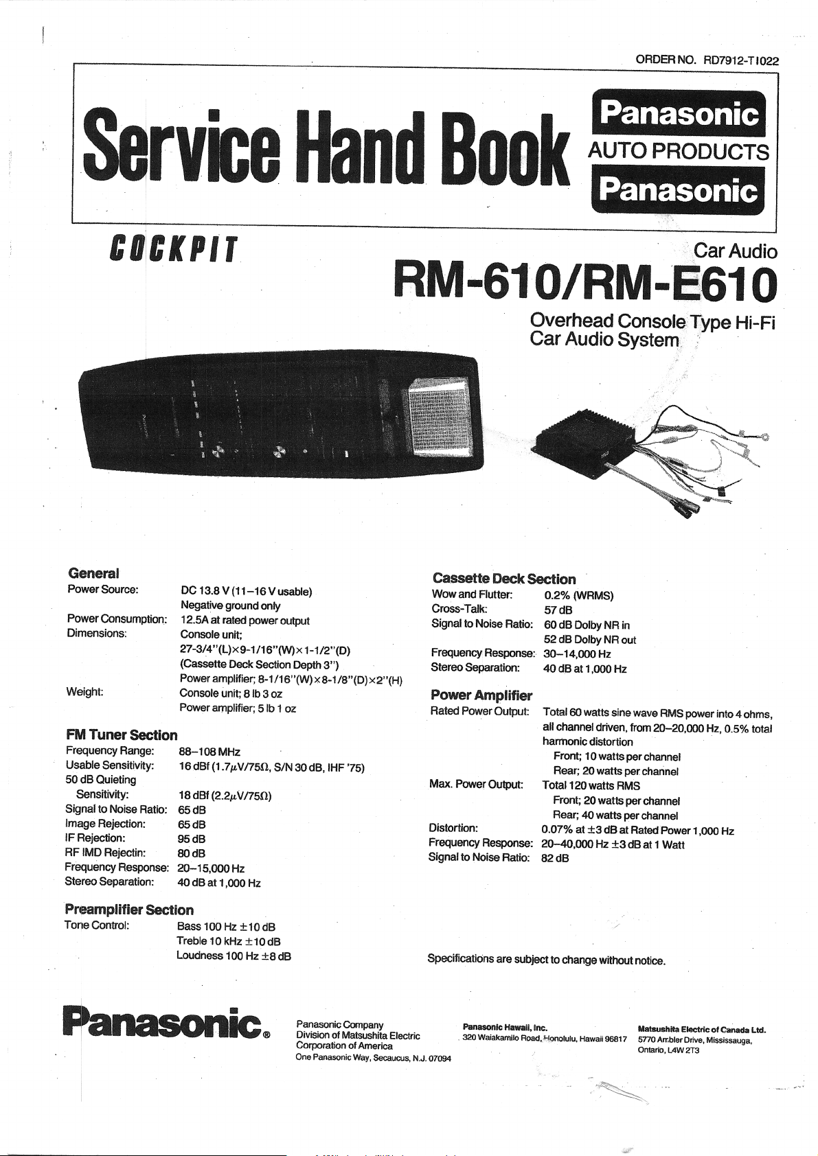
RM-610/RM-·8610
Book
AUTO
PRODUCTS
Panasonic
.·::
·:
Overhead
Car
Audio
Console
Systefl1
;
. ·
··
car
Type
Audio
Hi-Fi
General
Power Source:
Power Consumption:
Dimensions:
Weight:
FM
Tuner
Section
Frequency Range:
Usable Sensitivity:
50
dB Quieting
Sensitivity:
Signal
to
Noise Ratio:
Image Rejection:
IF
Rejection:
RF
IMD
Rejectin:
Frequency Response:
Stereo Separation:
Preamplifier
Tone Control: Bass
DC
Negative ground only
12.5A at rated power output
Console unit;
27-3/4"(L)X9-1/16"(W)x
(Cassette Deck Section Depth
Power amplifier;
Console unit; 8 lb
Power amplifier;
88-108MHz
16
18 dBf
65dB
65dB
95dB
80dB
20-15,000Hz
40
dB at
Section
Treble
Loudness
13.8 V
(11-16
V usable)
1-1/2''(D)
30
dB,
3")
IHF
8-1/16"(W)x8-1
3
oz
51b
1 oz
dBf(1.7~.~-Vn5!l,
(2.2~.~-Vnsn)
1
,000
100Hz
10kHz
100Hz
Hz
±10
±10dB
dB
±8
S/N
dB
/8"(D)x2"(H)
'75)
Cassette
Wow
Cross-Talk:
Signal to Noise Ratio:
Frequency Response:
Stereo Separation:
Power
Rated Power Output:
Max. Power Output:
Distortion:
Frequency Response:
Signal
Specifications are subject to change without notice.
Deck
and Rutter:
Amplifier
to
Noise Ratio:
Section
0.2%(WRMS)
57
dB
60
dB
Dolby NR
52
dB
Dolby NR out
30-14,000
40
Total
all channel driven, from
hannonic
Front;
Rear; 20
Total120watts
Front; 20
Rear;
0.07%
20-40,000
82dB
dB
at 1
,000
SO
watts sine wave
distortion
10 watts
watts per channel
watts per channel
40
watts per channel
at
±3
Hz
Hz
dB
in
Hz
20-20,000
per
channel
RMS
at Rated Power 1
±3
dB at 1 Watt
/
RMS
power into 4 ohms,
Hz,
,000
0.5%
Hz
total
~nasonic®
Panasonic Company
Division
of Matsushita Electric .
Corporation of America
One
Panasonic
Way,
Secaucus,
N.J.
07094
Panasonle
320
Waiakamilo
Hawaii,
Road
Inc.
..
J;i
onolulu, Hawaii
96817
-
.
·~
Matsushlta Electric
sno
Arr.bler
Ontario,
Drive, Mississauga,
L4W
2T3
of
Canada
Ltd.
Contents
L
Introduction . .
2.
Block
Diagram . .
Circuit
3. Tuning
4. Tuning Diallndicator
5.
Mixer
Circuit
6.
AGC Circuit
7. FM Detector
8. MPX
9.
1
11
Circuit
INQCircuit .
0.
Muting and Noise Reduction
. Level Meter .
...
Descriptions
Circuit
....
....
.
..
.
....
..
...
..
.........
..
.
..
..
...
.......
..
. ..
. ... . ..
.
..
..
. . . . .
.
...
...
...
. .
.
..
....
......
..
. .
.
..
..
.......
. .
..
..
..
.
...
.......
. .
...
. ...
.......
.
....
...
..
...
.
..
....
........
.
....
Circuit
.
.
...
. . .
..
....
...
........
..
.......
...
.....
....
..
. . .
......
..•
...
. .
.....
..
.
..
. ..
....
.
..
2-4
.
...
.
...
. .. . .. .
5-6
..
. . .
..
.
....
7
...
...
.
....
8
......
.. .
....
8
-
~
.
.•..
......
9-11
..••
......
11-13
...
..
..
..
...
14-18
..
...
.
.......
19-20
...
....
..
....
20
1. Introduction
Is it
possible to introduce high
that is subject to road noise, ignition noise and other types
interference, as well
results? Fortunately, the answer is yes, but it ins't simple. To enjoy
high fidelity audio in a moving vehicle, certain special performance
and functional criteria must be met; special
and improve reception under adverse conditions , as
construction to resist vibration and the thumps and bumps of the road.
The research and development of a product to meet these
requirements gave birth to the RM-610. The
achieving excellent high fidelity performance, while the car is standing
still,
or on the move, and
fidelity
sound into a moving automobile,
as varying FM signal conditions, with
ci
rcuits to reduce noise
well
as rugged
RM-610
is capable of
in
both weak and strong
FM
signal areas.
of
good
12. Loudness
13. Dolby NR System
14. Automatic Reverse
15. Automatic Eject Control . . .
16. Sound Equalizer Model RM-E61
17.
DC-DC
18.
BTL
19. Protection
20.
Power
21. Dome Lamp . .
22. Basic Logic
23. Trouble Shooting Guide . . . . . . . . . . . . . . . . . . . . . . . . .
24. Schematic Diagram
The RM-61 0
components. The cassette deck features a Dolby Noise Reduction
(NR) system. A high-power main amplifier provides audio power to
spare, and at very respectably
optional equipment in the
adjust the frequency response of the system,
dif
ferences in personal
different accoustical environments. For maximum
are not included in the RM-610. There is
quality speakers for car use; that come
sizes, and in different types of enclosures. Thus it is possible to
optimumly select speakers that are most likely to fit
please the listener.
Control Circuit
....
Control
Converter .
Circuit
Circuit .
Supply Control Circuit
is made up ·
..
..
....... .......
..
........
Circuit ·
.....
RM-610.
listening
.
.....
..
of
low
..
...
........
........
...
. . . .
.. ..
......
.
....
.. ..
....
..
. .
...
. . .
.
..
. ..
....
. .
......
a number of discrete Hi-Fi type
distortion. The graphic equalizer is
The equalizer makes
habits, and for variations found
.
.....
.
..
.....
..
..
....
...
....
.
....
..
...
.....
. . .
...
.
.. ..
.. .. ..
. . . .
..
..
0
.
...
.
........
. .
...
.
..
.
....
.....
...............
. . . . . . . . . . . ,
.....
.
...
.
...
......
.
....
a wide selection of good
in
a variety of shapes
...
..
..
.
..
.
.......
..
.....
.....
.
..
.
....
..
.
.. ..
it
to
make up for
flexibility,
in
the car, and
.. ..
.. ..
.
..
. . .
possible to
speakers
..
23-25
.
..
26-27
...
. . 29
. . .
29-30
30-31
32-35
36-44
and
.
21
22
25
28
.
28
29
in
-1-

2. Block Diagram
-
---
--
--------~
CASSETIE
4::€~
R-CHJ::€..1~
TAPE
DECK
.{~·
Jlo(oi-"
HEAD
•
4Cl:~
~(}:_9
PROORAM
lNXCATOR
:
:
L
Ayr_o
https://manualmachine.com/;
: (@:
:
(@
: '
:~R
L-cH
~
~
L·C4
I [
4)(3)@!1
_R§~E~s~
_s~
~------
L
I'
tam
I R.CH+a
JR-CH
l
_4m
1
@!1~!
.J.-JL
"'
'
I'
!:
~",
Notes:
Tape
FM
signal
Power
Power
•I
,,
:1:
11
, , ,
;t;',','',','i
signal line ... .
line ......... .. ....
Supply line
supply line
I
~
~,
','!~',',','
..................
...........................
when tuner used ...
.
..
....
.................
TUNER
ANT
L-CH
~:
~
.
5
.
~
~
!
.-----==-
r.,.
r
...
,
T""'r
J
~
~.·
"-',','~,
,',
,',,',',','!,',',','"'',',"Y:-,',',~'.',',',~,',',',','~','t?~~im:~~:tt~}:s~:(@:~rl~:~~~~;~;~;~;~;~;~;nx~:~:~;~~;~;;;x
~
-
•
...
---.
~
_.,.
~
---------------------------:
:
'
~
.
.
•
...,
.....
_,
!
:
~neiGray
~
~~~.J
Brown
3.Vacant
6.Red
7.YoUow
R·CH
R.CH
L-CH
rrlt.-CH
f!Urtl<>
:~
''
h
t:::
r::
:1:
!
:
::
,jBI~~c:k!
1
~~te!Blue
av"""
.....
.Y.tlow
7
MUT
I
ING'
'
'
'
:·
..
....
L-CH
R.CH
....
MUT
I
NG
PREAMPLIFIER
L·
CH
..
CH
.....
---
l
J
~·-I
line
-
"L.CH
I
FRONT
'~"
* •
L-CU
REAR
..
~H
0
.,
..
FRONT
-----·----
-=-~-~-~
------------------
-
---
.. ·) •
.
--
-f~-~~
----
'I
...............
~;-~-~;
-;-~
-
...
-
- -
--
•
W O
(
21
(3)
0
B
---
If</
.
§
2SC1327
2SCI327
•
.._
....................
----.;;.
~---
Power
line
'""
L---.J[Zl8Tl
1
r
•
'""
,....
.:..·
-----
eau
-;-~-~-~~-;;-~;-;-;-f;_;_;_;_;~;-~-;-;-;
--
to
mel"'·
L...r.
-
.....
------
•·
1
• I
~
M~!
p
.......
_
...
._
...
POWER
AMP
RVIM51S7L
Bll
POWER
AMP
''"""'
,f;--1
.1:
''
'I'
I
J
I IJI
*
_--
--
--
t-----
I
11-------
R.CH
®~,
[X]
TAPE
L...,
I '
11
,,
·~
'
E;;;;
1:
____
-
..
-
...
--
-------:-.:------
~
;
--
w .
_
.
0
•
"
....------.
~
!"'~
~,
-2-
Shl
..
~
..
-
....
'
t't."-tb\0
d
Black I
~A:11~
..
=-=--
-
..
-=-=
....
Gray
(Fronl)
--
Shield
--
..
-
......
0~
.J
--
c...c~~
~-
Fig.1
-3-
f\-\u.Ui
~'
t;cJA.._
O\C.rv~
1:

--
--
t
[I]
L.CH
~'
''
·
~
.,
' '
t
-
----
3]i
2. Block
- - - -
PR
EAMPLIFIER
;.,-,..-
•·
CH
-
'"""
R.CH
__...
~t:.
MUTING
(O
Diagram
-.,_-..~
7
APE
.....
FRONT
.
eau
'"
0
®
®_ill_
®
®
-£
'
'""'
J
•rTAPE~
1 1
11
~~
:..--
,,
(i
[X]
,
11
11
..
,,
'
'
:::::::E:
R-CH
MUTING
,
-
-
(OP
TI
ONA
L)
k.cH
(j)aAV
R.cH
IN
DI
CATOR
OFF
i}
.'
1i
OF
'
i
p..
rR-CH
f
1
11
1 1
''
~
L.cHp...
I
::
11
11
'
11
f-
FM
1
§
· ·
r·~-l
ffi
- - -
lA)H
-----,----,
..
,.,
e~N!R!'I;.
250Hz
~~!R_DI:.
~R.?:_
""'
3.5kHz
~~RpL
_
10kHt
~~~---
',
--
'~
j,',
,-
t,','
;
',;,~=~x~'X':~,'
~----11
~
:
~~}Gray
8
!
~
}
Biack
Gre
~~e:lt,}erown
Y
~~.';,'"}Blue
!
:~ttelm.c~~
:
~~~.Jalue:
:l.Vacant
I
.....
'
7,Vellow
1
f
·~'
•
Shlllld
j
'
'
'
JcFronll
'
-----------~
,
;f,};,;:~
'
;f,X,
,~:
...
I
(.01:
R.CH
I
,®
1°
®
®~
(0[--...
.®
~
'
,',:,X~f':';';'~'J;';';'
r-
----:-
·;=
·
=·=:
=-
-
·-:-
=·=
;;:
,
';
'
;';';
'
~'Y:::~
S
__....
-
-:
:
:;:
b
;~':'Xi,{[;l;,;x,::X
igna,
"""
-
-;::c;;
FRONT
L.CH
?~:~:?:=Y'X;If'X':i
ran
~
-
A~
2SCI327
INV
.
AMP
2
SCI327
I
r-
I
f
~
POWER
~
-
~AM~P~~
RVIM5157l
BTL
POW
J
·
···~~MiPSlJ
RVIM5157L
....
f
"'
,
'J
'N,'~'
,',y
,
','
',';,,,-JU
f
J-~
----
.
ER
I
~~~-
--~------
--------------
--------~r-~
------1,___
-
-----------------
-- ·;e
-
"'
G."'
EY
RI
;o
GR
~
UE
.
,_
"'
!!
!!
REO
+
R-CH)
FUSE
-
ISA
~
------
~
-----
~
/~
Ag.1
-3
SE
,
'
-
-
•-
~S~
~~
')'\-~

--------------------------------------------------------------------------------------------------------------------------------------------------------------------------------------·---,
3.
Tuning Circuit
The
FM
tuner
employing
diodes).
manually
radio
Tuning
varactors
varactors
output
vottaga
(VR1
a
and
along
the
Here's
(A) Pres$S3
time,
'preset
VR1
greater
voltage
applied
There
turned
tuners.
is
accomplished
D3
capacitance
circuits,
across
01
toVR1
when
01
operate
wtth
there
stations.
how
Input
3
current
LED
lights
the
base
base
of
the
applied
up
of0101,
applied
varactors
to
their
H
worl<s:
IS
grounded
to
of
0101
the
to
Is
to
takes
are
no
to
tune
D6.
local
these
04)
.
These
related
the
related
Tuning
flow
up,
and
0101
depands
vottage
vottage
R142,
the
varactors
applied
the
varactors.
advantage
(voltaga
variable
In
a
electronically
Saa
Fig.
and
oscillator
varactors
reslstros
switches
manual
variable
through
through
the
through
to
developed
R143
to
the
capacitors
radio
station,
2.
As
tunes
(02),
tuning
resistors
Is
as
simple
R1
LED
voltage
0103.
upon
the
base,
andR144,
. .
The
base
of
an
electronic
controlled
variable
or
variable
as
there
are
by
changing
the
VQ)tage
the
is
0111
changes,
RF
amplifier's
and
mixer
cont
_
rolled
by
era
switched
(51
04,
drop
the
across
oonverse
of
into
to
S4)
are
pressed.
function,
and
VR102
as
turning
output
3
goes
and
VR103.
across
VR1031s
The
a.
mount
setting
of
VR103.
the
more
0101
the
voltage
andthegreaterthevottage
Is
also
0101
,
a
lower
Circuit Description
1t
is
preset
is
tuning
system
capac~ance
lnductors
to
be
in
conventional
the
voltage
across
so
does
the
(01)
Input
to
the
clrcutt
VR104
volume
low
See
vottage
conducts
divider
true,
voltage
010).
resistors
SwOOh
52
operate
control.
and
Flg.2.
applied
The
ff
a
and
The
one
to
allows
The
on
the
higher
,
the
made
lower
will
be
51
S4
to
at
(07
variable
swttchas
to
a
of
·
set
select
tuning.
Preset
Preset
station
necessary
lime
This
R128,
same
B+level,
function
Tuning
SwHch
Pushed
possible
posltions
tO
a
station
any
one
tuning
your
will
then
to
the
power
Is
done
when
worl<
it
when
circuit
Position
51
(Manual)
52
(Preset!)
S3
(Preset2)
S4
(Preset3)
to
tune
the
,
as
well
,
as
well
of
4
stations
selector
most
popular
be
heard
instruct
IC101
has
been
automatically,
the
power
as
pressing
is
effectively
pressed,
functions
IC101
(Low)
entire
as
the
as
at
1 priority
sl<!tlon
first
·
shuf
as
is
_
first
52
manually.
out
at
any
Terminal
<l>
@
@
®
manual
the
the
(52)
when
to
turn
off.
follows:
turned
of
time
FM
broadcast
preset
push
on
the
on
the
circuit,
.
position
positions
of
a
button,
Preset
power
one
current
on
and
When
LED
Illuminated
D109
D110
D111
0112
Tuning
switch
of
the
flows
it
C104
and
.
band
on
lf
the
manual
,
then
lt
without
Selector
Is
stations
through
essentially
charges
allows
any
is
possil51e
any
turned
after
51
VAin
control
of
position
further
1.
on.
C104
does
up
to
to
54
VR101
VR102
VR103
VR104
the
This
1t
each
and
the
the
Tun
ing
Control
Voltage
to
Var
ac
to
rs
3
to
Is
:;
;;:
to
IC101
I
re
;;:
A102
._-+l'""::'±==r-=ci-,
I
..
,u,~
I I '
1;)
•
0
N
"
s
j
"
!
~
0 0
6
~
~
~
N
&.
.5
a:
a
i5
0.
,
-
..
s
0
z
~
0
"
..
"
I I
'--+------o
H
>
,I
"
•
8
~
G
·H
~
g
·&
c
~
i
~
I
t-----------__,J>--------------()
18.5
See
.tuner
schematic
varactors
for
location
of
+8
V)
+
8
IS
V)
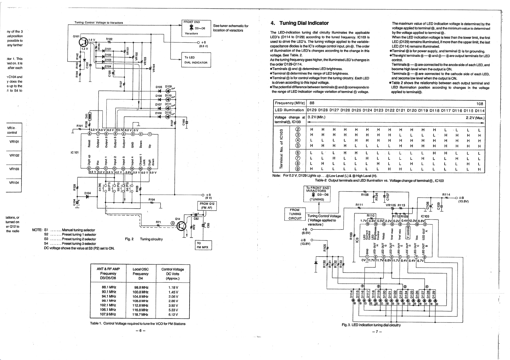
4.
The
LED's
used
capacitance
of
illumination
voltage.
As
the
the
order
•Terminals
•Terminal@
•Terminal
is
driven
•Thepotenlialtf
the
Frequency
-----
LED lllumlr.
-------
Voltaga
terminal@
Note:
Tunin1
LED-indica
(D114
to
drive
See
tuning
D129-t
@ar
®is
eooon
ranga
of
0
"'
§
0
0
z
...
.5
E
~
Foro.;
to
Ill<
diO<
of
Tat
fret
de
LE
cha
,!
1-
1
"
.
1
.·
'
{
(B)
PressS2
·
Input
21s
3
Is
returned
pressed,
determines
voltage
other
selector
grounded
to
except
how
to
QO
high.
that
much
to
the
switches
through
The
same
now
0101
varactors.
are
R104,
LED
will
And
pressed
output
action
D110
oonduct
so
.
2
goes
occurs
Is
and
it
goes
low
as
when
on
,
and
develop
when
and
any
53
VR102
a
oontrol
output
was
of
the
-5-
Muting
When
any
to
momentarily
and
provides
ground.
program
one
of
cut
a low
Releasing
to
be
heard.
switches
the
radio
Impedance
the
51
switch
to
S41spressed
station
audio
path
from
turns
014
signal,
the
off
to
audio
and
change
014
amplifier
allows
stations,
Is
turned
the
012 to
radio
u
[]
f
(P2)
set
ANT&RFAMP
Frequency
D3/DS/06
86.1
90.1
94.1
98
102.1
106.1
107.9MHz
Table
1.
--------,
to
ON.
MHz
MHz
MHz
.1
MHz
MHz
MHz
Control
VoHaga
u_
~1
Fig
. 2
Tuning
clrcunry
LocaiOSC
Frequency
04
98.8MHz
100.8MHz
104.8MHz
108.8MHz
112.8MHz
116.8MHz 5.33V
118
.7MHz
_
required
to
tune
the
VCO
Control
DC
(Approx
for
FM
~
Voltage
Volts
1.18V
1.45
2.06V
2.66V
3.92V
6.12V
Stations
-
.)
V
or
on
NOTE:
51
.......
Manual
tuning
S2
S3
S4
DC
.......
....
..•....
vottage
.
..
Preset
Preset
Preset
shows
tuning
tuning
tuning
the
value
selector
1
selector
2
selector
3
selector
at
S3
-6-
1:
ny
of the 3
Jalposition
possible to
any further
;tor
1.
This
1edon.
after
each
1C104and
y
does tha
~up
to
. 1 to
S4to
tatlons,
or
turned
on
erQ12to
the
radio
ltis
the.
NOTE:
S1
.......
Manual tuning selector
S2
....
...
Preset tuning
S3
.....
..
Preset
S4
.....
.. Preseltunlng3selector
DC voltage
shows
·Tuning
Control
Voltage
to
~~~~----4---+--L~~~
..-
N
...
t;
!$
Jg~~~~~~
10101
I
tuning 2
the value at
selector
selector
~
S3
(P2) set to
8
>
?"'
~
E:
I
-------
ON.
Varactors
~
~3
<")
"'
:; :;
N
M
i
l
.5
.s
Fig. 2 Tuning circuitry
I
~
0105 0109
~
'CV
0108
~
=
0107 011)-,..;
G-<
c
~8
~~
0
..J
c
'0
AI04
'M
l
-,
I 014
I
A71
\:
__
_____
I
I
@
_ _
0
+B
(8.5
To
LED
DIAL INDICATOR
0
TO
FM MPX
See tuner schematic for
location
of
V)
I
+B
(5
V)
varactors
4. Tuning
The
LED-indication tuning dial cirouUy illuminates
LED's
used
to
capacitance diodes
of
Illumination
voltage.
Aa
the tuning frequency
the
order
•Terminals@
•Terminal@
•Terminal@
Is driven
eThepotentialdiflerencebe!weenterminals@and@oorrespondsto
the range
Frequency
LED
Voltage
terminal@,
Note: For
Dial Indicator
(0114
to 0129) according to the tuned frequency.
drive
the
LEO's. The tuning
Is
the
of the LED's changes according to
See
Table.
2.
0129-D114.
according to this
illumination
0
"'
5
-
0
d
z
a;
c
·~
~
goes
and@
determines LED brightness.
determines
is for oontroi
of
LED
Indication
(MHz)
change at
!Cl
03
®
®
@
®
®
0
@
®
0.2
V,
0129
To
VARACTORS
I
FROM
TUNING
CIRC
UIT
+B
(6
.
SV)
+B
(13.8V)
vo~age
IC's voltage
the
0129
0
oontrol input,
higher,
the
illuminated
range of LED brightness.
voltage
from the tuning clrcutry: Each LED
Input
voltage.
voltage variation of
88
D128
.2V(Min.)
H
H
H H H H . H
l l
l
H H
l
L L
l
L
L H l l L L
H
l l L
Ughts
up
...
@)low
Table-2
Output
FRONT
END
'
03-06
(TUNING)
Tuning control Voltage
(Voltage applied to
varactors)
o---
Q---
~
the applicable
applied to the
0127
H
H
H
IC103
variab!&-
pin@.
The order
the
change
In
lhis
LED's changes
terminal@ voltage
D126
0125
0124
H H H
l
H H
H
L
H
H L L
L H L L L
l
L
level
(l)
&
®Hig
h
terminals and LED Illumination vs.
level
R108
R111
8
ffi~~
c;:,§
...JO(J
a:
The
maximum value
vo~age
applied to
by
the
voUage
Is
In
.
H
L
When the
LED
LED (0129) remains
LEO (0114)
•Terminal
eTheeightterminals@-@and@_:_@are
control.
Terminals@-®
beOome
Terminals~-@
and
eT
LEO illumination
applied
D123
0122
H H H
H
H
H
H
L
L H H
l
remains
@lis
high level when the output is
become
low level when the output
able
2
shows the relationship between each output terminal and
to
termlll!'i@. ·
0121
D120
H
L L
H H H H
H
L
L L H H
L H L H L
l
H
l l
~-
~~~~~~~~
~a·
l
H
(H).
1~
fil~i
..JQ)
~ ~
"'
j_
i
(,)
>
g%
§~
Vohage
lt;
I
u
VR105
~
e ;
> > >
g~
H
change
R113
"
§w
H
L
§c
of
LED indication
terminal@,
applied to terminal@.
Indication voltage
Illuminated, if more than the upper limit,
illuminated.
for power supply, and terminal
are connected to tha anode side of each LED, and
are oonnected to
position
0119 0118
H H
voltage
and the minimum
is less than the
according to changes
0117 0116 0115
is determined by
(j)
·
outputtermlnalsforlED
ON.
the
cathode side
Is
ON.
•
L
l
value
is determined
lower limij,
Is
for grounding.
·
of
each LED,
In
the voltage
2.2V(Max
l
L L H H H
H
H H H H
H H
H H
L L
l L
l l l l
L
L
of
terminal@,
IC103
L L l
+B
(13.8V)
H
!;..,
s
ffi
..J
§o
§m
108
0114
L
H
L
l
H
the
the first
the
last
.)
ANT&RFAMP
Frequency
03/05/06
66.1 MHz
90.1MHz
94.1 MHz
98.1 MHz
102.1
MHz 112.8MHz
106.1
MHz
107.9MHz
Table 1. Control
locaiOSC
Frequency
04
98.8MHz
100.8MI:fz
104.8MHz
108.8MHz
116.8MHz
118.7MHz
Voltage required to tune the
-6-
Control
VCO
for FM Stations
VoUage
OCVoUs
(Approx.)
1.
18V
1.45V
2.06V
2.86V
3.92V
5.33V
6.12V
t
~t~t~t~~~
-
Fig. 3. LED
indication
tuning dial circuitry
-7-

5.
Mixer Circuit
Double-balanced mixer is used in order
characteristics with wide dynamic range, which minimizes unnecessary
signals
in
RF
input signal (fl)
The
local oscillator signal is applied
through
The
sum
during frequency conversion.
the output side.
is applied to Terminal@
(bl),
frequency conversion takes place
and difference signals
of
to
provide
good
of
~and
to
terminal
f1
&
fL
and their harmonics appear
diodes
®
of
(bl).
at diodes
frequency
After passing
01-01o.
@
07-10
Mixer
6. ·
AGC (Automatic Gain Control) Circuit
07-010.
Local
OSC
Fig. 4 Mixer Circuit
Because balance circuits,
other than
fi-
Because the necessary
after passing through filter
Impedance
Signals
terminated by
ffi
~,
I I
:
@I
L_
Frequency higher
and
fL
fl+fl
--,-
of
R2s
50
--l
I I
:
I
and
&
n.
I
~
I I
L
fL
signals appear at terminal 6
higher than input signal
r--
I R261 I
r33
__J
I
Terminated
than "fl
(50!1)
consisting~
fl-fl
are cancelled each other and
of
IF
(T2
C33
is high to the
L---,
C32
1 :
__
_j
(bl)
output signal is only
&
C32)
, and applied to IF
IF
(fl)
and
IF Output
I
I
IF
Matching
&<Q>,
are employed, signals
as an output.
fl-fl,
signal.
local oscillator
only f1+fl
it is
take.n
Amp.
signal
(fl)
&
out
are
Transistors
strength) to switching diodes
Q6
to
09
applies a varying voltage (according to
0:.
MA
AGC
oRa
C1ID
r~
02
11
56
IDOl<
OP
and
018
in the antenna tuning circuit
oR12!DDK
signal
to
vary the
amplifier, with wide dynamic range,
Q
for a
35-40
dB range of signal strength. A buffer
couples
®
the
AGC
circuit to the
IF.
Fig. 5.
AGC
-8-
Circuit
I

AGC amplifier
figure
5.)
1 . When a strong signal is received from the antenna, it the signal is
amplified
Q7 [point@}.
2.
Because only the
rectified at
point
3.
As a
increases.
operation during high signal strength input (Refer to
by the buffer
011 and
©
reduces in proportion to the signal strength.
result,
current flow at
amplifier
amplified
012, ;md smoothed at
06,
and passed on to the base of
If
signal appearing at point@ ,
point@
becomes low, and potential
C44,
the potential at
4. When potential at point @ increases. current flow between the
collector and emitter become difficult, and consequently, potential
at point ®decreases.
5.
Because potential decreases at point ®
decreases in the same way, and switching diodes
change from ON
circuitry is thereby such that resistance is directly connected to the
is
secondary
6.
Consequently,
gain lowers.
to
OFF.·
The condition
coil,
and;as a result, the Q is damped.
the Q
of
this
resonance Circuitry
,
the voltage at point
02
and
of
the antenna tuning
decreases, and RF
®
018
7.
FM Detector Circuit
The RM-61
0
uses a quadrature detector
Basic
Operation
The quadrature detector, 3
amplifier are
quadrature phase shift circuit (essentially made up of inductance,
capacitance
The
IF
to the phase shift circuit and the quadrature detector. By the time
IF Input
all
located on a single AN377 chip
and
resistance) is
signal is fed into the 1st
to
detect the FM signal.
IF
limiter amplifiers and an AM
(IC
externally
IF
mounted.
limiter amplifier, and fed through
Phase shift circuit
fo
the signal passes through the
bottoms of the
series
of
of
the
IF
frequency, in. step with the audio signal. The quadrature phase
shift circuit follows the frequency shifts of the
1
).
The
produces a sinewave signal of the same order of frequencies,
accept that as the frequency changes the phase difference
between the
as follows.
fi
Quadrature detector
IF
signals waveform are clipped, and what was a
sinewaves now
signal varies above and below the
two
signals changes to more
3
stages of limiting the tops and
looks like
1---o-~
squarewaves. The frequency
10.7
or
less than
MHz
IF
IF
signal and
90
degrees,
output
center
-9-

Wheri the
be the
shift circuit
output signal
IF
case
signal is
if
will
10.7
no modulation is present, the signal from the phase
oo•
be
be zero.
will
phase; the average value
of
out
See
Fig.
7,
Figs.
and
8
of
show what
9
center frequency), as would
(the
MHz
the
signal is above and below the
happens when the
frequency~
negative, respectively. Relative waveforms in the quadrature
detector are
Quadrature
Phase
IF
resultant output signal becomes positive
The
follws:
as
Signal
Shift
IF
goo
center
or
(a) The IF
signal equals
phase, and the output signal
signal is less than
IF
The
(b)
phase, and the output
of
go•
MHz, the phase shift signal is
.7
10
essentially zero.
is
MHz, phase shift signal is less than
.7
10
is essentially positive.
signal
go•
out
of
IF Signal
Signal
Output
(average value=O)
Quadrature
Output
(average
Phase
IFSignal
Signal
value=+)
Shift
f2
Fig.
Signal
7
Fig. 8
l
I
I
I
\
(c) The
greater than
negative.
signal is greater than
IF
900
out
of
MHz, the phase shift signal is
io.7
phase, and the output signal
essentially
is
-10-
Quadrature
Greater than
IF Signal
Signal
Output
(average
Phase
go•
value=-)
Shift
Signal
Fig.9

The resultant output signal
by
comparing the
quadrciture
(See
provides an undistorted audio signal to the AM
8.
MPX
Mode
control
detector is
FIQ.
10)
which is impervious
Crcuit
circu
IC
1
AN377SO
IF
AMP
!!o
OET
is
IF
it
derived in the quadrature detector
signal
and the phase shift
actually
(S
a balanced differential amplifier
Fig.
tereo Auto/Mono
signal. The
to
thermal variations and
amplifier.
fo
FMinput
. signal
10. The Ouadrature detector is·a balanced differential amplifier
which detects
o---fl
o--+-oooooH
the
Switch)
,_.;;;.;..;..;;;;~_,
audio signal, without distortion.
3. When in the FM auto mode, and
Level
(0)
4. When
S.
01S
12
drops, and the FM reception signal is forced to
monaural (Refer to the operation explanation
decoder.
In
this way,
changes from Low to High level, and
switches
),
finally
making the mode become monaurai.
pushing the mode switch
06
(SS)
ON,
the electric potential
is pressed once,
01S
of
point
of
(SS)
reverses the mode.
DC
output
switches ON.
®
in figure
~me
the PLL FM
FM
IF
Signal
Fig.
11
FM Detector
When the mode switch
lights up). A stereo program
and,
if
the program
received in mono.
When the mode switch
mono.
In
LED does
1 . When the mode switch
2. Because
this case, a stereo program
not
light up.
J-K
flip-flop
in the
illuminates.
performs ordinary operation.
is in the FM auto condition .
(IC1
OFF
01S
(SS)
is
a mono broadcast,
(SS)
04)
becomes Low,
condition. At this time, the mode LED (D131)
is
OFF
Circuit-RM"
is pressed, the mode is FM auto, (LED
will
be
automatically received in stereo,
is
pressed once, the mode reverses to the
will
(SS) is pressed,
and
, the MPX IC (IC3)
In
other words,
61
o
it
will automatically
be heard in mono
DC output Level
switching transistor
is not affected, and
at
this time the mode
(0)
and
of
015
be
the
the
is
-11-
+
C12
MODE
SWITCH
015
1
R139
ss~
IC3
RVILA3550S.
PLL MPX
1
Fig. 12 Mode control circuit
®
When
voltage
the mode becomes mono.
+
C112
decreases,
I
C104

Automatic Stereo/Mono Switching
When the input signal drops to about
voltage from
IC1
, IF
stage, terminal
35
dB, or less, the
@ decreases and lowers the
control
voltage on
This
disables
IC3,
PLL MPX, stereo/mono switching terminal
the PLL MPX and results in mono operation.
@)
.
FM stereo signal
input level voHage
Approx.
35
dB
or
more
Approx.
35
dB
or
less
ICpin@
HIGH
LOW LOW
IF
Control
~
IC1
AN377
AMP
&
DET
IC3
Fig. 13 Automatic stereo/mono switching circuitry
Point®
voltage
HIGH
voltage
R208
R87
~
...
+
....
-
....
C91
11'
RVILA3350S
PLL MPX
MODE
.STEREO
MONO
fl
.;~R207
I
~
~
®----
&----
D15
--
To
treble
cut
of
-range
circuitry
reverse
I
flow)
(For
I
I
prevention
+
ztc217
-
--
-
Switchover
when
To
015
If
there are rapid changes in field strength near 35 dB, there could
be rapid changes from stereo-to-mono-to-stereo operation, and
cause an undesirerable sound effect. To prevent this type of rapid
switching action, a
time constant is fast when the signal becomes weak, and slow
when the signal becomes strong. Thus the mono or stereo mode
will
stay on longer
signal.
to
this
voltage
Switching
(2SD601)
delay
component
to
take better
monaural
lowers.
Transistor
advantage
force
d
(C217)
has been added. The
of the weak fluxuating
Phase
Locked
Loop (PLL) FM
Stereo
Decoder
System
A.
Advantages
Both matrix and switching type systems generate a 38-kHz local
signal in the receiver to
subcarrier in the transmitted stereo
the proper phase
signal's subcarrier
separation of the right and left channels to deteriorate, and other
forms of distortion .
INPUT
fs
"reconstruct"
or
frequency relationship between the stereo
and
the
38-kHz local signal can cause the
the 38-kHz suppressed
signal.
Any discrepancies in
P. C.
Fig. 14. Basic PLL
Vd
l
LP
.
F.
Feed back signal
fo
-12-
To prevent these discrepancies, the oscillator and frequency
controlling circuits must
carefully
aging
minimize these problems, a PLL system is
accurate frequency and phase relationships within the receiver.
B.
A PLL circuit is like an electronic servo system designed
correct
coniposed
and a Voltage
Major
Vc
selected.
can
cause serious problems. To eliminate or at least
Components
and provide
of
a Phase Comparator
Controlled Oscillator (VCO).
V.
be
carefully designed,
Even changes caused by temperature and
an
extremely accurate output.
(PC),
C.
b.
-
and
used
Low-Pass
See
Fig. 14.
parts must
to provide
H is typically
FiHer
to
self-
(LPF),
be
'
Typical PLL circuit is essentially a closed loop. The feedback
signal
(fo)
is compared with the standard input signal
Differences in these two signals
error correcting voHage (Vd) to keep the VCO
When these
of
the
VCO is
two
signals
locked.
(fs
&
fo),
if any, produce an
{fs
&
fo)
are in phase, the frequency
{fs).
frequency.
 Loading...