

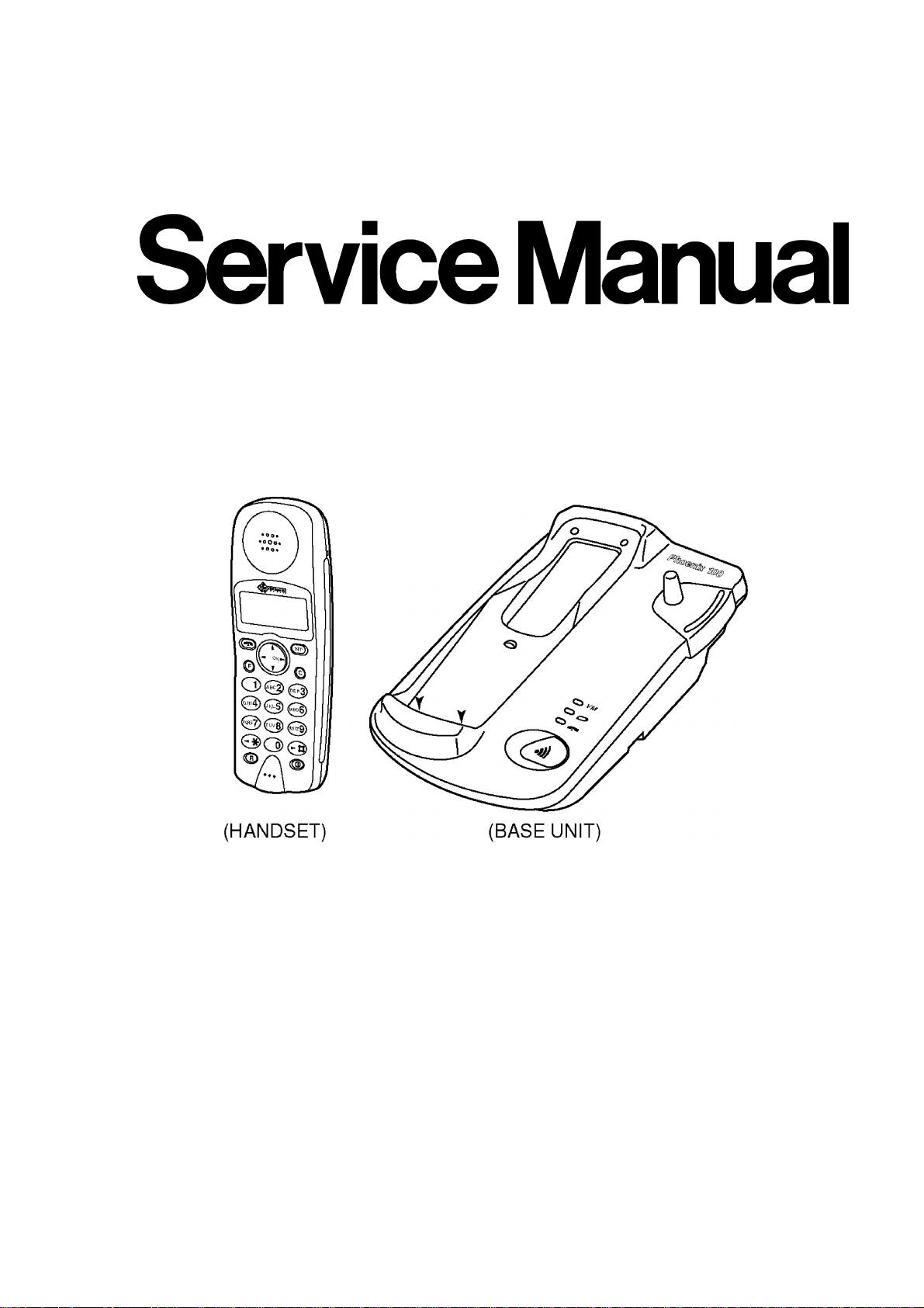
Page 1
ORDER NO. KM40011746C2
Telephone Equipment
PHOENIX100
Digital Cordless Phone
(for Holland)
SPECIFICATIONS
Page 2

1
NOTATION PUBLIC "-//ALDUS//NOTATION TAGGED IMAGE FILE FORMAT//EN"
ENTITY SYSTEM "warning.tif"
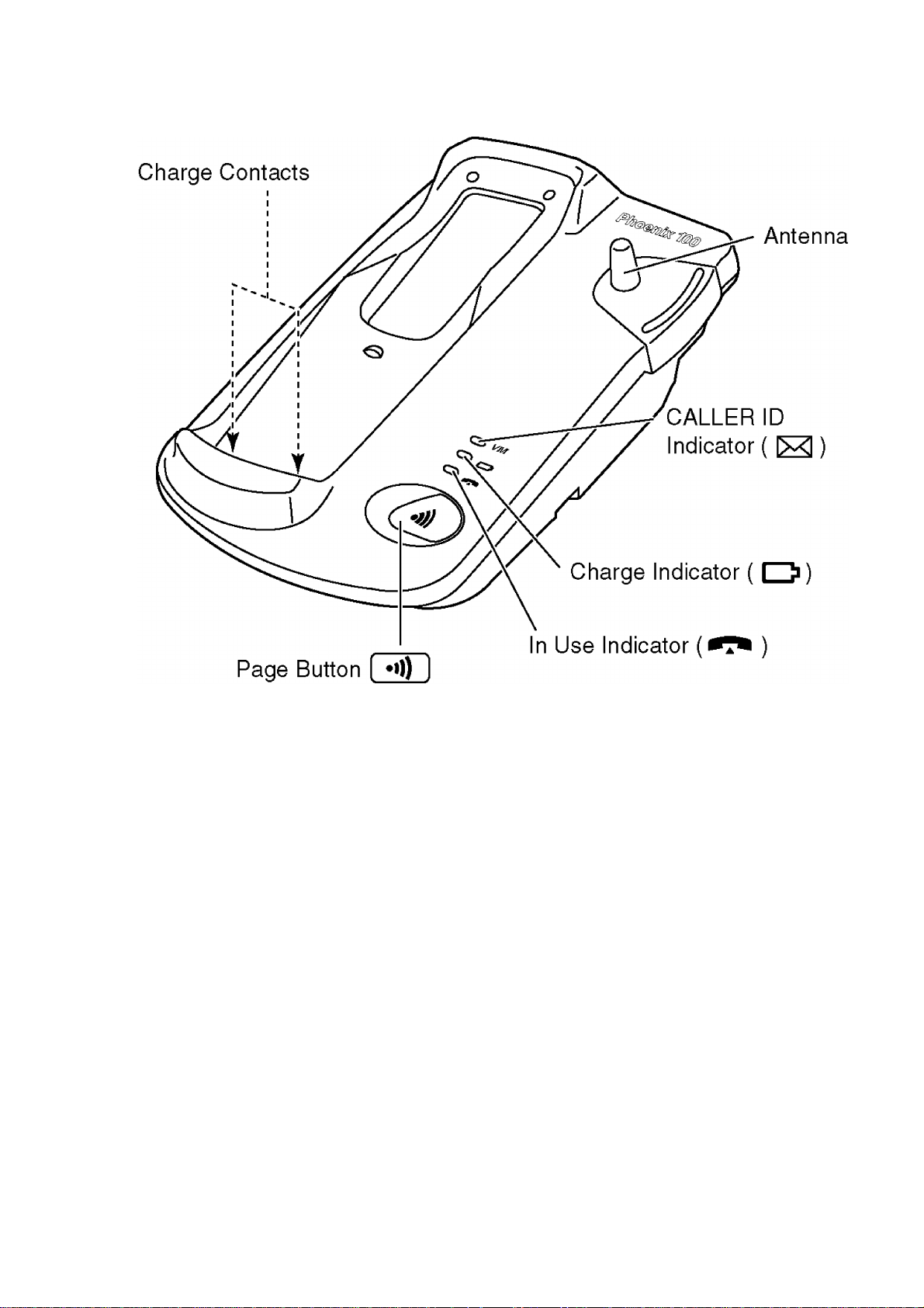
1. LOCATION OF CONTROLS
Base Unit
Fig. 1
Page 3
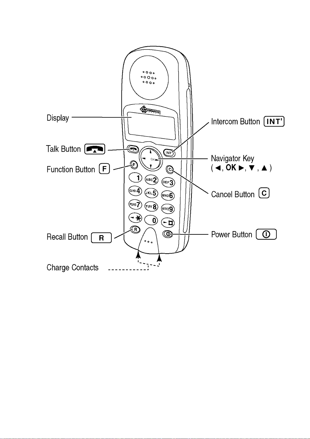
Handset
Fig. 2
Page 4
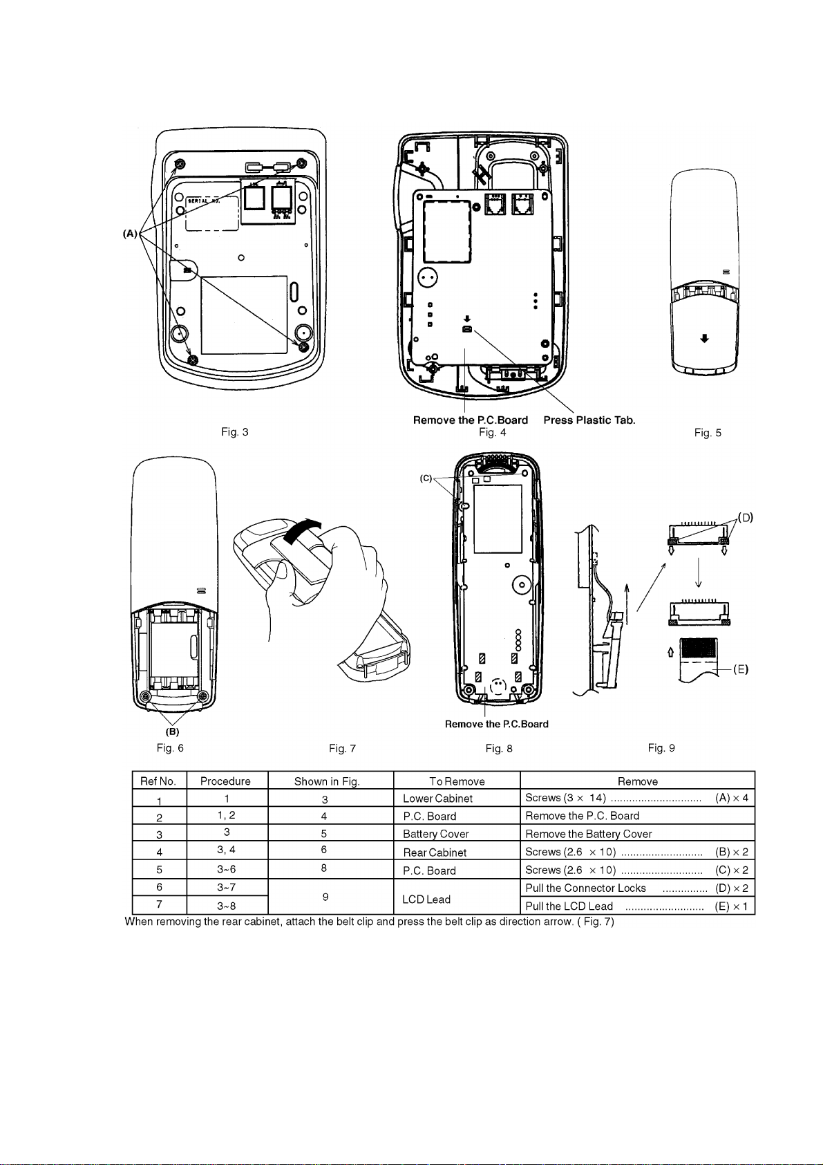
2. DISASSEMBLY INSTRUCUTIONS
Page 5
3. SETTINGS
Page 6
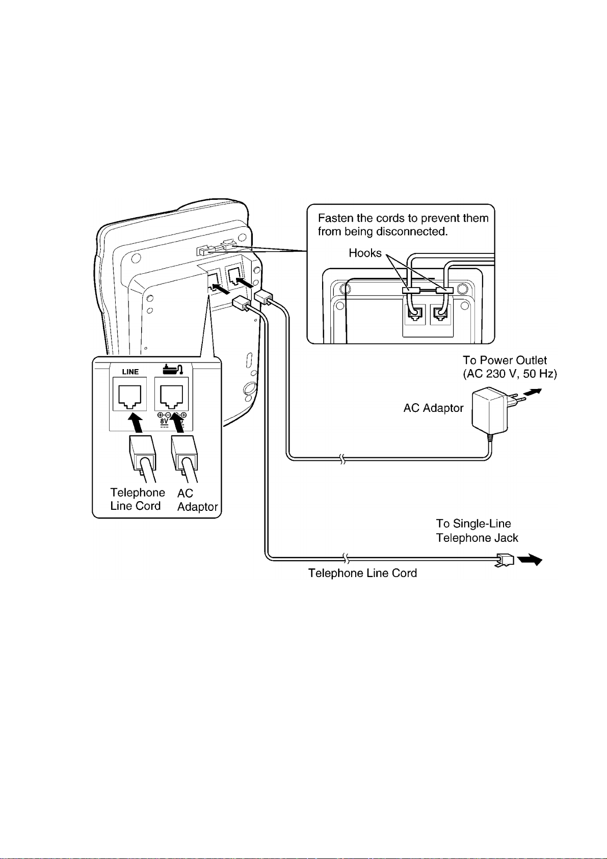
3.1. CONNECTION
Plug in the AC adaptor cord and the telephone line cord to the bottom of the
unit. Then connect the cords as shown.
Fig. 11
- USE ONLY WITH Panasonic AC ADAPTOR KX-TCA11CE.
- Be careful not to confuse the telephone line jack with the AC adaptor jack on
the base unit. If connected improperly, the base unit will not work and
damage may occur.
- The AC adaptor must remain connected at all times. (It is normal for the
adaptor to feel warm during use.)
- The unit will not work during a power failure. We recommend you connect a
standard telephone on the same line for power protection.
Page 7

- If your unit is connected to a PBX which does not support Caller ID services,
you cannot access those services.
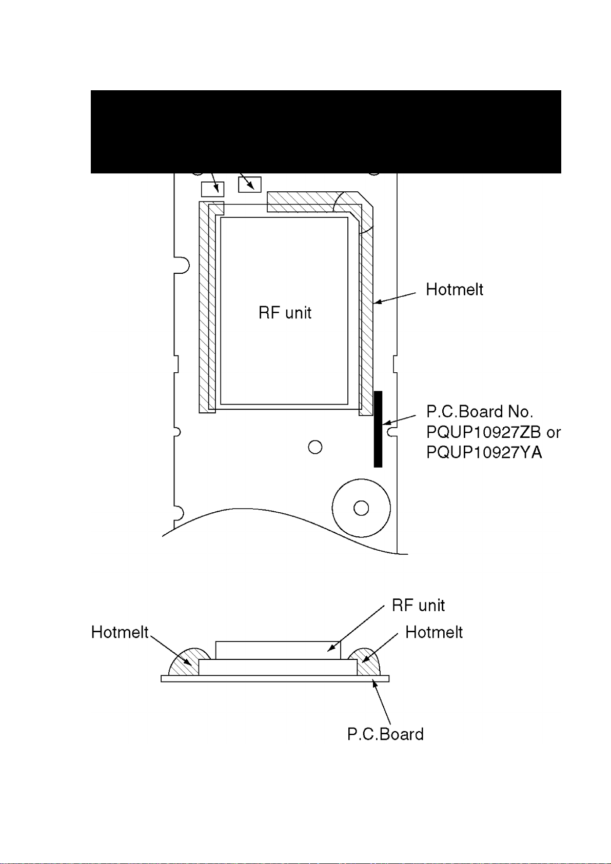
4. HOW TO REPLACE THE RF UNIT OF HANDSET
When replacing the P.C. Board No. PQUP10927ZB and PQUP10927YA, the
hotmelt removing and putting operation is required.
1. Cool the P.C. Board in the freezer for 10 minutes, then remove the hotmelt of
the hatched parts in Fig. 12 with the tip of minus screwdriver.
2. Remove the solder of each pin on RF unit, then remove the RF unit from the
P.C. Board.
3. After soldering the new RF unit on the P.C. Board surely, put the hotmelt on
the hatched part in the Fig. 12.
4. Note:
Above-mentioned hotmelt removing and putting operation is only for the P.C.
Board No. PQUP10927ZB and PQUP10927YA.
5. There is no need of the hotmelt removing and putting operation for the PC
Board No. PQUP10927ZC.
Fig. 12
Page 8
Page 9
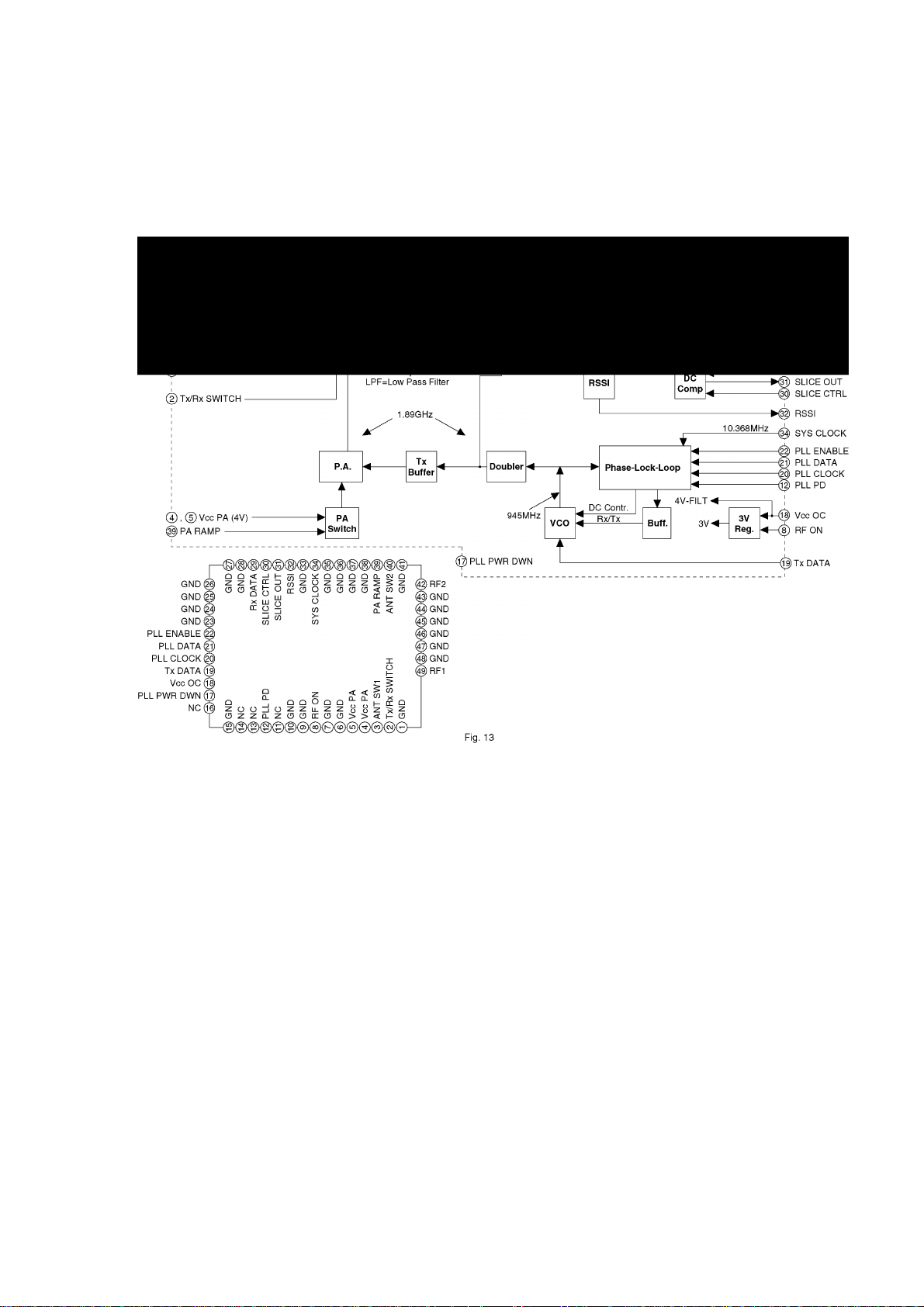
5. BLOCK DIAGRAM RF UNIT (BASE UNIT)
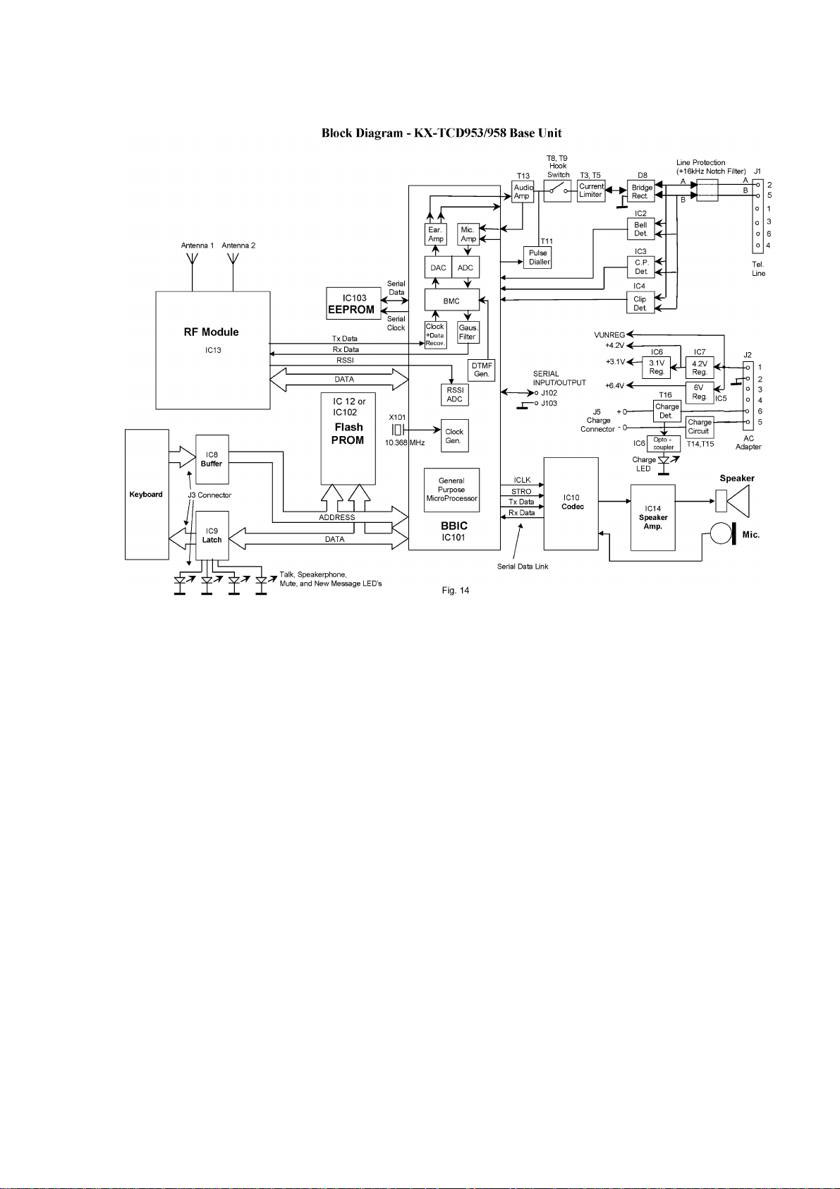
6. BLOCK DIAGRAM BASEBAND SECTION AND LINE
INTERFACE (BASE UNIT)
Page 10
7. CIRCUIT OPERATION (BASE UNIT)
7.1. R.F. SECTION (SEE BLOCK DIAGRAM Fig. 13)
7.2. THE BASE-BAND SECTION (SEE BLOCK DIAGRAM Fig.
14)
7.2.1. INTRODUCTION
The base-band section consists of a base-band integrated circuit (BBIC), a Flash
PROM, an EEPROM, and an AND Gate.
7.2.2. THE BASE-BAND INTEGRATED CIRCUIT (BBIC)
The PQVINSC14424 (IC101) is a CMOS device designed to handle all the audio,
signal and data processing needed in a DECT base unit. It contains a "burst
mode controller” microprocessor which takes care of DECT specific physical
layer and radio section control. It also contains two ADPCM transcoders, a low
Page 11

power 14 bit codec (ADC/DAC), various other ADC´s, DAC´s and timers, a
gaussian filter for the DECT GFSK modulation method, clock and data recovery
circuits, a clock oscillator circuit, a DTMF generator (DSP), an echo suppression
circuit (DSP), and a pair of gain controllable audio amplifiers for line input and
line output and a general purpose microcontroller.
The IC101 interfaces to its external PROM (IC102) via a data/address/control
bus. It connects to the EEPROM via a serial interface, and a second serial
interface is used during manufacture and service to connect to an external
computer.
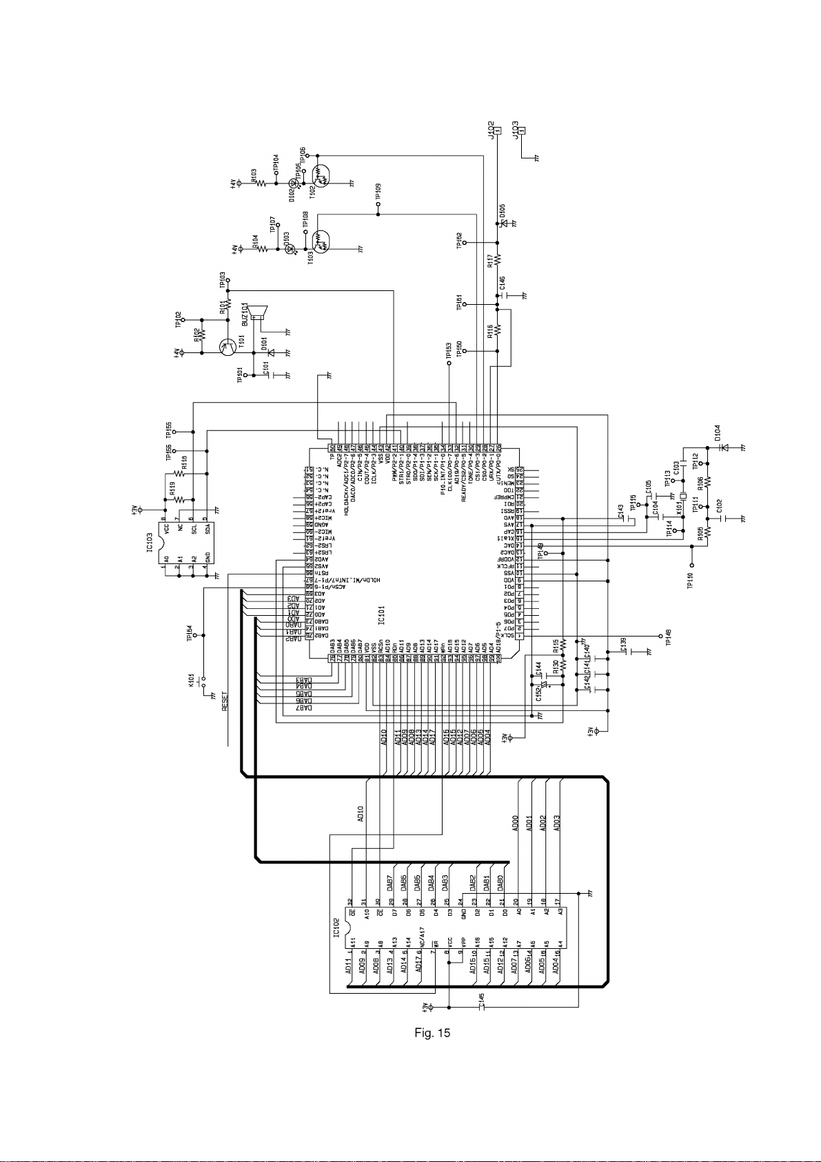
7.2.3. FLASH PROM (SEE Fig. 15)
The 1 Mbit (IC102) Flash PROM contains the operational firmware for the
microcontroller. It is interfaced to the data/address/control bus using address
lines A0 to A16, data lines D0 to D7, and chip select (pin 30), output enable (pin
32), and write (pin 7).
7.2.4. EEPROM (SEE Fig. 15)
The electrically erasable PROM PQVINM4C32L (IC103) is used to store all the
temporary operating parameters for the base (see EEPROM LAYOUT). It uses a
two-line serial data interface with the BBIC, with bi-directional data on pin 5
(TP94), and clock on pin 6 (TP93).
7.2.5. CLOCK GENERATION (SEE Fig. 15)
A single clock generator in the BBIC uses an external crystal X101 to derive all
clock frequencies used in the base. The crystal is tuned to the exact frequency
of 10.368 MHz during manufacture by feeding a DC voltage from a DAC in the
microcontroller (from pin 14 of IC101) to the varicap diode D104 (TP112).
The BBIC provide buffered clock signals RFCLK (pin 11, TP139) at 10.368 MHZ
for the Frequency Synthesizer, which is only active during the PLL lock period.
Other clock is SCLK on pin 1 (3.456MHz). The basic data rate for TRADAT and
RECDAT is 1.152 Mbits/s, which is 10.368 MHs divided by 9. The data rate for the
serial interface to the phase-lock-loop is also 1.152 Mbits/s.
Circuit Diagram
Page 12
Page 13

7.2.6. LOCATOR KEY (SEE Fig. 15)
The keyboard “Locator (Page)” button is connected to pin 68 (TP154) of the
IC101. When pressed the base transmits a message to the handset, which then
beeps.
7.2.7. FACTORY SERIAL PORT (SEE Fig. 15)
In order to communicate with the handset during manufacture and servicing
(using a PC) a serial data link has been provided. Serial data input/output is
provided on J102 (TP151), and a ground is provided on J103. The bi-directional
serial data line is split into two at IC101 pin 27 (input) and pin 26 (output). Data
rate is 9600 baud J103. D105provides ESD protection, and R117 and C146
provide RF de-coupling.
7.2.8. BUZZER CIRCUIT (SEE Fig. 15)
A square-wave signal from IC101 pin 41 (TP103) is used to sound the buzzer via
switching transistor T101 (TP101). Various tones and cadences are used
dependent on function. Buzzer volume is varied by changing the duty cycle of
the drive waveform. D101 provides quenching of back-emf generated when T101
turns off.
7.2.9. OFF HOOK AND CALLER LED´S (SEE Fig. 15)
When the Handset is in “Talk” mode, the Off-Hook LED D102 is switched on by
transistor T102 (on), using a control line from pin 28 of IC101 (TP106). “On the
TCD952 the caller” LED is switched via T103.
7.2.10. AUDIO PATH-RX AUDIO-LINE INPUT (SEE Fig. 16)
Audio from the Line Interface TXAF (TP123) enters the BBIC on pin 58. R111 and
C113 are to balance the line input amplifier, into the ADC part of the codec,
where it is sampled and turned into digital data. The burst mode controller then
processes this raw data (called the B-field) performing encryption and
scrambling, adding the various other fields that go together to produce the GAP
standard DECT frame, assigning to a time slot and channel etc. The data then
passes through the gaussian filter to emerge on pin 22 as TRADAT, (TP132).
7.2.11. AUDIO PATH - TX AUDIO - LINE OUTPUT (SEE Fig. 16)
Audio from the receiver RECDAT enters the BBIC on pin 20 and passes through
the clock recovery circuit. The burst mode controller separates out the B-field
data, and performs de-encryption and de-scrambling as required. It then goes to
Page 14
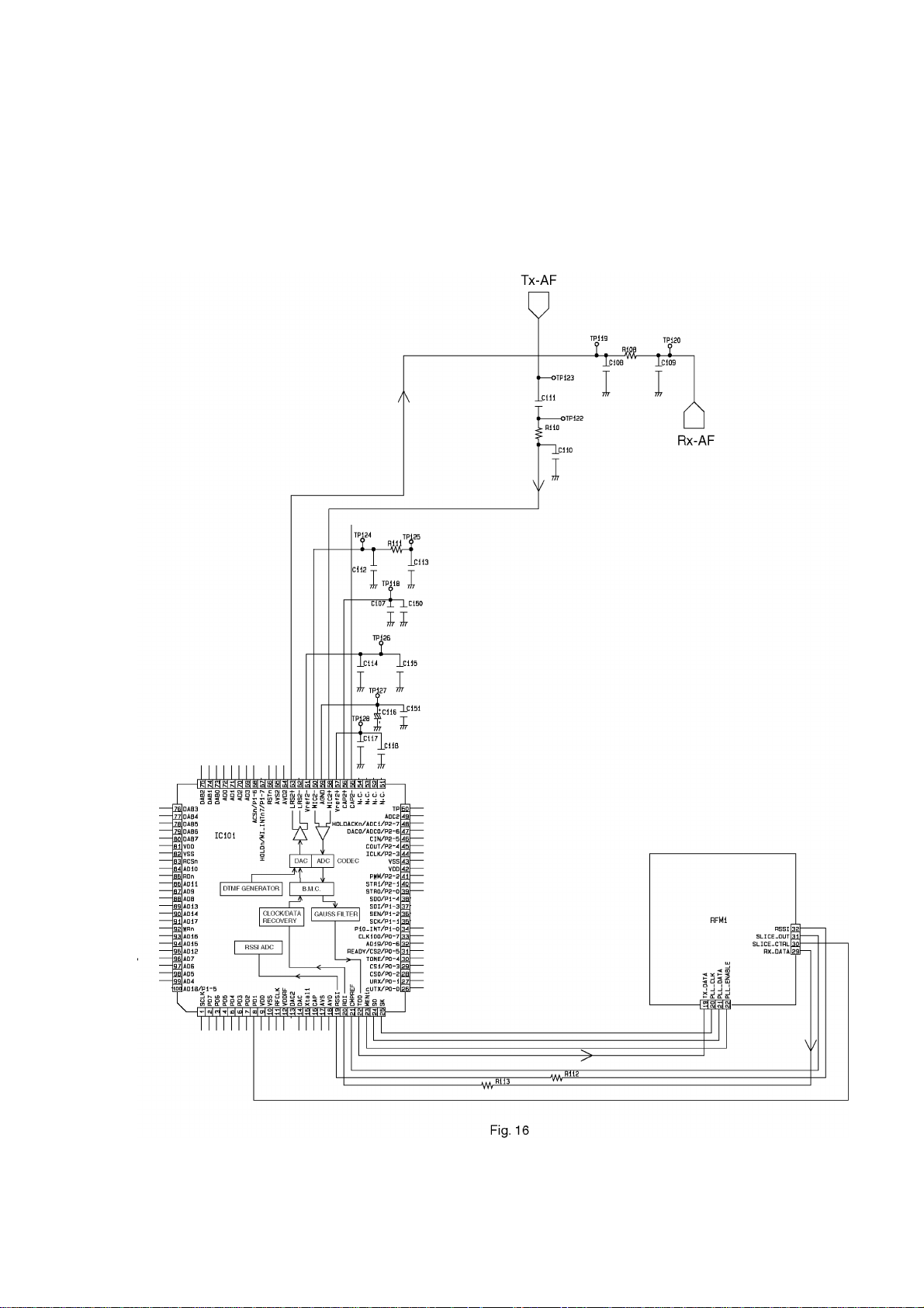
the DAC part of the codec where data is turned back into analogue audio. The
audio signal is amplified by the gain-controlled line output amplifier, and
balanced audio is output on pin 63, and fed as RXAF (TP120) to the Line
Interface.
Circuit Diagram
Page 15

7.3. THE LINE INTERFACE SECTION (SEE BLOCK
DIAGRAM Fig. 15)
7.3.1. INTRODUCTION
This section consists of the telephone line interface, bell detector, hookswitch,
pulse dialing circuits, audio circuits, DC mask & line impedance circuits, power
supplies, and battery charger circuits.
7.3.2. TELEPHONE LINE INTERFACE (SEE Fig. 17)
The telephone line is connected (via 2 or 3 jumpers selected for country of
destination) to a bridge rectifier D8. Surge suppressor SA3 protects against
excessive line voltages. Test points are TP14 (A), TP13 (B), TP21 (S) and TP15
(E). Bridge rectifier D8 provides for lines of either polarity. The output of D8 is
“Line +” (TP50) and “Line -” which is ground.
7.3.3. EARTH RECALL (SEE Fig. 17)
For countries that require Earth Recall facilities, relay RLY1 is provided to short
the E line to the A or B lines. The relay is energised when transistor T2 is
switched on by a high level on the EARTH control line (TP77) from the BB-IC
IC101. D1 will quench the large back-emf voltage that would otherwise occur
across the relay coil when T2 turns off.
7.3.4. BELL DETECTOR (SEE Fig. 17)
The AC ringing signal is detected by optocoupler IC2, using its internal diode in
conjunction with D4. DC from the line is blocked by the wall plug inside. The
other components D2, D3, and R3 reduce current and increase the circuit
impedance in line with national requirements. When ringing is detected IC2 will
turn on, and the RING line (TP76) will be dragged to a low voltage.
Circuit Diagram
Page 16

7.3.5. CLIP CIRCUITS (SEE Fig. 17)
The caller ID signal is detected by IC4.
7.3.6. HOOKSWITCH (AND PULSE DIALING) (SEE Fig. 18)
T8 is the hookswitch, driven by T9. When the phone is “off-hook”, the HOOK
control signal from the BBIC will be a high logic level (+3V), and all both
transistors will be on, thus T8 will “loop” the line. The zenner diode D10
protects transistors T11 to T13 against transient line voltages.
7.3.7. PULSE DIALING (SEE Fig. 18)
During pulse dialing the hookswitch (T8, T9) is used to generate the pulses
using the HOOK control signal, which is set high during pulses. To force the line
impedance low during the “pause” intervals between dial pulses, the
PAUSE-DIAL signal turns on T11, which turns on T12 harder (increases current),
thus reducing line impedance (see 7.3.10. BATTERY CHARGER (SEE Fig. 19))
Page 17

7.3.8. AUDIO CIRCUITS (SEE Fig. 18)
The line output signal from the BBIC RXAF (TP120) is amplified by T13. The
RXAF line is DC coupled to T13 thus making it work as a current limiter (typically
< 8mA). The emitter load of T13 is complex to achieved the correct frequency
response, since the line load (for UK) is also complex. The line input signal
TXAF (TP123) is taken from the junction of R41 and R70. Phase cancellation of
the line output audio occurs at this point, so that only incoming line audio
should be passed to the BBIC on TXAF.
Circuit Diagram
7.3.9. POWER SUPPLIES (SEE Fig. 19)
The AC Adaptor for the KX-TCD952PDB consists of two separate isolated DC
supplies providing a +8 V supply for the base circuitry, and a 9 V supply only for
the charger circuit. The isolation is because the main base circuitry is
connected to the telephone line, so potentially hazardous voltages may be
present, while the charger circuitry has charge contacts that could be touched
by the operator, so the two supplies must be kept separate. The 8 V supply from
the AC Adaptor is connected via J2 pin 1 (TP90) +8 V, and J2 pin 2 (TP89)
ground. The unregulated +8 V supply is fed to the first regulator.This regulator
IC7 provides a regulated output pin 2 (TP91) of +4.0 V (called +4V). The second
regulator IC6 is fed with +4V and provides the stable +3.0V supply (TP95).
During power-up this regulator generates a RESET signal (TP94) which is used
to reset the microcontroller and BBIC.
7.3.10. BATTERY CHARGER (SEE Fig. 19)
The 9 V supply from the AC Adaptor is connected via J2 pin 6 (TP82) positive,
Page 18

and J2 pin 5 (TP78) negative. The constant current battery charger circuit is
made up of T14 and T15 (series pass transistor) and associated components.
Charging detector circuit T16 switches on when a charging current flows
through R64 and D11, and turns on the “Charging” LED D12. The charge
contacts are J5. Charge current flows in via J5 (negative), through T15, R63, AC
Adaptor 9 V supply, R64, D11, and out via J5 (positive).
Circuit Diagram
8. BLOCK DIAGRAM RF UNIT (HANDSET)
Page 19

9. BLOCK DIAGRAM BASE-BAND SECTION
(HANDSET)
Page 20

10. CIRCUIT OPERATION (HANDSET)
10.1. THE BASE-BAND SECTION (SEE BLOCK DIAGRAM
Fig. 21)
10.1.1. INTRODUCTION
The base-band section consists of a base-band integrated circuit (BBIC), a Flash
PROM, an EEPROM, an LCD Display, a Microphone, an Earpiece, and power
supply/battery management circuits.
10.1.2. THE BASE-BAND INTEGRATED CIRCUIT (BBIC)
The National SC14405 BBIC (IC1) is a CMOS device designed to handle all the
audio, signal and data processing needed in a DECT handset. It contains two
microprocessors - one general purpose - while the other ìburst mode controllerî
takes care of DECT specific physical layer and radio section control.The BBIC
also contains the ADPCM transcoders, a low power 14 bit codec (ADC/DAC),
various other ADCís, DACís and timers, a UART for data communication with RF
Page 21

unit, a gaussian filter for the DECT GFSK modulation method, clock and data
recovery circuits, a clock oscillator circuit, a battery management circuit, and a
pair of gaincontrollable amplifiers for the microphone and earpiece.
10.1.3. FLASH PROM (SEE Fig. 22)
The 2 Mbit Flash PROM IC2 contains the operational firmware for the BBIC’s
general purpose microprocessor. It is interfaced to the BBIC using address lines
AD0 to AD17, data lines DAB0 to DAB7, and the chip select (IC1 pin 84), read (IC1
pin 86), and write (IC1 pin 93) control lines.
Fig. 22
Circuit Diagram
10.1.4. LCD DISPLAY, AND DISPLAY DRIVER (SEE Fig. 23)
The LCD display also receives data via a serial interface. Serial data is sent to
LCD display on pin 3 (TP70). The RS signal (pin 1, TP67) is used by the BBIC to
send either commands or data.
Fig. 23
Circuit Diagram
Page 22

10.1.5. AUDIO PATH - TX AUDIO (SEE Fig. 24)
Balanced audio from the microphone (TP40 and TP41) enters the BBIC at pins
61 and 63. A balanced bias voltage for the (“electret” type) microphone is
supplied by the BBIC from pins 60 and 64 via R31 and R32. This supply is
de-coupled by R22, R27, C21, C28, and C22. RF de-coupling of the microphone
signal is provided by R27, C25, R28, C26, R24, R25, and C20. The microphone
audio signals are coupled to the BBIC via C22 and C23, which provide some
high pass filtering.
In the BBIC audio passes through the gain-controlled microphone amplifier, into
the ADC part of the codec, where it is sampled and turned into digital data. The
burst mode controller then processes this raw data (called the B-field)
performing encryption and scrambling, adding the various other fields that go
together to produce the GAP standard DECT frame, assigning to a time slot and
channel etc. The data then passes through the gaussian filter to emerge on pin
20 as TRADAT.
10.1.6. AUDIO PATH - RX AUDIO (SEE Fig. 24)
Audio from the receiver RECDAT (TP54) enters the BBIC on pin 18 and passes
through the clock recovery circuit. The burst mode controller separates out the
B-field data, and performs de-encryption and de-scrambling as required. It then
Page 23

goes to the DAC part of the codec where data is turned back into analogue
audio. The audio signal is amplified by the gain-controlled earpiece amplifier,
and balanced audio is output on pins 65 and 66, and fed to the earpiece (TP31
and TP32). The leads feeding the earpiece are RF de-coupled by C15 to R22,
C17, C16, R23, and C18. C19 provides low pass filtering.
Fig. 24
Circuit Diagram
10.1.7. CLOCK GENERATION (SEE Fig. 25)
A single clock generator in the BBIC uses an external crystal X1 to derive all
clock frequencies used in the handset. The crystal is tuned to the exact
frequency of 10.368 MHz during manufacture by feeding a DC voltage from an
internal DAC (from pin 12) to the varicap diode D12 (TP25). The RFCLK output
(pin 10, TP56) is a buffered clock signal at 10.368 MHz for the Frequency
Synthesizer, that is only active during the PLL lock period (see section 1.3). The
basic data rate for TX-DATA and RX-DATA is 1.152 Mbits/s, which is divided by
9. The data rate for the serial interface to the phase-lock-loop is also 1.152
Mbits/s.
10.1.8. KEYBOARD (SEE Fig. 25)
Page 24

The keyboard “On” button is connected directly to pin 41 of the BBIC (TP10).
When pressed it turns the handset on and off (must be held for off). All other
keys are connected in a row/column matrix. They are scanned in six rows using
scan pulses (only active when keys are pressed) from IC1 pins 28 to 33. The four
key matrix columns are input to the BBIC on pins 31 to 34.
Fig. 25
Circuit Diagram
10.1.9. FACTORY SERIAL PORT (SEE Fig. 21)
Page 25

In order to communicate with the handset during manufacture and servicing
(using a PC) a serial data link has been provided. Serial data input/output is
provided on J6 (TP65), and a ground is provided on J7. The bi-directional serial
data line is split into two at IC1 pin 27 (input) and pin 26 (output). Data rate is
9600 baud or 115.2 kBaud. D13 provides ESD protection, and R37 and C56
provide RF de-coupling.
10.1.10. BUZZER CIRCUIT (SEE Fig. 26)
A square-wave signal from IC1 pin 45 is used to sound the buzzer via switching
transistor T5 (TP22). Various tones and cadences are used dependent on
function. Buzzer volume is varied by changing the duty cycle of the drive
waveform. D11 provides quenching of back-emf generated when T5 turns off.
10.1.11. BATTERY SUPPLY (SEE Fig. 26)
The three cell NiCd/NiMH rechargeable battery supplies the handset via 2A fuse
(actually a coil), and is de-coupled by C3 and C4. It directly supplies T3 in the
baseband section, and also the Tx PA in the RF Section. It also supplies IC1
(de-coupled by C9), and most of the RF Section (VCC-OC) (decupled by R35 and
C47, C48 and VCC-PA).
10.1.12. MAIN 3V REGULATOR (SEE Fig. 26)
The BBIC measures the battery voltage on pins 58 using an internal ADC. If the
battery voltage is below 3.36 V, TC3 is switched to power off mode. R7 and C5
provide a reset pulse (TP84) used for resetting the BBIC when power on. The +3
V supply (TP10) is fed to the BBIC, Flash PROM, EEPROM, and Display Driver.
10.1.13. BATTERY CHARGING CIRCUIT (SEE Fig. 26)
The charge circuit is designed to operate with a constant current charger in the
base. L1, L2, D2 and D4 protect against electro-static discharge (ESD). The
charging current from the base is turned on and off by T1 using a control signal
from the BBIC (pin 39, TP6) via T2. R3 provides initial current in the event of a
totally flat battery, and D6 protects against the high voltage present on the
charge contacts if there is no battery in the handset. R4 and R5 provide a signal
for the BBIC to detect (pin 40) that the handset had been placed on the base
charger. If the handset is off, it will be switched on, and charging will start.
Fig. 26
Circuit Diagram
Page 26

11. ADJUSTMENT (BASE UNIT)
Adjustment objectives
item Symptom Remedy
frequency Synchronization with the portable handset is lost
immediately.
No link is established.
Perform the adjustments
described in item(1).
Page 27

Tools required for adjustments
- Frequency counter
- Personal computer
- Serial communication tool
- Test software (batch files)
- Line simulator
- Oscillator
- Audio level meter
Item(1)
1. Connect the serial link to test computer to J102 (serial data) and J103 (GND).
2. Connect the AC adaptor.
3. Connect the frequency counter to TP148 (SCLK) and J103 (GND).
4. Send batch file “FIXFREQ.BAT”
5. Send “SETFREQ.BAT” to set the clock frequency. The default value is 80.
Increase the value to increase the frequency. The clock frequency must be
3,456 kHz ± 0.007 kHz.
12. ADJUSTMENT (HANDSET)
Adjustment objectives
item Symptom Remedy
frequency Synchronization with the portable handset is lost
immediately.
No link is established.
battery The communication (standby) times is short. Perform the adjustments
The low battery display period is too long or too
short.
Perform the adjustments
described in item(1).
described in item(2).
Tools required for adjustments
Page 28

- Frequency counter
- Power supply unit (DC 3V~5V, 1A)
- Personal computer
- Serial communication tool
- Test software (batch files)
Item(1)
1. Connect the serial link to test computer to J6 (serial data) and J8 (GND).
2. Turn off power for the base unit.
3. Input a 3.9V supply to the handset J5 (+) and J8 (GND).
4. Connect the frequency counter to TP56 and J8 (GND).
5. Press the “power on” button.
6. Send batch file “FIXFREQ.BAT”.
7. Use batch file “SETFREQ.BAT” to set the clock frequency. The default value
is 80. Increase the value to increase the frequency and vice-versa. The clock
frequency must be 10,368.000 kHz ± 0.02 kHz.
Item(2)
1. Connect the serial link to test computer for J6 (serial data) and J8 (GND).
2. Set the battery voltage to 4.6V at J1 and J2.
3. Press the “power on” button.
4. Send batch file “READBATT.BAT”. The returned hex value is M2.
5. Send batch file “WRTBATT.BAT M2”.
6. Set the battery voltage to 3.5V at J5 (+).
7. Send batch file “READBATT.BAT”. The returned hex value is M1.
8. Send batch file “WRTBATT.BAT M1”.
9. Calculate the low value 2 level:
10. Send “WRTBATT.BAT M3”.
Page 29

13. CHECK PROCEDURE (BASE UNIT)
13.1. TEST EQUIPMENT REQUIRED AND EQUIPMENT
SETUP
13.2. INITIAL POWER + BBIC TESTS
1. Turn on the 10V supply.
2. Check for approx. 70 mA current on the 10V supply.
3. Check the 4V supply voltage (TP91). It must be 3.88 ±0.2V.
4. Check the 3.3V supply voltage (TP95). It must be 3.0 ±0.2V.
5. Connect SCLK (TP148) to CH.1 on the scope.
6. Check if the clock waveform is 3,456 kHz.
7. Send batch file “SELF TEST”.
13.3. SET THE CLOCK FREQUENCY
Page 30

1. Send batch file “FIX FREQ”.
2. Check for approx. 90 mA current on the 8V supply.
3. Transfer SCLK (TP148) to the frequency counter.
4. Send batch file “SETFREQ nn” to set the clock frequency. The default value of
nn is 80. Increase the value to increase the frequency and vice-versa. The
clock frequency must be 3,456 kHz ( ± 0.007 kHz).
13.4. QUICK Tx CHECK
1. Set the CMD60 to MODULE TEST.
2. Send batch file “H”.
3. Confidence check of Power (NTP): it must be +20 to +25 dBm.
4. Confidence check of Frequency Offset: it must be 0 ± 40 kHz.
5. Confidence check of Deviation of B field Data Type 01010101: it must be 207
to 270 kHz.
13.5. LOOPBACK TEST
1. Set the CMD60 to MANUAL TEST.
2. Set the CMD60 TRAFFIC CARRIER to 5.
3. Send batch file “TESTMODE”.
4. On the CMD60, press “SETUP CONNECT”.
5. Check the Power (NTP): It must be +20 to +25 dBm.
6. Press MODULATION.
7. Set Data Type to “Fig. 27”.
8. Check the Frequency Drift: it must be 0 ± 45 kHz/ms.
9. Check the Frequency Offset: it must be 0 ± 40 kHz.
10. Send batch file ìWREE 00 16 nmî to adjust the Deviation (Max. B Field) with
Data Type: 01010101. Increase the value nm to increase the Deviation and
vice-versa. The least significant digit (m) of the value must be 1 (i.e. only the
values 31, 41, 51, 61 etc. are allowed). The Deviation must be 207 to 270 kHz.
11. Check the Deviation (Max. ± B Field) with Data Type “Fig. 27”: it must be 202
to 404 kHz.
12. Press MENU UP.
13. Press POWER RAMP.
Page 31

14. Check the Burst fits mask.
15. Press MENU UP.
16. Press BER.
17. Note the Sensitivity (reduce RF LEVEL for a BER of approx. 1000ppm) : the
RF LEVEL must be < - 90 dBm.
18. Press MENU UP.
19. Press BEARER RELEASE.
Note:
These tests can be repeated on Traffic Carriers 5 and 9.
13.6. TELEPHONE LINE TESTS
1. Connect the tel line from the base under test to the line simulator.
2. Send batch file “OFFHOOK”.
3. Check if the green “In-Use” LED is on.
4. Set the line current to 40 mA on the line simulator.
5. Send batch file “ONHOOK”.
6. Check that the line current is 0 ± 0.5 mA.
7. Check if the green “In-Use” LED is off.
8. Send batch file “OFFHOOK”.
9. Check the DC Voltage on TP45. It must be 9.5 ± 0.5V.
10. Send batch file “LINIMP 1”.
11. Check the DC Voltage on TP45. It must be < 3.5V.
12. Send batch file “LINIMP 0”.
13. Send batch file “PULDIAL”.
14. Observe on the line simulator current meter that 5 dial pulses are output
causing the current to reduce to approx. 20mA.
15. Send batch file “STRTDTMF”.
16. Check on the scope that a DTMF waveform is output on that tel line.
17. Send batch file “STOPDTMF”.
18. Disconnect the tel line from the base under test to the line simulator.nm
19. Connect the “Bell” Oscillator to the tel line.
20. Set the “Bell” Oscillator voltage to 32V RMS 23Hz.
Page 32

21. Send batch file “RINGDET”.
22. Check that the ringing voltage has been detected (1 = detected).
13.7. CHARGE CURRENT TEST
1. Connect the 11V supply to J2 pin 6 (+) and J2 pin 5 (-).
2. Connect the ammeter with a series load resistor of 56ΩΩ/2 W to J3 (+) and J4 (-).
3. Switch on the 11V supply.
4. Check the Charge Voltage to J3 and J4 9.5 ± 0.5 V.
5. Switch off the 11V supply.
6. Connect the 11V supply to the “11V Supply” sockets on the test jig.
14. CHECK PROCEDURE (HANDSET)
14.1. TEST EQUIPMENT REQUIRED AND EQUIPMENT
SETUP
NOTATION PUBLIC "-//ALDUS//NOTATION TAGGED IMAGE FILE FORMAT//EN"
ENTITY SYSTEM "14_01_01.tif"
14.2. INITIAL POWER + BBIC TESTS
1. Turn on the 3.9V supply.
2. Press the “Power-on” button.
3. Check for a “beep” and approx 80 mA current on the 3.9V supply.
4. Check the 3.0V supply voltage (TP10). It must be 2.85 +/- 0.3.
5. Connect RFCLK (TP56) to CH.1 on the scope. Send batch file RFCLK1.
6. Check if the clock waveform is 10,368.000 kHz, +/- 40Hz.
7. Send batch file ”SELF TEST”. The first 4 digits are FLASH ROM checksum,
the next 2 digits are RAM test, and must be 00.
14.3. SET CLOCK FREQUENCY
1. Send batch file “RFCLK1”.
2. Connect RFCLK (TP56) to the frequency counter.
Page 33

3. Send batch file “SET FREQ nn” to set the clock frequency. The default value
of nn is 80. Increase the value to increase the frequency. The clock frequency
must be 10,368.000 kHz ± 0.04 kHz.
14.4. QUICK Tx CHECK
1. Set the CMD60 to MODULE TEST.
2. Send batch file “H”.
3. Confidence check of Power (NTP): must be +20 to +25 dBm.
4. Confidence check of Frequency Offset: must be 0 ± 40 kHz.
5. Confidence check of Deviation of B field Data Type 01010101: must be 207 to
270 kHz.
14.5. LOOPBACK TEST
1. Set the CMD60 to MANUAL TEST.
2. Set the CMD60 TRAFFIC CARRIER to 5.
3. Send batch file “TESTMODE”.
4. On the CMD60 press “SETUP CONNECT”.
5. Check Power (NTP): must be +20 to +25 dBm.
6. Press MODULATION.
7. Set Data Type to “Fig. 27”.
8. Check the Frequency Drift: must be 0 ± 45 kHz/ms.
9. Check the Frequency Offset: must be 0 ± 40 kHz.
10. Send batch file ìWREE 00 16 nmî to adjust the Deviation (Max. B Field) with
Data Type: 01010101. Increase the value nm to increase the Deviation and
vice-versa. The least significant digit (m) of the value must be 1 (i.e. only the
values 31, 41, 51, 61 etc. are allowed). The Deviation must be 207 to 270 kHz
11. Check the Deviation (Max. ± B Field) with Data Type “Fig. 27”: must be 201 to
404 kHz.
12. Press MENU UP.
13. Press POWER RAMP
14. Check the Burst fits mask.
15. Press MENU UP.
16. Press BER.
Page 34

17. Note the Sensitivity (reduce the RF LEVEL for a BER of approx. 1000ppm) :
RF LEVEL must be < - 90 dBm
18. Press MENU UP.
19. Press BEARER RELEASE.
Note:
These tests can be repeated on Traffic Carriers 0 and 9.
15. TROUBLESHOOTING GUIDE
15.1. HANDSET: DOES NOT OPERATE
NOTATION PUBLIC "-//ALDUS//NOTATION TAGGED IMAGE FILE FORMAT//EN"
ENTITY SYSTEM "15_01_01.tif"
NOTATION PUBLIC "-//ALDUS//NOTATION TAGGED IMAGE FILE FORMAT//EN"
ENTITY SYSTEM "15_01_02.tif"
15.2. HANDSET: LINK
NOTATION PUBLIC "-//ALDUS//NOTATION TAGGED IMAGE FILE FORMAT//EN"
ENTITY SYSTEM "15_02_01.tif"
NOTATION PUBLIC "-//ALDUS//NOTATION TAGGED IMAGE FILE FORMAT//EN"
ENTITY SYSTEM "15_02_02.tif"
NOTATION PUBLIC "-//ALDUS//NOTATION TAGGED IMAGE FILE FORMAT//EN"
ENTITY SYSTEM "15_02_03.tif"
15.3. HANDSET: DOES NOT LINK
NOTATION PUBLIC "-//ALDUS//NOTATION TAGGED IMAGE FILE FORMAT//EN"
ENTITY SYSTEM "15_03_01.tif"
15.4. BASE UNIT: DOES NOT CHARGE
NOTATION PUBLIC "-//ALDUS//NOTATION TAGGED IMAGE FILE FORMAT//EN"
ENTITY SYSTEM "15_04_01.tif"
15.5. HANDSET: DOES NOT CHARGE
Page 35

Refer to the simplified manual (cover) for other areas.
Notes:
1. The marking (RTL) indicates that the Retention Time is limited for this item.
After the discontinuation of this assembly in production, the item will
continue to be available for a specific period of time. The retention period of
availability is dependent on the type of assembly, and in accordance with the
laws governing parts and product retention.
After the end of this period, the assembly will no longer be available.
2. Important safety notice
Components identified by mark have special characteristics important for
safety. When replacing any of these components, use only manufacture´s
specified parts.
3. The S mark indicates service standard parts and may differ from production
parts.
4. RESISTORS & CAPACITORS
Unless otherwise specified;
All resistors are in ohms (ΩΩ) k = 1000 ΩΩ, M = 1000kΩΩ
All capacitors are in MICRO FARADS (µµF) P=µµµµF
*Type & Wattage of Resistor
Page 36

19.1. Base Unit
19.1.1. CABINET AND ELECTRICAL PARTS
Ref. No. Part No. Part Name & Description Remarks
1 PQBC10270Z1 PAGE BUTTON S
2 PQHR10648Y LED LENDS
3 PQJT10165Z BATTERY TERMINAL
4 PQKM10369T1 UPPER CABINET S
5 PQSA10078Z ANTENNA
6 PQSA10079Z ANTENNA
7 PQSX10099Z RUBBER SWITCH
8 PQYF10146Z2 LOWER CABINET S
9 PQGT14464Z NAME PLATE
19.1.2. MAIN P.C.BOARD PARTS
Page 37

Ref. No. Part No. Part Name & Description Remarks
PCB1 PQWPCDPX100H MAIN P. C. BOARD ASS´Y (RTL)
(ICS)
IC2 PQVIPC357CN IC
IC4 PQVILMV321M5 IC
IC6 PQVIMC295130 IC
IC7 PQVILM1117MP IC
IC101 PQVINS14424V IC
IC102 PQWICDPX100H IC
IC103 PQVIT2432WM6 IC
(TRANSISTORS)
T4 PQVTBF822T7 TRANSISTOR(SI)
T6 2SA1037K TRANSISTOR(SI)
T7 PQVTBCP5216T TRAMSISTOR(SI)
T8 2SA1807NT TRANSISTOR(SI)
T9 PQVTBF822T7 TRANSISTOR(SI)
T13 2SD1994A TRANSISTOR(SI)
T14 2SD601A TRANSISTOR(SI)
T15 2SD1664Q TRANSISTOR(SI)
T16 2SA1037K TRANSISTOR(SI)
T101 PQVTBC80725T TRANSISTOR(SI) S
T102 UN521 TRANSISTOR(SI) S
T103 UN521 TRANSISTOR(SI) S
(DIODES)
D2 PQVDBZV55C02 DIODE(SI)
D3 PQVDBZV55C02 DIODE(SI)
D4 MA110 DIODE(SI)
D8 PQVDS1ZB60F1 DIODE(SI)
D10 MA1Z300 DIODE(SI)
D11 MA112 DIODE(SI)
D13 MA8180 DIODE(SI)
D101 MA110 DIODE(SI)
D104 PQVDHVU359 DIODE(SI)
D105 MA8047 DIODE(SI)
(LEDS)
D12 LNJ211R8ARU LED
D102 LNJ311G8TRU LED
D103 LNJ311G8TRU LED
(JACKS)
J1 PQJJ1T018Z JACK/SOCKET
J2 PQJJ1T019Z JACK/SOCKET
(OTHERS)
BUZ1 PQEFBC1211B BUZZER S
SA3 PQVDDSS301L VARISTOR
X101 PQVCF1036N4Z CRYSTAL OSCILLATOR
J5 PQJP02A85Z CONNECTOR
(RESISTORS)
R3 PQ4R18XJ472 4.7k
R4 ERJ3GEYJ103 10k
R5 PQ4R18XJ565 5.6M
R6 ERJ3GEYJ334 330k
R7 PQ4R18XJ565 5.6M
R8 ERJ3GEYJ334 330k
R13 ERJ3GEYJ223 22k
R14 ERJ3GEYJ223 22k
Page 38

Ref. No. Part No. Part Name & Description Remarks
R19 ERJ3GEYJ394 390k
R20 ERJ3GEYJ393 39k
R21 ERJ3GEYJ394 390k
R22 ERJ3GEYJ104 100k
R23 PQ4R18XJ104 100k
R24 PQ4R10XJ202 2k
R25 PQ4R10XJ000 0
R26 ERJ3GEYJ103 10k
R27 ERJ3GEYJ222 2.2k
R31 ERJ3GEYJ130 13
R32 PQ4R18XJ562 5.6k
R33 ERJ1WYJ152 1.5k
R34 ERJ1WYJ152 1.5k
R35 ERJ3GEYJ104 100k
R36 PQ4R18XJ272 2.7k
R39 ERJ3GEYJ103 10k
R40 ERJ3GEYJ222 2.2k
R41 ERJ3GEYJ333 33k
R43 ERJ3GEYJ560 56
R53 ERJ3GEY0R00 0
R54 ERJ3GEYJ273 27k
R55 ERJ3GEYJ223 22k
R56 ERJ12YJ390 39
R57 ERJ14YJ8R2 8.2
R58 ERJ3GEYJ473 47k
R59 ERJ3GEYJ331 330
R60 ERJ3GEYJ152
R61 ERJ3GEYJ102 1k
R62 ERJ3GEYJ101 100
R63 PQ4R10XJ8R2 8.2
R64 PQ4R10XJ1R5 1.5
R65 ERJ3GEYJ101 100
R66 PQ4R10XJ122 1.2k
R67 ERJ3GEYJ102 1k
R68 ERJ3GEYJ202 2k
R69 ERJ3GEYJ224 220k
R70 ERJ3GEYJ332 3.3k
R101 ERJ3GEYJ102 1k
R102 ERJ3GEYJ103 10k
R103 ERJ3GEYJ151 150
R104 ERJ3GEYJ151 150
R105 ERJ3GEYJ105 1M
R106 ERJ3GEYJ105 1M
R107 ERJ3GEYJ101 100
R108 ERJ3GEYJ560 56
R110 ERJ3GEYJ101 100
R111 ERJ3GEYJ101 100
R112 ERJ3GEYJ273 27k
R113 ERJ3GEYJ332 3.3k
R114 ERJ3GEYJ1R0 1
R115 ERJ3GEYJ100 10
R116 ERJ3GEYJ102 1k
R117 ERJ3GEYJ101 100
R118 ERJ3GEYJ103 10k
1.5k
Page 39

Ref. No. Part No. Part Name & Description Remarks
R119 ERJ3GEYJ103 10k
R120 ERJ3GEYJ103 10k
R121 ERJ3GEYJ222 2.2k
R122 ERJ3GEYJ100 10
R130 ERJ3GEYJ100 10
R135 ERJ3GEYJ0R00 0
R136 ERJ3GEYJ222 2.2k
R422 ERDS1VJ000 0
R519 ERDS1VJ000 0
JMP5 PQ4R10XJ000 0
JMP8 PQ4R10XJ000 0
JMP19 PQ4R10XJ000 0
JMP20 PQ4R10XJ000 0
JMP22 PQ4R10XJ000 0
JMP204 ERJ3GEY0R00 0
JMP205 ERJ3GEY0R00 0
JMP206 ERJ3GEY0R00 0
(CAPACITORS)
C1 ECUV1C104KBV 0.1
C2 ECQE2474KF 0.47
C3 ECUV1H102KBV 0.001
C4 ECUV1H102KBV 0.001
C10 PQCUV1C105ZF 1
C12 ECUV2H102KB 0.001
C13 ECUV1H102KBV 0.001
C14 ECUV2H102KB 0.001
C15 ECUV1H102KBV 0.001
C16 ECUV2H681KB 680P
C17 ECUV2H681KB 680P
C18 ECUV2H681KB 680P
C19 ECEA2EUR47 0.47
C21 ECEA1HKS100 10
C22
C25 ECUV1H100DCV 10P
C27 ECUV1H472KBV 0.0047
C29 PQCUV1C224KB 0.22
C33 ECUV1C104KBV 0.1
C34 PQCUV1H104ZT 0.1 S
C35 PQCUV1H683KB 0.068
C36 ECEA1HKS2R2 2.2
C38 ECUV1H103KBV 0.01
C39 ECUV1C105KB 1
C40 ECEA1CK101 100 S
C41 ECUV1H100DCV 10P
C42 ECEA1CK101 100 S
C43 PQCUV1C224KB 0.22
C44 ECUV1H100DCV 10P
C45 ECEA0JK221 220 S
C47 ECUV1C225ZF 2.2
C48 ECUV1C225ZF 2.2
C101 ECUV1H101JCV 100P
C102 ECUV1H103KBV 0.01
C103 ECUV1H102KBV 0.001
C104 ECUV1H390JCV 39P
ECUV1H103KBV 0.01
Page 40

Ref. No. Part No. Part Name & Description Remarks
C105 ECUV1H390JCV 39P
C106 PQCUV1C224KB 0.22
C107 PQCUV1C105ZF 1
C108 ECUV1H100DCV 10P
C109 PQCUV1C224KB 0.22
C110 ECUV1H100DCV 10P
C111 ECUV1C104KBV 0.1
C112 ECUV1H100DCV 10P
C113 ECUV1C104KBV 0.1
C114 PQCUV1C105ZF 1
C115 ECUV1H100DCV 10P
C116 ECST0JY106 10
C117 PQCUV1C105ZF 1
C118 ECUV1H100DCV 10P
C123 ECUV1H102KBV 0.001
C125 PQCUV1H681JC 680P
C136 PQCUV1C224KB 0.22
C137 ECUV1H100DCV 10P
C139 ECUV1C104KBV 0.1
C140 ECUV1C104KBV 0.1
C141 ECUV1C104KBV 0.1
C142 ECUV1C104KBV 0.1
C143 ECUV1C104KBV 0.1
C144 ECUV1C104KBV 0.1
C145 ECUV1C104KBV 0.1
C146 ECUV1H101JCV 100P
C147 ECUV1H220JCV 22P
C148 ECUV1H220JCV 22P
C150 ECUV1H100DCV 10P
C151 ECUV1H100DCV 10P
C152 ECST0JY106 10
C156 PQCUV1H683KB 0.068
C160 ECUV1H100DCV 10P
C161 ECUV1H100DCV 10P
C162 ECUV1H100DCV 10P
R49 ECUV1H100DCV 10P
RF UNIT PARTS
RFM1 PQLZ10008Z RF BLOCK
19.2. Handset
19.2.1. CABINET AND ELECTRICAL PARTS
Page 41

Ref. No. Part No. Part Name & Description Remarks
101 PQAX3P25Z SPEAKER
102 PQBX10324Y2 PUSH BUTTON S
103 PQGT14463Z NAME PLATE
104 PQGP10145X2 LCD PANEL S
105 PQHG10486Z RINGER RUBBER
106 PQHR10693Z LCD REFLECTOR
107 PQHR10649Y LCD HOLDER
108 PQHR10651Z LCD SPONGE
109 PQHS10342Z SPEAKER NET
110 PQHX10861Z REFLECTOR SHEET
111 PQHX10862Z LCD COVER SHEET
112 PQJC10035Z BATTERY TERMINAL
113 PQJC10036Z BATTERY TERMINAL
114 PQJC10037Z BATTERY TERMINAL
115 PQJC904Y BATTERY TERMINAL
116 PQJT10143Z BATTERY TERMINAL
117 PQKM10370W2 FRONT CABINET S
118 PQSA10085Y ANTENNA
119 PQSX10100Y KEYBOARD SWITCH
120 PQYF10186Z1 REAR CABINET S
19.2.2. MAIN P.C.BOARD PARTS
Ref. No. Part No. Part Name & Description Remarks
PCB100 PQWPTCD955GR MAIN P. C. BOARD ASS´Y (RTL)
(ICS)
IC1 PQVI14405AKS IC
IC2 PQWITCD955GR IC
(TRANSISTORS)
T1 PQVTBC80825T TRANSISTOR(SI) S
T2 UN521 TRANSISTOR(SI) S
T3 PQVTBC80825T TRANSISTOR(SI) S
T4 2SC2412K TRANSISTOR(SI)
T5 PQVTBC81825T TRANSISTOR(SI) S
(DIODES)
D1 PQVDBYD17D DIODE(SI)
D2 PQVDBZD27C18 DIODE(SI) S
D3 MA112 DIODE(SI)
D4 PQVDBZD27C18 DIODE(SI) S
D5 MA112 DIODE(SI)
D6 PQVDBZD27C56 DIODE(SI) S
D7 PQVDHRU0203A DIODE(SI) S
D8 PQVDSML310MT DIODE(SI) S
D9 PQVDSML310MT DIODE(SI) S
D10 PQVDSML310MT DIODE(SI) S
D11 MA110 DIODE(SI)
D12 PQVDHVU359 DIODE(SI)
D13 MA8047 DIODE(SI)
(COILS)
F1 PQLQR2M5N6K COIL
L1 ELJPA100KF COIL
L2 ELJPA100KF COIL
Page 42

Ref. No. Part No. Part Name & Description Remarks
(OTHERS)
A101(+) PQJT10152Y ANTENNA
A101(-) PQJT10152Y ANTENNA
LS2(+) PQJT10161Z SPEAKER TERMIANL
LS2(-) PQJT10161Z SPEAKER TERMIANL
J1 PQJT10090Z BATTERY TERMINAL S
J2 PQJT10090Z BATTERY TERMINAL S
J3 PQJT10090Z BATTERY TERMINAL S
J4 PQJT10090Z BATTERY TERMINAL S
BZ1 PQEFBDB111GP BUZZER
J10 PQJS18A96Z CONNECTOR
X1 PQVCF1036N3Z CRYSTAL OSCILLATOR
M1 PQJM146Z MICROPHONE
LCD LNY163C01 LIQUID CRYSTAL DISPLAY
(RESISTORS)
R1 ERJ3GEYJ103 10K
R2 PQ4R10XJ122 1.2K
R3 PQ4R18XJ471 470
R4 ERJ3GEYJ682 6.8K
R5 ERJ3GEYJ103 10K
R6 ERJ3GEYJ153 15K
R7 ERJ3GEYJ104 100K
R8 ERJ3GEYJ270 27
R9 ERJ3GEYJ270 27
R10 ERJ3GEYJ270 27
R11 ERJ3GEYJ682 6.8K
R12 ERJ3GEYJ103 10K
R13 PQ4R10XJ100 10
R14 ERJ3GEYJ563 56K
R15 ERJ3GEYJ104 100K
R16 ERJ3GEYJ563 56K
R17 ERJ3GEYJ104 100K
R18 ERJ3GEYJ102 1K
R19 ERJ3GEYJ102 1K
R20 ERJ3GEYJ105 1M
R21 ERJ3GEYJ105 1M
R22 ERJ3GEYJ100 10
R23 ERJ3GEYJ100 10
R24 ERJ3GEYJ101 100
R25 ERJ3GEYJ101 100
R27 ERJ3GEYJ101 100
R28 ERJ3GEYJ101 100
R29 ERJ3GEYJ471 470
R30 ERJ3GEYJ471 470
R31 ERJ3GEYJ102 1K
R32 ERJ3GEYJ102 1K
R33 ERJ3GEYJ822 8.2K
R34 ERJ3GEYJ332 3.3K
R35 ERJ3GEYJ1R0 1
R36 ERJ3GEYJ100 10
R37 ERJ3GEYJ102 1K
R38 ERJ3GEYJ101 100
R39 ERJ3GEYF824 820K
R40 ERJ3GEYF434 430K
Page 43

Ref. No. Part No. Part Name & Description Remarks
R44 ERJ3GEYJ103 10K
R46 ERJ3GEYJ224 220K
R49 ERJ3GEYJ104 100K
R50 ERJ3GEYJ563 56K
R51 ERJ3GEYJ104 100K
(CAPACITORS)
C1 PQCUV1E104MD 0.1
C2 ECUV1C104KBV 0.1
C3 ECEV1AA101 100
C4 ECUV1H100DCV 10P
C5 PQCUV1C224KB 0.22
C6 ECUV1H100DCV 10P
C7 PQCUV1C105ZF 1
C9 ECUV1C104KBV 0.1
C10 ECUV1H100DCV 10P
C11 ECUV1H103KBV 0.01
C12 ECUV1H102KBV 0.001
C13 ECUV1H390JCV 39P
C14 ECUV1H390JCV 39P
C15 ECUV1H100DCV 10P
C16 ECUV1H100DCV 10P
C17 ECUV1H100DCV 10P
C18 ECUV1H100DCV 10P
C19 PQCUV1A105KB 1
C20 ECUV1H100DCV 10P
C22 ECUV1H472KBV 0.0047
C23 ECUV1H472KBV 0.0047
C24 PQCUV1H563KB 0.056
C25 ECUV1H100DCV 10P
C26 ECUV1H100DCV 10P
C27 PQCUV1C105ZF 1
C28 ECST0JY106 10
C29 PQCUV1C105ZF 1
C30 ECST0JY106 10
C35 ECUV1H102KBV 0.001
C37 PQCUV1H681JC 680K
C47 PQCUV1C224KB 0.22
C48 ECUV1H100DCV 10P
C50 ECUV1C104KBV 0.1
C51 ECUV1C104KBV 0.1
C52 ECUV1C104KBV 0.1
C53 ECUV1C104KBV 0.1
C54 ECUV1C104KBV 0.1
C55 ECUV1C104KBV 0.1
C56 ECUV1H101JCV 100P
C57 PQCUV1C224KB 0.22
C58 PQCUV1C224KB 0.22
C59 PQCUV1C224KB 0.22
C60 ECUV1C104KBV 0.1
C61 ECUV1C104KBV 0.1
C62 ECUV1C104KBV 0.1
C63 ECUV1C104KBV 0.1
C64 ECUV1C104KBV 0.1
C65 ECUV1H100DCV 10P
Page 44

16
16
49 42
1
IC201
R114
15
C136
BUZ101
18
IC103
T103
R104
T102
D103
D12
D102
R103
JMP206
JMP205
JMP204
JMP203
JMP202
JMP201
R117
R118
C137
R119
D101
C101
C146
C151
C116
R102
T101
C141
R101
R116
C106
R107
C125
C118
C117
C110
R109
R110
C111
C105
C143
R49
R115
C104 C102
C150
C115
C107
C114
R111
C27
R70
C50
PQUP10924XA
41
JMP1
RL1
T2
R69
C43
27
2616
C45
X101
D104
C139
C103
R105
R106
C140
1
IC101 IC102
C144
R121
C104
C152
C154
C113
R131
8
C108
IC104
1
R41
C147
100
C109
C28
R122
C127
C148
R113
16 1
R112
C142
R73
T11
T12
R52 R51
R72
C29
R43
IC6
C156
R74
JMP3
D1
C47
JMP16
1
C44
R4
R136
32
T13
R66
JMP4
1
R54
SA3
IC1
R55
R53
R71
JMP12
L1
T1
R1
R2
IC2C145
C25
D10
C48
R56
T16
J1
JMP21
SA2SA1
1
T8
R36
R57
C32
ICT
JMP7
JMP18
JMP17
C2
C1
T9
R58
C33
R65
J2
SA4
JMP6
JMP10
JMP5
L2
JMP19
JMP20
R7
R8C4
C17
R5
R6
C18
C3
D2
R24
R3
D3D4
R30
R35
R39
R40
L5
C26
R62
D11
D13
J5
R64
JMP13 JMP14
JMP8 JMP9 JMP15
L3
C5
JMP22
C16
D6 D7
R9
C19
R59
D8
C10
R13
R23
C20
R25
D9
C36
R60
C34
T14
R63
R17
C35
R34
R33
R15
R18
R61
T4
T5
R31
C37
T15
C7
R10
IC3
1
R26
R28
R29
C21
T6
R32
DL
C38
DE
C8C6
R11
R16
C22
C39
R27
R120
T7
C9
R12
C11
C15
R21 R19
R22
R20
PWR
GND
I/O
LI
C40
IC7
C41
C42
C12C14
IC4
C13
D105
R68R67
1
1
Page 45

J5J4
K101
Page 46

M1
K22
K1 K19 K16 K13 K10
K21 K18 K15 K12
K20 K17 K14 K11
K8 K4
K9
K7
K5
K6 K2
K3
D8
D9
D10
C57
TP66
J9 J10
TP68
TP69
TP70
TP67
R46
C69
TP81
C61
C62
C63
C64
R43
JMP2
C59
JMP1
C58
R41
C60
TP76
C70
TP74
TP73
TP80
TP79
TP78
TP77
LS12 LS11
JMP3
R42
TP72
TP71
TP75
R40
R39
PQUP10927Z
LS22 LS21
TP101
Page 47

C75
C74
D3
D5
D4
D2
R16
R17
J4
J2
L2
R1
T1
D6 D7
T2
R50
R2
J1
R5
C25
R27
C24
R28
C68
C26
C1
R3
L1
J3
IC3
C73
D14
C4
R31
C65
C68
C67
C30
R32
D15
D1
D13
C2
F1
J5 J7 J6 J8
R48
C22
C21
R47
R6
C18
R29
R26
C16
T3
R30
C19
C8
R14
R15
C27
C9
R25
R24
C29
R22R4
C7
C17
C6
C20
C52
C15
R23
R38
C54
C28
R18
R19
T5
R7
C5
C10
R37
C56
R49
D11
IC1
C55
C37
IC2
R36
C51
C50
C53
R20
C13C14
C11
R21
BZ1
D 12
C12
C71
C3
X1
C35
R51
R33
R9
R44
C39
R11
R34
R13
PQUP10927Z
C47
C48
T4
R10
R35
R12
R8
A102
A101
RFM1
Page 48

( )
( )
LINE VOLTAGE 48V DC
0
W
0
W
N.M.
()
N.M.
N.M.
( )
()
()
()
)
N.M.
N.M.
0
W
0
W
( )
)
N.M.
+3V
PULSE TO 0V
DURING RINGING
( )
48V DC
( )
5.6M
W
m
330k
0.001
+2.5V (ON-HOOK)
5.6M
W
0
W
10
m
5.6k
W
0
W
0
W
1.5V
CLIP
(Caller ID)
1.5V
IC4
100k
CHARGE
PULSE
m
0.47
N.M
IC2
1.5V
1.5V
1.5V
0.1V
IC3
13
W
m
0.47
W
2k
W
W
0
100k
T4
m
0.01
1.5k
W
1.5k
W
0
W
W
W
10k
2.2k
m
+48V ON-HOOK
330k
0.001
+10.2V OFF-HOOK
+46V ON-HOOK
+48V OFF-HOOK
+0V ON-HOOK
+0.7V OFF-HOOK
+0.1V ON-HOOK
+10.0V OFF-HOOK
N.M.
( )
3.3k
W
2.2
56W
27k
N.M.
22k
W
0
2.2
m
W
8.2
W
+2.5V (ON-HOOK)
W
m
56
+1.9V (ON-HOOK)
IC104
+9.9V (ON-HOOK)
+9.9V (ON-HOOK)
W
)
( )
N.M.
N.M.
m
47k
W
0.1
( )
( )
NM
( )
( )
( )
( )
( )
( )
N.M.
( )
N.M.
N.M.
( )
330
W
m
W
0.1
1.5k
0.0.68
m
( )
0V
( )
)
N.M.
N.M.
( )
1.5V
Bell
1.5V
TX · AF
11.5V
(ON-CHARGE)
+11.8V
()
1.3V
(ON-CHARGE)
J5
1
2
10.8V
(ON-CHARGE)
HAND SET 6V
(ON-CHARGE)
IC102
IC7 IC6
+3.9V
2.2k
W
IC103
+3V
POWER
ON
0
+3V
t
60msec 200msec
RX · AF
IC101
+3.9V
0V
+0.05V
(LED ON)
+2V
+3V
+0.05V
+2V
+3V
TX-DATA
N.M.
0R0
0R0
FREQ 3.456MHz
+3V
0V
1.7V
0.1V
10.368MHz
39P
39P
1.7V
0.6V
10.368MHz
RX-DATA
Page 49

3.9V
3.9V
2.9V
IC3
0V
2.9V
+3V TO +8V WHEN
ON CHARGE
3.9V
0V
3.3V
700mV
0V
LED-ON 1.4V
LED-OFF 2.5V
LED-ON 1.1V
LED-OFF 0V
2.9V
0V
0V
ANALOG RX
ANALOG TX
2.3V (WHEN TALK MODE)
2.5V
(WHEN TALK MODE)
2.5V
(WHEN TALK MODE)
0V
0V
0V
0V
2.9V
IC1
0.4V
2.9V
0.4V
2.9V
2.9V
IC2
2.9V
0V
10.368MHz
5msec
2.9V
0V
2.9V
10.368MHz
1.6Vp-p
+3.9V
TX-DATA
0V
RX-DATA
 Loading...