

Plain Paper Fax with Copier
KX-FP701LA
(for Latin America)
ORDER NO. KMF0711124CE
© 2007 Panasonic Communications Co., Ltd.
All rights reserved. Unauthorized copying and distribution is a violation of law.

KX-FP701LA
TABLE OF CONTENTS
PAG E PAG E
1 Safety Precautions -----------------------------------------------3
1.1. For Service Technicians ----------------------------------3
1.2. AC Caution---------------------------------------------------3
1.3. Personal Safety Precautions ----------------------------4
1.4. Service Precautions ---------------------------------------5
2Warning--------------------------------------------------------------6
2.1. About Lead Free Solder (PbF: Pb free) --------------6
2.2. Discarding of P. C. Board --------------------------------6
2.3. Insulation Resistance Test -------------------------------7
2.4. Battery Caution ---------------------------------------------7
3 Specifications ------------------------------------------------------8
4 General/Introduction---------------------------------------------9
4.1. Error Message ----------------------------------------------9
4.2. Optional Accessories------------------------------------ 10
5Features------------------------------------------------------------ 10
6 Technical Descriptions---------------------------------------- 11
6.1. Connection Diagram------------------------------------- 11
6.2. General Block Diagram --------------------------------- 12
6.3. Control Section ------------------------------------------- 14
6.4. Facsimile Section ---------------------------------------- 23
6.5. Sensors and Switches ---------------------------------- 32
6.6. Modem Section ------------------------------------------- 36
6.7. NCU Section----------------------------------------------- 43
6.8. ITS (Integrated telephone System) and
Monitor Section -------------------------------------------46
6.9. Operation Board Section ------------------------------- 48
6.10. LCD Section ----------------------------------------------- 49
6.11. Power Supply Board Section-------------------------- 50
7 Location of Controls and Components------------------ 53
7.1. Overview --------------------------------------------------- 53
7.2. Control Panel---------------------------------------------- 53
8 Installation Instructions---------------------------------------54
8.1. Installation Space ----------------------------------------54
8.2. Connections -----------------------------------------------55
8.3. Installing the Ink Film------------------------------------ 56
8.4. Installing the Paper Tray ------------------------------- 57
8.5. Paper Support--------------------------------------------- 57
8.6. Installing the Recording Paper------------------------ 58
9 Operation Instructions ---------------------------------------- 59
9.1. Setting Your Logo ---------------------------------------- 59
10 Test Mode----------------------------------------------------------60
10.1. DTMF Signal Tone Transmit Selection ------------- 61
10.2. Button Code Table ---------------------------------------61
10.3. Print Test Pattern ----------------------------------------- 62
11 Serv ice Mode ----------------------------------------------------- 63
11.1. Programing and Lists------------------------------------ 63
11.2. The Example of the Printed List ---------------------- 67
12 Troubleshooting Guide---------------------------------------- 71
12.1. Troubleshooting Summary----------------------------- 71
12.2. Error Messages-Display -------------------------------- 72
12.3. Error Messages-Report--------------------------------- 74
12.4. Remote Programming----------------------------------- 96
12.5. Troubleshooting Details -------------------------------- 99
13 Service Fixture & Tools ------------------------------------- 132
14 Disassembly and Assembly Instructions ------------- 133
14.1. DISASSEMBLY FLOW CHART -------------------- 133
14.2. DISASSEMBLY PROCEDURE--------------------- 135
15 Maintenance ---------------------------------------------------- 150
15.1. Maintenance Items and Component Locations -150
15.2. GEAR SECTION----------------------------------------152
15.3. Jams -------------------------------------------------------157
15.4. Cleaning---------------------------------------------------159
16 Miscellaneous --------------------------------------------------162
16.1. Terminal Guide of the ICs Transistors and
Diodes -----------------------------------------------------162
16.2. How to Replace the Flat Package IC --------------164
16.3. Test Chart-------------------------------------------------166
17 Schematic Diagram ------------------------------------------- 170
17.1. Digital Board (PCB1)----------------------------------- 170
17.2. Analog Board (PCB2) --------------------------------- 174
17.3. Operation Board (PCB3)------------------------------176
17.4. Power Supply Board (PCB4) ------------------------ 177
17.5. Interface Board (PCB5) -------------------------------178
17.6. Sensor Board (PCB6) ---------------------------------179
18 Printed Circuit Board-----------------------------------------181
18.1. Digital Board (PCB1)----------------------------------- 181
18.2. Analog Board (PCB2) --------------------------------- 183
18.3. Operation Board (PCB3)------------------------------185
18.4. Power Supply Board (PCB4) ------------------------ 187
18.5. Interface Board (PCB5) -------------------------------189
18.6. Sensor Board (PCB6) ---------------------------------191
19 Appendix Information of Schematic Diagram ------- 192
20 Exploded View and Replacement Parts List---------- 193
20.1. Cabinet, Mechanical and Electrical Parts
Location ---------------------------------------------------193
20.2. Replacement Parts List ------------------------------- 202
2
KX-FP701LA
1 Safety Precautions
1. Before servicing, unplug the AC power cord to prevent an electric shock.
2. When replacing parts, use only the manufacturer's recommended components.
3. Check the condition of the power cord. Replace if wear or damage is evident.
4. After servicing, be sure to restore the lead dress, insulation barriers, insulation papers, shields, etc.
5. Before returning the serviced equipment to the customer, be sure to perform the following insulation resistance test to prevent
the customer from being exposed to shock hazards.
1.1. For Service Technicians
• Repair service shall be provided in accordance with repair technology information such as service manual so as to prevent fires, injury or electric shock, which can be caused by improper repair work.
1. When repair services are provided, neither the products nor their parts or members shall be remodeled.
2. If a lead wire assembly is supplied as a repair part, the lead wire assembly shall be replaced.
3. FASTON terminals shall be plugged straight in and unplugged straight.
• ICs and LSIs are vulnerable to static electricity.
When repairing, the following precautions will help prevent recurring malfunctions.
1. Cover plastic parts boxes with aluminum foil.
2. Ground the soldering irons.
3. Use a conductive mat on worktable.
4. Do not grasp IC or LSI pins with bare fingers.
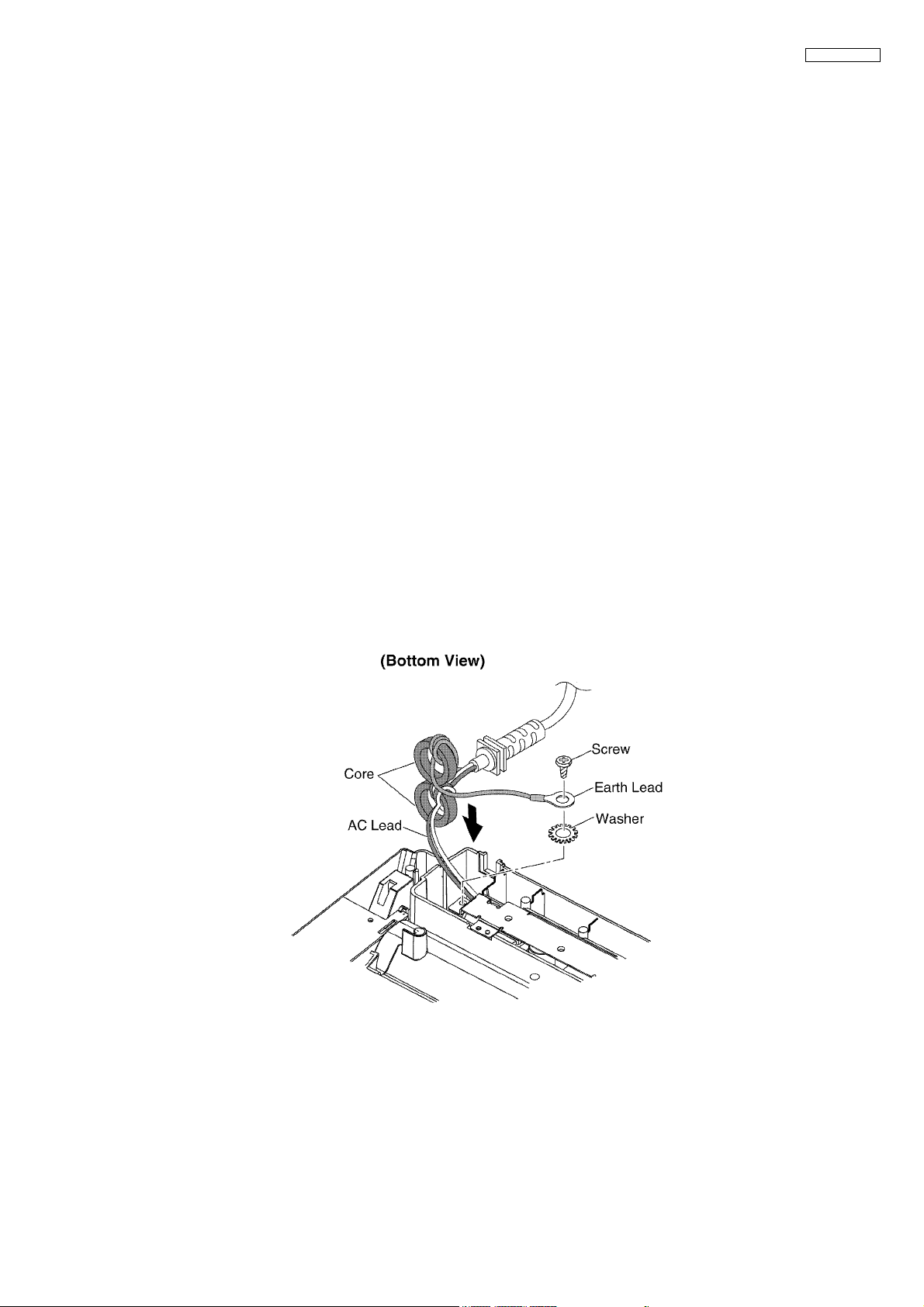
1.2. AC Caution
For safety, before closing the lower cabinet, please make sure of the following precautions.
1. The earth lead is fixed with the screw.
2. The AC lead is connected properly to power supply board.
3. Wrap the earth lead around the core 3 times.
4. Wrap the AC lead around the core 2 times.
3
KX-FP701LA
1.3. Personal Safety Precautions
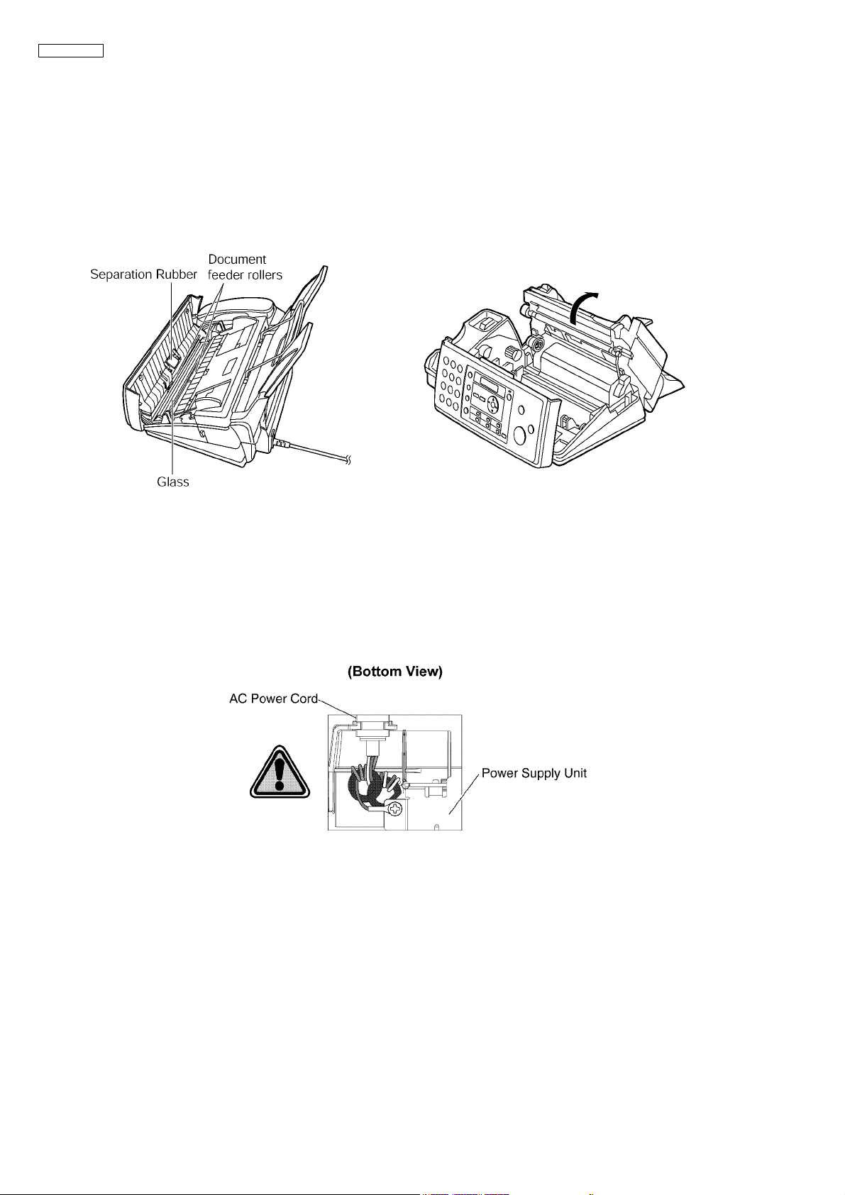
1.3.1. Moving Sections of the Unit
Be careful not to let your hair, clothes, fingers, accessories, etc., become caught in any moving sections of the unit.
The moving sections of the unit are the rollers and a gear. There is a separation roller and a document feed roller which are
rotated by the document feed motor. A gear rotates the two rollers. Be careful not to touch them with your hands, especially
when the unit is operating.
1.3.2. Live Electrical Sections
All the electrical sections of the unit supplied with AC power by the AC power cord are live.
Never disassemble the unit for service with the AC power supply plugged in.
CAUTION:
AC voltage is supplied to the primary side of the power supply unit. Therefore, always unplug the AC power cord before disassembling for service.
4
KX-FP701LA
1.4. Service Precautions
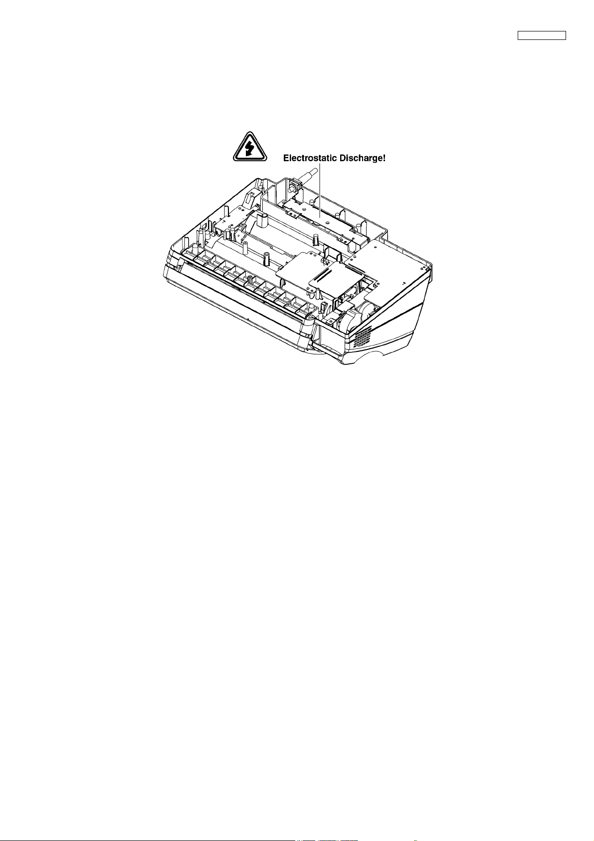
1.4.1. Precautions to Prevent Damage from static Electricity
Electrical charges accumulate on a person. For instance, clothes rubbing together can damage electric elements or change their
electrical characteristics. In order to prevent static electricity, touch a metallic part that is grounded to release the static electricity.
Never touch the electrical sections such as the power supply unit, etc.
5
KX-FP701LA
2Warning
2.1. About Lead Free Solder (PbF: Pb free)
Note:
In the information below, Pb, the symbol for lead in the periodic table of elements, will refer to standard solder or solder that contains lead.
We will use PbF solder when discussing the lead free solder used in our manufacturing process which is made from Tin, (Sn),
Silver, (Ag), and Copper, (Cu).
This model, and others like it, manufactured using lead free solder will have PbF stamped on the PCB. For service and repair
work we suggest using the same type of solder.
Caution
• PbF solder has a melting point that is 50° ~ 70° F, (3 0 ° ~ 40°C) higher than Pb solder. Please use a soldering iron with temperature control and adjust it to 700° ± 20° F, (370° ± 10°C).
• Exercise care while using higher temperature soldering irons.: Do not heat the PCB for too long time in order to prevent solder
splash or damage to the PCB.
• PbF solder will tend to splash if it is heated much higher than its melting point, approximately 1100°F, ( 60 0 °C).
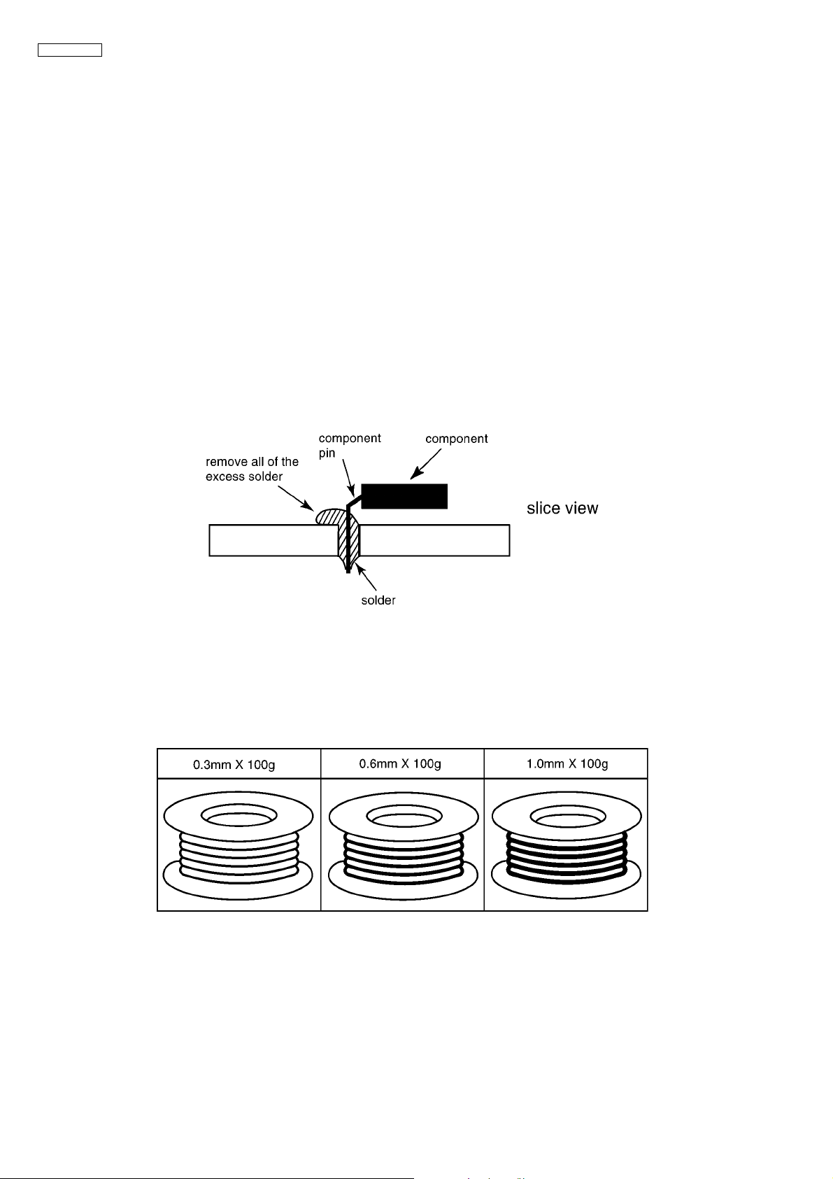
• When applying PbF solder to double layered boards, please check the component side for excess which may flow onto the
opposite side (See figure, below).
2.1.1. Suggested PbF Solder
There are several types of PbF solder available commercially. While this product is manufactured using Tin, Silver, and Copper,
(Sn+Ag+Cu), you can also use Tin and Copper, (Sn+Cu), or Tin, Zinc, and Bismuth, (Sn+Zn+Bi). Please check the manufacturer’s specific instructions for the melting points of their products and any precautions for using their product with other
materials.
The following lead free (PbF) solder wire sizes are recommended for service of this product: 0.3mm, 0.6mm and 1.0mm.
2.2. Discarding of P. C. Board
When discarding P. C. Board, delete all personal information such as telephone directory and caller list or scrap P. C. Board.
6
KX-FP701LA
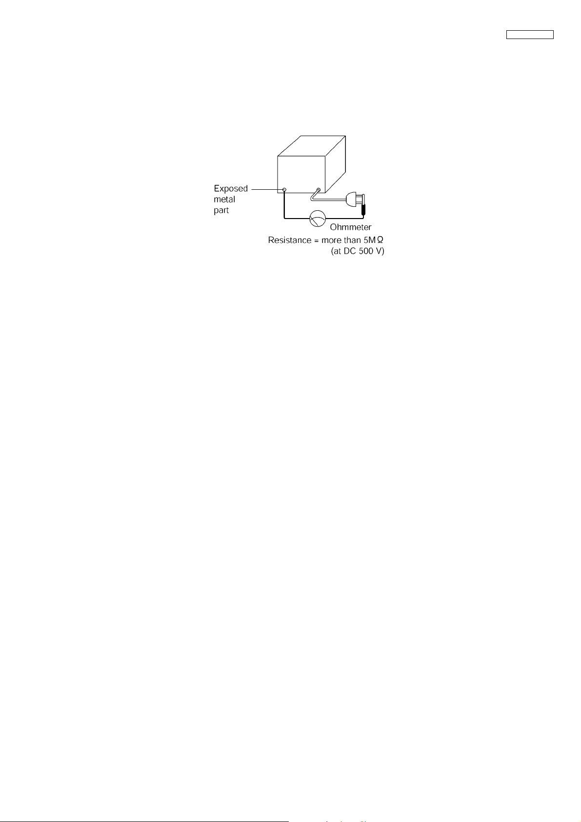
2.3. Insulation Resistance Test
1. Unplug the power cord and short the two prongs of the plug with a jumper wire.
2. Turn on the power switch.
3. Measure the resistance value with an ohmmeter between the jumpered AC plug and each exposed metal cabinet part
(screw heads, control shafts, bottom frame, etc.).
Note: Some exposed parts may be isolated from the chassis by design. These will read infinity.
4. If the measurement is outside the specified limits, there is a possibility of a shock hazard.
2.4. Battery Caution
Danger of explosion if battery is incorrectly replaced. Replace only with the same or equivalent type recommended by the manufacturer. Dispose of used batteries according to the manufacturer’s instruction.
CAUTION:
The lithium battery is a critical component (type No. CR2032). Please observe for the proper polarity and the exact location
when replacing it and soldering the replacement lithium battery in.
7

KX-FP701LA
3 Specifications
Any details given in these instructions are subject to change without notice.
Applicable Lines: Public Switched Telephone Network
Document Size: Max. 216 mm in width, Max. 600 mm in length
Effective Scanning Width: 208 mm
Recording Paper Size: Letter: 216 mm × 279 mm
Effective Printing Width: 208 mm
Recording Paper Weight:
60 g/m
2
to 90 g/m
Transmission Speed*1 : Approx. 12 s/page*
Scanning Density: Horizontal: 8 pels/mm
Ver tica l:
3.85 lines/mm (standard resolution)
7.7 lines/mm (fine/photo resolution)
15.4 lines/mm (super fine resolution)
Photo Resolution: 64 levels
Scanner Type: Contact Image Sensor
Printer Type: Thermal Transfer on plain paper
Data Compression System: Modified Huffman (MH), Modified READ (MR), Modified Modified READ (MMR)
Modem Speed: 9,600 / 7,200 / 4,800 / 2,400 bps; Automatic Fallback
Operating Environment: 5—35°C, 20—80 % RH (Relative Humidity)
Dimensions: Approx. height 185 mm × width 355 mm × depth 272 mm
Mass (Weight): Approx. 3.5 kg
Power Consumption: Standby: Approx. 1.5 W
Transmission: Approx. 12 W
Reception: Approx. 30 W (When receiving a 20% black document)
Copy: Approx. 40 W (When copying a 20% black document)
Maximum: Approx. 135 W (When copying a 100% black document)
Power Supply: 120 V AC, 60 Hz
Fax Memory Capacity*
3
:
Transmission: Approx. 25 pages
Reception: Approx. 28 pages
(Based on the ITU-T No. 1 Test Chart in standard resolution, without using the Error
Correction Mode.)
2
2
1
*
Transmission speed depends on the contents of the pages, resolution, telephone line conditions and capability of the other
party’s machine.
2
*
Transmission speed is based on the ITU-T No. 1 Test Chart with memory scanning original mode. If the capability of the other
party’s machine is inferior to your unit, the transmission time may be longer. (Refer to 16.3.1.ITU-T No.1 Test chart (P.166).)
3
*
If an error occurs during fax reception, such as a paper jam or if the recording paper runs out, the fax and subsequent faxes will
be retained in memory.
8
4 General/Introduction
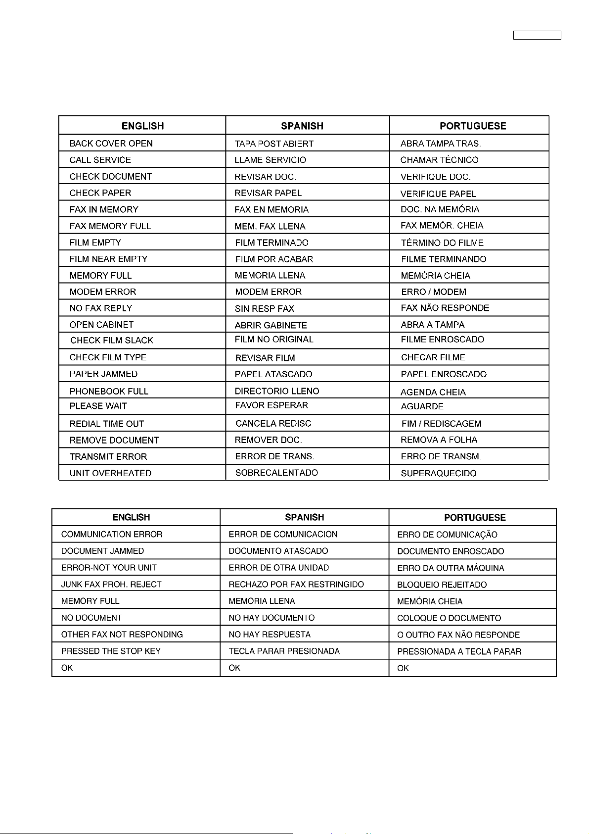
4.1. Error Message
4.1.1. Display
KX-FP701LA
4.1.2. Report
9
KX-FP701LA
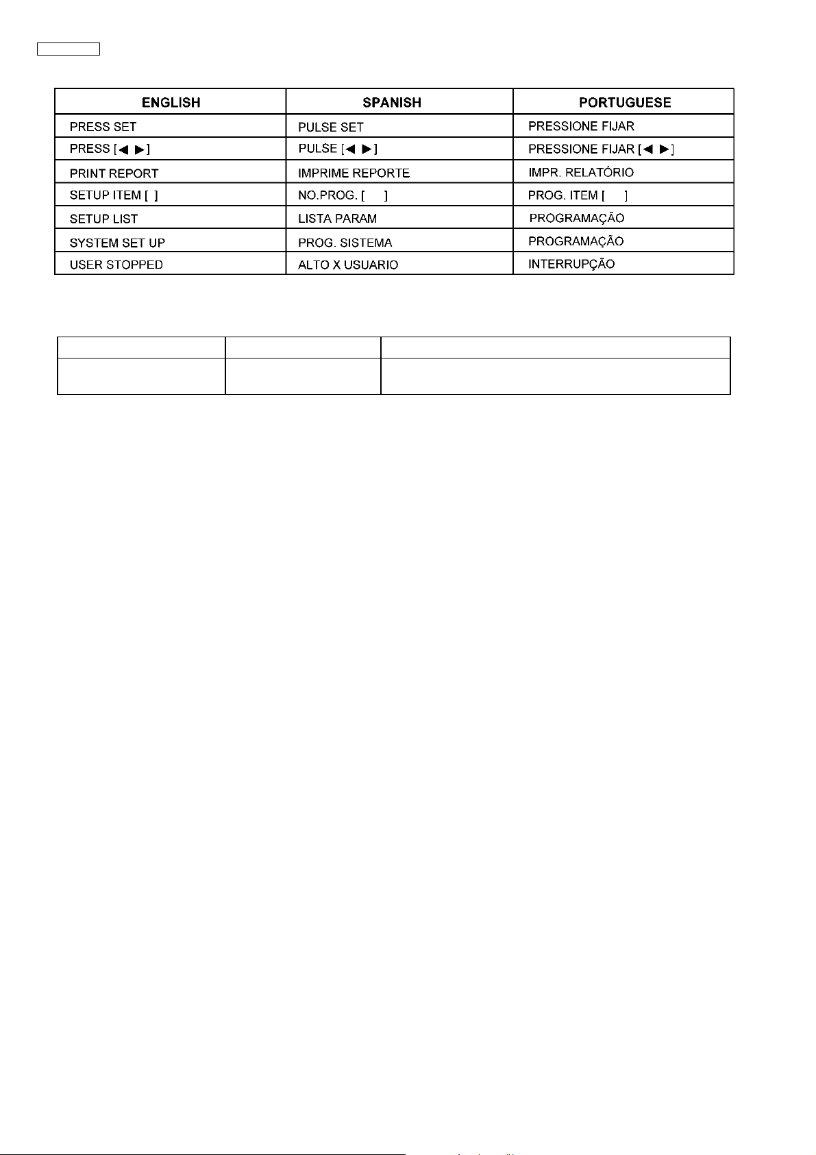
4.1.3. Other
4.2. Optional Accessories
Model No. Description Specification
KX-FA57A
*1
To ensure the unit operates properly, we recommend using the Panasonic replacement film.
The ink film is not reusable. Do not rewind and use the ink film again.
Replacement Film
*1
70 m × 1 rolls
(Prints about 225 Letter-sized pages)
5Features
General
• LCD (Liquid Crystal Display) readout
Plain Paper Facsimile Machine
• 12 second transmission speed*
• A4, Letter, G3 compatible
• Automatic document feeder (up to 10 sheets)
• Quick scan
• Resolution: Standard/Fine/Super fine/Photo (64 level)
• Broadcast
• 50-sheet recording paper capacity
• Automatic fax/phone switching
• Distinctive ring detection **
* The 12 second speed is based upon the ITU-T No. 1 Test
Chart on the condition that memory transmission is performed.
** Subscription to distinctive ring services is required.
Large Memory... Performed by DRAM
Approx. 28 pages of memory reception
Approx. 25 pages of memory transmission
Integrated Telephone System
• On-hook dialing
• Voice muting
• Redialing function
• 106-station telephone directory with Phonebook
• Caller ID service
This unit is compatible with the Caller ID service offered by
your local telephone company. To use this unit’s Caller ID
features, you must subscribe to Caller ID service.
Important:
- This unit will only display the caller’s telephone number
and name.
- This unit will not support future additional telephone services.
- Depending on the service of the local telephone company, the date/time of the call or the caller’s name may
not be displayed.
Make sure the following ring count is set to 2 or more rings
beforehand.
- FAX ring count (feature #06 on P.97)
- The name display service may not be available in some
areas. For further information, please contact your telephone company.
Enhanced Copier Function
• Multi-copy function (up to 50 copies)
• Enlargement and reduction
•Collate
• 64-Level halftone
10
6 Technical Descriptions
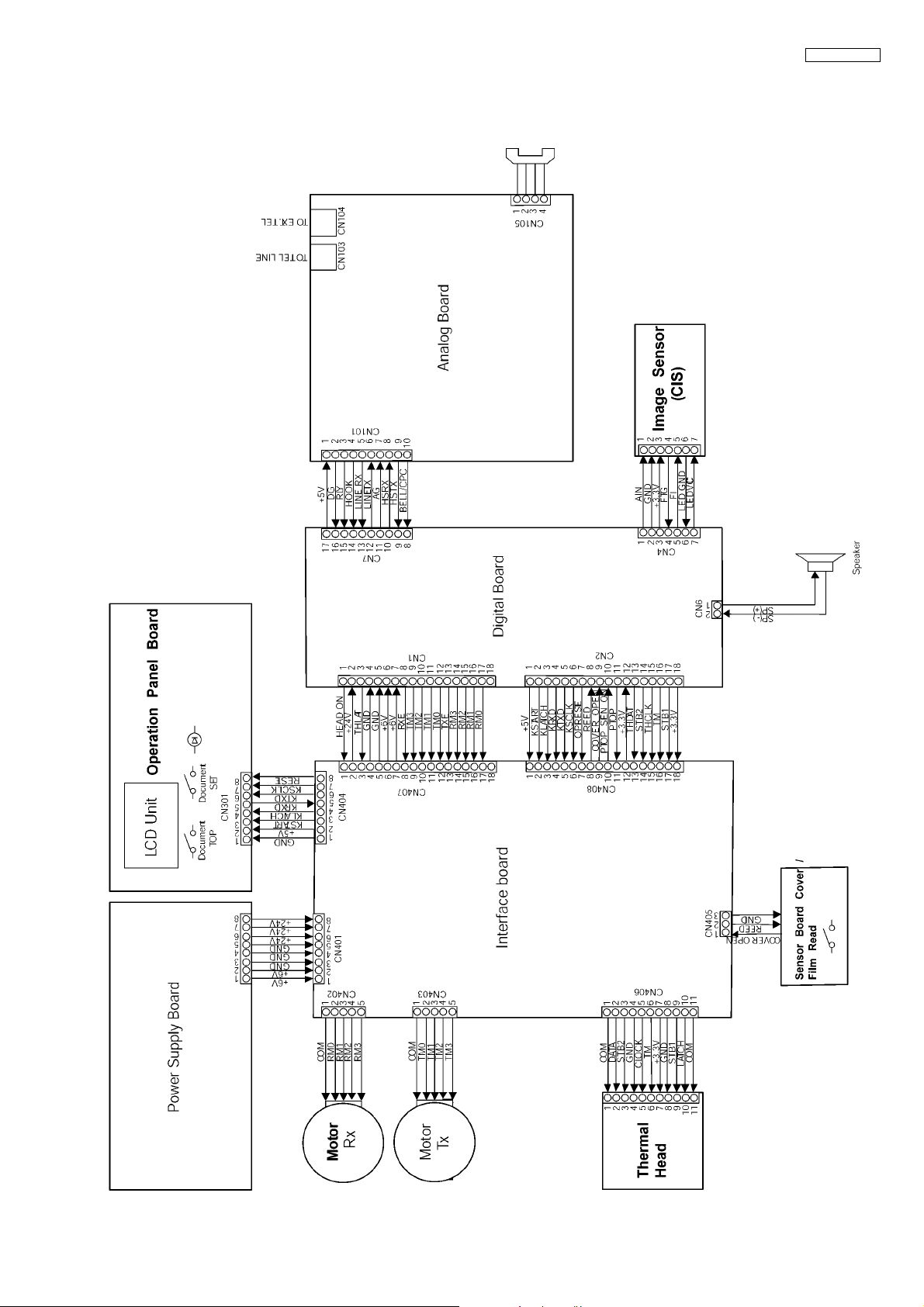
6.1. Connection Diagram
KX-FP701LA
11

KX-FP701LA
6.2. General Block Diagram
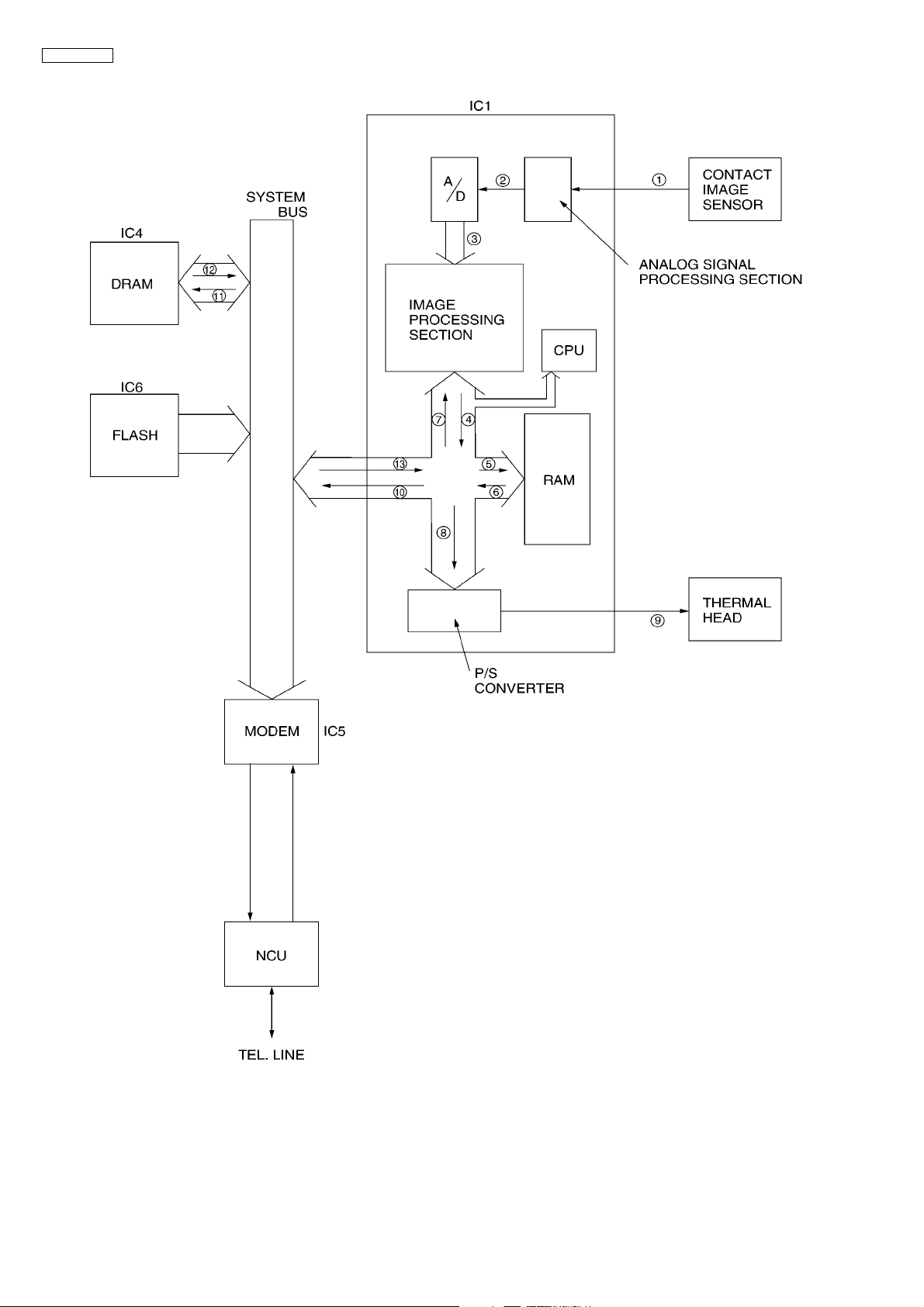
The following is an outline of each device IC on the digital board. (Refer to 6.2.1.General Block Diagram (P.13).).
1. ASIC (IC1)
Composed mainly of an address decoder and a modem control.
Controls the general FAX operations.
Controls the operation panel I/F.
Controls the thermal head I/F and CIS I/F.
Performs the image processing.
CPU and Real time clock
Provides the reset pulse for each of the major ICs.
2. Flash ROM (IC6)
Contains all of the program instructions on the unit operations.
This memory is used mainly for the parameter working in the storage area.
3. Dynamic RAM (IC4)
This memory is used mainly for the parameter working in the storage area.
4. MODEM (IC5)
Performs the modulation and the demodulation for FAX communication.
5. Read Section
“Contact Image Sensor “(CIS) to read transmitted documents.
6. Motor Driver (IC401,IC402)
Drives the transmission motor and the reception motor.
7. Thermal Head
Contains heat-emitting elements for dot matrix image printing.
8. Analogue Board
Composed of ITS circuit and NCU circuit.
9. Sensor Section
Composed of a cover open, a document set switch, a document top switch, a paper top sensor.
10. Power Supply Board Switching Section
Supplies +6V and +24V to the unit.
12
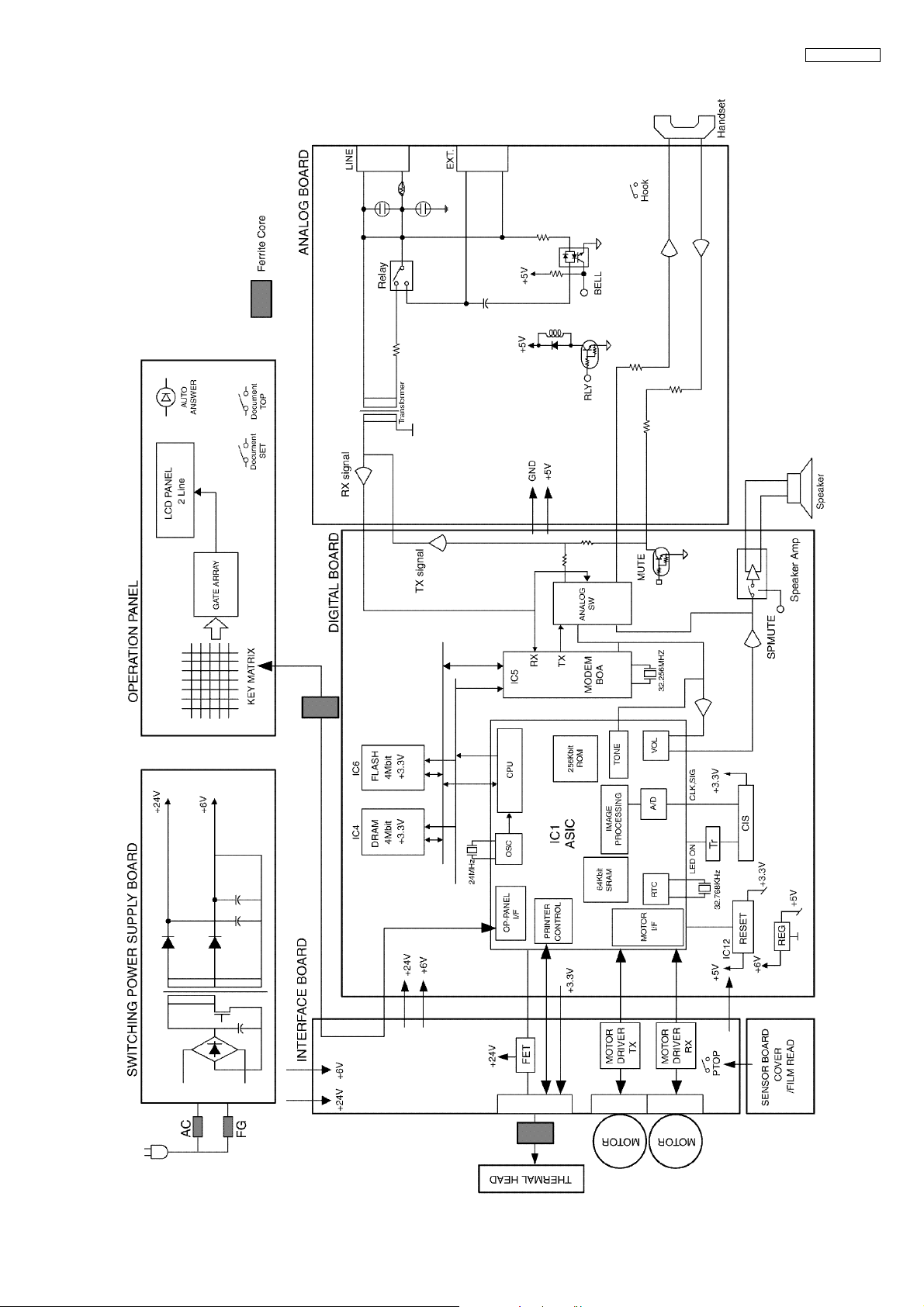
6.2.1. General Block Diagram
KX-FP701LA
13
KX-FP701LA
6.3. Control Section
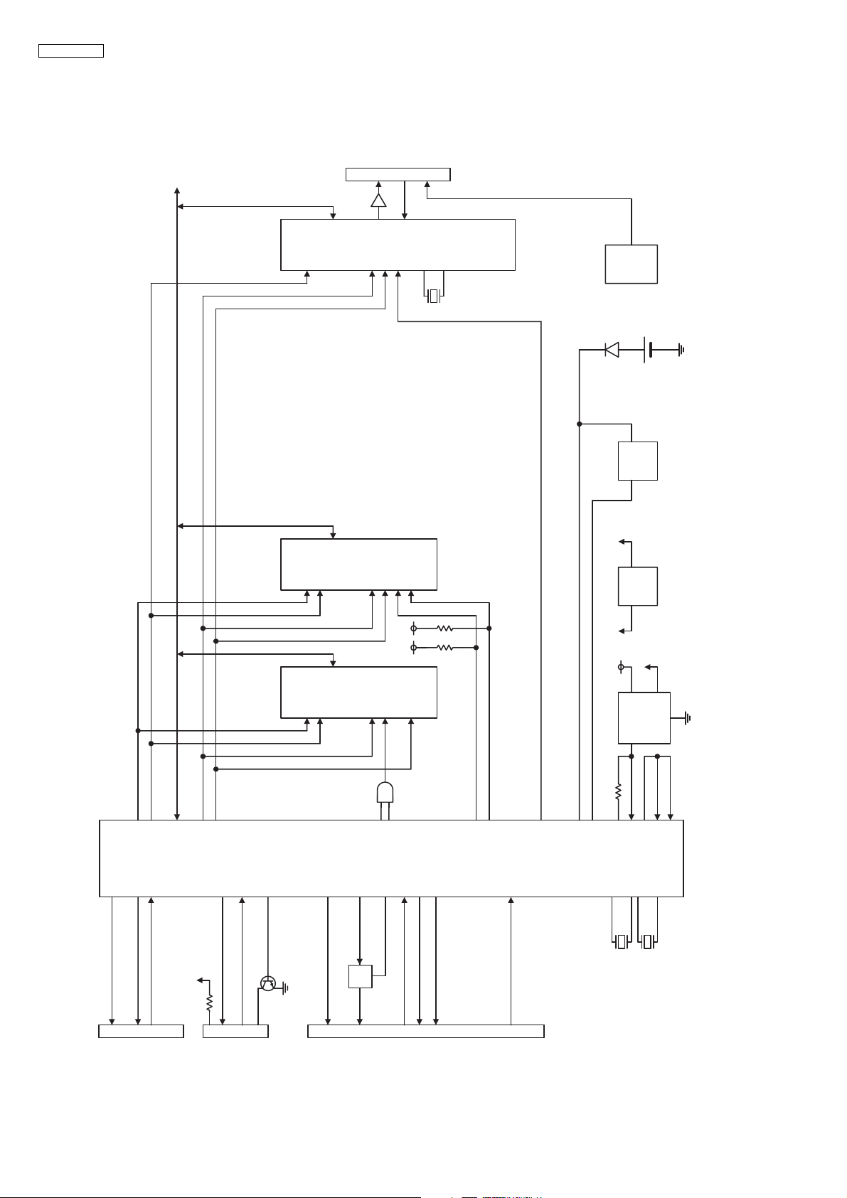
6.3.1. Block Diagram
IC5
MODEM
]
:0
TO
Analog
Board
CN7
TX
XRD
XWR
RX
XCS
IC13
SP-AMP
D[7:0]
A[4:0]
A
[4
]
]
IC4
:0
IC6
:0
]
[5
]
[5
:0
DRAM
B
A
R
:4
A
[7
FLASH
B
A
R
2
A
[1
A[9:0]
A[17:0]
D[7:0]
D[7:0]
XRD
XRD
XWR
XCS
XRAS
XCAS
+3.3V
XWR
32.256MHz
BATT
+
-
+3.3V/BATT
KX-FP701LA : CONTROL SECTION BLOCK DIAGRAM
Q7
+3.3V+2.5V
+2.5V/BATT
Q5
+5V
+3.3V
IN
OUT
IC3
RESET-IC
GND
VDET
IC1
ASIC
OP-RESET
CN2 to CN404
RBA[5:0]
ADR[12:0]
ADR[15:13]
KSTART,KLATCH
KSCLK,KTXD
KRXD
TO
Operation
Board
DB[7:0]
+5V
CN4
XRD
XWR
F1,FTG
TO
VIDEO
CIS
CISLEDON
THLAT,THC,THDAT
CN1,2
Q2,4,14
STB1,STB2
IC7
AND
HEADON
XROMCS
XOPRBE
RXE
TM
14
RXE,RM0~3
TXE,TM0~3
XRAS
XCAS
REED,PTOP,COVER OPEN
XMDMCS
XRESET
XRESETI
XWDERR
XORESET
+3.3V/BATT
+2.5V/BATT
XBACKEN
24MHz
32.768KHz
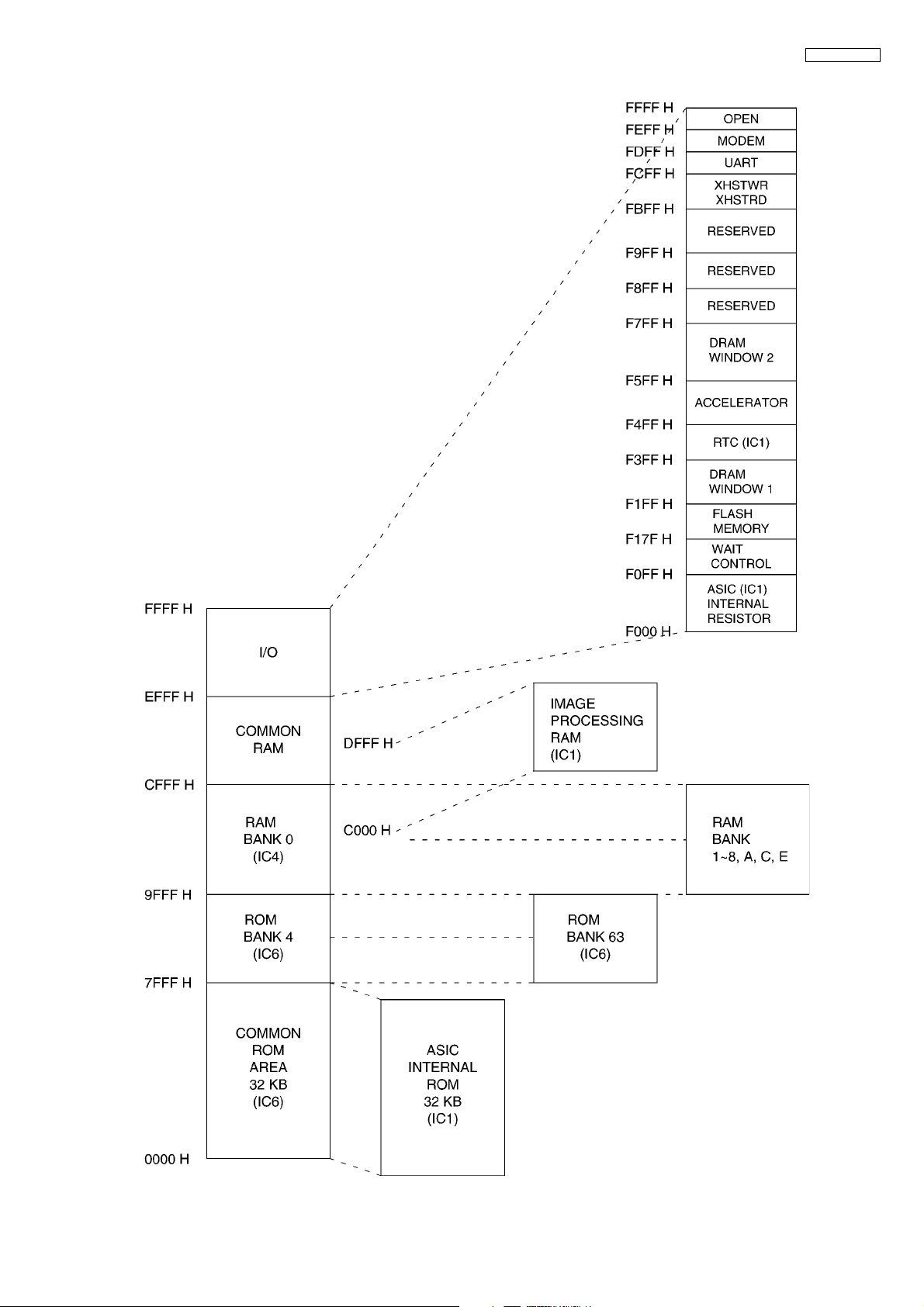
6.3.2. Memory Map
KX-FP701LA
15
KX-FP701LA
6.3.3. ASIC (IC1)
This custom IC is used for the general FAX operations.
1. CPU:
This model uses a Z80 equivalent to the CPU operating
at 12 MHz. Most of the peripheral functions are performed
by custom-designed LSIs. Therefore, the CPU only works
for processing the results.
2. RTC:
Real Time Clock
3. DECODER:
Decodes the address.
4. ROM/RAM I/F:
Controls the SELECT signal of ROM or RAM and the
bank switching.
5. CIS I/F:
Controls the document reading.
6. IMAGE DATA RAM:
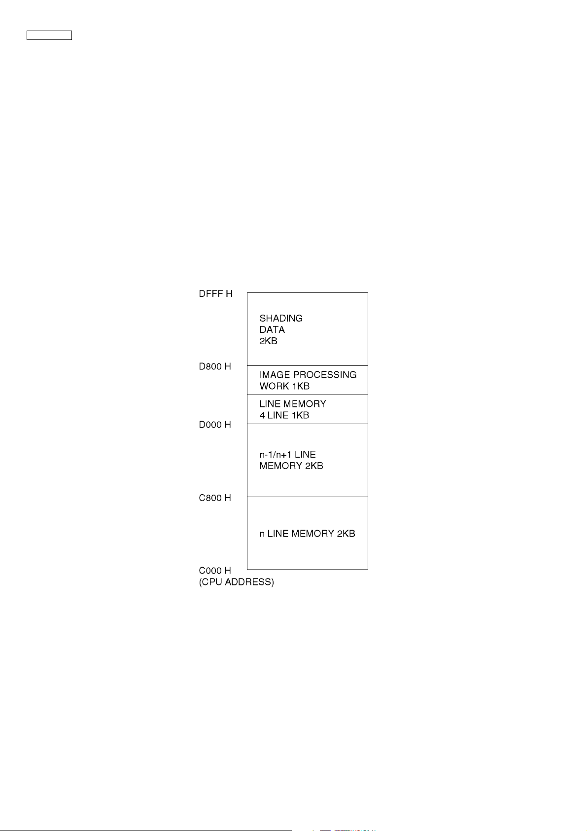
This memory is programmed into the ASIC and uses 8
KB for the image processing. (See Fig. A.*)
7. THERMAL HEAD I/F:
Transmits the recorded data to the thermal head.
8. MOTOR I/F:
Controls the transmission motor which feeds the document.
Controls the receiving motor which feeds the recording
paper.
9. OPERATION PANEL I/F:
Serial interface with Operation Panel.
10. I/O PORT:
I/O Port Interface.
11. ANALOGUE UNIT:
Electronic volume for the monitor.
Sends beep tones, etc.
Fig. A
Note:
This memory is incorporated into the ASIC (IC1) and used for the image processing.
Fig. A shows the memory map of the Image Data RAM.
16
Descriptions of Pin Distribution (IC1)
KX-FP701LA
NO. SIGNAL I/O POWER SUPPLIED
VOLTAGE
1 VSSA GND POWER SOURCE (ANALOG GND)
2 VDDA 3.3 3.3V POWER SOURCE (ANALOG +3.3V)
3 AIN1 A 3.3V CIS IMAGE SIGNAL INPUT (SIG)
4 AIN2 A 3.3V THERMISTOR TEMPERATURE WATCH INPUT
5 AIN3 A 3.3V LINE VOLTAGE DETECTION SIGNAL INPUT (DCIN)
6 AMON A 3.3V ANALOG SIGNAL MONITOR TERMINAL
7 VSS GND POWER SOURCE (GND)
8 X32OUT O 3.3V/BATT RTC (32.768KHz) CONNECTION
9 X32IN I 3.3V/BATT RTC (32.768KHz) CONNECTION
10 VDD (3.3V / B) ----- POWER SOURCE (+3.3V/LITHIUM BATTERY)
11 XBACEN I 3.3V/BATT BACKUP ENABLE
12 XRAMCS O 3.3V/BATT NOT USED
13 VDD (3.3V / B) ----- POWER SOURCE(+3.3V / LITHIUM BATTERY)
14 VDD (2.5V/B) ----- POWER SOURCE (+2.5V / LITHIUM BATTERY)
15 FTG O 3.3V START SIGNAL OUTPUT FOR CIS (SI)
16 F1 O 3.3V CLOCK SIGNAL OUTPUT FOR CIS (CLK)
17 F2/OP O 3.3V OUTPUT PORT (THON)
18 FR/OP O 3.3V OUTPUT PORT (MDMRST)
19 CPC I 3.3V INPUT PORT (BELL/CPC)
20 RVN I 3.3V INPUT PORT (REED)
21 IRDATXD/IOP O 3.3V OUTPUT PORT (NOT USED)
22 IRDARXD/IOP80 O 3.3V OUTPUT PORT (NOT USED)
23 TXD/IOP O 3.3V OUTPUT PORT (FILMEND)
24 RXD/IOP O 3.3V OUTPUT PORT (NOT USED)
25 XRTS/IOP O 3.3V OUTPUT PORT (NOT USED)
26 XCTS/IOP O 3.3V OUTPUT PORT (NOT USED)
27 VDD (2.5V) ----- POWER SOURCE (+2.5V)
28 TONE1 A 3.3V TONE OUTPUT
29 TONE2 A 3.3V TONE OUTPUT
30 VOLUREF A 3.3V ANALOG REF VOLTAGE
31 VOLUOUT A 3.3V VOLUME OUTPUT
32 VOLUIN A 3.3V VOLUME INPUT
33 XNMI I 3.3V HIGH FIXED
34 FMEMDO/IOP O 3.3V OUTPUT PORT (CISLED)
35 VDD (3.3V) ----- POWER SOURCE (+3.3V)
36 VSS GND POWER SOURCE (GND)
37 VSS GND POWER SOURCE (GND)
38 VDD (3.3V) ----- POWER SOURCE (+3.3V)
39 MIDAT/IOP O 3.3V OUTPUT PORT (TONE1EN)
40 MICLK/IOP O 3.3V OUTPUT PORT (HSTX MUTE)
41 MILAT/IOP O 3.3V OUTPUT PORT (HS RX EN)
42 20KOSC/IOP O 3.3V OUTPUT PORT (CIS ON)
43 XWAIT I 3.3V INPUT PORT (HOOK)
44 HSTRD/IOP O 3.3V OUTPUT PORT (RLY)
45 HSTWR/IOP O 3.3V OUTPUT PORT (NOT USED)
46 XOPRBE O 3.3V MFCS
47 ADR15 O 3.3V CPU ADDRESS BUS 15 (NOT USED)
48 ADR14 O 3.3V CPU ADDRESS BUS 14 (NOT USED)
49 ADR13 O 3.3V CPU ADDRESS BUS 13 (NOT USED)
50 VDD (2.5V) ----- POWER SOURCE (+2.5V)
51 XOUT O 3.3V SYSTEM CLOCK (24MHz)
52 XIN I 3.3V SYSTEM CLOCK (24MHz)
53 VSS GND POWER SOURCE (GND)
54 VDD (3.3V) ----- POWER SOURCE (+3.3V)
55 XTEST O 3.3V 24MHz CLOCK
56 TEST1 I 3.3V HIGH FIXED
DESCRIPTION
17

KX-FP701LA
NO. SIGNAL I/O POWER SUPPLIED
DESCRIPTION
VOLTAGE
57 TEST2 I 3.3V HIGH FIXED
58 TEST3 I 3.3V HIGH FIXED
59 TEST4 I 3.3V HIGH FIXED
60 XMDMINT I 3.3V MODEM INTERRUPT
61 XMDMCS O 3.3V MODEM CHIP SELECT
62 XRAS/IOP O 3.3V DRAM (IC4) ROW ADDRESS STROBE
63 XCAS1/IOP O 3.3V DRAM (IC4) CULUMN ADDRESS STROBE
64 XCAS2/IOP O 3.3V OUTPUT PORT (NOT USED)
65 XRESCS2 O 3.3V FLASH CHIP SELECT (XRESCS2)
66 DB3 I/O 3.3V CPU DATA BUS 3
67 DB2 I/O 3.3V CPU DATA BUS 2
68 DB4 I/O 3.3V CPU DATA BUS 4
69 DB1 I/O 3.3V CPU DATA BUS 1
70 DB5 I/O 3.3V CPU DATA BUS 5
71 VDD (3.3V) ----- POWER SOURCE (+3.3V)
72 VSS GND POWER SOURCE (GND)
73 VSS GND POWER SOURCE (GND)
74 VDD (3.3V) ----- POWER SOURCE (+3.3V)
75 DB0 I/O 3.3V CPU DATA BUS 0
76 DB6 I/O 3.3V CPU DATA BUS 6
77 DB7 I/O 3.3V CPU DATA BUS 7
78 XROMCS O 3.3V ROM (IC6) CHIP SELECT
79 RD O 3.3V CPU RD
80 WR O 3.3V CPU WR
81 ADR0 O 3.3V CPU ADDRESS BUS 0
82 ADR1 O 3.3V CPU ADDRESS BUS 1
83 ADR2 O 3.3V CPU ADDRESS BUS 2
84 ADR3 O 3.3V CPU ADDRESS BUS 3
85 ADR4 O 3.3V CPU ADDRESS BUS 4
86 ADR5 O 3.3V CPU ADDRESS BUS 5
87 VSS GND POWER SOURCE (GND)
88 VDD (2.5V) ----- POWER SOURCE (+2.5V)
89 ADR6 O 3.3V CPU ADDRESS BUS 6
90 ADR7 O 3.3V CPU ADDRESS BUS 7
91 ADR8 O 3.3V CPU ADDRESS BUS 8
92 ADR9 O 3.3V CPU ADDRESS 9
93 ADR10 O 3.3V CPU ADDRESS 10
94 ADR11 O 3.3V CPU ADDRESS 11
95 ADR12 O 3.3V CPU ADDRESS 12
96 RBA0 O 3.3V ROM/RAM BANK ADDRESS 0
97 RBA1 O 3.3V ROM/RAM BANK ADDRESS 1
98 RBA2 O 3.3V ROM/RAM BANK ADDRESS 2
99 RBA3 O 3.3V ROM/RAM BANK ADDRESS 3
100 RBA4 O 3.3V ROM/RAM BANK ADDRESS 4
101 RBA5 O 3.3V ROM/RAM BANK ADDRESS 5
102 RBA6/IOP96 O 3.3V OUTPUT PORT (PTOP SEN ON)
103 STB1 O 3.3V STROBE SIGNAL OUTPUT TO THERMAL HEAD
104 STB2 O 3.3V STROBE SIGNAL OUTPUT TO THERMAL HEAD
105 STB3 O 3.3V (NOT USED)
106 XRESET I 3.3V RESET INPUT
107 VDD (3.3V) ----- POWER SOURCE (+3.3V)
108 VSS GND POWER SOURCE (GND)
109 VSS GND POWER SOURCE (GND)
110 VDD (3.3V) ----- POWER SOURCE (+3.3V)
111 XORESET O 3.3V SYSTEM RESET OUTPUT
112 VDD(5V) ----- POWER SOURCE (+5V)
113 VSS GND POWER SOURCE (GND)
18

KX-FP701LA
NO. SIGNAL I/O POWER SUPPLIED
VOLTAGE
114 XRESETI I 3.3V RESET INPUT
115 WDERR O 3.3V WATCHED ERROR OUTPUT SIGNAL
116 THDAT O 3.3V RECORDED IMAGE OUTPUT (XTHDAT)
117 THCLK O 3.3V CLOCK OUTPUT FOR DATA TRANSFER (XTHCLK)
118 THLAT O 3.3V PULSE OUTPUT FOR DATA LATCH (XTHLAT)
119 STBNP I 0V INPUT PORT (NOT USED)
120 RM0/IOP O 3.3V RX MOTOR A PHASE
121 RM1/IOP I/O 3.3V RX MOTOR B PHASE
122 RM2/IOP I/O 3.3V RX MOTOR /A PHASE
123 RM3/IOP I/O 3.3V RX MOTOR /B PHASE
124 RXE/IOP O 3.3V RX MOTOR ENABLE
125 TMO O 3.3V TX MOTOR A PHASE
126 VDD (2.5V) ----- POWER SOURCE (+2.5V)
127 VSS GND POWER SOURCE (GND)
128 TM1/IOP O 3.3V TX MOTOR B PHASE
129 TM2/IOP O 3.3V TX MOTOR /A PHASE
130 TM3/IOP O 3.3V TX MOTOR /B PHASE
131 TXE/IOP O 3.3V TX MOTOR ENABLE
132 KSTART O 3.3V OPERATION PANEL CONTROL
133 KLATCH O 3.3V OPERATION PANEL CONTROL
134 KSCLK O 3.3V OPERATION PANEL CONTROL
135 KTXD O 3.3V OPERATION PANEL CONTROL
136 KRXD I 3.3V OPERATION PANEL CONTROL
137 FMEMCLK/IOP O 3.3V OUTPUT PORT (OP RESET)
138 FMEMDI/IOP O 3.3V OUTPUT PORT (SP MUTE)
139 ADSEL1 O 3.3V CHANNEL SELECT SIGNAL FOR AIN2
140 VDDA (2.5V) 2.5V POWER SOURCE (ANALOG +2.5V)
141 VREFB A 3.3V A/D CONVERTER'S ZERO STANDARD VOLTAGE
OUTPUT
142 VCL A 3.3V ANALOG PART STANDARD VOLTAGE SIGNAL
143 VREFT A 3.3V A/D CONVERTER'S FULL SCALE VOLTAGE OUTPUT
144 VSSA GND POWER SOURCE (ANALOG GND)
DESCRIPTION
6.3.4. Flash Memory (IC6)
This 512KB ROM (FLASH MEMORY) carries a common area of 32KB and bank areas which each have 8KB (BK4~BK63). The
addresses from 0000H to 7FFFH are for the common area and from 8000H to 9FFFH are for the bank areas.
6.3.5. Dynamic RAM (IC4)
The DRAM serves as CPU and receives memory.
The address is F200H~F3FFH (DRAM access window 1) and F600H~F7FFH (DRAM access window 2).
19
KX-FP701LA
6.3.6. Reset Circuit (Watch dog timer)
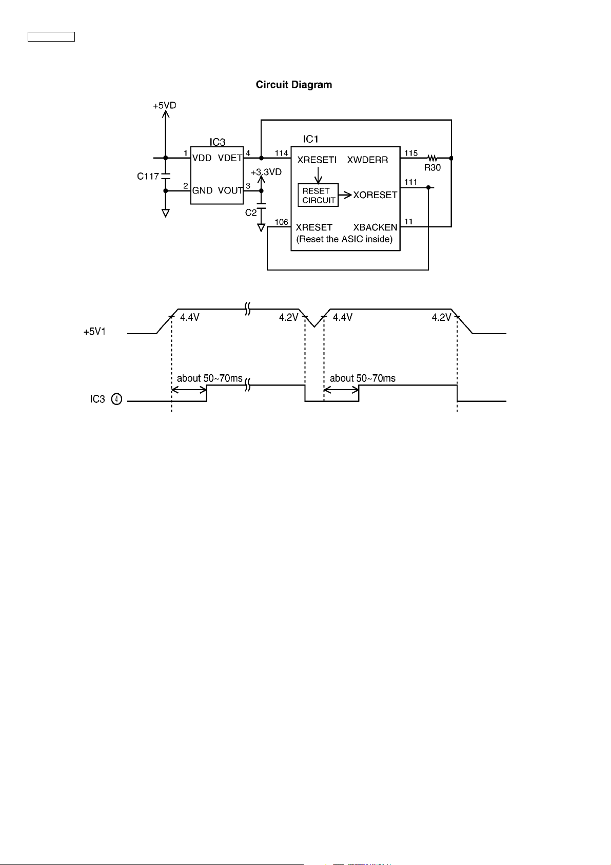
The output signal (reset) from pin 4 of the voltage detect IC (IC3) is input to the ASIC (IC1) 114 pin.
1. During a momentary power interruption, a positive reset pulse of 50~70 msec is generated and the system is reset completely.
2. The watch dog timer, built-in the ASIC (IC1), is initialized by the CPU about every 1.5 ms.
When a watch dog error occurs, pin 115 of the ASIC (IC1) becomes low level.
The terminal of the 'WDERR' signal is connected to the reset line, so the 'WDERR' signal works as the reset signal.
20
6.3.7. RTC Backup Circuit
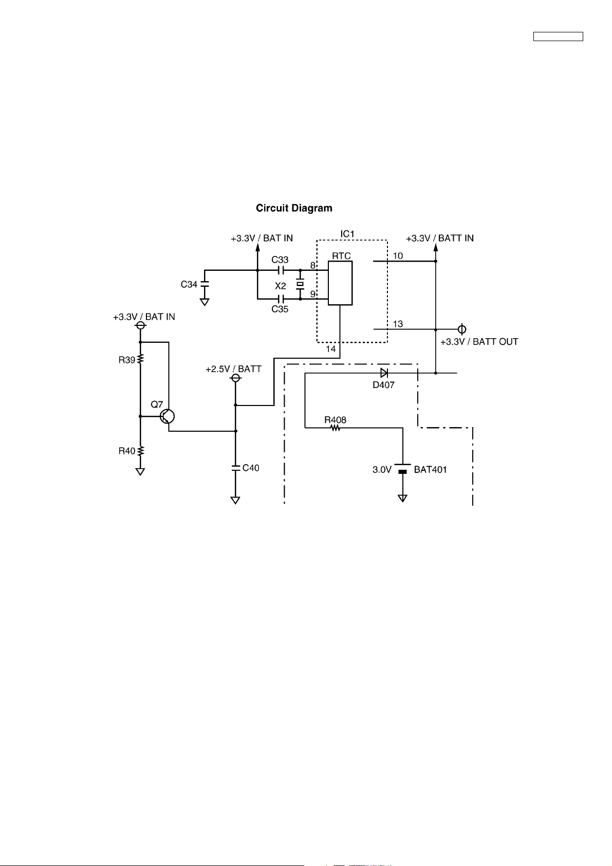
1. Function
This unit has a lithium battery (BAT401) which works for Real Time Clock IC (RTC: inside IC1).
The RTC continues to work, backed up by a lithium battery even when the power switch is OFF.
The user parameters for autodial numbers, the system setup data and others are in the FLASH MEMORY (IC6).
2. RTC Inside (IC1) Backup Circuit Operation
When the power switch is turned ON, power is supplied through Q7 to the RTC (inside IC1). At this time, the voltage at pin 14
of the IC1 is +2.5V. When the power switch is turned OFF, the BAT401 supplies power to RTC through D407 and Q505. The
voltage at pin 14 of IC1 is about +2.2V. When the power switch is OFF and the voltage of +3.3V decreases, pin 14 of RTC
(IC1) becomes roughly the same voltage as the battery voltage. RTC goes into the backup mode, in which the power consumption is lower.
KX-FP701LA
21
KX-FP701LA
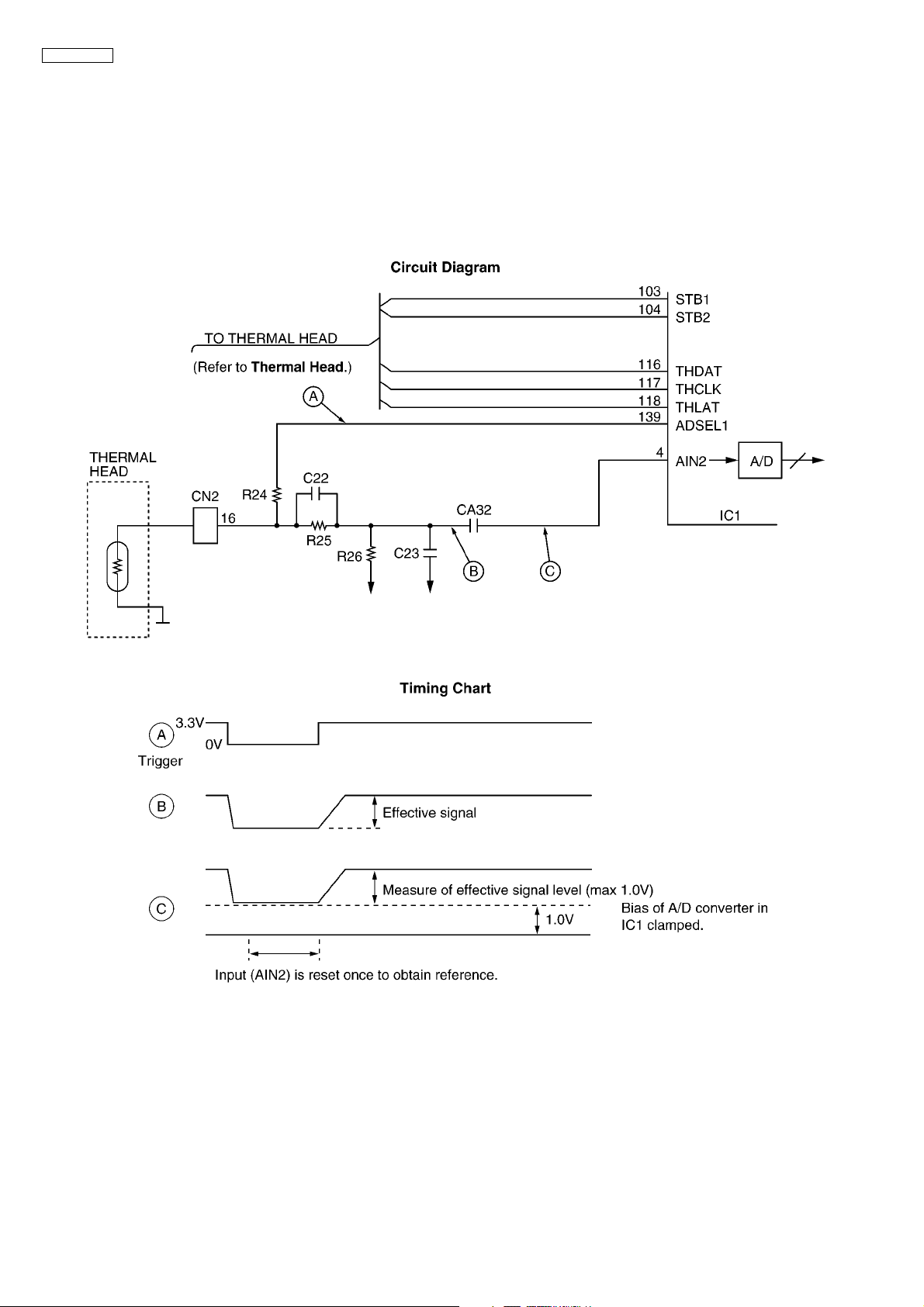
6.3.8. Supervision Circuit for the Thermal Head Temperature
1. Function
The thermistor changes the resistor according to the temperature and uses the thermistor's characteristics. The output of pin
139 of IC1 becomes a low level. Then when it becomes a high level, it triggers point A In point C, according to the voltage output time, the thermal head's temperature is detected.
After the thermal head temperature is converted to voltage in B, it is then changed to digital data in the A/D converter inside
IC1. The CPU decides the strobe width of the thermal head according to this value. Therefore, this circuit can keep the thermal head at an even temperature in order to stabilize the printing density and prevent the head from being overheated.
REFERENCE:
6.4.3.Thermal Head (P.25)
22

KX-FP701LA
6.4. Facsimile Section
6.4.1. Image Data Flow During Facsimile Operation
Copy (Fine, Super-Fine, Half Tone)
1. Line information is read by Contact Image Sensor (to be used as the reference white level) via route1, and is input to IC1.
Refer to 6.4.2.Block Diagram (P.24)
2. In IC1, the data is adjusted to a suitable level for A/D conversion in the Analogue Signal Processing Section, and via route2 it
is input to A/D conversion (8 bit). After finishing A/D conversion, the data is input to the Image Processing Section via route3.
Then via route4 and route5, it is stored in RAM as shading data.
3. The draft’s information that is read by CIS is input to IC1 via route1. After it is adjusted to a suitable level for A/D conversion
via route2, the draft’s information is converted to A/D (8 bit), and it is input to the Image Processing Section. The other side,
the shading data which flows from RAM via route6 and route7, is input to the Image Processing Section. After finishing the
draft’s information image processing, white is regarded as "0" and black is regarded as "1". Then via routes4 and 5, they are
stored in RAM.
4. The white/black data stored as above via routes6 and8 is input to the P/S converter. The white/black data converted to serial
data in the P/S converter is input to the Thermal Head via route9 and is printed out on recording paper.
Note:
Standard: Reads 3.85 times/mm
Fine: Reads 7.7 times/mm
Super-Fine: Reads 15.4 times/mm
Transmission
1. Same processing as Copy items 1 - 3.
2. The data stored in the RAM of IC1 is output from IC1 via routes6 and 10, and is stored in the system bus.
Via route11, it is stored in the communication buffer inside DRAM (IC4).
3. While retrieving data stored in the communication buffer synchronous with the modem, the CPU (inside IC1) inputs the data to
the modem along route12, where it is converted to serial analogue data and forwarded over the telephone lines via the NCU
Section.
Reception
1. The serial analogue image data is received over the telephone lines and input to the modem via the NCU section, where it is
demodulated to parallel digital data. Then the CPU (IC1) stores the data in the communication buffer DRAM (IC4) along
route12.
2. The data stored in DRAM (IC4) is decoded by the CPU (IC1) via route12, and is stored in DRAM (IC4) via routes13 and 5.
3. Same processing as Copy item 4.
23
KX-FP701LA
6.4.2. Block Diagram
24
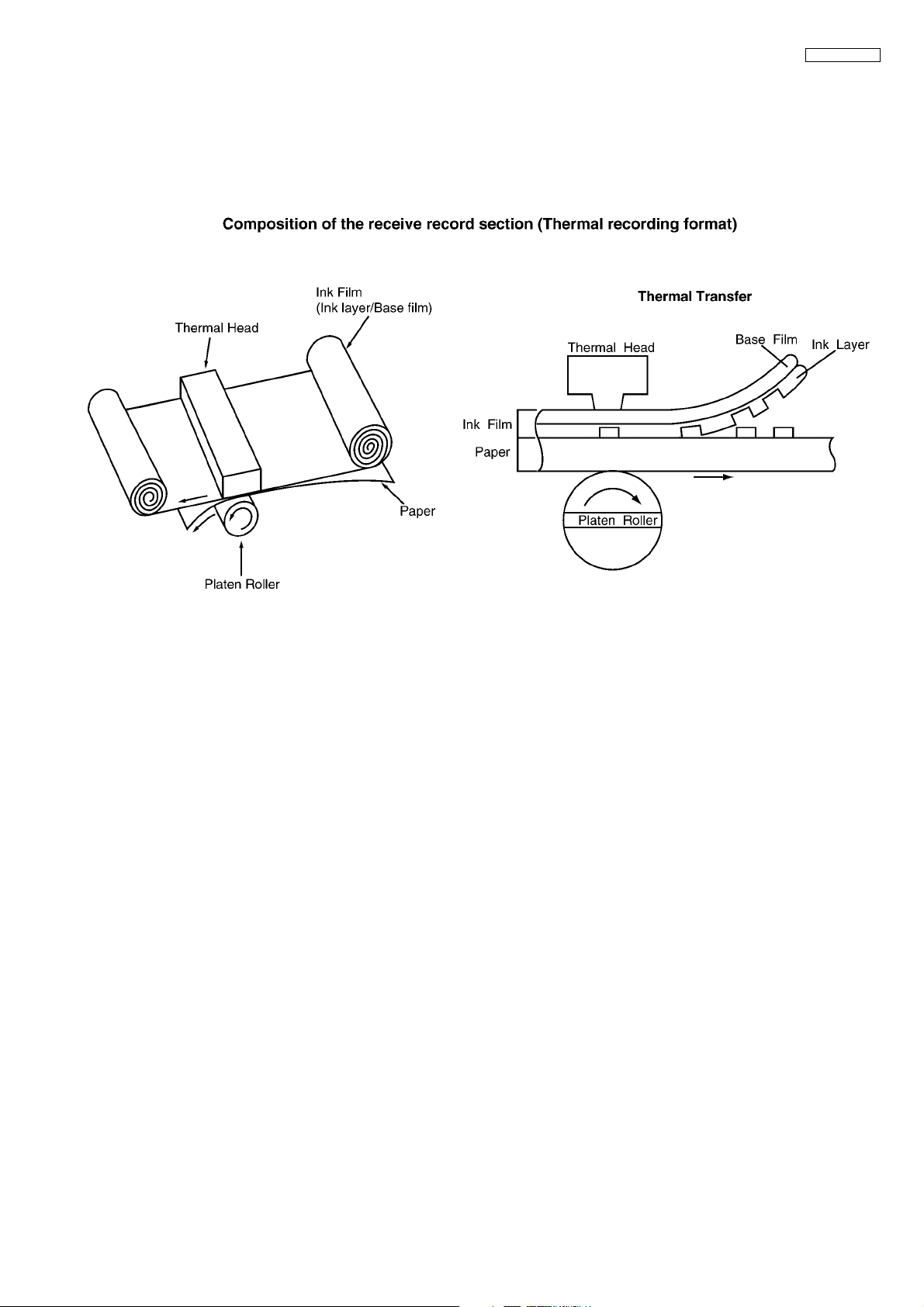
6.4.3. Thermal Head
1. Function
This unit utilizes the state of the art thermal printer technology.
The ink film is chemically processed. The ink film is comprised of two parts: an ink layer and a base film. When the thermalhead contacts this ink film, it emits heat momentarily, and the ink layer is melted and transferred to the paper. If this continues,
letters and/or diagrams appear, and the original document is reproduced.
KX-FP701LA
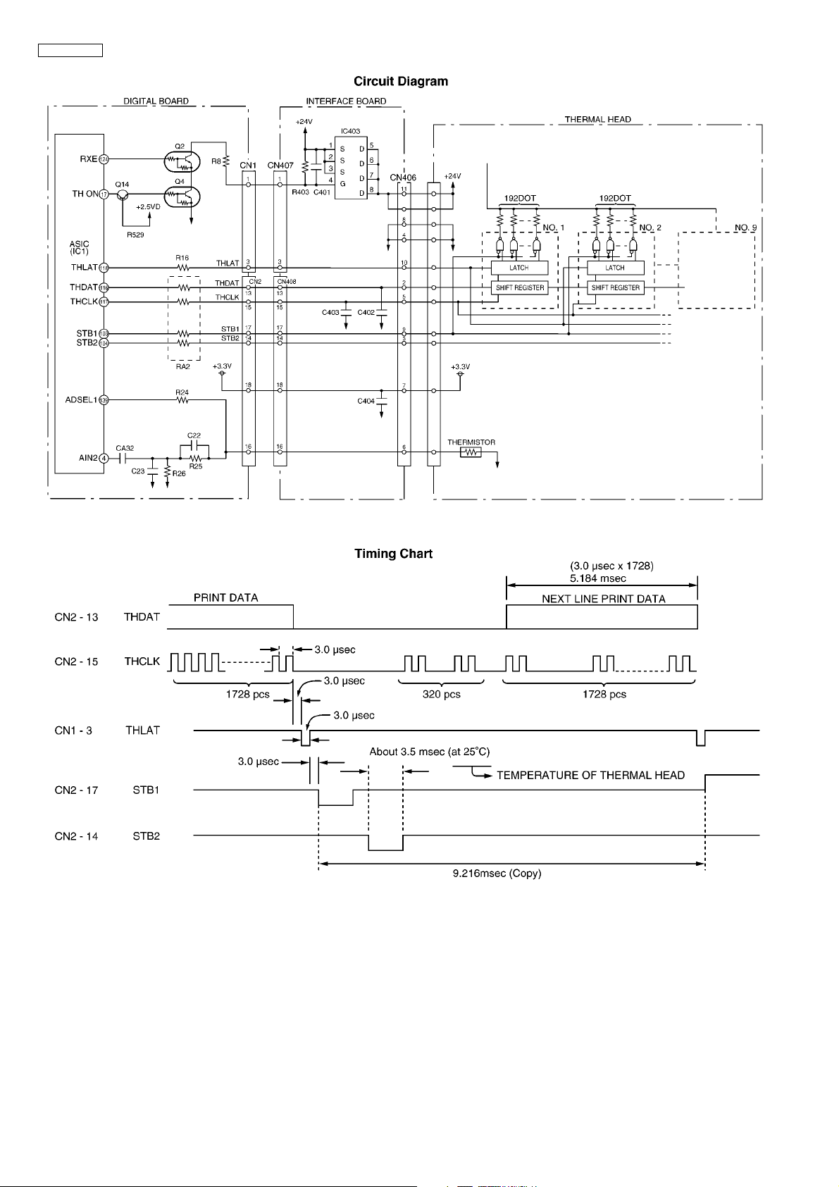
2. Circuit Operation
Refer to the block diagram and the timing chart on the following page.
There are 9 driver ICs aligned horizontally on the thermal head and each one of these ICs can drive 192 heat emitting registers. This means that one line is at a density of 192×9=1728 dots=(8 dots/mm).
White/Black (white=0, black=1) data in one line increments is synchronized at IC1 pin 117 (THCLK), and sent from IC1 pin 116
(THDAT) to the shift register of the ICs. The shift registers of the 9 ICs are connected in series, and upon the shift of dot increment 1728, all the shift registers become filled with data, and a latch pulse is emitted to each IC from IC1 pin 118
(THLAT).With this latch pulse, all the contents of the shift registers are latched to the latch registers. Thereafter, through the
addition of strobes from the IC1 pins (103, 104) only black dot locations (=1) among latched data activates the driver, and the
current passes to heat the emitting body causing heat emission.
Here, the two line strobes, STB1 and STB2, impress at intervals of 9.216 msec, as required for one-line printout.
The sequence is shown on the next page. [Moreover, for the strobe width, the thermistor value inside the thermal head is
detected according to IC1 pin 4. Depending on that value, the strobe width is recorded in ROM (IC6).
Accordingly, the strobe width is determined.
When the thermal head is not used, the IC1 (17, THON) becomes low, Q502 turns OFF, Q401 turns OFF, and the +24 V
power supply for the thermal head driver is not impressed to protect the IC.
25
KX-FP701LA
26
KX-FP701LA
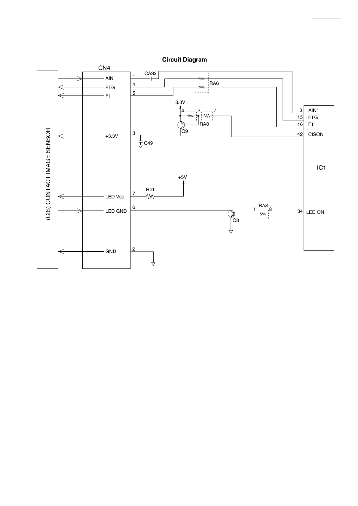
6.4.4. Scanning Block
The scanning block of this device consists of a control circuit and a contact image sensor made up of a celfoc lens array, an LED
array, and photoelectric conversion elements.
When an original document is inserted and the start button pressed, pin 34 of IC1 goes to a high level and the transistor Q8 turns
on.This applies voltage to the LED array to light it. The contact image sensor is driven by each of the FTG-F1 signals output from
IC1, and the original image illuminated by the LED array undergoes photoelectric conversion to output an analogue image signal
(AIN). The analogue image signal is input to the system ASIC on AIN1 (pin 3 of IC1) and converted into 8-bit data by the A/D converter inside IC1. Then this signal undergoes digital processing in order to obtain a high-quality image.
27
KX-FP701LA
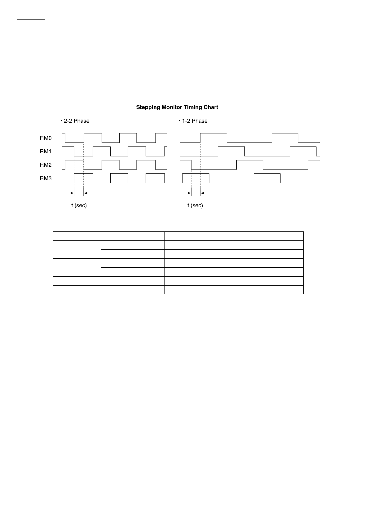
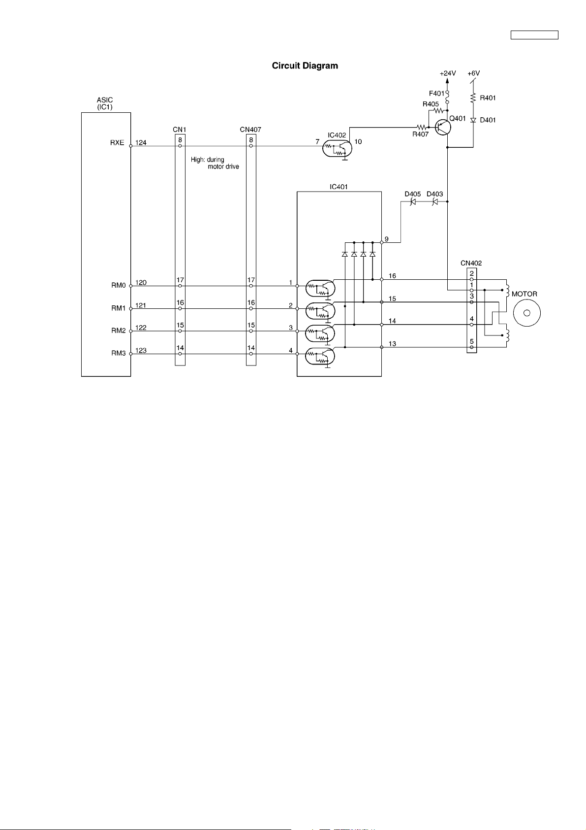
6.4.5. Stepping Motor Drive Circuit (RX)
1. Function
The stepping motor works for reception and copy.
2. Motor
During motor driving, pin 124 of ASIC IC1 becomes high level, IC401 10pin becomes low level, and Q401 turns ON. As a
result, +24V is supplied to the motor coil.
Stepping pulses are output from ASIC IC1 pins, 124, 120~123, causing driver IC401 pins, 16~13 to drive the Motor Coil. The
motor coil is energized sequentially in 2 phase increments, which causes a 1-step rotation.
The timing chart is below.
Stepping Motor Drive Mode
Function Mode Phase Pattern Speed
Copy Fine, Photo 1-2 432 pps (t=1/432)
Super Fine 1-2 216 pps (t=1/216)
FAX Receiving Standard, Fine, Photo 1-2 432 pps (t=1/432)
Super Fine 1-2 216 pps (t=1/216)
Paper Feed ——— 1-2 432 pps (t=1/432)
Stand-by ——— All phases are currently off. None
28
KX-FP701LA
When the motor suspends while it is in the receive mode (about 70~80 msec), pin 124 of ASIC IC1 becomes a low level and Q401
turns OFF, and instead of +24 V, +6 V is supplied through D401 so that the motor is held in place. When the system is in the standby mode, all of the motor drive transistors turn OFF. Consequently, the motor current stops.
29
KX-FP701LA
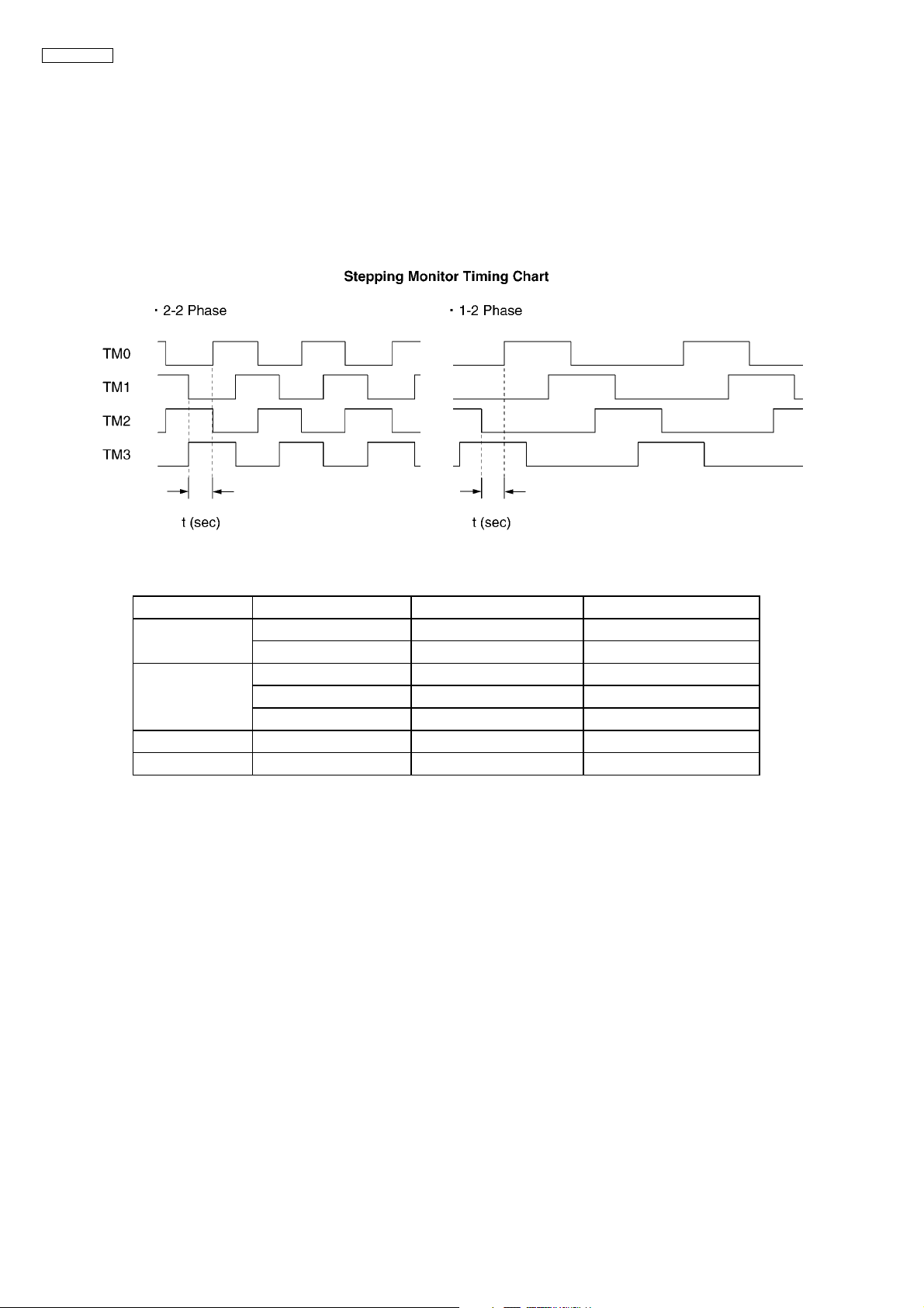
6.4.6. Stepping Motor Drive Circuit (TX)
1. Function
The stepping motor works for reception and copy.
2. Motor
During motor driving, pin 131 of ASIC IC1 becomes high level, IC401 10pin becomes low level, and Q402 turns ON. As a
result, +24V is supplied to the motor coil.
Stepping pulses are output from ASIC IC1 pins, 131, 125, 128~130, causing driver IC402 pins, 16~13 to drive the Motor Coil.
The motor coil is energized sequentially in 2 phase increments, which causes a 1-step rotation.
The timing chart is below.
Stepping Motor Drive Mode
Function Mode Phase Pattern Speed
Copy Fine, Photo 1-2 432 pps (t=1/432)
Super Fine 1-2 216 pps (t=1/216)
FAX Sending Standard 1-2 432 pps (t=1/432)
Fine, Photo 1-2 432 pps (t=1/432)
Super Fine 1-2 216 pps (t=1/216)
Document Feed ——— 1-2 432 pps (t=1/432)
Stand-by ——— All phases are currently off. None
30
 Loading...