

Panasonic EZAST-SS, EZACT, EZASTB-SSB, EZANT, EZADT User Manual
Chip RC Networks
Type:
EZACT
EZADT
EZAST/SS
EZANT
GND GND
Type:
EZASTB/SSB
Chip RC Networks
GND
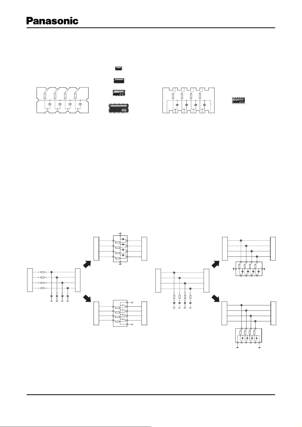
■ Features
Smallest SMD R/C networks
● 4 popular noise reduction circuits made
EZACT : 2.0 mm ҂ 1.2 mm ҂ 0.6 mm, 0.5 mm pitch (Flat terminal type)
EZADT : 3.2 mm ҂ 1.6 mm ҂ 0.65 mm, 0.635 mm pitch (Concave terminal type)
EZAST/SS : 4.0 mm ҂ 2.1 mm ҂ 0.65 mm, 0.8 mm pitch (Concave terminal type)
EZASTB/SSB : 4.0 mm ҂ 2.1 mm ҂ 0.65 mm, 0.65 mm pitch (Convex terminal type)
EZANT : 6.4 mm ҂ 3.1 mm ҂ 0.80 mm, 1.27 mm pitch (Concave terminal type)
● Takes up less space than discrete chip resistor & chip capacitor
EZACT:25 % of 0402 inches (1.0 mm ҂ 0.5 mm) chips placing area
EZADT:50 % of 0402 inches (1.0 mm ҂ 0.5 mm) chips placing area
EZAST/SS, EZASTB/SSB:70 % of 0402 inches (1.0 mm ҂ 0.5 mm) chips placing area
EZANT:55 % of 0805 inches (2.0 mm ҂ 1.2 mm) chips placing area
<Effect of high density placing, PWB space saving>
RC Low pass fi lter AC Terminator
I/O I/O
GND
I/O I/O
(EZACT, EZADT, EZAST/SS, EZANT)
I/O I/O
Discrete Chips
Chip RC Network
I/O I/O
Chip RC Network
(EZASTB/SSB)
I/O I/O
Discrete Chips
(EZACT, EZADT, EZAST/SS, EZANT)
Chip RC Network
I/O I/O
Chip RC Network
(EZASTB/SSB)
■ Recommended Applications
● Digital equipment such as PCs, printers, HDD, PCMCIA cards, PDAs, and word processors
● Communication equipment, digital cordless phones, automobile phones, GSM, PHS, DECT
● Digital audio and video equipment
● Electronic musical instruments, and other digital devices
Design and spec ifi cations are e ach subj ect to change w ithout notic e. Ask f actory for t he cur rent technical speci fi cations before purchase and/or use.
Should a sa fet y concern ar ise reg arding th is product, please be sure to c ontac t us immediately.
Feb. 2006
■ Explanation of Part Numbers
EZACT (R/C Standard Combination)
●
1
2
3
Chip RC Networks
4
5
6
7
8
9
10
11 12
E
Thick Film Noise
Suppression and
Filtering
Components
EZADT • EZAST • EZANT (R/C Standard Combination)
●
1
E
Thick Film Noise
Suppression and
Filtering
Components
Z
Common Code
CT
2
Z
Common Code
3.2 mm
DT
҂1.6 mm
4.0 mm
ST
҂2.1 mm
6.4 mm
NT
҂3.1 mm
A
2.0 mm
҂1.2 mm
3
A
C
Dimension and
Circuit Configuration
Chip RC
Networks
4
S
Dimension and
Circuit Configuration
Chip RC
Networks
T
0
1
2
3
4
5
6
5
T
Resistance Value
Configuration
1
2
3
4
5
6
Resistance Value
Configuration
✽ 220 pF to 1000 pF available for EZANT, 22 pF to 100 pF available for EZAST, EZADT
•
EZACT
●
EZADT • EZASS • EZANT (R/C Except the standard Combination)
1
2
3
4
5
3
R/C Standard Combination
10 액
22 액
47 액
100 액
220 액
470 액
1k액
6
3
R/C Standard Combination
22 액
47 액
100 액
220 액
470 액
1k액
6
0
Capacitance Value
Configuration
0
1
7
3
Capacitance Value
Configuration
1
2
3
4
5
6
7
A
10 pF
22 pF
8
A
22 pF
47 pF
100 pF
220 pF
470 pF
1000 pF
8
A
Design
Configuration
9
A
Design
Configuration
✽
AAA
9
AAA
A
10
A
Standard
10
Resistance
Tolerance
Standard
11 12
J
Resistance
Tolerance
J
Suffix for Special
Requirement
J ±5%
Suffix for Special
Requirement
J ±5%
11 12
E
Thick Film Noise
Suppression and
Filtering
Components
EZASTB (R/C Standard Combination)
●
1
E
Thick Film Noise
Suppression and
Filtering
Components
Z
Common Code
2
Z
Common Code
4.0 mm
STB
҂2.1 mm
CT
DT
SS
NT
A
2.0mm
҂1.2 mm
3.2 mm
҂1.6 mm
4.0 mm
҂2.1 mm
6.4 mm
҂3.1 mm
3
A
Convex
terminal type
Chip RC
Networks
S
Dimension and
Circuit Configuration
4
S
Circuit Configuration
S
Chip RC
Networks
5
T
Dimension and
Resistance Value
Configuration
1
2
3
4
5
6
7
CT
DT
SS
NT
6
B
22 액
47 액
100 액
220 액
470 액
1k액
0
Resistance Value : 10 액 to 100 k액
Capacitance Value : 10 pF to 33 pF
In above-mentioned range, it is possible to
choose optional R/C.
Resistance Value : 10 액 to 100 k액
Capacitance Value : 10 pF to 100 pF
In above-mentioned range, it is possible to
choose optional R/C.
Resistance Value : 10 액 to 100 k액
Capacitance Value : 10 pF to 180 pF
In above-mentioned range, it is possible to
choose optional R/C.
Resistance Value : 10 액 to 100 k액
Capacitance Value : 220 pF to 1000 pF
In above-mentioned range, it is possible to
choose optional R/C.
7
3
R/C Standard Combination
Capacitance Value
Configuration
1
2
3
1
Design Number
8
3
22 pF
47 pF
100 pF
Y
9
A
Design
Configuration
AA
A
10
A
Standard
J
Resistance
Tolerance
J
11 12
J
Resistance
Tolerance
Suffix for Special
Requirement
±5%
Suffix for Special
Requirement
J ±5%
Design and spec ifi cations are e ach subj ect to change w ithout notic e. Ask f actory for t he cur rent technical speci fi cations before purchase and/or use.
Should a sa fet y concern ar ise reg arding th is product, please be sure to c ontac t us immediately.
Feb. 2006
■ Explanation of Part Numbers
● EZASSB (R/C Except the standard Com bi na tion)
1
2
3
4
5
Chip RC Networks
6
7
8
9
10
11 12
E
Thick Film Noise
Suppression and
Filtering
Components
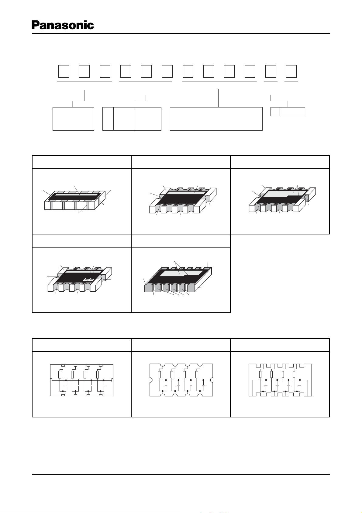
■ Construction
Protective coating
Marking
Z
Common Code
A
SSB
S
Dimension and
Circuit Configuration
Convex
4.0 mm
҂2.1 mm
terminal type
Chip RC
Networks
S
B
7
Resistance Value : 10 액 to 100 k액
Capacitance Value : 10 pF to 180 pF
In above-mentioned range, it is possible to
choose optional R/C.
0
Design Number
1
A
J
Resistance
Tolerance
J ±5%
EZACT EZADT EZAST/SS
Marking
Electrode
(Outer)
GND
Electrode
(Outer)
Alumina substrate
GND
Electrode
(Outer)
Protective coating
Electrode
(Outer)
Electrode
(Outer)
Alumina substrate
GND
Electrode
(Outer)
Alumina substrate
GND
Electrode
(Outer)
Protective coating
EZANT EZASTB/SSB
Suffix for Special
Requirement
Marking
33
GND
Electrode
(Outer)
Alumina substrate
GND
Electrode
(Outer)
Protective coating
Marking
Electrode
(Outer)
GND
Electrode
(Outer)
■ Circuit Confi guration
EZACT EZADT
10 9 8 7
GND GND
R1 R2 R3 R4
C1 C2 C3 C4
2345
R1=R2=R3=R4
C1=C2=C3=C4
61
Marking
GND
Electrode
(Outer)
Protective coating
•
EZAST/SS
10 9 8 7
GND GND
R1C1R2C2R3 R4
2345
R1=R2=R3=R4
C1=C2=C3=C4
33
Electrode
(Outer)
Alumina substrate
GND
Electrode
(Outer)
•
EZANT EZASTB/SSB
C3 C4
61
10 9 8 7
1112
R1C1R2C2R3 R4
C3
234 5 61
C1=C2=C3=C4
C4
GNDGND R1=R2=R3=R4
Design and spec ifi cations are e ach subj ect to change w ithout notic e. Ask f actory for t he cur rent technical speci fi cations before purchase and/or use.
Should a sa fet y concern ar ise reg arding th is product, please be sure to c ontac t us immediately.
Feb. 2006
 Loading...