

Page 1
ORDER NO.DSD1003007CE
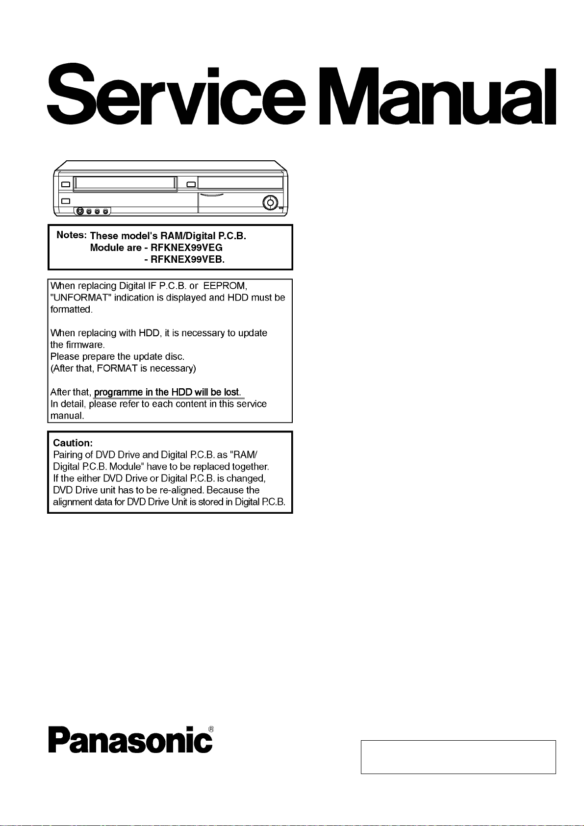
DVD Recorder
Model No. DMR-EX99VEB
DMR-EX99VEG
Vol. 1
Colours
(K).......................Black Type
(S).......................Silver Type (Only EX99VEG)
© Panasonic Corporation 2010.
Unauthorized copying and distribution is a violation
of law.
Page 2
TABLE OF CONTENTS
1 Safety Precaution-------------------------------------------------3
1.1. General guidelines-----------------------------------------3
2Warning--------------------------------------------------------------4
2.1. Prevention of Electrostatic Discharge (ESD)
to Electrostatic Sensitive (ES) Devices---------------4
2.2. Precaution of Laser Diode -------------------------------5
2.3. Service caution based on legal restrictions----------6
3 Service Navigation------------------------------------------------7
3.1. Service Information----------------------------------------7
3.2. Caution for DivX--------------------------------------------7
3.3. Micro Fuse conducting check---------------------------8
3.4. Operation check when a USB device is
connected----------------------------------------------------9
4 Specifications----------------------------------------------------10
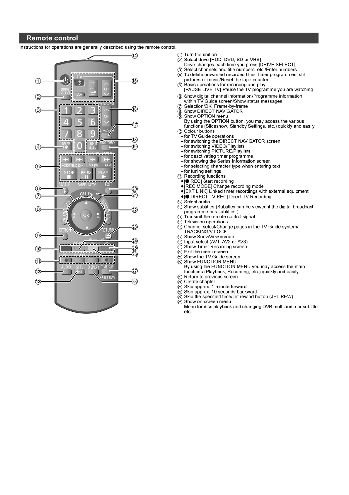
5 Location of Controls and Components------------------13
5.1. Each Buttons----------------------------------------------13
6 Operation Instructions----------------------------------------15
6.1. (DVD) Taking out the Disc from DVD-Drive
Unit when the Disc cannot be ejected by
OPEN/CLOSE button -----------------------------------15
6.2. (VHS) Removing Cassette T a pe manually --------17
7 Service Mode-----------------------------------------------------19
7.1. (DVD) Self-Diagnosis and Special Mode
Setting-------------------------------------------------------19
PAGE PAGE
7.2. (VHS) Self-Diagnosis and Special Mode
Setting------------------------------------------------------ 35
8 Service Fixture & Tools--------------------------------------- 39
9 Assembling and Disassembling Instructions--------- 40
9.1. Disassembly Flow Chart------------------------------- 40
9.2. P.C.B. Positions------------------------------------------ 41
9.3. Caution with inserting cassette tape when
disassembling the unit---------------------------------- 42
9.4. Top Case--------------------------------------------------- 43
9.5. Front Panel------------------------------------------------ 43
9.6. Front Jack P.C.B., FL Drive P.C.B. ------------------ 44
9.7. VHS Mechanism Unit----------------------------------- 46
9.8. RAM/Digital P.C.B. Module---------------------------- 47
9.9. SD/ USB P.C.B. ------------------------------------ ------ 48
9.10. Rear Panel, Fan Motor--------------------------------- 49
9.1 1 . HDMI P.C.B.----------------------------------------------- 49
9.12. Digital IF P.C.B. ------------------------------------------ 49
9.13. HDD--------------------------------------------------------- 50
9.14. Backend P.C.B.------------------------------------------- 51
9.15. Main P.C.B.------------------------------------------------ 51
10 Measurements and Adjustments-------------------------- 52
10.1. Service Positions ---------------------------------------- 52
10.2. Caution for Replacing Parts--------------------------- 56
10.3. (DVD) Standard Inspection Specifications
after Making Repairs------------------------------------ 60
2
Page 3
1 Safety Precautions
1.1. General guidelines
1. When servicing, observe the original lead dress. If a short circuit is found, re place all parts which have been overheated or
damaged by the short circuit.
2. After servicing, see to it that all the protective devices such as insulation barriers, insulation papers shields are properly
installed.
3. After servicing, make the following leakage current checks to prevent the customer from being exposed to shock hazards.
1.1.1. Leakage current cold check
1. Unplug the AC cord and connect a jumper between the
two prongs on the plug.
2. Measure the resistance value, with an ohmmeter,
between the jumpered AC plug and each exposed metallic cabinet part on the equipment such as screwheads,
connectors, control shafts, etc. When the exposed metallic part has a return path to the chassis, the reading
should be between 1MΩ and 5.2MΩ.
When the exposed metal does not have a return path to
the chassis, the reading must be .
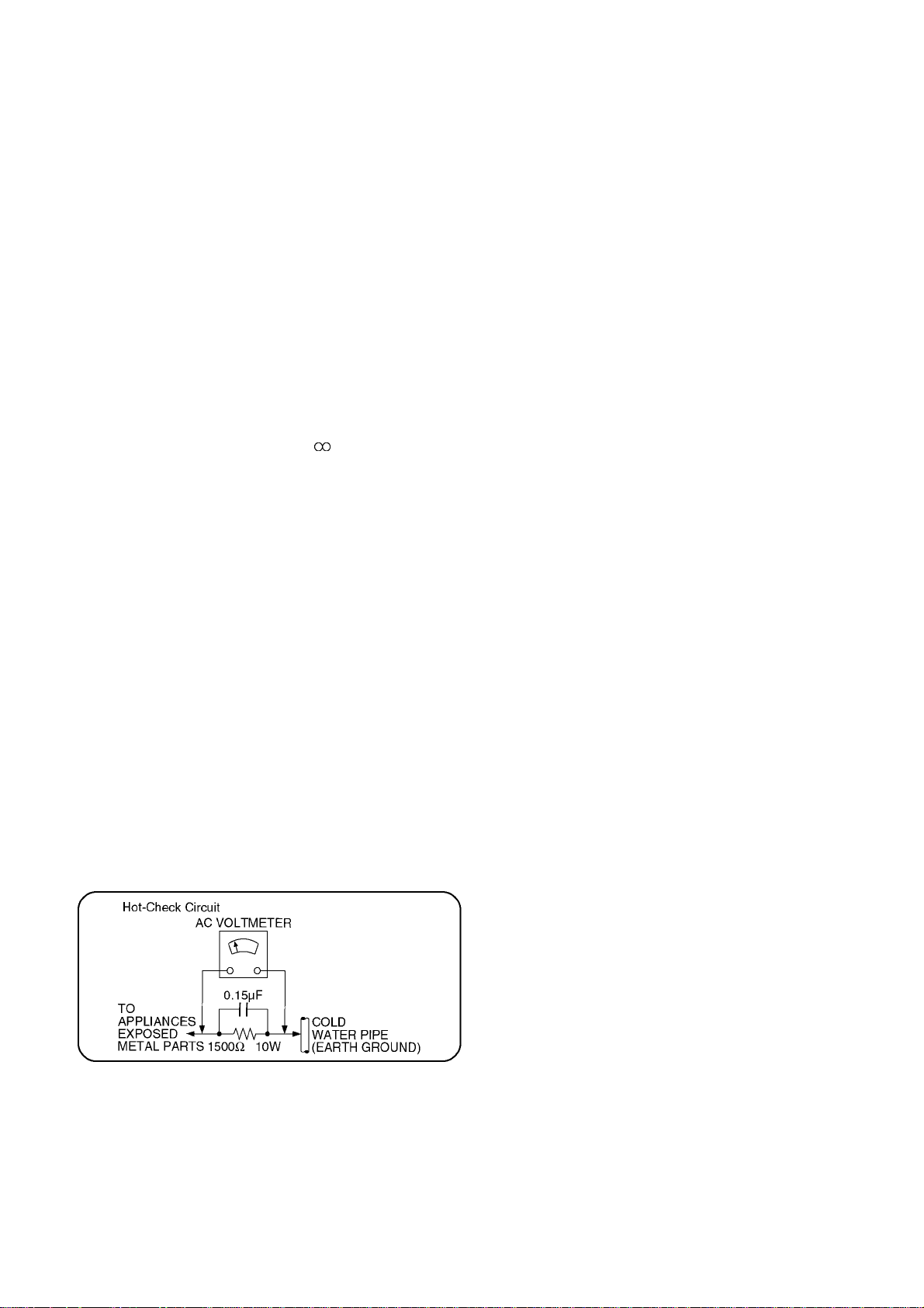
1.1.2. Leakage current hot check
(See Figure 1.)
1. Plug the AC cord directly into the AC outlet. Do not use
an isolation transformer for this check.
2. Connect a 1.5kΩ, 10 watts resistor, in parallel with a
0.15μF capacitors, between each exposed metallic part
on the set and a good earth ground such as a water pipe,
as shown in Figure 1.
3. Use an AC voltmeter, with 1000 ohms/volt or more sensitivity , to measure the potential across the resistor.
4. Check each exposed metallic part, and measure the voltage at each point.
5. Reverse the AC plug in the AC outlet and repeat each of
the above measurements.
6. The potential at any point should not exceed 0.75 volts
RMS. A leakage current tester (Simpson Model 229 or
equivalent) may be used to make the hot checks, leakage
current must not exceed 1/2 milliampere. In case a measurement is outside of the limits specified, there is a possibility of a shock hazard, and the equipment should be
repaired and rechecked before it is returned to the customer.
Figure 1
3
Page 4

2Warning
2.1. Prevention of Electrostatic Discharge (ESD) to Electrostatic Sensitive
(ES) Devices
Some semiconductor (solid state) devices can be damaged easily by static electricity. Such components commonly are called Electrostatic Sensitive (ES) Devices. Examples of typical ES devices are integrated circuits and some field-effect transistor-sand semiconductor "chip" components. The following techniques should be used to help reduce the incidence of component damage
caused by electrostatic discharge (ESD).
1. Immediately before handling any semiconductor component or semiconductor-equipped assembly, drain off any ESD on your
body by touching a known earth ground. Alternatively, obtain and wear a commercially available discharging ESD wrist strap,
which should be removed for potential shock reasons prior to applying power to the unit under test.
2. After removing an electrical assembly equipped with ES devices, place the assembly on a conductive surface su ch as a luminum foil, to prevent electrostatic charge buildup or exposure of the assembly.
3. Use only a grounded-tip soldering iron to solder or unsolder ES devices.
4. Use only an anti-static solder removal device. Some solder removal devices not classified as "anti-static (ESD protected)" can
generate electrical charge sufficient to damage ES devices.
5. Do not use freon-propelled chemicals. These can generate electrical charges sufficient to damage ES devices.
6. Do not remove a replacement ES device from its protective package until immediately before you are ready to install it. (Most
replacement ES devices are packaged with leads electrically shorted together by conductive foam, aluminum foil or comparable conductive material).
7. Immediately before removing the protective material from the leads of a replacement ES device, touch the protective material
to the chassis or circuit assembly into which the device will be installed.
Caution
Be sure no power is applied to the chassis or circuit, and observe all other safety precautions.
8. Minimize bodily motions when handling unpackaged replacement ES devices. (Otherwise harmless motion such as the
brushing together of your clothes fabric or the lifting of your foot from a carpet ed floor can generate static electricity sufficient
to damage an ES device).
4
Page 5
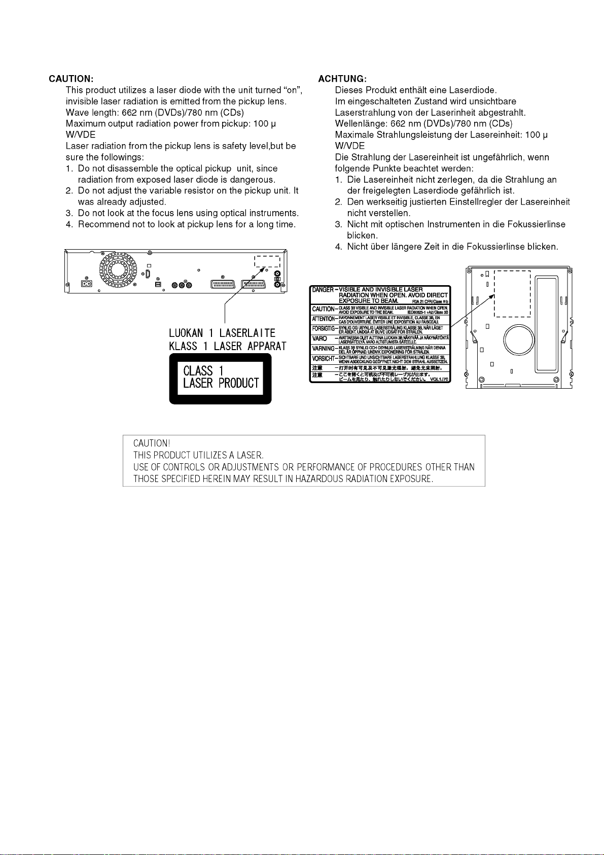
2.2. Precaution of Laser Diode
5
Page 6

2.3. Service caution based on legal restrictions
2.3.1. General description about Lead Free Solder (PbF)
The lead free solder has been used in the mounting process of all electrical comp onents on the printed circuit boards us ed for this
equipment in considering the globally environmental conservation.
The normal solder is the alloy of tin (Sn) and lead (Pb). On the other hand, the lead free solder is the alloy mainly consists of tin
(Sn), silver (Ag) and Copper (Cu), and the melting point of the lead free solder is higher approx.30 degrees C (86°F) more than that
of the normal solder.
Definition of PCB Lead Free Solder being used
The letter of “PbF” is printed either foil side or components side on the PCB using the lead free solder.
(See right figure)
Service caution for repair work using Lead Free Solder (PbF)
• The lead free solder has to be used when repairing the equipment for which the lead free solder is used.
(Definition: The letter of “PbF” is printed on the PCB using the lead free solder.)
• To put lead free solder, it should be well molten and mixed with the original lead free solder.
• Remove the remaining lead free solder on the PCB cleanly for soldering of the new IC.
• Since the melting point of the lead free solder i s higher than that of the normal lead solder, it takes the longer time to melt the
lead free solder.
• Use the soldering iron (more than 70W) e quipped with the tempe rature control after setting the te mperature at 350±30 degrees
C (662±86°F).
Recommended Lead Free Solder (Service Parts Route.)
• The following 3 types of lead free solder are available through the service parts route.
RFKZ03D01KS-----------(0.3mm 100g Reel)
RFKZ06D01KS-----------(0.6mm 100g Reel)
RFKZ10D01KS-----------(1.0mm 100g Reel)
Note
* Ingredient: tin (Sn), 96.5%, silver (Ag) 3.0%, Copper (Cu) 0.5%, Cobalt (Co) / Germanium (Ge) 0.1 to 0.3%
6
Page 7
3 Service Navigation
3.1. Service Information
3.2. Caution for DivX
7
Page 8
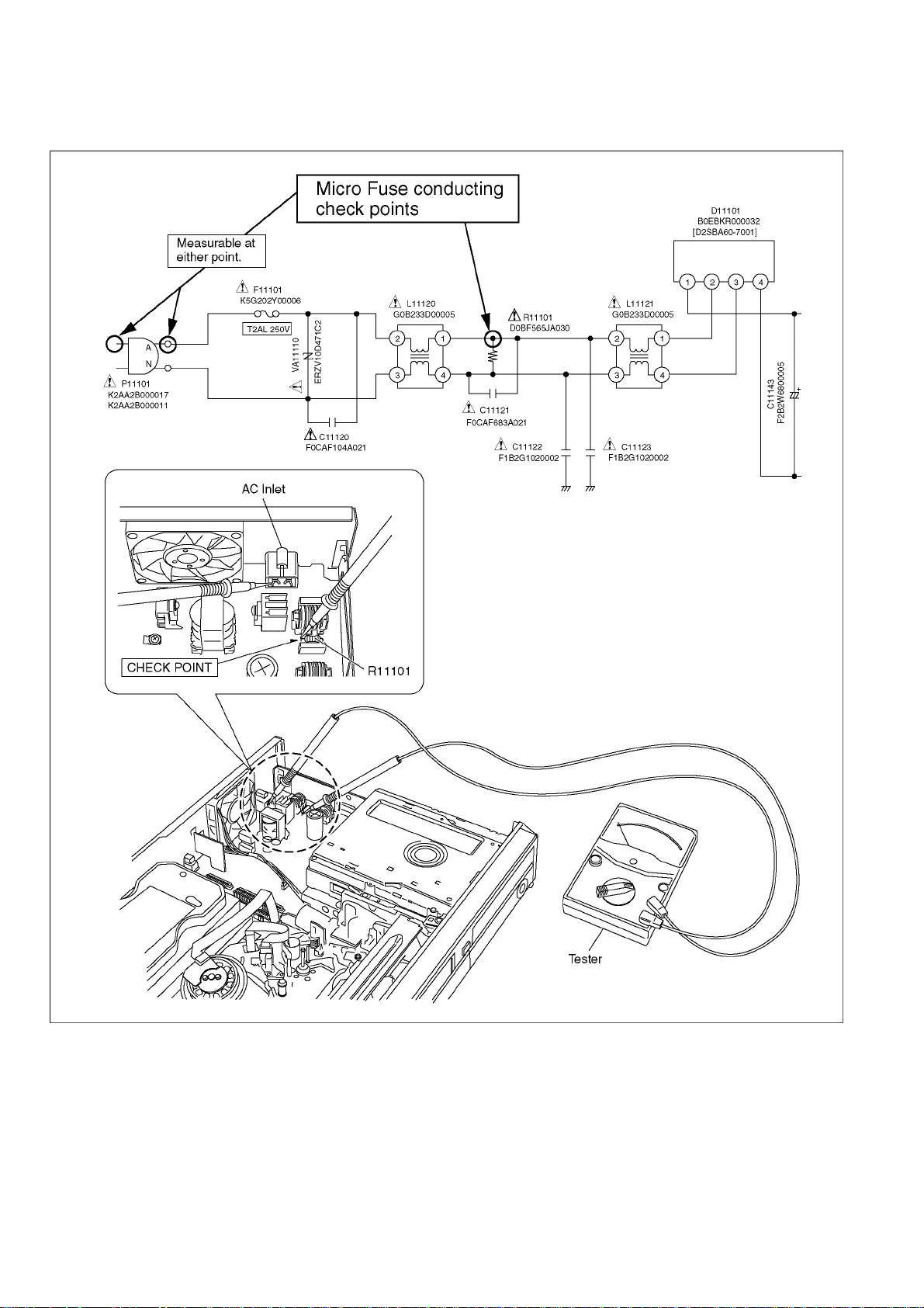
3.3. Micro Fuse conducting check
This unit uses the Micro Fuse.
Check the Micro Fuse conducting using the Tester at the check points below.
8
Page 9
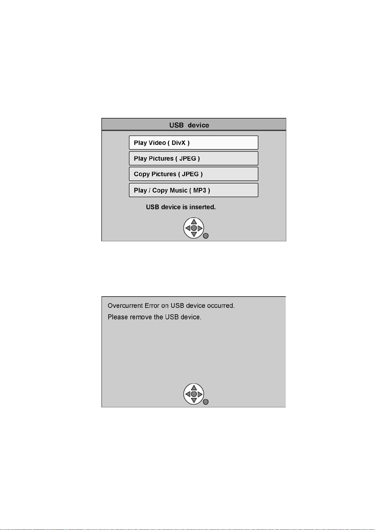
3.4. Operation check when a USB device is connected
You can check the operation status (normal or abnormal) of the USB connection part of this unit easily as shown below.
Connect each device to the USB terminal on the front panel and check the operation status on the TV monitor.
Normal operation:
Automatically displayed when the USB connection is made to a digital camera, etc.
(Example below: When JPEG materials have been recorded)
(*Displayed items differ depending on the recorded contents.)
Abnormal operation (Example 1):
Warning is displayed automatically if overcurrent is detected when a USB device is connected.
(*When a USB device or this unit’s USB terminal shorts out or the power supp ly type of USB device is connecte d)
Abnormal operation (Example 2):
When the terminal of USB device is damaged or open, there is no display on the TV monitor.
9
Page 10
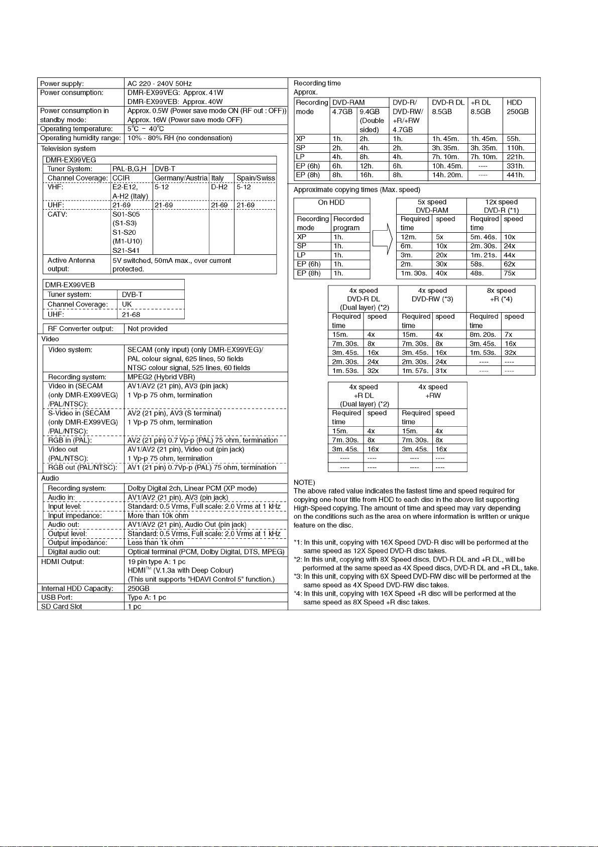
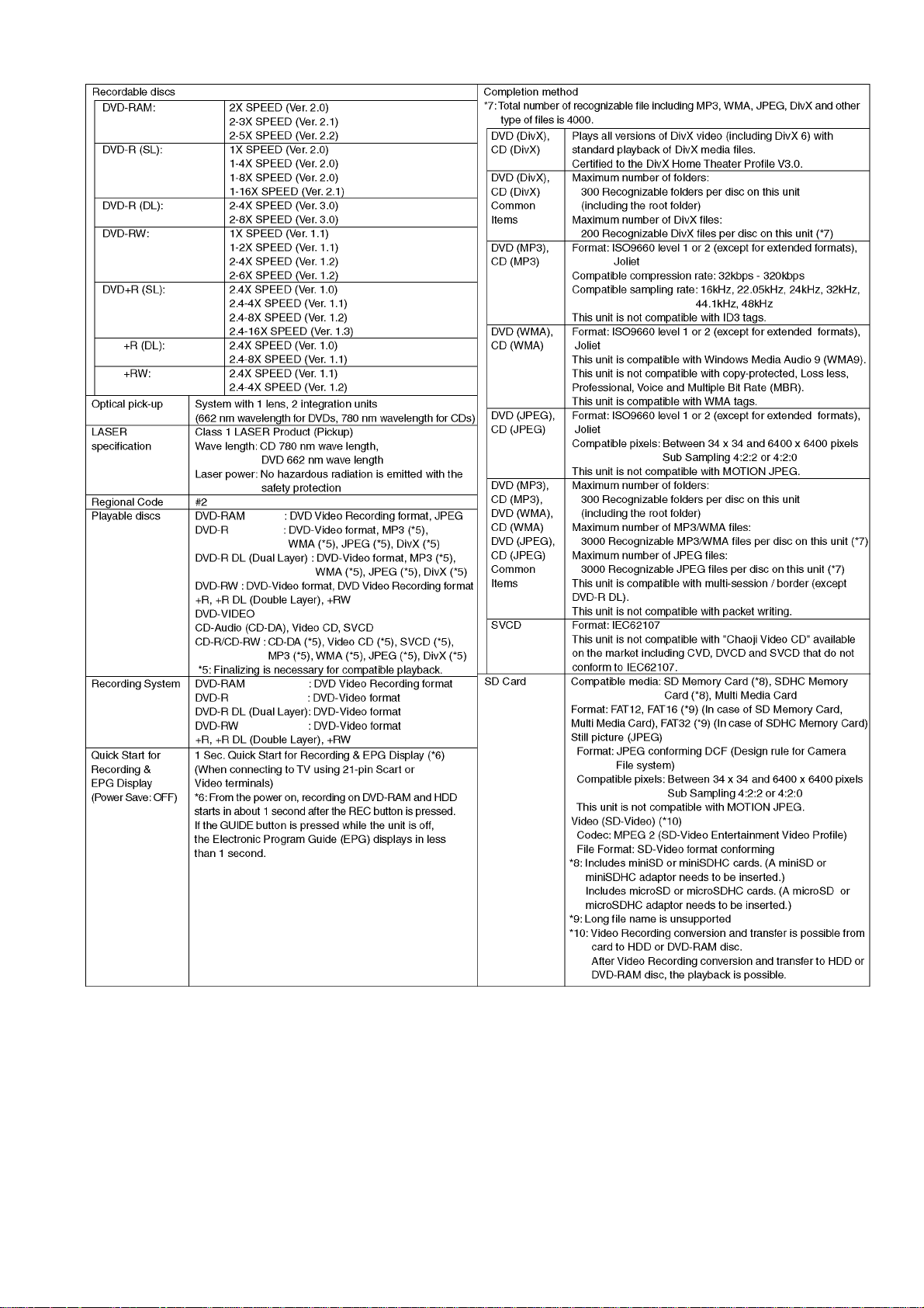
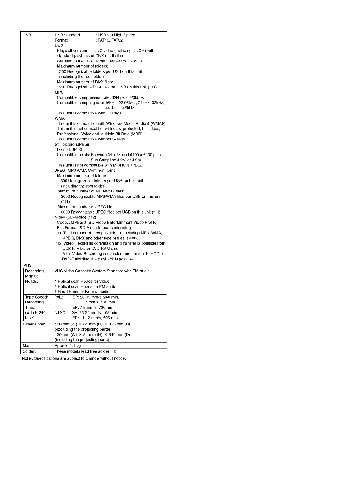
4 Specifications
10
Page 11
111213
Page 12
Page 13

5 Location of Controls and Components
5.1. Each Buttons
Followings are the Location of Controls and Components for DMR-EX99VEG as a sample.
For other model, refer to each Operation Instructions.
Page 14
14
Page 15
6 Operating Instructions
6.1. (DVD) Taking out the Disc from DVD-Drive Unit when the Disc cannot be
ejected by OPEN/CLOSE button
6.1.1. (DVD) Forcible Disc Eject
6.1.1.1. (DVD) When the power can be turned off.
1. Turn off the power and press [STOP], [CH UP] keys on the front panel simultaneously for 5 seconds.
6.1.1.2. (DVD) When the power can not be turned off.
1. Press [POWER] key on the front panel for over 4 seconds to turn off the power forcibly, and press [STOP] [CH UP] keys on
the front panel simultaneously for 5 seconds.
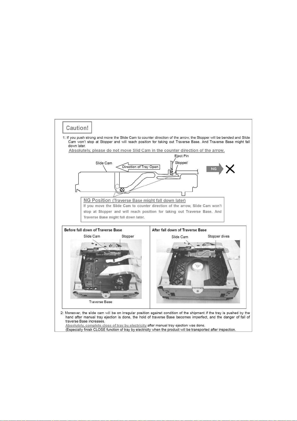
6.1.2. (DVD) When the Forcible Disc Eject can not be done.
15
Page 16
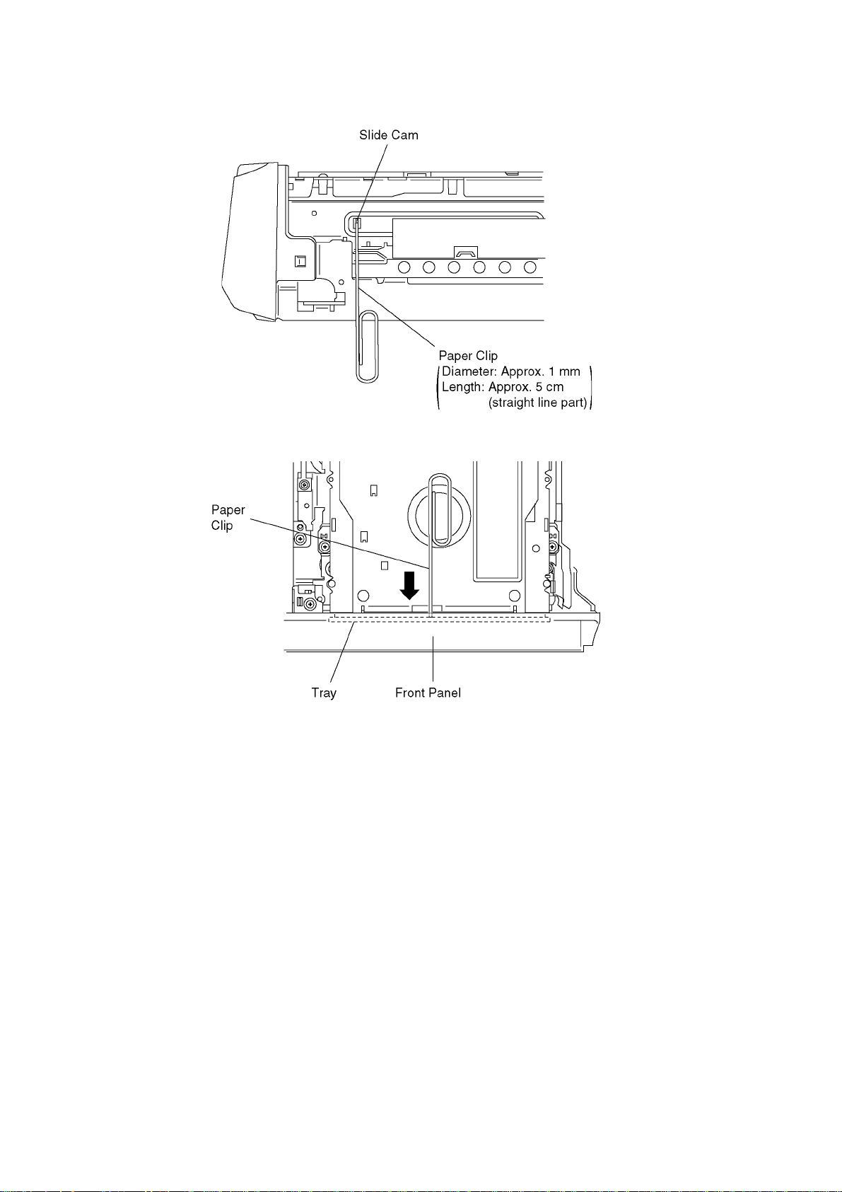
1. Turn off the power and pull out AC cord.
2. Remove the Top Case.
3. Push in SLIDE CAM by Paper Clip or minus screw driver (small) to eject tray slightly.
4. Push out Tray by Paper Clip or minus screw driver (small).
16
Page 17
6.2. (VHS) Removing Cassette Tape
manually
When the cassette tape could not be uninstalled from an electrical malfunction, there are 2 ways to remove a cassette tape.
6.2.1. (VHS) Removal by compulsory
unloading.
If Service Mode can be activated when the power can not be
turned on, this operation is able.
1. Press [STOP] and [EJECT] button simultaneously for
more than 3 seconds to turn the unit in VHS service
mode.
2. Press [STOP] and [EJECT] button simultaneously 7 times
to turn the unit in VHS Service Mode “7”.
3. Press [STOP] button in order to unload the mechanism.
(Pay attention to tape slack)
Service Mode Display:
7 ** ** (STOP) → 7 0L ** (EJECT)
6.2.2. (VHS) Removal by manual operation by rotating the Loading Motor
with the batteries.
1. Disconnect the AC plug, and remove the Top Panel and
the Front Panel by referring to the Disassembly Procedures.
2. Connect three batteries (1.5V spec.) to the Loading Motor
in series for supplying 4.5V to rotate the Loading Motor as
shown below.
3. Stop unloading just before unloading will be completed as
shown below, and then the tape becomes slack as shown
below.
4. Rotate the S-Reel by a small minus screwdriver to
remove the slack tape as shown below.
5. Then unload again to remove the cassette tape as shown
below.
17
Page 18
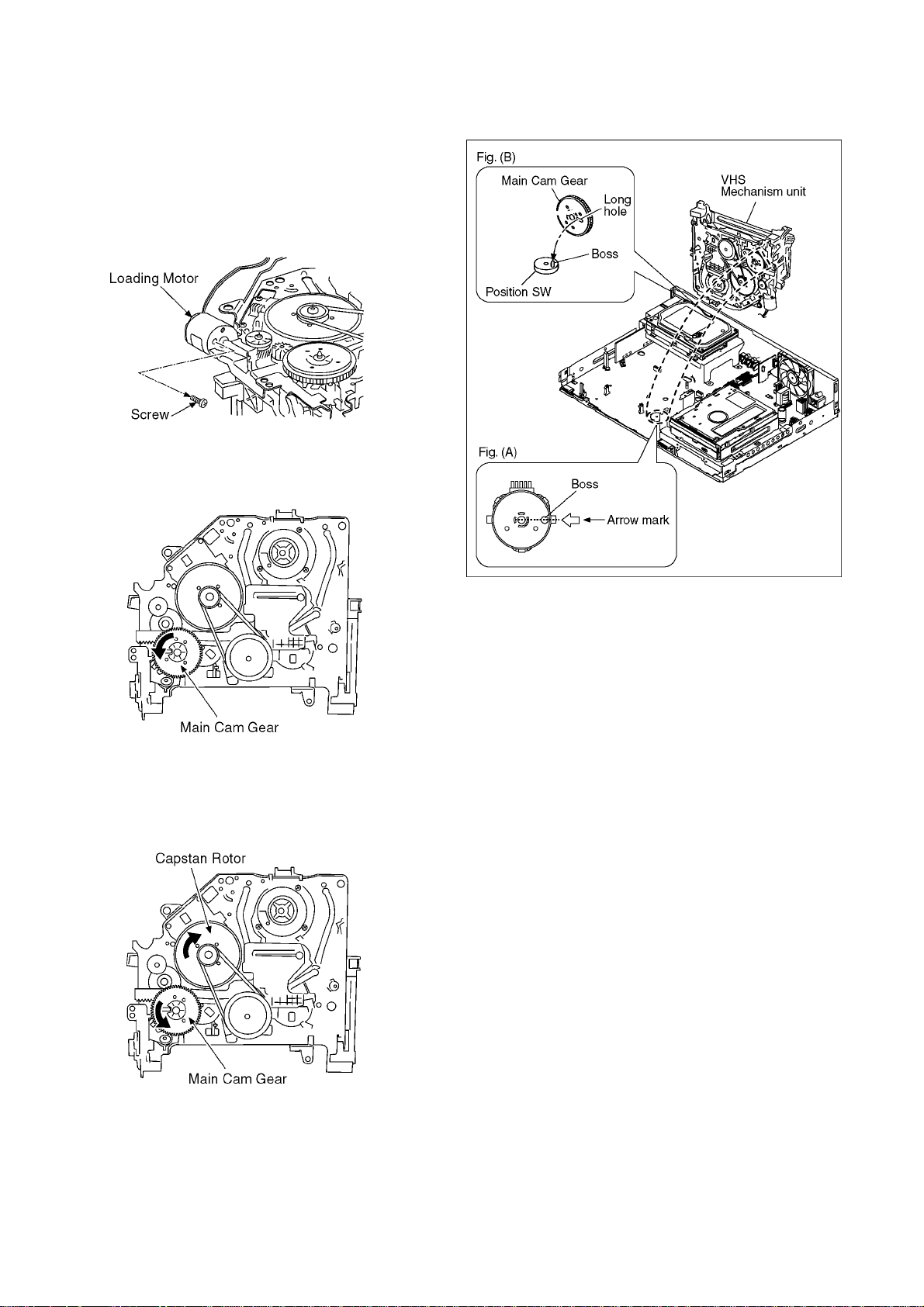
6.2.3. (VHS) Take out Cassette Tape manually after removing the mechanism
1. Disconnect the AC plug, and remove the Top Panel, Front
Panel and the Mechanism by referring to "9 Assembling
and Disassembling"
2. Remove the Screw and remove the Loading Motor as
shown below.
3. Rotate the Main Cam Gear counter-clockwise until just
before the unloading will be completed as shown below.
6. Attach Loading Motor and tighten the screw.
7. Set the Position Switch to EJECT POSITION certainly
and attach the mechanism to chassis as shown below.
4. Rotate the Capstan Motor clockwise to remove the slack
tape as shown below.
5. Rotate the Main Cam Gear counter-clockwise again to
remove the cassette-tape as shown below.
18
Page 19
7 Service Mode
7.1. (DVD) Self-Diagnosis and Special Mode Setting
7.1.1. (DVD) Self-Diagnosis Functions
Self-Diagnosis Function provides information for errors to service personnel by “Self-Diagnosis Display” when any error has
occurred.
U**, H** and F** are stored in memory and held.
You can check latest error code by transmitting [0] [1] of Remote Controller in Service Mode.
Automatic Display on FL will be cancelled when the power is turned off or AC input is turned off during self-diagnosis display is ON.
Error Code Diagnosis contents Description Monitor Display Automatic FL display
U30 Remote control code error Display appears when main unit and
remote controller codes are not matched.
U50
(For EG
only)
U59 Abnormal inner temperature
U61 The unit is carrying out its
Antenna Short U50 is displayed when a short circuit was
detected at Antenna Input while “Active
Antenna” of “Connection” of “FUNCTION
MENU” is ON,
And then “Active Antenna” is
compulsorily switched to “Off”.
Display appears when internal temperature
detected
recovery process.
of deck reaches limit temperature.
The power is turned off forcibly.
For 30 minutes after this, all key entries are
disabled. (Fan motor operates at the highest speed for the first 5 minutes. For the
remaining 25 minutes, fan motor is also
stopped.) The event is saved in memory as
well.
No display
“*” is remote controller code of the
main unit.
Display for 5 seconds.
“A short circuit was
detected at the
antenna input.
Please check your
antenna.”
No display
U59 is displayed for 30 minutes.
No display
U71 HDMI incompatible error
(HDCP incompatible)
U72 HDMI connection error
(communication error)
U73 HDMI connection error
(authentication error)
U76 HDMI connection error HDMI cannot be output because you are
Display this error when the equipment
(compatible with DVI such as TV, amplifier
etc.) connected to the unit by HDMI is
incompatible with HDCP.
*HDCP=High-bandwidth Digital Content
Protection
This error is displayed when there are any
communication problems with the unit and
the equipments (TV, amplifier etc.) connected to the unit by HDMI. (or when there
is a problem with the HDMI cable)
When authentication error occurs while the
equipments (TV, amplifier etc.) are connected by HDMI. (or when there is a problem with the HDMI cable)
connected to a model that does not support
copyright protection.
No display
No display
U72 display disappears when error
has been solved by Power OFF/ON
of connecting equipment or by
inserting/removing of HDMI cable.
No display
U73 display disappears when error
has been solved by Power OFF/ON
of connecting equipment or by
inserting/removing of HDMI cable.
No display
19
Page 20
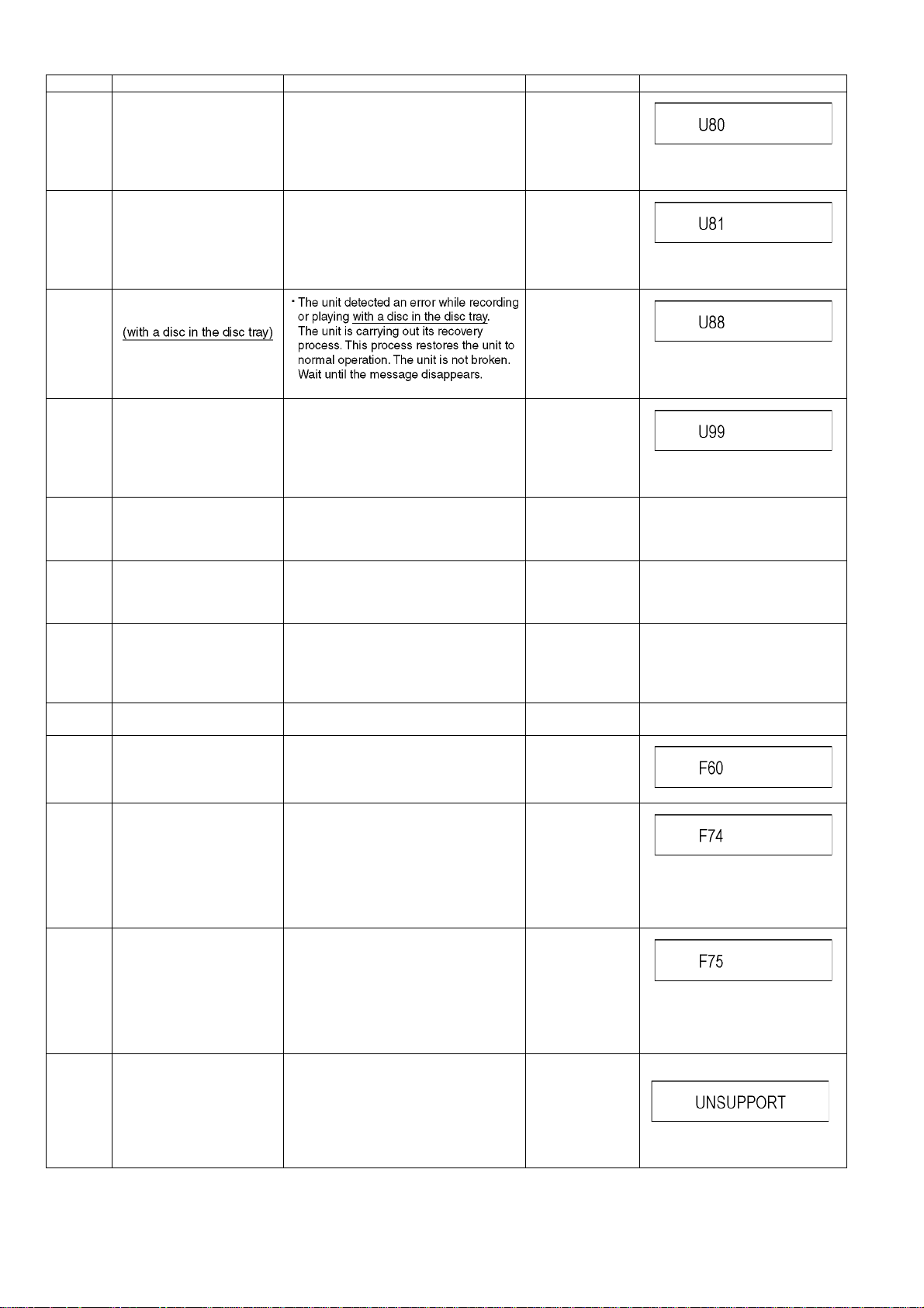
Error Code Diagnosis contents Description Monitor Display Automatic FL display
U80 ST Microprocessor
Communication Error on
Tim er Bus
U81 ST Microprocessor
Communication Error on
UART
U88 The unit is carrying out its
recovery process.
Display appears when ST Microprocessor
Communication Error on Timer Bus occurs.
Display appears when ST Microprocessor
Communication Error on DART occurs.
No display
U80 is displayed till [POWER] key is
pressed.
No display
U81 is displayed till [POWER] key is
pressed.
No display
U99 Hang-up Displayed when communication error has
H19 02 Inoperative fan motor When inoperative fan motor is detected
F00 No error information Initial setting for error code in memory
F34 Initialization error when main
microprocessor is started up
for program recording
F58 Drive hardware error When drive unit error is detected, the event
F60 DVD module has not been
F74 HDMI Device Key Communi-
F75 HDMI Device Key Information
UNSUPPORT
started.
cation error
error
Unsupported disc error *An unsupported format disc was played,
occurred between Main microprocessor
and Timer microprocessor.
after powered on, the power is turned off
automatically.
The event is saved in memory.
(Error code Initialization is possible with
error code initialization and main unit initialization.)
When initialization error is detected after
starting up main microprocessor for program recording, the power is turned off
automatically.
The event is saved in memory.
is saved in memory.
Defect of Digital P.C.B., defect of regulator
circuit for Digital P.C.B. and so on.
Mode: No change
HDMI connection could not be authenticated due to a transfer malfunction.
Factor of HDMI Device key-road failure
• When HDMI LSI is damaged.
• When the bus line of I2C doesn't operate normally.
• When device key information recorded
is damaged.
HDMI connection could not be authenticated due to an internal data malfunction.
Factor of HDMI Device key-road failure
• When HDMI LSI is damaged.
• When the bus line of I2C doesn't operate normally.
• When device key information recorded
is damaged.
although the drive starts normally.
*The data format is not supported, although
the media type is supported.
*Exceptionally in case of the disc is dirty.
No display
Displayed is left until the [POWER]
key is pressed.
No display No display
No display No display
No display No display
No display No display
No display
No display
No display
“This disc is
incompatible.”
Display for 5 seconds.
The character indication flows sideways.
20
Page 21
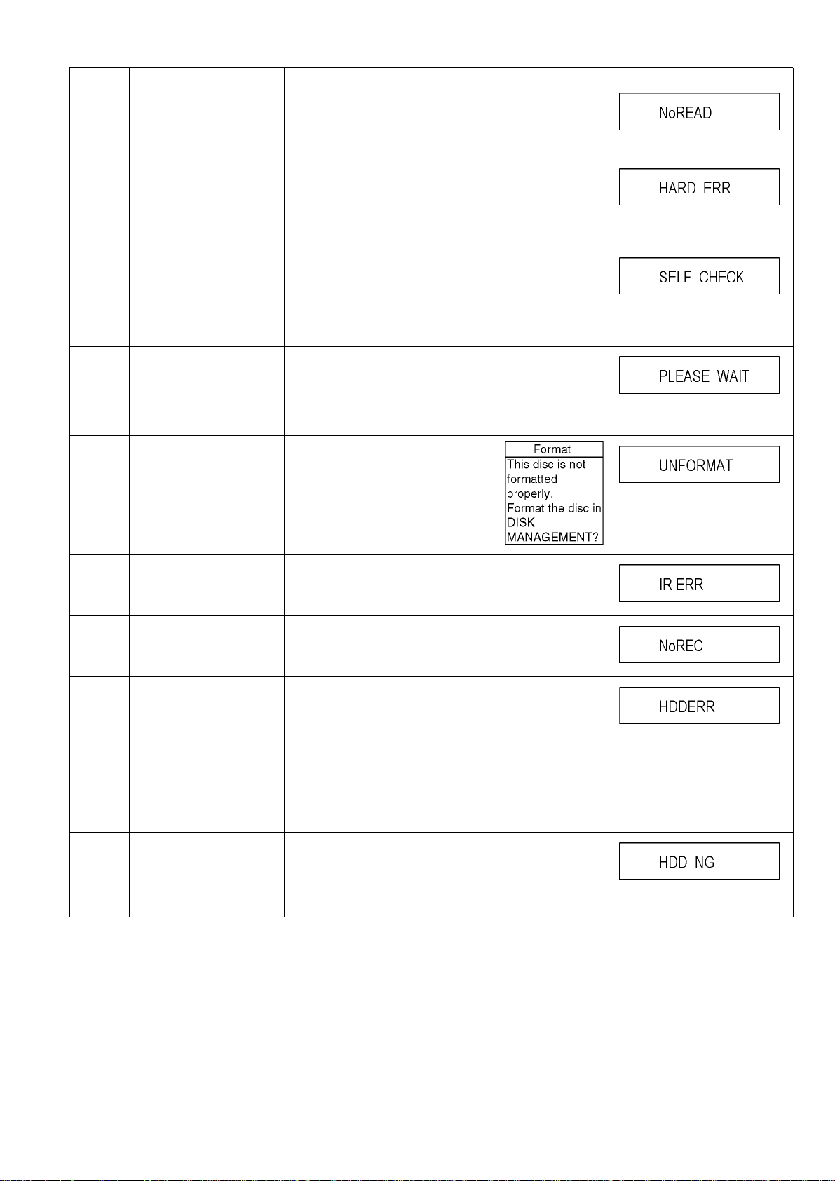
Error Code Diagnosis contents Description Monitor Display Automatic FL display
NO READ Disc read error *A disc is flawed or dirty.
*A poor quality failed to start.
*The track information could not be read.
“Cannot read.
Please check the
disc.”
HARD
ERR
SELF
CHECK
PLEASE
WAIT
UNFORMAT
Drive error The drive detected a hard error. “DVD drive error.” Display for 5 seconds.
The character indication flows sideways.
Restoration operation Since the power cord fell out during a
power failure or operation, it is under restoration operation.
*It will OK, if a display disappears automatically. If a display does not disappear, there
is the possibility that defective Digital P.C.B.
/ DVD drive.
Unit is in termination process Unit is in termination process now.
“BYE” is displayed and power will be turned
off.
In case “Quick Start” of setup menu is ON,
it is displayed in restoration operation for
AC off.
Unformatted disc error You have inserted an unformatted DVD-
RAM or DVD-RW that is unformatted or
recorded on other equipment.
No display
The character indication flows sideways.
No display
The character indication flows sideways.
The character indication flows sideways.
IR ERR IR communication error [IR ERR] is displayed when communication
No REC Recording is impossible [No REC] is displayed when recording is
HDD
ERROR
HDD NG Power on Stand-by setting
[HDD ERR] is displayed when
start up of HDD was failed.
(Except error of setting of
Power on Stand-by)
error
between Timer microprocessor and IR
microprocessor fails.
impossible due to the defect, dirt or wound
of media.
a) When normal start up was failed.
b) When start up at HDD boot was failed.
c) When start up from state of P-OFF was
failed.
d) When start up from state of HDD SLEEP
was failed.
[HDD ERR] is displayed when above each
start up of HDD was failed.
*In case b), tray opens automatically and
[HDDERR] is displayed until version up
disc is inserted.
[HDD NG] is displayed when power on
Stand-by setting of HDD is NG or when
HDD which power on Stand-by is not set to
is used.
Please try to replace HDD with genuine
HDD as service parts.
No display
No display
No display
No display
21
Page 22
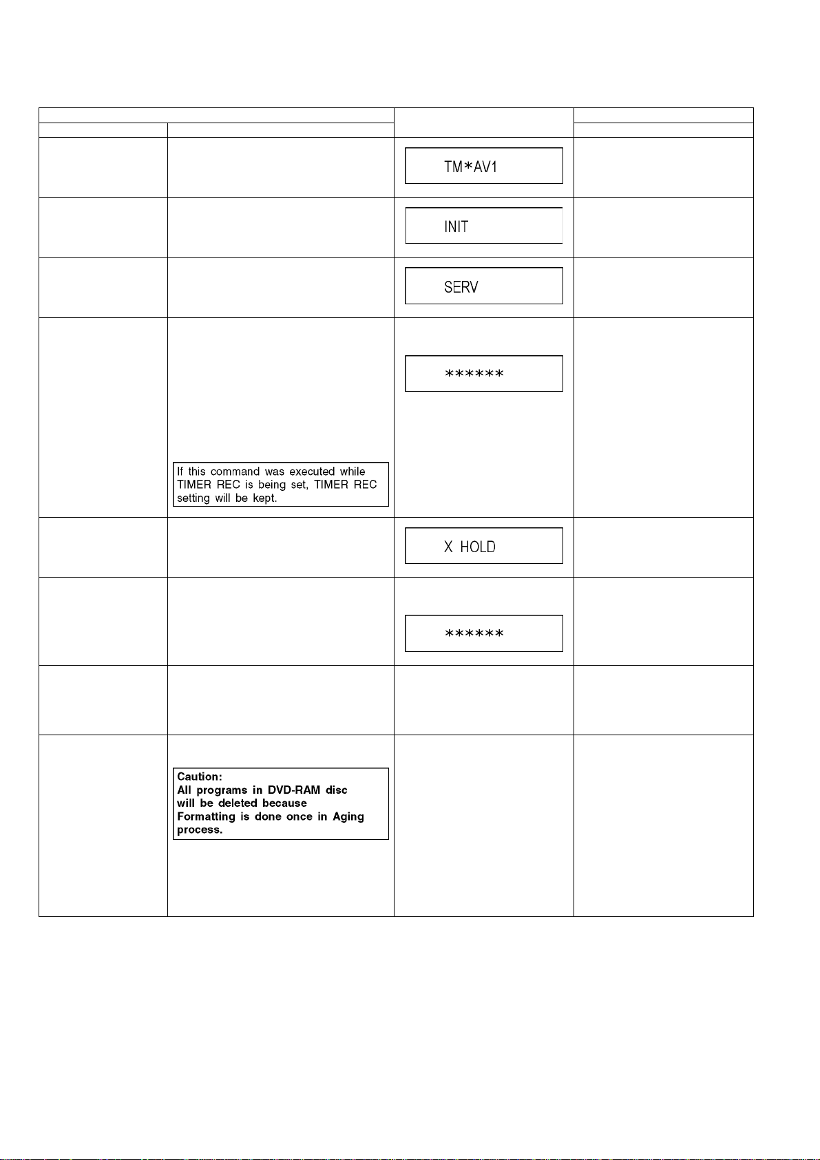
7.1.2. (DVD) Special Modes Setting
Item FL display Key operation
Mode name Description Front Key
TEST Mode *All the main unit's parameters (include tuner)
are initialized.
Rating password The audiovisual level setting password is ini-
tialized to “Level 8”.
Service Mode Setting every kind of modes for servicing.
*Details are described in “7.1.3. (DVD) Ser-
vice Mode at a glance”.
Forced disc eject Removing a disc that cannot be ejected.
The tray will open and unit will shift to P-off
mode.
*When Timer REC is ON or EXT-LINK is ON,
execute " Forced disc eject " after releasing
Timer REC or EXT-LINK.
*This command is not effective during "Child
lock" is ON.
While Demonstration Lock is being set, this
Forced disc eject function is not accepted.
The display before execution
leaves.
Press [VHS to DVD COPYING],
[REC] and [OPEN/CLOSE] keys
simultaneously for five seconds
when power is off.
Open the tray, set DRIVE SELECT
to DVD, and press [REC] and
[PLAY] simultaneously for 5 seconds.
When the power is off, press [VHS
to DVD COPYING], [OPEN/CLOSE]
and [STOP] keys simultaneously for
5 seconds.
When the power is off, press
[STOP] and [CH UP] keys simultaneously for 5 seconds.
Child lock/unlock Set or release “Child Lock”. Press [OK] and [RETURN] by
NTSC/PAL system select To switch PAL/NTSC alternately. The display before execution
Forced power-off Wh en the power button is not effective while
power is ON, turn off the power forcibly.
*When Timer REC is ON or EXT-LINK is ON,
execute “Forced Power-off” after releasing
Timer REC or EXT-LINK.
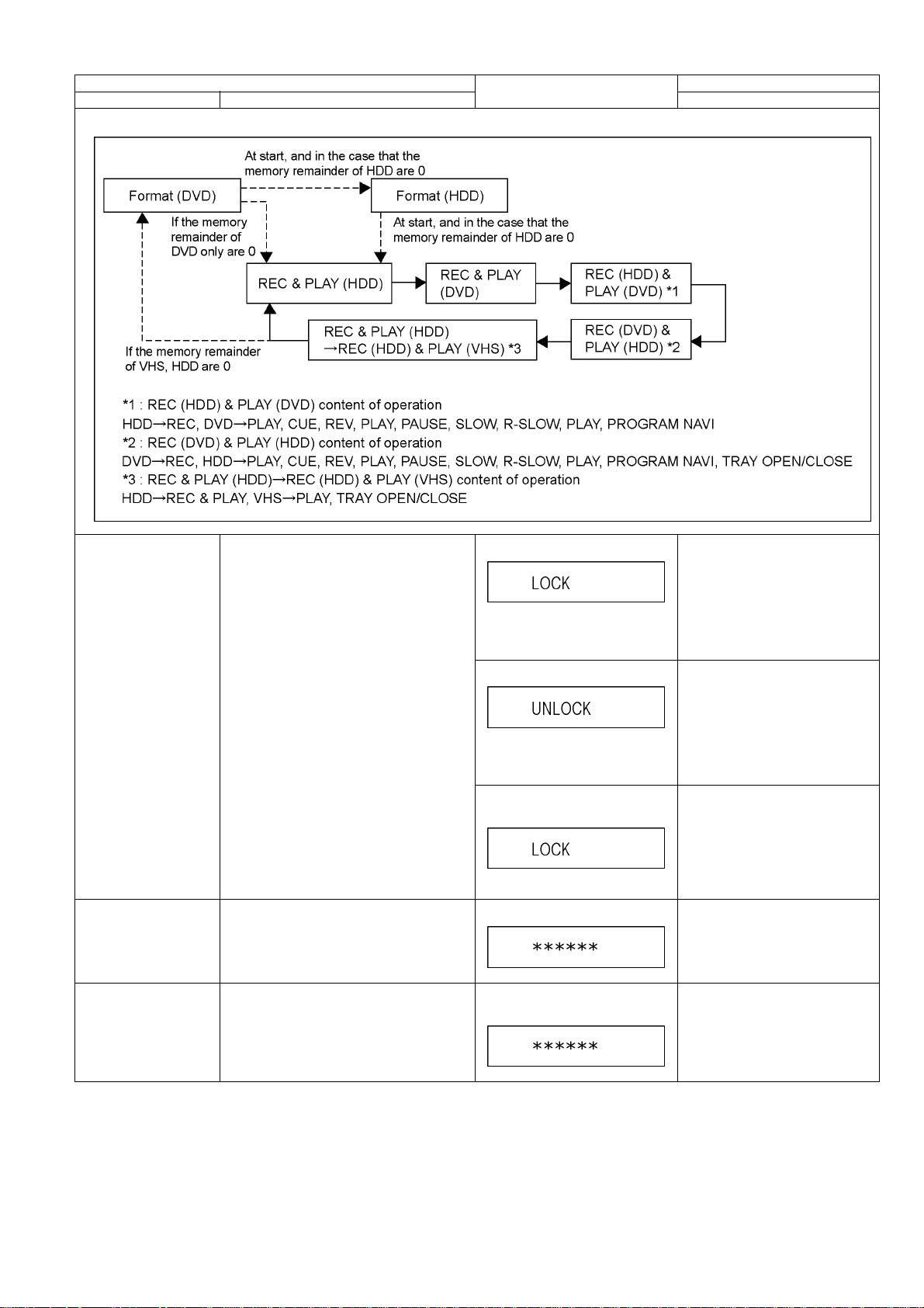
Aging Perform sequence of modes as * Aging
Description shown below continually.
leaves.
Display in P-off mode. Press [POWER] key over than 4
Display following the then mode. Set DRIVE SELECT to DVD.
remote controller simultaneously
until [X-HOLD] is displayed.
While the power is on (E-E mode),
press [STOP] and [OPEN/CLOSE]
simultaneously for 5 seconds.
seconds.
When the power is ON, press [CH
DOWN], [VHS to DVD COPYING]
and [OPEN/CLOSE] simultaneously for over 5 seconds and less
than 10 seconds.
Note:
If the unit has hung-up because of
pressing keys for over 10 seconds,
once turn off the power, and re-execute this command.
*When releasing Aging mode, press
[POWER] key, AC-OFF.
22
Page 23
Item FL display Key operation
Mode name Description Front Key
Aging Contents (Example):
Demonstration
lock/unlock
Ejection of the disc is prohibited.
The lock setting is effective until unlocking the
tray and not released by “Main unit initialization” of service mode.
*When lock the tray.
When the power is on, press
[STOP] and [POWER] keys simultaneously for 5 seconds in the condition that a disc in the tray.
Note:
“LOCK” is displayed for 3 seconds.
*When unlock the tray.
Time difference between pressing
[STOP] and [POWER] should be
within 0.5 sec.
When the power is on, press
[STOP] and [POWER] keys simultaneously for 5 seconds while the tray
being locked.
Note:
“UNLOCK” is displayed for 3 seconds.
*When press OPEN/CLOSE key
while the tray being locked.
Display “LOCK” for 3 seconds.
ATP re-execution Re-execute ATP. Display at ATP executing. When the power is on (E-E mode),
Progressive initialization The progressive setting is initialized to Inter-
lace.
The display before execution
leaves.
Time difference between pressing
[STOP] and [POWER] should be
within 0.5 sec.
Press [OPEN/CLOSE] key while the
tray being locked.
press [CH UP] and [CH DOWN]
simultaneously for 5 seconds.
When the power is on (E-E mode),
press [STOP] and [VHS to DVD
COPYING] simultaneously for 5
seconds.
23
Page 24
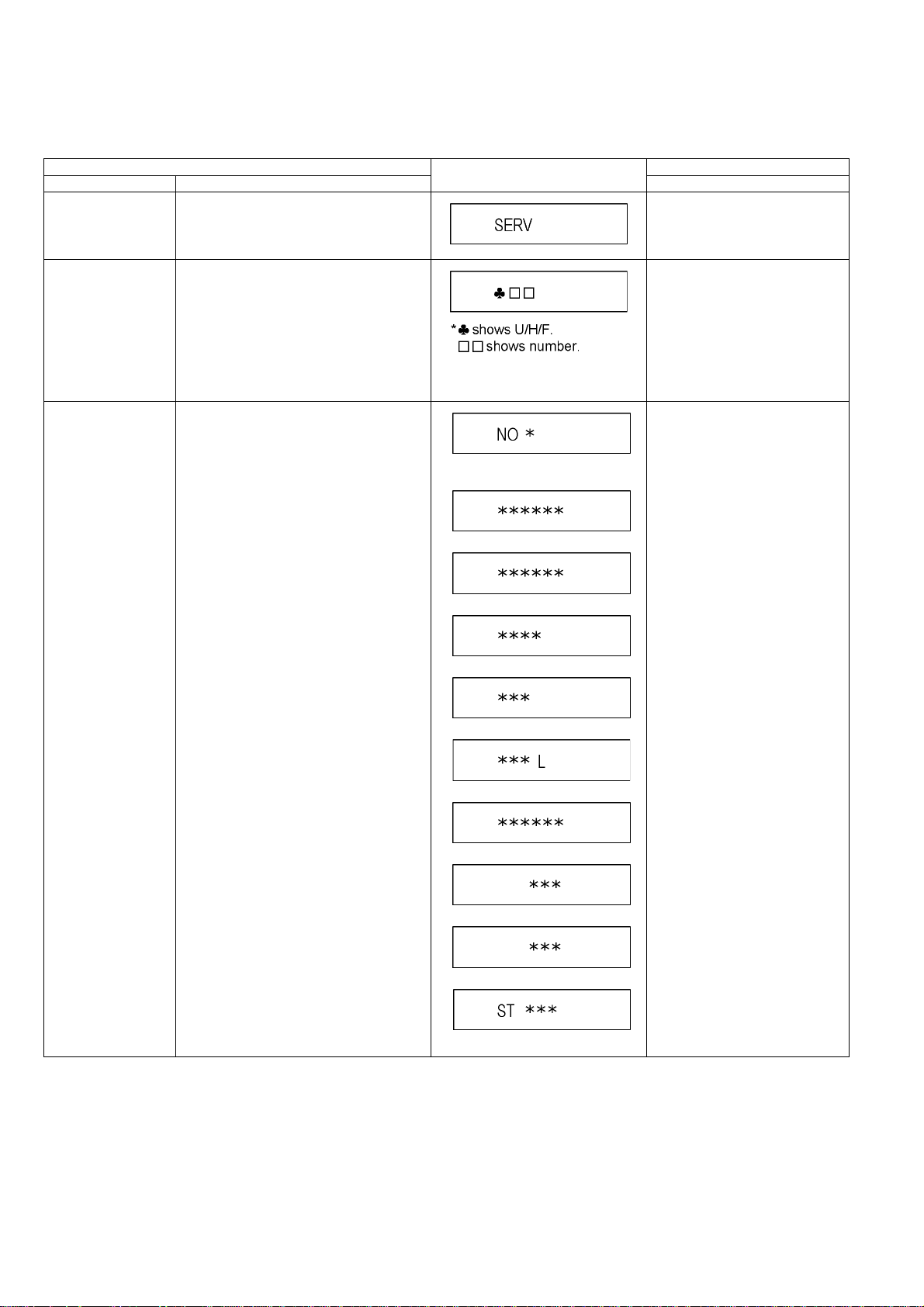
7.1.3. (DVD) Service Modes at a glance
Service mode setting: While the power is off, press [STOP], [VHS to DVD COPYING] and [OPEN / CLOSE] simultaneously for five
seconds.
Item FL display Key operation
Mode name Description (Remote controller key)
Release Items Item of Service Mode executing is cancelled. Press [0] [0] in service mode.
Error Code Display Last Error Code of U/H/F held by Timer is dis-
played on FL.
*Details are described in “7.1.1. (DVD) Self-
Diagnosis Functions”.
ROM Version Display 1. Region code (displayed for 5 sec.)
2. Main firm version (displayed for 5 sec.)
3. Timer firm version (displayed for 5 sec.)
4. Drive firm version (displayed for 5 sec.)
5. ROM correction version (displayed for 5
sec.)
6. VHS Microprocessor version
(displayed for 5 sec.)
7. VHS ROM correction version
(displayed for 5 sec.)
8. Boot 2 version (displayed for 5 sec.)
9. Boot 3 version (displayed for 5 sec.)
10. ST Microprocessor version (left displayed)
If any error history does not exist,
[F00] is displayed.
1.
*: Region of DVD (Example: 1,2.....)
2.
3.
4.
5.
Press [0] [1] in service mode.
Press [0] [2] in service mode.
6.
7.
8.
9.
10.
* are version displays.
24
Page 25
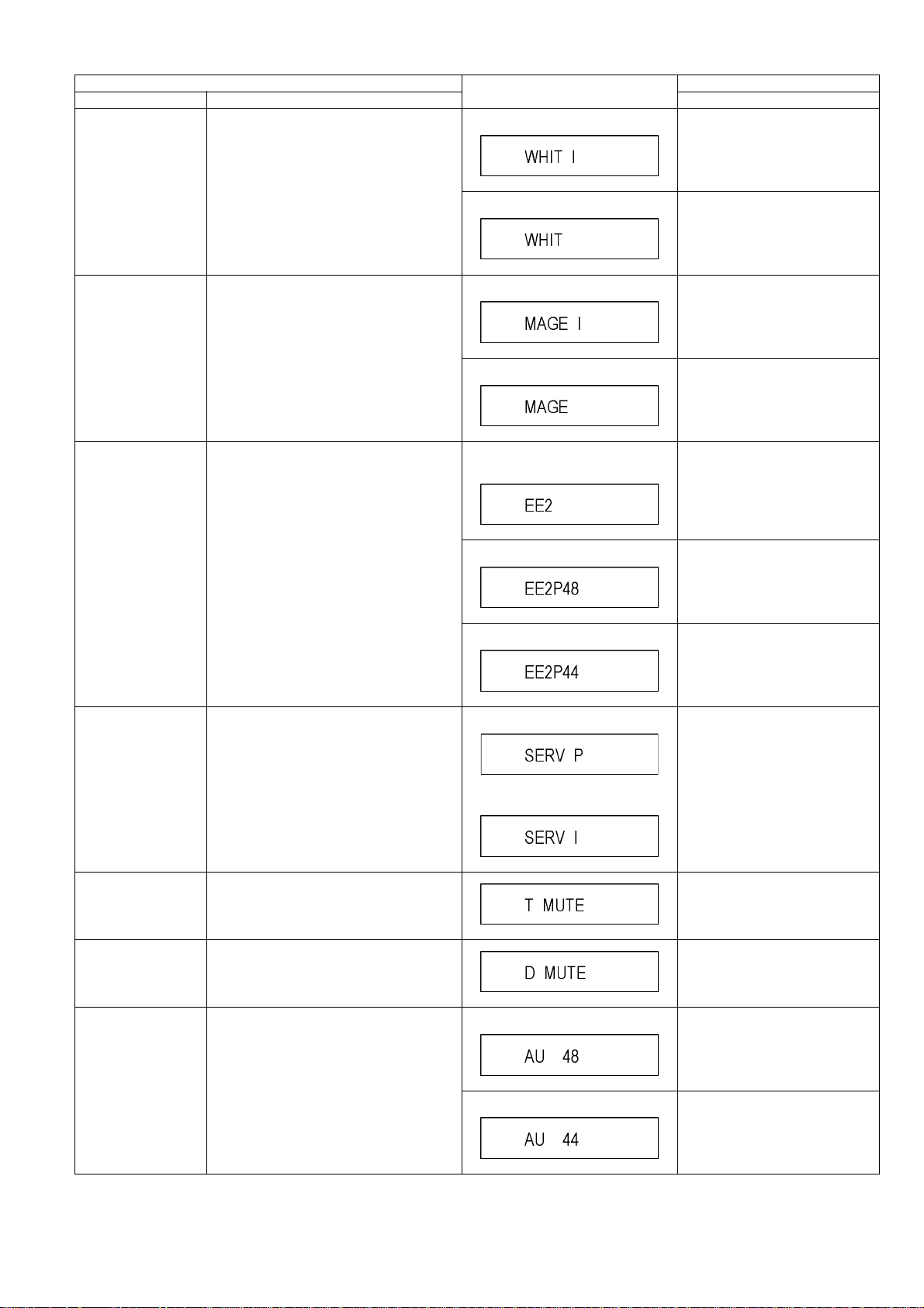
Item FL display Key operation
Mode name Description (Remote controller key)
White Picture Output White picture is output as component Output
from AV Decoder.
*White picture
(Saturation rate : 100%)
*It is enable to switch Interlace/Progressive
by “I/P switch: [1] [4]”
*Initial mode is “Interlace”. Press [1] [1] in service mode.
Switch Interlace/Progressive Press [1] [4] in White Picture Outpu t
mode.
*I/P are switched alternately.
Magenta Picture Output
RTSC Return in XP
(A & V)
I/P Switch Switch Interlace and Progressive in EE mode.
Magenta picture is output with Component
Output from AV Decoder.
*Magenta picture
(Saturation rate: 100%)
*It is enable to switch Interlace/Progressive
by “I/P switch: [1] [4]”
AV1 input signal is encoded (XP), decoded
(XP) and output decoded signal to external
without DISC recording and DISC playback.
*Initial setting is “Interlace”.
*This command is effective during executing
“White Picture Output”, “Magenta Picture Output” and “RTSC Return in XP (A & V)” modes.
*Initial mode is “Interlace”. Press [1] [2] in service mode.
Switch Interlace/Progressive Press [1] [4] in Magenta Picture
Output mode.
*I/P are switched alternately.
Initial mode: EE2/ Interlace/ XP/
Audio 48kHz
Switch Interlace/Progressive Press [1] [4] in RTSC Return XP
Audio 44.1 kHz/ 48 kHz Switch Press [2] [4] in RTSC Return XP
Initial mode is Interlace
Switch Interlace/Progressive
Press [1] [3] in service mode.
mode.
*I/P are switched alternately.
mode.
*48 kHz / 44.1 kHz are switched
alternately.
Press [1] [4] in I/P Switch mode.
*I/P are switched alternately.
Audio Mute (XTMUTE) Check whether mute is applied normally by
the timer microprocessor.
Audio Mute (XDMUTE) Check whether mute is applied normally by
the Digital P.C.B.
Audio Pattern Output The audio pattern stored in the internal mem-
ory is output
(Lch: 1kHz/-18dB)
(Rch: 400Hz/-18dB)
*Audio sound clock switching operation of
DAC can be confirmed by sub command [2]
[4].
Press [2] [1] in service mode.
Press [2] [2] in service mode.
Initial mode (Audio 48kHz) Press [2] [3] in service mode.
Audio 44.1kHz/48kHz switching Press [2] [4] in Audio Pattern Output
mode.
*48 kHz / 44.1 kHz are switched
alternately.
25
Page 26
Item FL display Key operation
Mode name Description (Remote controller key)
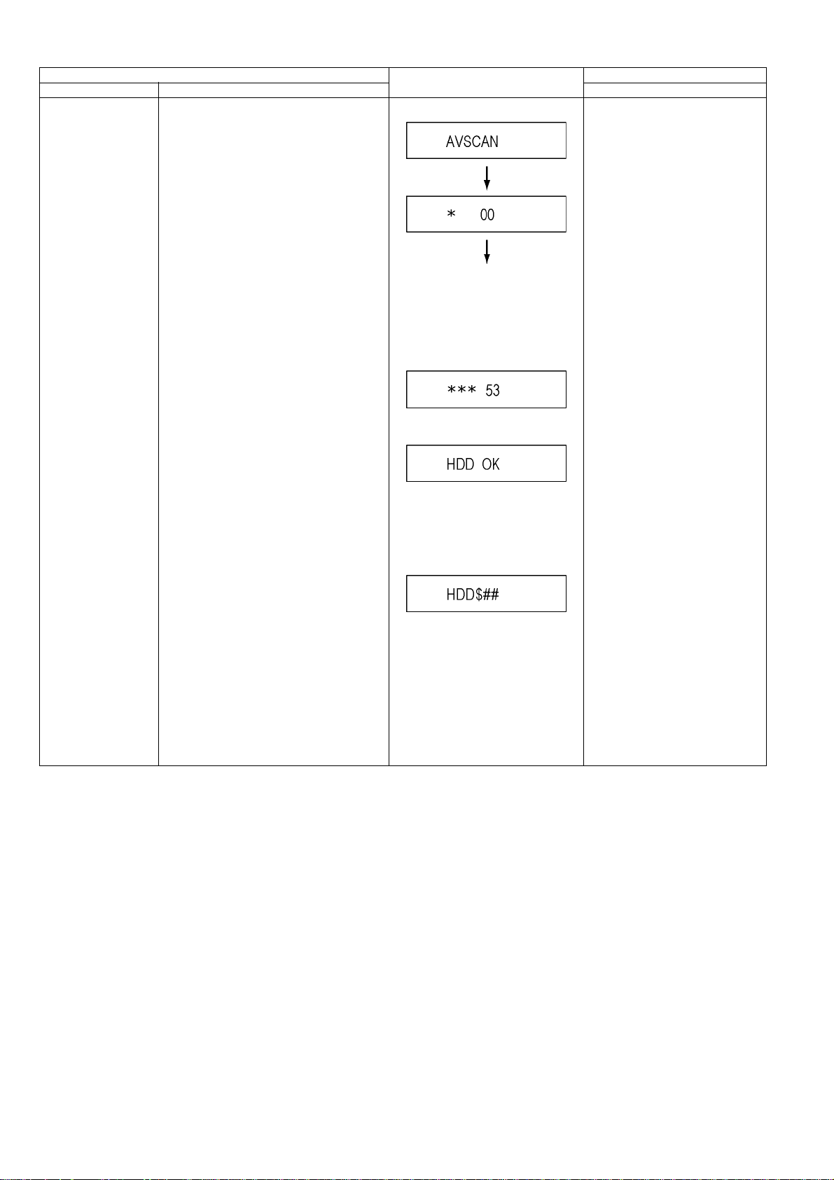
HDD READ SEEK
Inspection
Inspecting seek time of HDD to inspect performance.
At start
The [*] sign is added every 10 seconds while inspecting.
Two digits on the right side are the
progress level of the inspection (The
unit is %).
Example on the way of inspection:
When HDD is OK after inspection:
Press [3] [1] in service mode.
* When canceling the inspection
mode while executing, do “forced
power-off”.
Method:
Press [POWER] key more than 4
seconds.
(NG is displayed when error is excluding o)
(Transfer rate is calculated from the
AV scanning result, and when it is less
than 35Mbps, NG is displayed.)
$: [X] is displayed when seek time is
over 270msec., there is error or transfer rate is NG.
Position at $ is space when excluding
those.
##: Number of data of over 100msec.
and less than 270msec.
When it is over 100, [99] is displayed.
When the number is less than 5, we
judge it normal.
26
Page 27
Item FL display Key operation
Mode name Description (Remote controller key)
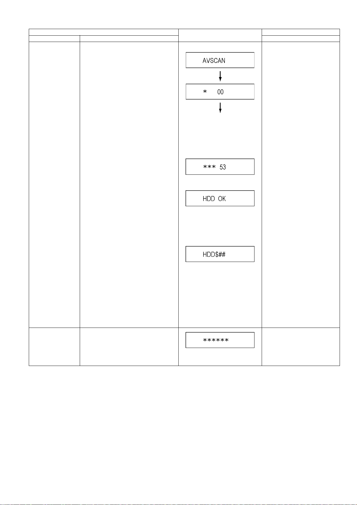
HDD READ VERIFY
Inspection
Measure of access time in READ VERIFY
MODE of HDD.
At start
The [*] sign is added every 10 seconds while inspecting.
Two digits on the right side are the
progress level of the inspection (The
unit is %).
Example on the way of inspection:
When HDD is OK after inspection:
Press [3] [2] in service mode.
* When canceling the inspection
mode while executing, do “forced
power-off”.
Method:
Press [POWER] key more than 4
seconds.
HDD Spin-up time The accumulation value of the Spin-up time of
HDD is displayed.
(NG is displayed when error is excluding o)
(Transfer rate is calculated from the
AV scanning result, and when it is less
than 35Mbps, NG is displayed.)
$: [X] is displayed when seek time is
over 270msec., there is error or transfer rate is NG.
Position at $ is space when excluding
those.
##: Number of data of over 100msec.
and less than 270msec.
When it is over 100, [99] is displayed.
When the number is less than 5, we
judge it normal.
Press [3] [3] in service mode.
Spin-up time of HDD is displayed.
(The unit of display is second.)
27
Page 28
Item FL display Key operation
Mode name Description (Remote controller key)
HDD Simple AV Scan Simple AV scan check of HDD
The [*] sign is added every 10 seconds while inspecting.
Two digits on the right side are the
progress level of the inspection (The
unit is %).
Example on the way of inspection:
When HDD is OK after inspection:
Press [3] [6] in service mode.
HDD Check Simple quality judgement of HDD
When HDD is NG after inspection:
[*] is the number of data of NG.
Press [3] [7] in service mode.
When HDD is OK:
When HDD is NG:
28
Page 29
Item FL display Key operation
Mode name Description (Remote controller key)
HDD/ DVD Drive Simple Check
Check if HDD Self-Diagnosis test was performed or Drive last error occurred within 4
weeks.
* If the current date or the date when the error
occurred is wrong, correct judgement may not
be made.
HDD Self-Diagnosis test start.
When HDD Self-Diagnosis test result
is OK.
When HDD Self-Diagnosis test result
is NG.
When the drive malfunction was
detected within 4 weeks ago.
When the drive malfunction was
detected more than 4 weeks ago or
Drive last error data does not exist.
Press [3] [8] in service mode.
Laser Used Time Indication
Delete the Laser Used
Time
Check laser used time (hours) of drive.
Laser used time stored in the memory of the
unit is deleted.
[HDD OK] from [DRV OK] are repeatedly displayed in turn.
Press [4] [1] in service mode.
• (*****) is the used time display in
hour.
• Laser used time of DVD/ CD in
Playback/Recording mode is
counted.
Press [9] [5] in service mode.
29
Page 30
Item FL display Key operation
Mode name Description (Remote controller key)
DVD Drive Last Error DVD Drive error code display.
*For details about the drive error code, refer
to the Service Manual for the specific DVD
Drive.
1. Error Number is displayed for 5 seconds.
2.The date when the error has
occurred is displayed for 5 seconds.
YY: Year
MM: Month
DD: Day
3. Last Drive Error (1/2) is displayed
for 5 seconds.
4. Last Drive Error (2/2) is displayed
for 5 seconds.
Press [4] [2] in service mode.
When “INFO******” is being displayed, past 19 error histories can
be displayed by pressing [0] [1] - [1]
[9]
Delete the Last Drive
Error
Laser power confirmation
Delete the Last Drive Error information stored
on the DVD Drive.
Drive state is judged based on difference
between laser power value at shipping and
present laser power value.
5. Error occurring Disc type is displayed for 5 seconds.
6. Disc Maker ID is displayed for 5
seconds.
7. Factor of Drive Error occurring is left
displayed
* is judgement result
In case that the maker cannot be
identified, display is black out.
Press [9] [6] in service mode.
1. into
DVD Drive in service mode.
(Other media are assumed to
be non-correspondence.)
2. Press [4] [4].
If DVD-RAM disc in not inserted, [NO
DISC] is displayed.
If power value study was filed,
[ERROR] is displayed.
30
Page 31

Item FL display Key operation
Mode name Description (Remote controller key)
Turn on all FL/LEDs All segments of FL and all LEDs are turned
on.
PB HIGH Signal Output
8 pin of AV 1 Jack (PB HIGH terminal) is High
(approx. 11V DC).
All segments are turned on. Press [5] [1] in service mode.
Press [5] [2] in service mode.
PB MIDDLE Signal
Output
Front connection
inspection
CEC (H) output Check of the CEC terminal high output of
CEC (L) output Check of the CEC terminal low output of
8 pin of AV 1 Jack (PB HIGH terminal) is Mid-
dle (approx. 5.5V DC)
Press all front keys and check the connection
between Main P.C.B. and Front key Switches.
HDMI.
HDMI.
(1) Each time a key is pressed, segment turned on increases one by one.
(2) Total umber of keys that have been
pressed.
When the check is OK.
When the check is NG.
When the check is OK.
Press [5] [3] in service mode.
Press [5] [4] in service mode.
Press [5] [5] in service mode.
Press [5] [6] in service mode.
Production Date Display
Display the accumulated working time
Display the date when the unit was produced.
Display the accumulated unit's working time.
When the check is NG.
Press [6] [1] in service mode.
YY: Year
MM: Month
DD: Day
Press [6] [4] in service mode.
(Indicating unit: Second)
31
Page 32

Item FL display Key operation
Mode name Description (Remote controller key)
Display the Error History
Display the Error History stored on the unit. Display reason of error for 5 seconds.
01:
Defect of Digital P.C.B.
(AV DEC / MAIN CPU)
02:
Defect of DVD Drive.
03:
Defect of Disc.
04:
Defect of Digital P.C.B. or Communication Error.
05:
Defect of Digital P.C.B.
(AV DEC / MAIN CPU)
06:
Defect of HDD.
Display the time when the error has
occurred for 5 seconds.
Press [6] [5] in service mode.
Then press [0] [1] ~ [9] [9], the past
99 error histories are displayed.
Delete the Error History
SD card WRITE check Delete Error History information stored on the
Delete Error History information stored on the
unit.
unit.
DD: Day
hh: Hour
mm: Minute
Accumulated working time till occurring of the error is left displayed.
(Indicating unit: Second)
When the WRITE check is OK.
When the WRITE check is NG.
*Note:
The image stored in the SD card will
be erased.
Press [9] [7] in service mode.
Insert a SD card to SD card slot,
and press [7] [4] in service mode.
*Insert SD card while the power is
off.
*Check for [CARD SD] display on
the FL display and go on the procedure.
32
Page 33

Item FL display Key operation
Mode name Description (Remote controller key)
USB check Display the volume label of the USB memory. When USB memory is not connected.
Press [7] [5] in service mode.
AV4(V)/AV1(RGB) I/O
Setting
AV2(Y/C)/AV1(V) I/O
Setting
AV2(V)/AV1(Y/C) I/O
Setting
Set input to AV4 (V) and set output to AV1
(RGB) for I/O checking
Set input to AV2 (Y/C) and set output to AV1
(V) for I/O checking
Set input to AV2 (V) and set output to AV1 (Y/
C) for I/O checking
When USB check is OK.
[*] is volume label.
Example of volume label is
[PANASONIC] :
When USB check is NG.
* Insert USB memory.
Press [8] [0] in service mode.
Press [8] [1] in service mode.
Press [8] [2] in service mode.
AV2(RGB)/AV1(V) I/O
Setting
P50(H) Output Timer Microprocessor IC9701-76 output High
P50(L) Output Timer Microprocessor IC9701-76 output Low
Tray OPEN/CLOSE
Test
Set input to AV2 (RGB) and set output to AV1
(V) for I/O checking
signal for AV1-pin 10 passing through inverter
(approx. 0V DC at AV1-pin 10).
signal for AV1-pin 10 passing through inverter
(approx. 4.4V DC at AV1-pin 10).
The tray is opened and closed repeatedly.
When the check is OK.
When the check is NG.
When the check is OK.
When the check is NG.
“*” is number of open/close cycle
times.
Press [8] [3] in service mode.
Press [8] [4] in service mode.
Press [8] [5] in service mode.
Press [9] [1] in service mode
*When releasing this mode, press
the [POWER] button of Remote
Controller more than 4 seconds.
33
Page 34

Item FL display Key operation
Mode name Description (Remote controller key)
Error code initialization Initialization of the last error code held by
timer (Write in F00)
Press [9] [8] in service mode.
Initialize Service Last Drive Error, Error history and Error
Codes stored on the unit are initialized to factory setting.
Finishing service mode Release Service Mode. Display in STOP (E-E) mode. Press power button on the front
Press [9] [9] in service mode.
panel or Remote controller in service mode.
34
Page 35

7.2. (VHS) Self-Diagnosis and Special Mode Setting
7.2.1. (VHS) Special Modes Setting
Note:
Set DRIVE SELECT to VHS.
Item FL display Key operation
Mode name Description Front Key
Tracking Center Tape Tracking is adjusted to center
FIX position.
VHS Service Mode In order to make service easy, a part
of inside information of a microprocessor is displayed on FIP.
*Details are described in “7.2.2.
(VHS) Service Mode”.
No display During PLAYBACK, press [CH UP]
and [CH DOWN] keys simultaneously.
Press [STOP], and [EJECT] keys
simultaneously for 3 seconds when
power is off.
Releasing EXT LINK and
Timer Program
Eject Ejecting Cassette Tape No display While in other than Timer REC mode,
Releasing Continuation EXT LINK
and Timer Program
No display While in EXT LINK and Timer REC
mode, press [STOP] key for 3 seconds.
press [STOP] key for 3 seconds or
press [STOP] key of the Remote Controller for 3 seconds.
35
Page 36

7.2.2. (VHS) Service Modes
1. Set DRIVE SELECT to VHS.
2. When power is off, press [STOP] and [EJECT] keys simultaneously for 3 seconds to into Service Mode.
3. In service mode, press [STOP] and [EJECT] keys simultaneously to add Service Number.
Service
Mode
Number
0 Indication for the
1 Indication for the
2 Indication for the
3 Self-diagnosis his-
4 Self-diagnosis his-
5 Self-diagnosis his-
6 Indication for the
7 Manual mecha-
Contents Contents of Indication on minute Contents of Indication on second Remarks
inner data of
IC6001
inner data of
IC6001
inner data of
IC6001
tory (1st)
tory (2nd)
tory (3rd)
inner data of
IC6001
nism operation
VHS mode
(Real time)
Tape beginning and ending detection
data (Real time)
00: Both tape beginning and ending
have not been detected
01: Tape ending is detecting now
02: Tape beginning is detecting now
03: Both tape beginning and ending
are detecting now
Mechanism position (Real time) Ordering for the Motors (Real time) The following functions are prohib0L: EJECT position
02: DOWN position
03: RREW position
04: LOAD position
05: REV position
06: PLAY position
07: POFF position
08: STOP_R position
09: STOP_F position
0 - : FF/REW position
0_ : Intermediate between each
positions
1st history of error number "- -" is displayed.
2nd history of error number "- -" is displayed
3rd history of error number "- -" is displayed
Servo data (4 digits)
(Real time)
Mechanism position (Real time) Ordering for the Motors Press the following key;
0L: EJECT position
02: DOWN position
03: RREW position
04: LOAD position
05: REV position
06: PLAY position
07: POFF position
08: STOP_R position
09: STOP_F position
0 - : FF/REW position
0 _: Intermediate between each
positions
Process number of the mechanism
movement
(Real time)
Key code
(Real time)
Indicate the receiving code when the
key of VCR or remote controller
being operated.
0*, 2*: CYL off,
CAP off
1*: CYL off,
CAP on (fwd)
3*: CYL off,
CAP on (rev)
8*, A*: CYL on,
CAP off
9*: CYL on,
CAP on (fwd)
B*: CYL on,
CAP on (rev)
*0: Motor off
*1: Loading
*2: Unloading
*3: Break (Load + Unload)
0*, 2*: CYL off,
CAP off
1*: CYL off,
CAP on (fwd)
3*: CYL off,
CAP on (rev)
8*, A*: CYL on,
CAP off
9*: CYL on,
CAP on (fwd)
B*: CYL on,
CAP on (rev)
*0: Motor off
*1: Loading
*2: Unloading
*3: Break (Load + Unload)
ited to operate the mechanism without cassette tape.
lTape beginning and ending detection.
lReel lock detection
lTape detection and tape position
detection
Press the EJET key for over 3 seconds in this mode, and then the VCR
is shifted into the special modes,
such as PG Adjustment, Model Code
Setting, and so on.
The orders for the motors are as follows.
PLAY key : Loading
STOP key : Unloading
36
Page 37

7.2.3. (VHS) Self-Diagnosis Functions
This model has a self-diagnosis. If the VHS section detects trouble during i nstallation or during use, the power is automatically
turned off or become power-save mode and it is memorized into the EEPROM (IC9705) as error code of two-digit number. It's memorized error code can be displayed in "second" display portion (the last 2 digits of the FIP) by placing the unit is Service Mode Number 2 when turning on Service Information Display as for example "01" or "02" etc as below. If a second error occurs, the most
recent error will be memorized and can be displayed in Service Mode Number 2. It can be memorized until 3 self-diagnosis histories
in maximum.
In order to erase the memorized error code, press STOP and EJECT buttons on the F ront Panel simultaneously over 5 seconds
during turning on Service Information Display mode.
7.2.3.1. Memory of the self-diagnosis history
*This is effective only in Service Mode 3, 4, 5.
7.2.3.1.1. Erro r Numbers at a glance
Memory No. (Error Code) Reason
01 The cylinder could not be started. (Error of the cylinder or the cylinder driver.)
02 The CAP FG could not be detected.
03 Mechanism lock during without the unloading and the cassette-up.
04 Mechanism lock during unloading
05 S-reel pulse cannot be detected during unloading. (Error of the S-reel circuit or the Capstan circuit)
06 Mechanism lock during the Cassette-up.
09 Communication error between VHS Microprocessor (IC6001) and Timer Microprocessor (IC9701).
15 S-reel pulse cannot be detected when a cassette tape is inserted.
(Error of the S-reel circuit or the Capstan circuit)
16 Detection of the Cylinder lock during the constant rotation
17 Detection of S-reel lock during the constant tape running
18 Detection of T-reel lock during the constant tape running
2*
Refer to following Note
80 An exceptional ejection depends on a accidental error
An error while the PG Automatic Adjustment
Note:
2* is as follows.
20 NG1 in the PG Shifter Automatic Adjustment (The cylinder rotation is unstable during the automatic adjustment.)
21 NG2 in the PG Shifter Automatic Adjustment (The vertical sync signal is lacked while over 5 seconds on the alignment tape.)
22 NG3 in the PG Shifter Automatic Adjustment (The installing position of Heads to the cylinder is our of specification.
23 NG4 in the PG Shifter Automatic Adjustment (The servo is not locked to the cylinder for more than 10 seconds)
7.2.3.1.2. Memory for the self-diagnosis history
1. The self-diagnosis result is memorized the state of the moment of detecting.
2. There are the histories from number 1 to number 3.
3. The latest error is memorized on history number 1, and then the old histories are shifted to the history number 2 and 3.
The error code memorized in the history number 2 and 3 is over-written by shift.
4. If the latest error is the same with the history number 1 (2nd-latest), it is not memorized.
(The same error code is not memorized in succession)
7.2.3.1.3. Clear for the self-diagnosis history
1. Press FF and EJECT buttons on the VCR simultaneously over 5 seconds during turning on Service Information Display mode.
37
Page 38

7.2.3.1.4. Indication of the self-diagnosis history.
The self-diagnosis histories can be indicated on the FIP with Service Mode number 3 to 5.
The procedure of service mode setting and indication format are the same as usual.
38
Page 39

8 Service Fixture & Tools
(For DVD)
Part Number Description Compatibility
RFKZ0168 Extension Cable (Digital IF P.C.B. - Fan Motor / 3 Pin) Same as EZ48V Series
VFK1729 Extension Cable (Digital IF P.C.B. - Main P.C.B. / 13 Pin) Same as EZ48V Series
RFKZ0216 Extension Cable (Main P.C.B. - Digital IF P.C.B. / 23 Pin / 40 mm) Same as EZ48V Series
RFKZ0240 Extension Cable (Main P.C.B. - Digital IF P.C.B. / 19 Pin / 40 mm×2) Same as EZ48V Series
RFKZ0215 Extension Cable (Main P.C.B. - Front Jack P.C.B. / 12 Pin) Same as EZ48V Series
RFKZ0169 Extension Cable (Digital IF P.C.B. - HDD / 4 Pin) Same as EH49 Series
RFKZ0260 Extension Cable (Digital IF P.C.B. - Digital P.C.B. / 88 Pin) Same as EZ48V Series
RFKZ0455 Extension Cable (Digital P.C.B. - HDD / 7 Pin) Same as EX795 Series
RFKZ03D01KS Lead Free Solder (0.3mm/100g Reel) Same as EZ48V Series
RFKZ06D01KS Lead Free Solder (0.6mm/100g Reel) Same as EZ48V Series
RFKZ10D01KS Lead Free Solder (1.0mm/100g Reel) Same as EZ48V Series
RFKZ0316 Solder Remover (Lead free low temperature Solder/50g) Same as EZ48V Series
RFKZ0328 Flux Same as EZ48V Series
(For VHS)
Part Number Description Compatibility
VFJ8125H3F PAL VHS Alignment Tape Same as EZ48V Series
VFK0329 Post Adjustment Screwdriver Same as EZ48V Series
VFK0330 Fine Adjustment Gear Driver Same as EZ48V Series
39
Page 40

9 Disassembly and Assembly Instructions
9.1. Disassembly Flow Chart
The following chart is the procedure for disassembling the casing and inside parts for internal inspection when carrying out the servicing.
To assemble the unit, reverse the steps shown in the chart below.
40
Page 41

9.2. P.C.B. Positions
41
Page 42

9.3. Caution with inserting cassette tape when disassembling the unit
Note1:
For description of the disassembling procedure, see the section 9.4.
Note2:
Video Cassette might not enter when a strong lighting is applied to VHS Mechanism when Video Cassette is inse rted. Please
weaken the lighting or cover with the top panel etc.
42
Page 43

9.4. Top Case
1. Remove 4 Screws (A) and 3 Screws (B).
2. Slide Top Case rearward and open th e both ends at rear
side of the Top Case a littl e and lift the Top Case in the
direction of the arrows.
3. Make the unit turn inside out, push the tabs (E) - (H) by
(-) screwdriver while pulling Front Panel in the direction of
arrow.
Note:
When attaching Front Panel, in order to hook Opener Lever
to Blinder Panel, push up Blinder Panel in the direction of
arrow and insert a Front Panel.
9.5. Front Panel
1. Remove one Screw (A).
2. Unlock 4 tabs in (A) - (D) turn.
43
Page 44

9.6. Front Jack P.C.B., FL Drive
P.C.B.
9.6.1. Front Jack P.C.B.
1. Remove 5 Tabs to remove Front Jack P.C.B.
9.6.2. FL Drive P.C.B.
1. Remove 3 Screws (A) and 2 Tabs to remove FL Drive
P.C.B.
2. Attach Tray Door in order from to .
: Put the Tray Door Spring on the Front Panel.
: Insert the shaft in the hole.
: Insert the shaft in the hole.
9.6.3. How to assemble Tray Door
1. Attach Tray Door Spring to T ray Door as following.
3. Confirm the Tray Door Spring is atta ched as following.
44
Page 45

9.6.4. Assembly of Blinder Panel and
Blinder Spring
Step 1: Insert Blinder Spring into shaft of Blinder Panel.
Step 3: Slide Blinder Panel into shaft hole of Front Panel.
Step 4: Slide down Blinder Panel to touch the shaft on top of
the rib.
Step 2: Hook Blinder Spring to bottom of the shaft.
Step 5: Press center of Blinder Panel and bow down.
Step 6: Push shaft into shaft hole.
45
Page 46

9.7. VHS Mechanism Unit
1. Disconnect 3 Connectors (P2501, P4002 and P6531).
2. Remove 3 Screws (A), Screw (B), Screw (C) and Screw
(D).
3. Lift up VHS Mechanism Unit perpendicularly so to disconnect Connectors (P2571 and P3001).
9.7.1. Caution for attaching VHS Mechanism Unit
1. Because Position SW should be set to "Eje ct Position",
refer to Fig.(A) and set the position switch so that the
boss and arrow mark come on a straight line.
2. Attach VHS Mechanism Unit so that Boss of Position SW
is put into long hole of Main Cam Gear, refer to Fig. (B).
Note:
Pay attention to stiff connections of P2571 and P4001,
when removing VHS Mechanism Unit.
46
Page 47

9.8. RAM/Digital P.C.B. Module
1. Remove the 3 Screws (A) to remove DVD Drive.
3. Remove 3 Screws (B) and 4 Connectors to remove the
Digital P.C.B.
4. Put Digital P.C.B. on DVD drive and remove RAM/Digital
P.C.B. Module.
2. Remove the Digital Barrier.
47
Page 48

Note:
RAM/Digital P.C.B. Module as service part has no Heat
Transfer Sheet.
Before returning to customer, Heat Transfer Sheet and
Sheet cover should be installed on Digital P.C.B.
9.9. SD/ USB P.C.B.
1. Remove 2 Screws (A) to remove USB Angle.
2. Make the USB Angle turn inside out.
Remove 2 Screws (B) to Remove SD/ USB P.C.B.
48
Page 49

9.10. Rear Panel, Fan Motor
9.10.1. Only Fan Motor
1. Disconnect Fan Connector.
2. Remove 2 Screws (A) to remove Fan Motor.
9.11. HDMI P.C.B.
1. Pull out the HDMI P.C.B. in the direction of arrow.
9.10.2. Rear Panel with Fan Motor
1. Disconnect Fan Connector.
2. Remove 8 Screws (B) and 2 Screws (C).
3. Unlock 2 Locking Tabs (A) to remove Rear Panel with
Fan Motor.
9.12. Digital IF P.C.B.
1. Remove 4 Screws (A) to remove DVD Angle.
49
Page 50

2. Disconnect 4 Connectors, HDD Power Cable and remove
2 Screws (B) to remove the Digital IF P.C.B.
9.13. HDD
1. Remove 2 Screws (A) on Rear Panel.
50
Page 51

2. Remove 3 Screws (B) and disconnect HDD Power Cable
and SATA Cable to remove HDD with HDD Bracket.
9.14. Backend P.C.B.
1. Pull out the Backend P.C.B. in the direction of arrows.
3. Put HDD up and down inversely so as not to give a shock
to HDD.
4. Remove 4 Screws (C) to remove HDD from HDD Bracket.
9.15. Main P.C.B.
1. Disconnect 4 Connectors.
2. Remove 2 Screws (A) and remove Main P.C.B.
51
Page 52

10 Measurements and Adjustments
10.1. Service Positions
Note:
For description of the disassembling procedure, see the section 9.
10.1.1. Checking and Repairing of Dig. Interface P.C.B.
52
Page 53

10.1.2. Checking and Repairing of Main P.C.B.
53
Page 54

10.1.3. Checking and Repairing of RAM/Digital P.C.B. Module
54
Page 55

10.1.4. Checking and Repairing of HDD
55
Page 56

10.2. Caution for Replacing Parts
10.2.1. Notice after replacing RAM/Digital P.C.B. Module
[TM AV1] is displayed, after replacing Digital P.C.B. or RAM/Digital P.C.B. Module.
Once power off, and start up again.
10.2.2. Items that should be done after replacing parts
*Note1:
Resetting object Condition of power Short Terminal
IC6001 POWER ON TL6004 (Reset L) and TL6002 (GND)
*Note2:
56
Page 57

*Note3:
Please prepare latest firmware updating disc.
* Main Firm is being recorded in HDD, but new HDD has no data.
Writing Procedure of Main Firm:
<<Caution>>
(1) Writing of Main Firm needs 3, 4 minutes.
(2) Never cut the power of DVD Recorder until writing in Firmware ends.
(3) Initial settings and contents of reservation will not change if writing is normally completed.
1. Prepare updating disc for firm ware.
2. Replace HDD.
3. Turn on power of DVD Recorder.
4. After [PLEASE WAIT] is displayed on FL., [HDD ERR] is displayed on FL.
5. Tray opens automatically.
6. Insert updating disc for Firmware and press OPEN/CLOSE key. (If a wrong disc was inserted, [NG DISK] [NO FVU] is displayed on FL.)
7. [LOAD] → [LD FVU] ←→ [M_FIRM] are displayed on FL alternately.
8. [MAIN] ←→ [UPD OK] blink alternately and Tray opens. Take out disc (Writing was finished).
9. Press Power button to turn off power.
10. Press Power button to turn on power.
1 1. [HELLO] → [SELF CHECK] are displayed on FL.
12. [UNFORMAT] is displayed on FL.
13. After [UNFORMAT] was displayed, message to request FORMAT is displayed on TV screen.
14. Select [Yes] and press [ENTER] key to format HDD.
(After FORMAT, program in HDD will be lost, but Main firm will not be lost.
“Write of the main farm" is completed above.
* Drive firm is not updated by above operation. If you wish update Drive firm, please prepare the disc for latest firmware update,
and write it again.
* If the version of the firm you have prepared was same as or later than that has already been written in deck, 'UNSUPPORT' is
displayed on FL.
* In a usual updating of firmware, writing is not performed when the timer reservation standby was not released.
57
Page 58

*Note4:
PG Shifter Automatic Adjustment Procedure
PROCEDURE F.I.P. DISPLAY
Turn on the Service Mode.
1. Set Drive Select to VHS and press the [STOP] and [EJECT] key simultaneously for more
than 3 seconds.
Activate the Service Mode 2. (Auto tracking will be turned off)
2. Press the [STOP] and [EJECT] key simultaneously twice.
Put it in PG adjustment mode.
3. Press the [EJECT] key for more than 3 seconds.
Set it adjustment No.1.
4. Press the [CH UP] key once.
Insert the alignment cassette tape (VFM8125H3F).
5. The PG Shifter Adjustment starts automatically.
6.This value displays that PG Adjustment data is memorized in EEPROM. For example:
Success Cassette tape is ejected automatically.
Result
NG1 in the PG Shifter Automatic Adjustment
(The cylinder rotation is unstable during the automatic
Error
Exit from Service Mode.
7. Press [STOP] and [EJECT] keys simultaneously in 6 times.
*Then the FIP becomes normal indication.
adjustment.)
NG2 in the PG Shifter Automatic Adjustment
(The vertical sync signal is lacked while over 5 seconds
on the alignment tape.)
NG3 in the PG Shifter Automatic Adjustment
(The installing position of Heads to the cylinder is out of
specification.)
NG4 in the PG Shifter Automatic Adjustment
(The servo is not locked to the cylinder for more than 10
seconds)
(Normal Indication)
58
Page 59

*Note5:
X-VALUE & LINEARITY (P2 and P3 Posts) Adjustment Procedure
1. Set the Auto Tracking to off.
(1) Set Drive Select to VHS and press the [STOP] and [EJECT] keys simultaneously for more than 3 seconds to enter Service
Mode.
(2) Press [STOP] and [EJECT] keys simultaneously twice to activate Service Mode 2, and then Auto-Tracking is turned off.
2. Perform the X-VALUE ADJUSTMENT
X-VALUE ADJUSTMENT
(1) After turning off the Auto tracking, playback the alignment Tape and press [CH UP] and [CH DOWN] keys simultaneously
to adjust the tracing to FIX value.
(2) Adjust A/C Head Base so that the envelope becomes maximum level.
(It is described on “5-2. Tape Interchangeability in “R4 Mechanism” that is separated volume.)
Alignment Tape VFM8125H3F
Test Point of Playback Envelope TW3001 (or TW4502)
LINEARITY ADJUSTMENT
(1) After turning off the Auto tracking, playback the alignment Tape and press [CH UP] and [CH DOWN] keys simultaneously
to adjust the tracing to FIX value.
(2) Adjust the LINEARITY so that the envelope is flat when moving tracking to (+) and (-) directions.
Alignment Tape VFM8125H3F
Test Point of Playback Envelope TW3001 (or TW4502)
l Main symptoms and Adjustment point
Envelope Post Name Adjustment Method
P2 Post Turn P2 Post counter-clockwise
P2 Post Turn P2 Post clockwise
P3 Post Turn P3 Post clockwise
P3 Post Turn P3 Post counter-clockwise
(Approx. 1/2 revolution)
(Approx. 1/4 revolution)
(Approx. 1/2 revolution)
(Approx. 1/4 revolution)
P2 Post P3 Post Turn P2 Post clockwise
(Less than 1 revolution)
Turn P3 Post counter-clockwise
(Less than 1 revolution)
59
Page 60

10.3. (DVD) St andard Inspection Specifications after Making Repairs
After making repairs, we recommend performing the following inspection, to check normal operation.
No. Procedure Item to Check
1 Turn on the power, and confirm items pointed out. Items pointed out should reappear.
2 Insert RAM disc. The Panasonic RAM disc should be recognized.
3 Enter the EE (TU IN / AV IN - AV OUT) mode. No abnormality should be seen in the picture, sound or operation.
4 Model with the HDD: Perform self-recor ding and playback for one
minute using the HDD.
5 Perform copy a progra m to disc and playback for one minute using
the RAM discs.
6 If a problem is caused by a VCD, DVD-R, DVD-Video, Audio-CD, or
MP3, playback the test disc.
7 Models with SD Card Slot, USB Input Jack or DV Input Jack: In
case of that the trouble is caused by SD Card and/or USB terminal
and/or DV terminal.
8 After checking and making repairs, upgrade the firmwar e to the lat-
est version.
9 Transfer [9][9] in the service mode setting, and initialize the service
settings (return various settings and error information to their
default values. The laser time is not included in this initialization).
No abnormality should be seen in the picture, sound or operation.
No abnormality should be seen in the picture, sound or operation.
*Panasonic DVD-RAM discs should be used when copying and
playback.
No abnormality should be seen in the picture, sound or operation.
Models with SD Card or USB Input Jack or DV Input Jack;
1) SD Card: Check to be able to display and copy the picture.
2) USB terminal: Check to be able to display and copy the picture.
3) DV terminal: Check to be able to record from DVC.
Make sure that [FIRM_SUCCESS] appears in the FL displays.
*[UNSUPPORT] display means the unit is already updated to newest same version. Then version up is not necessary.
Make sure that [CLR] appears in the FL display.
After checking it, turn the power off.
Use the following checklist to establish the judgement criteria for the picture and sound.
Item Contents Check Item Contents Check
Picture
Block noise
Crosscut noise Noise (static, background noise, etc.)
Dot noise The sound level is too low.
Picture disruption The sound level is too high.
Not bright enough The sound level changes.
Too bright
Flickering color
Color fading
Sound
Distorted sound
60
Page 61

61
Page 62

Table of contents
Service Manual
DSD1003007CE
Diagrams and Replacement
Parts List
Vol. 1
(K)...........Black Type
Colour
(S)...........Silver Type (only EX99VEG)
Model No.
DMR-EX99VEG
DMR-EX99VEB
DVD Recorder
Name of Signal
OFTR
FEP
This signal is connected
to the FEP schematic diagram.
Circuit name being connected.
6.Use the parts number indicated on the Replacement Parts List .
7.Indication on Schematic diagrams:
5.The voltage being indicated here may be include observational-error (deviation) due to
internal-resistance and/or reactance of equipment. Therefore, handle the value
indicated on here as reference.
4.Although the voltage and waveform available on here is measured with standard frame,
it may be differ from actual measurement due to modification of circuit and so on.
3.The voltage being indicated on the schematic diagram is measured in
"Standard-Playback" mode when there is no specify mode is mentioned.
2.It is only the "Test Round" and no terminal (Pin) is available on the P.C.B.
when the TP (Test Point) indicated as " " mark.
1.Although reference number of the parts is indicated on the P.C.B. drawing and/or
schematic diagrams, it is NOT mounted on the P.C.B. when it is displayed with "$" mark.
FOR SAFETY. WHEN REPLACING ANY OF THESE COMPONENTS USE ONLY THE SAME TYPE.
COMPONENTS IDENTIFIED WITH THE MARK HAVE THE SPECIAL CHARACTERISTICS
S1. About Indication of The Schematic Diagram
S1.1. Important Safety Notice
S1. About Indication of The Schematic Diagram ............................ S-1
S1.1. Important Safety Notice......................................................... S-1
S2. Voltage and Waveform Chart ................................................... S-2
S2.1. VHS_Main P.C.B. ..................................................................S-2
S2.2. SD_USB P.C.B. ..................................................................... S-4
S2.3. Digital_IF P.C.B. ....................................................................S-4
S2.4. FL_Drive P.C.B. ..................................................................... S-6
S3. Block Diagram .......................................................................... S-7
S3.1. Power Supply Block Diagram................................................ S-7
S3.2. Main P.C.B. Regulator Block Diagram ..................................S-8
S3.3. Analog Video Block Diagram ................................................. S-9
S3.3.1. Analog Video Block Diagram (1) ........................................S-9
S3.3.2. Analog Video Block Diagram (2) ......................................S-10
S3.4. Analog Audio Block Diagram ............................................... S-11
S3.4.1. Analog Audio Block Diagram (1) ...................................... S-11
S3.4.2. Analog Audio Block Diagram (2) ......................................S-12
S3.5. System Control & Servo Block Diagram .............................S-13
S3.6. Digital IF/Timer Block Diagram ...........................................S-14
S3.7. HDMI P.C.B. & SD/USB P.C.B. Block Diagram ................... S-15
S4. Schematic Diagram ................................................................ S-16
S4.1. Interconnection Diagram ..................................................... S-16
S4.1.1. Interconnection Diagram (1)............................................. S-16
S4.1.2. Interconnection Diagram (2)............................................. S-17
S4.2. Video (V) Schematic Diagram ............................................. S-18
S4.3. Audio (A) Schematic Diagram ............................................. S-22
S4.4. Syscon_Servo (S) Schematic Diagram ............................... S-24
S4.5. AV_IO (AV) Schematic Diagram .......................................... S-28
S4.6. Tuner (TU) Schematic Diagram .......................................... S-32
S4.7. Front_Jack Schematic Diagram .......................................... S-36
S4.8. SD_USB Schematic Diagram .............................................S-37
S4.9. HDMI Schematic Diagram................................................... S-38
S4.10. Power (P) Schematic Diagram .......................................... S-40
S4.11. D-IF (IF) Schematic Diagram ............................................ S-44
S4.12. FL_DCDC (FL) Schematic Diagram.................................. S-48
S4.13. FL_Drive Schematic Diagram ........................................... S-49
S5. Print Circuit Board .................................................................. S-50
S5.1. VHS_Main P.C.B. ................................................................S-50
S5.1.1. VHS_Main P.C.B. (Component Side) ............................... S-50
S5.1.2. VHS_Main P.C.B. (Foil Side) ............................................ S-54
S5.2. Front_Jack P.C.B. ...............................................................S-58
S5.3. SD_USB P.C.B. ................................................................... S-59
S5.3.1. SD_USB P.C.B. (Component Side) .................................. S-59
S5.3.2. SD_USB P.C.B. (Foil Side) ..............................................S-60
S5.4. HDMI P.C.B. ........................................................................S-61
S5.5. Digital_IF P.C.B. ..................................................................S-62
S5.5.1. Digital_IF P.C.B. (Component Side) ................................. S-62
S5.5.2. Digital_IF P.C.B. (Foil Side) .............................................. S-66
S5.6. FL_Drive P.C.B. ................................................................... S-70
S6. Abbreviation ........................................................................... S-75
S6.1. DVD Abbreviation Table ......................................................S-75
S6.2. VHS Abbreviation Table ...................................................... S-79
S7. Replacement Parts List .......................................................... S-88
S8. Exploded View .....................................................................S-103
S8.1. Frame and Casing Section (1) .......................................... S-103
S8.2. Frame and Casing Section (2) .......................................... S-104
S8.3. Mechanism Section ........................................................... S-105
S8.4. Packing Parts and Accessories Section ............................ S-106
S-1
Page 63

S2. Voltage and Waveform Chart
Note) Indicated voltage values are the standard values for the unit measured by the DC electronic circuit tester (high-impedance) with the chassis taken as standard.
Therefore, there may exist some errors in the voltage values, depending on the internal impedance of the DC circuit tester.
S2.1. VHS_Main P.C.B.
REF No.
IC2501 1 12.6 12.6 12.6
IC2501 2 0.1 0.1 0.1
IC2501 3 0 0 0
IC2501 4 0.1 0.1 0.1
IC2501 5 0 0 0
IC2501 6 0 0 0
IC2501 7 16.2 16.2 16.2
IC2501 8 0 0 0
IC2501 9 2.8 2.8 2.8
IC2501 10 1.6 1.6 1.6
IC2501 11 1.6 1.6 1.6
IC2501 12 0.6 0.6 0.6
IC2501 13 1.5 1.5 1.5
IC2501 14 2.4 2.4 2.4
IC2501 15 2.5 2.5 2.5
IC2501 16 2.5 2.5 2.5
IC2501 17 2.5 2.5 2.5
IC2501 18 1.3 1.3 1.3
IC2501 19 5 5 5
IC2501 20 3.6 3.6 3.8
IC2501 21 12.6 12.6 12.6
IC2501 22 3.6 3.6 3.8
IC2501 23 3.6 3.6 3.8
IC2501 24 0 0 0
IC2501 25 3.6 3.6 3.8
IC3001 1 1.7 1.7 1.7
IC3001 2 0 0 0
IC3001 3 0 0 0
IC3001 4 5.1 5.1 5.1
IC3001 5 2.1 2.1 2.1
IC3001 6 2.6 2.6 2.6
IC3001 7 2.8 2.8 2.8
IC3001 8 1.9 1.5 1.9
IC3001 9 1.8 1.4 1.8
IC3001 10 2.3 2.3 2.3
IC3001 11 2.6 2.6 2.6
IC3001 12 1.5 1.5 1.5
IC3001 13 0 0 0
IC3001 14 2.8 2.8 2.8
IC3001 15 2.7 2.7 2.7
IC3001 16 0 0 0
IC3001 17 2.7 2.7 2.7
IC3001 18 2 2 2
IC3001 19 2.7 2.7 2.7
IC3001 20 0 0 0
IC3001 21 2.7 2.7 2.7
IC3001 22 5 5 5
IC3001 23 2.3 2.3 2.3
IC3001 24 0 0 0
IC3001 25 2.1 2.1 2.1
IC3001 26 2.9 2.9 2.9
IC3001 27 0.4 0.4 0.4
IC3001 28 0 0 0
IC3001 29 2.4 2.4 2.4
IC3001 30 2.8 2.8 2.8
IC3001 31 0.4 0.4 0.4
IC3001 32 2.2 2.2 2.2
IC3001 33 2.1 2.1 2.1
IC3001 34 1.7 1.7 1.7
IC3001 35 3.1 3.1 3.1
IC3001 36 2.3 2.3 2.3
IC3001 37 3 3 3
IC3001 38 2.1 2.1 2.1
IC3001 39 1.5 1.5 1.5
IC3001 40 2.1 2.1 2.1
IC3001 41 2.5 2.5 2.5
PIN No.
REC PB EE
REF No.
IC3001 42 2 2 2
IC3001 43 2.1 2.1 2.1
IC3001 44 0 0
IC3001 45 3.2 3.2 3.2
IC3001 46 3.2 3.2 3.2
IC3001 47 5 5 5
IC3001 48 0.1 0.1 0.1
IC3001 49 0 3.1 3.1
IC3001 50 5 5 5
IC3001 51 1.9 1.9 1.9
IC3001 52 5 5 5
IC3001 53 2.6 2.6 2.6
IC3001 54 0 0 0
IC3001 55 1.9 1.9 1.9
IC3001 56 0 0 0
IC3001 57 2.2 2.2 2.2
IC3001 58 2.2 2.2 2.2
IC3001 59 5 5 5
IC3001 60 5 5 5
IC3001 61 4 4 4
IC3001 62 2.3 2.3 2.3
IC3001 63 2.2 2.2 2.2
IC3001 64 2.4 2.4 2.4
IC3001 65 2.2 2.2 2.2
IC3001 66 2.4 2.4 2.4
IC3001 67 2.2 2.2 2.2
IC3001 68 1.2 1.2 1.2
IC3001 69 2 2 2
IC3001 70 2.7 2.7 2.7
IC3001 71 2.2 2.2 2.2
IC3001 72 0.1 0.1 0.1
IC3001 73 4.3 4.3 4.3
IC3001 74 4.3 4.3 4.3
IC3001 75 2.8 2.8 2.8
IC3001 76 2.2 2.2 2.2
IC3001 77 - - IC3001 78 - - IC3001 79 0 0 0
IC3001 80 2.4 2.6 2.6
IC3001 81 0 0 0
IC3001 82 0 0 0
IC3001 83 3.2 3.2 3.2
IC3001 84 5 5 5
IC3001 85 2.4 2.4 2.4
IC3001 86 2.3 2.3 2.3
IC3001 87 2.4 2.4 2.4
IC3001 88 0 0 0
IC3001 89 2.3 0 0
IC3001 90 2.3 0 0
IC3001 91 2.3 0 0
IC3001 92 5.1 5.1 5.1
IC3001 93 0.6 0.6 0.6
IC3001 94 2.5 2.5 2.5
IC3001 95 2.5 2.5 2.5
IC3001 96 2.5 2.5 2.5
IC3001 97 0 0 0
IC3001 98 2.3 2.3 2.3
IC3001 99 0 0 0
IC3001 100 2.6 2.6 2.6
PIN No.
REC PB EE
<IC2501>
<IC3001>
REF No.
IC3002 1 5 5 5
IC3002 2 - - IC3002 3 1.3 1.3 1.3
IC3002 4 0 0 0
IC3002 5 4.6 4.6 4.6
IC3002 6 - - IC3002 7 - - IC3002 8 6.1 6.1 6.1
IC3901 1 2 2 2
IC3901 2 2.5 2.5 2.5
IC3901 3 1.6 1.6 1.6
IC3901 4 0 0 0
IC3901 5 1.6 1.6 1.6
IC3901 6 5 5 5
IC3901 7 1.6 1.6 1.6
IC3901 8 5 5 5
IC3901 9 0.4 0.4 0.4
IC3901 10 0.3 0.3 1.6
IC3901 11 1.6 1.6 1.6
IC3901 12 0.4 0.4 0.4
IC3901 13 0 0 0
IC3901 14 1.7 1.7 1.7
IC3901 15 1.7 1.7 1.7
IC3901 16 1.6 1.6 1.6
IC3901 17 0.4 0.4 0.4
IC3901 18 0 0 0
IC3901 19 0 0 0
IC3901 20 1.7 1.7 1.7
IC3901 21 0 0 0
IC3901 22 1.7 1.7 1.7
IC3901 23 1.7 1.6 1.6
IC3901 24 1.7 1.7 1.7
IC3901 25 5 5 5
IC3901 26 1.4 1.4 1.4
IC3901 27 0.1 0.1 0.2
IC3901 28 1.4 1.4 1.4
IC3901 29 0 0 0
IC3901 30 1.6 1.6 1.6
IC3901 31 1.6 1.6 1.6
IC3901 32 0 0 0
IC3901 33 1.6 1.6 1.6
IC3901 34 0 0 0
IC3901 35 2.1 2.1 2.1
IC3901 36 0 0 0
IC3901 37 1.6 1.6 1.6
IC3901 38 4.9 4.9 4.9
IC3901 39 1.6 1.6 1.6
IC3901 40 5 5 5
IC3901 41 1.6 1.6 1.6
IC3901 42 5 5 5
IC3901 43 2 2 2
IC3901 44 0 0 0
IC3901 45 2 2 2
IC3901 46 11.6 11.6 11.6
IC3901 47 1.6 1.6 1.6
IC3901 48 2 2 2
IC3901 49 4.5 4.5 4.5
IC3901 50 4.4 4.4 4.4
IC3901 51 4.4 4.4 4
IC3901 52 4 4 4.5
IC3901 53 4.5 4.5 4.5
IC3901 54 1.6 1.6 1.6
IC3901 55 4.5 4.5 4.5
IC3901 56 4.5 4.5 3.9
IC3901 57 9.1 9.1 9.1
IC3901 58 4.4 4.4 4
PIN No.
REC PB EE
REF No.
IC3901 59 4.4 4.4 4.2
IC3901 60 4.5 4.5 3.7
IC3901 61 4.5 4.5 3.7
IC3901 62 4.4 4.4 4.2
IC3901 63 4.5 4.5 3.7
IC3901 64 4.5 4.5 3.8
IC3901 65 9 9 9
IC3901 66 0 0 0
IC3901 67 0 0 0
IC3901 68 0 0 0
IC3901 69 0 0 0
IC3901 70 0 0 0
IC3901 71 4.5 4.5 4.5
IC3901 72 4.5 4.5 4.5
IC3901 73 4.5 4.5 4.5
IC3901 74 4.5 4.5 4.5
IC3901 75 0 0 0
IC3901 76 - - IC3901 77 9.5 9.5 0.3
IC3901 78 4.5 4.5 4.5
IC3901 79 4.5 4.5 4.5
IC3901 80 0 0 0
IC3901 81 2.1 2.1 2.1
IC3901 82 - - IC3901 83 1.5 1.5 1.5
IC3901 84 5 5 5
IC3901 85 2.1 2.1 2.1
IC3901 86 4.5 4.5 4.5
IC3901 87 3.6 3.6 3.6
IC3901 88 4.8 4.8 4.8
IC3901 89 4.6 4.6 4.6
IC3901 90 5 5 5
IC3901 91 2 2 2
IC3901 92 2.8 2.8 2.8
IC3901 93 2.1 2.1 2.1
IC3901 94 5 5 5
IC3901 95 2 2 2
IC3901 96 0 0 0
IC3901 97 2.1 2.1 2.1
IC3901 98 0 0 0
IC3901 99 2 2 2
IC3901 100 2.5 2.5 2.5
IC3905 1 0 0 0
IC3905 2 2.1 2.1 2.1
IC3905 3 5 5 5
IC3905 4 2 2 2
IC3905 5 0 0 0
IC3905 6 2.1 2.1 2.1
IC4501 1 - - IC4501 2 - - IC4501 3 - - IC4501 4 - - IC4501 5 - - IC4501 6 2.5 2.5 2.5
IC4501 7 2.5 2.5 2.5
IC4501 8 - - IC4501 9 0 0 0
IC4501 10 0 0 0
IC4501 11 0 0 0
IC4501 12 2.1 2.1 2.1
IC4501 13 0.1 0.1 0.1
IC4501 14 0.1 0.1 0.1
IC4501 15 0.1 0.1 0.1
IC4501 16 2.5 2.5 2.5
IC4501 17 0.5 0.5 0.5
IC4501 18 2.5 2.5 2.5
PIN No.
REC PB EE
S-2
Page 64

REF No.
IC4501 19 2.5 2.5 2.5
IC4501 20 2.1 2.1 2.1
IC4501 21 2.1 2.1 2.1
IC4501 22 2.1 2.1 2.1
IC4501 23 0 0 0
IC4501 24 2.1 2.1 2.1
IC4501 25 5 5 5
IC4501 26 2.1 2.1 2.1
IC4501 27 0 0 0
IC4501 28 4.3 4.3 4.3
IC4501 29 1.8 3.7 3.7
IC4501 30 1.8 3.7 3.7
IC4501 31 0 1.1 1.1
IC4501 32 2.5 2.5 2.5
IC4501 33 2.5 2.5 2.5
IC4501 34 0.8 0.8 0.8
IC4501 35 2.5 2.5 2.5
IC4501 36 0 0 0
IC4501 37 2.1 2.1 2.1
IC4501 38 0 0 0
IC4501 39 - - IC4501 40 5 5 5
IC4501 41 0 0 0
IC4501 42 4 4 4
IC4501 43 3.8 3.8 3.8
IC4501 44 3.2 3.2 3.2
IC4501 45 1.6 1.6 1.6
IC4501 46 4.9 4.9 4.9
IC4501 47 2.5 2.5 2.5
IC4501 48 2.5 2.5 2.5
IC4501 49 3.6 3.6 3.6
IC4501 50 - - IC4501 51 5 5 5
IC4501 52 0.1 0.1 0.1
IC4501 53 6 6 6
IC4501 54 - - IC4501 55 0 0 0
IC4501 56 0 0 0
IC4501 57 6 6 6
IC4501 58 12.1 12.1 12.1
IC4501 59 - - IC4501 60 0 0 0
IC4501 61 2.5 2.5 2.5
IC4501 62 2.5 2.5 2.5
IC4501 63 - - IC4501 64 - - IC6001 1 - - IC6001 2 0 0 0
IC6001 3 - - IC6001 4 0 0 0
IC6001 5 4.6 4.6 4.6
IC6001 6 4.6 4.6 4.6
IC6001 7 4.9 4.9 4.9
IC6001 8 4.9 4.9 4.9
IC6001 9 3.2 3.2 3.2
IC6001 10 4.9 4.9 4.9
IC6001 11 0 0 4.7
IC6001 12 1.3 1.3 1.3
IC6001 13 0 0 0
IC6001 14 4.9 4.9 4.9
IC6001 15 3.8 3.8 3.8
IC6001 16 - - IC6001 17 2.5 2.5 2.5
IC6001 18 2.4 2.4 0
IC6001 19 0 0 0
IC6001 20 0 4.8 4.8
PIN No.
REC PB EE
REF No.
IC6001 21 0 4.9 4.9
IC6001 22 0 0 0
IC6001 23 4.3 4.3 4.3
IC6001 24 - - IC6001 25 0 0 0
IC6001 26 0 0 0
IC6001 27 0 0 0
IC6001 28 0 0 0
IC6001 29 0 0 0
IC6001 30 0 0 0
IC6001 31 4.8 4.8 4.8
IC6001 32 4.8 4.8 4.8
IC6001 33 0 0 0
IC6001 34 4.9 4.9 4.9
IC6001 35 0 0 0
IC6001 36 0 0 0
IC6001 37 5 5 5
IC6001 38 - - IC6001 39 - - IC6001 40 0 0 0
IC6001 41 - - IC6001 42 - - IC6001 43 5 5 5
IC6001 44 - - IC6001 45 4.9 4.9 4.9
IC6001 46 0 0 0
IC6001 47 0 1.4 1.4
IC6001 48 2.1 2.1 2.1
IC6001 49 0 0 0
IC6001 50 1.7 1.7 1.7
IC6001 51 5 5 5
IC6001 52 1.7 1.7 1.7
IC6001 53 5 5 5
IC6001 54 2.1 2.1 2.1
IC6001 55 2.2 1.7 1.7
IC6001 56 2 2 2
IC6001 57 0 0 0
IC6001 58 4.9 4.9 4.9
IC6001 59 - - IC6001 60 - - IC6001 61 0 0 0
IC6001 62 0 0 0
IC6001 63 - - IC6001 64 - - IC6001 65 - - IC6001 66 - - IC6001 67 - - IC6001 68 4 4 4
IC6001 69 2.2 2.2 2.2
IC6001 70 4.2 4.2 4.2
IC6001 71 4.2 4.2 4.2
IC6001 72 4.1 4.1 4.1
IC6001 73 - - IC6001 74 0 0 0
IC6001 75 4.6 4.6 4.6
IC6001 76 2.5 2.5 0
IC6001 77 2.4 2.4 2.4
IC6001 78 - - IC6001 79 5 4.8 4.8
IC6001 80 4.5 0.2 0.2
IC6001 81 - - IC6001 82 0 0 0
IC6001 83 - - IC6001 84 - - IC6001 85 0 0 0
IC6001 86 2.6 2.6 2.6
PIN No.
REC PB EE
REF No.
IC6001 87 2.6 2.6 2.6
IC6001 88 0 0 0
IC6001 89 0 0 0
IC6001 90 1.3 1.3 1.3
IC6001 91 2.5 2.5 2.5
IC6001 92 2.5 2.5 2.5
IC6001 93 0 0 0
IC6001 94 2.5 2.3 2.3
IC6001 95 2.5 2.8 2.8
IC6001 96 2.5 2.5 2.5
IC6001 97 2.5 2.5 2.5
IC6001 98 5 5 5
IC6001 99 5 5 5
IC6001 100 3.3 3.3 3.3
IC6302 1 5 5 5
IC6302 2 0 0 0
IC6302 3 4.6 4.6 4.6
IC6302 4 6.1 6.1 6.1
IC6501 1 1.2 1.2 1.2
IC6501 2 2.4 2.4 2.4
IC6501 3 0.2 0.1 0.2
IC6501 4 0 0 0
IC6502 1 0 0 0
IC6502 2 1.2 1.2 1.2
IC6502 3 4.9 4.9 4.9
IC6502 4 0 0 0
IC7301 1 3.3 3.3 3.3
IC7301 2 1.7 1.7 1.7
IC7301 3 0 0 0
IC7301 4 1.7 1.7 1.7
IC7301 5 3.3 3.3 3.3
IC7301 6 3.3 3.3 3.3
IC7301 7 1.7 1.7 1.7
IC7301 8 0 0 0
IC7301 9 1.7 1.7 1.7
IC7301 10 3.3 3.3 3.3
IC7301 11 1.7 1.7 1.7
IC7301 12 1.7 1.7 1.7
IC7301 13 3.3 3.3 3.3
IC7301 14 1.3 1.3 1.3
IC7301 15 1.5 1.5 1.5
IC7301 16 1.3 1.3 1.3
IC7301 17 1 1 1
IC7301 18 1.3 1.3 1.3
IC7301 19 0 0 0
IC7301 20 3.3 3.3 3.3
IC7301 21 3.3 3.3 3.3
IC7301 22 0 0 0
IC7301 23 1.5 1.5 1.5
IC7301 24 0 0 0
IC7301 25 0 0 0
IC7301 26 1.5 1.5 1.5
IC7301 27 1.5 1.5 1.5
IC7301 28 3.3 3.3 3.3
IC7301 29 0 0 0
IC7301 30 1.5 1.5 1.5
IC7301 31 3.3 3.3 3.3
IC7301 32 4.2 4.2 4.2
IC7301 33 3.7 3.7 3.7
IC7301 34 3.3 3.3 3.3
IC7301 35 3.3 3.3 3.3
IC7301 36 0 0 0
IC7301 37 0 0 0
IC7301 38 0 0 0
IC7301 39 0 0 0
IC7301 40 0 0 0
PIN No.
REC PB EE
REF No.
IC7301 41 0 0 0
IC7301 42 0 0 0
IC7301 43 0 0 0
IC7301 44 0 0 0
IC7302 1 0 0 0
IC7302 2 0 0 0
IC7302 3 - - IC7302 4 3.3 3.3 3.3
IC7302 5 3.3 3.3 3.3
IC7304 1 3.3 3.3 3.3
IC7304 2 0 0 0
IC7304 3 4.8 4.8 4.8
IC7304 4 - - IC7304 5 1.5 1.5 1.5
IC7401 1 6.1 6.1 6.1
IC7401 2 0 0 0
IC7401 3 4.6 4.6 4.6
IC7401 4 - - IC7401 5 5 5 5
IC7402 1 6.1 6.1 6.1
IC7402 2 0 0 0
IC7402 3 4.9 4.9 4.9
IC7402 4 - - IC7402 5 5 5 5
IC7403 1 1.2 1.2 1.2
IC7403 2 0 0 0
IC7403 3 4.6 4.6 4.6
IC7403 4 6.1 6.1 6.1
IC7403 5 5 5 5
IC7801 1 6.1 6.1 6.1
IC7801 2 0 0 0
IC7801 3 4.6 4.6 4.6
IC7801 4 - - IC7801 5 5 5 5
P7401 1 5.6 5.6 5.6
P7401 2 0 0 0
P7401 3 5.6 5.6 5.6
P7401 4 0 0 0
P7401 5 0.2 0.2 0.2
P7401 6 0 0 0
P7401 7 0.4 0.4 0.4
P7401 8 2.4 2.4 2.4
P7401 9 0 0 0
P7401 10 0 0 0
P7401 11 0 0 0
P7402 1 3 3 3
P7402 2 3.8 3.8 3.8
P7402 3 1.7 1.7 1.7
P7402 4 3.1 3.1 3.1
P7402 5 3 3 3
P7402 6 3.2 3.2 3.2
P7402 7 3.2 3.2 3.2
P7402 8 0 0 0
P7402 9 11.6 11.6 11.6
P7402 10 0 0 0
P7402 11 - - Q3002 E 1.6 1.6 1.6
Q3002 C 5 5 5
Q3002 B 2.2 2.2 2.2
Q3901 E 5 5 5
Q3901 C 5 5 5
Q3901 B 4.3 4.3 4.3
Q4001 E -19.4 0 0
Q4001 C 10.4 0 0
Q4001 B -28.1 0.7 0.7
Q4002 E -19.4 0 0
PIN No.
REC PB EE
REF No.
Q4002 C 0 0 0
Q4002 B -28.1 0.7 0.7
Q4003 E 0 0 0
Q4003 C 5.1 0.3 0.3
Q4003 B -0.6 0.3 0.3
Q4004 E 6.1 6.1 6.1
Q4004 C 6 0.4 0.4
Q4004 B 5.4 6 6
Q4501 E 5 5 5
Q4501 C 6.1 6.1 6.1
Q4501 B 5.6 5.6 5.6
Q4502 E 12.2 12.2 12.2
Q4502 C 12.1 12.1 12.1
Q4502 B 11.7 11.7 11.7
Q4901 E 11.7 11.7 11.7
Q4901 C 11.6 11.6 11.6
Q4901 B 11 11 11
Q6102 E 1.6 1.6 1.6
Q6102 C 5 5 5
Q6102 B 2.2 2.2 2.2
Q6103 E 2.9 2.9 2.9
Q6103 C 5 5 5
Q6103 B 3.6 3.6 3.6
Q6104 E 2.2 2.2 2.2
Q6104 C 0 0 0
Q6104 B 1.6 1.6 1.6
Q6305 E 5 5 5
Q6305 C 6.1 6.1 6.1
Q6305 B 5.6 5.6 5.6
Q6501 E 0 0 0
Q6501 C 4.7 4.7 4.7
Q6502 E 0 0 0
Q6502 C 4.9 4.9 4.9
Q7802 E 0 0 0
Q7802 C 4.8 4.8 4.8
Q7802 B 0 0 0
Q7803 E 0 0 0
Q7803 C 0 0 0
Q7803 B 0.7 0.7 0.7
QR4004 E 5 5 5
QR4004 C -28.1 5 5
QR4004 B 4.8 0 0
QR4005 E 0 0 0
QR4005 C 0.1 6.1 6.1
QR4005 B 4.8 0 0
QR4501 E 0 0 0
QR4501 C 0 0 0
QR4501 B 4.6 4.6 4.6
QR4901 E 0 0 0
QR4901 C 0 0 0
QR4901 B 4.8 4.8 4.8
QR4911 E 4.7 4.7 4.7
QR4911 C 4.6 4.6 4.6
QR4911 B 0 0 0
QR4912 E 0 0 0
QR4912 C 0 0 0
QR4912 B 4.6 4.6 4.6
QR4913 E 0 0 0
QR4913 C 0 0 0
QR4913 B 4.6 4.6 4.6
PIN No.
REC PB EE
<IC6001>
S-3
Page 65

S2.2. SD_USB P.C.B.
S2.3. Digital_IF P.C.B.
REF No.
IC38002 1 0 0 3.3
IC38002 2 0 0 0
IC38002 3 3.3 3.3 3.3
IC38002 4 5 5 5
IC38002 5 5 5 0.3
PIN No.
REC PB EE
REF No.
IC9301 1 1.2 1.2 1.2
IC9301 2 0 0 0
IC9301 3 4.7 4.7 4.7
IC9301 4 6.1 6.1 6.1
IC9301 5 5 5 5
IC9700 1 1.7 1.7 1.7
IC9700 2 5 5 5
IC9700 3 0 0 0
IC9701 1 2.4 2.4 2.4
IC9701 2 4.3 4.3 4.3
IC9701 3 5 5 5
IC9701 4 4.7 4.7 4.7
IC9701 5 0.1 0.1 0.1
IC9701 6 - - IC9701 7 4.3 4.3 4.3
IC9701 8 0 0 0
IC9701 9 0 0 0
IC9701 10 0.8 0.8 0.8
IC9701 11 1.2 1.2 1.2
IC9701 12 4.6 4.6 4.6
IC9701 13 2 2 2
IC9701 14 0 0 0
IC9701 15 1.8 1.8 1.8
IC9701 16 3.3 3.3 3.3
IC9701 17 4.7 4.7 4.7
IC9701 18 3.3 3.3 3.3
IC9701 19 3.2 3.2 3.2
IC9701 20 0 0 0
IC9701 21 3 3 3
IC9701 22 1.3 1.3 0
IC9701 23 3.2 3.2 3.2
IC9701 24 - - IC9701 25 3.2 3.2 3.2
IC9701 26 3.2 3.2 3.2
IC9701 27 1.7 1.7 1.7
IC9701 28 3 3 3
IC9701 29 3.3 3.3 3.3
IC9701 30 3.3 3.3 3.3
IC9701 31 3.3 3.3 3.3
IC9701 32 3.3 3.3 3.3
IC9701 33 0 0 0
IC9701 34 - - IC9701 35 0.7 0.7 0.7
IC9701 36 3.2 3.2 3.2
IC9701 37 3.2 3.2 3.2
IC9701 38 3.3 3.3 3.3
IC9701 39 2.5 2.5 2.5
IC9701 40 4.8 4.8 4.8
IC9701 41 0 0 0
IC9701 42 4.6 4.6 4.6
IC9701 43 4.6 4.6 4.6
IC9701 44 4.7 4.7 4.7
IC9701 45 2.9 2.9 2.9
IC9701 46 4.7 4.7 4.7
IC9701 47 4.6 4.6 4.6
IC9701 48 0 0 0
IC9701 49 - - IC9701 50 0 0 0
IC9701 51 - - IC9701 52 - - IC9701 53 0 0 0
IC9701 54 0 0 0
IC9701 55 0 0 0
IC9701 56 0 0 0
IC9701 57 - - IC9701 58 - - -
PIN No.
REC PB EE
REF No.
IC9701 59 - - IC9701 60 5 5 5
IC9701 61 - - IC9701 62 4.7 4.7 4.7
IC9701 63 4.6 4.6 4.6
IC9701 64 0 0 0
IC9701 65 - - IC9701 66 0 0 0
IC9701 67 0 0 0
IC9701 68 0 0 0
IC9701 69 - - IC9701 70 - - IC9701 71 4.6 4.6 4.6
IC9701 72 - - IC9701 73 3.3 3.3 3.3
IC9701 74 4.9 4.9 4.9
IC9701 75 4.7 4.7 4.7
IC9701 76 0 0 0.1
IC9701 77 - - IC9701 78 0 0 0
IC9701 79 0 0 0
IC9701 80 3.9 3.9 3.9
IC9701 81 0 0 0
IC9701 82 3.3 3.3 3.3
IC9701 83 0 0 0
IC9701 84 2 2 2
IC9701 85 0 0 0
IC9701 86 4.7 4.7 4.7
IC9701 87 4.7 4.7 4.7
IC9701 88 4.7 4.7 4.7
IC9701 89 2 2 2
IC9701 90 4.7 4.7 4.7
IC9701 91 0 0 0
IC9701 92 0 0 0
IC9701 93 2.6 2.6 2.6
IC9701 94 1.6 1.6 1.6
IC9701 95 1.2 1.2 1.2
IC9701 96 0 0 0
IC9701 97 0 0 0
IC9701 98 1.8 1.2 1.9
IC9701 99 4.7 4.7 4.7
IC9701 100 4 4 4
IC9702 1 3.3 3.3 3.3
IC9702 2 3.3 3.3 3.3
IC9702 3 0 0 0
IC9702 4 - - IC9702 5 - - IC9703 1 4.9 4.9 4.9
IC9703 2 6.1 6.1 6.1
IC9703 3 0 0 0
IC9703 4 - - IC9703 5 - - IC9705 1 0 0 0
IC9705 2 0 0 0
IC9705 3 0 0 0
IC9705 4 0 0 0
IC9705 5 3.2 3.2 3.2
IC9705 6 3.2 3.2 3.2
IC9705 7 0 0 0
IC9705 8 3.3 3.3 3.3
IC9706 1 4.6 4.6 4.6
IC9706 2 4.7 4.7 4.7
IC9706 3 0 0 0
IC9706 4 0 0 0
IC9706 5 0 0 0
IC9707 1 4.8 4.8 4.8
PIN No.
REC PB EE
REF No.
IC9707 2 6.1 6.1 6.1
IC9707 3 0 0 0
IC9707 4 - - IC9707 5 - - IC9708 1 6.1 6.1 6.1
IC9708 2 0 0 0
IC9708 3 6 6 6
IC9708 4 - - -
IC9708 5 5 5 5
IC11150 1 2.2 2.2 2.2
IC11150 2 1.7 1.7 1.7
IC11150 3 0 0 0
IC11150 4 15 15 15
IC11150 5 0 0 0
IC11150 6 - - IC11150 7 - - IC11150 8 - - IC11150 9 - - -
IC11201 1 0 0 0
IC11201 2 0 0 0
IC11201 3 7.9 7.9 7.9
IC11201 4 2.5 2.5 2.5
IC11370 1 3.8 3.8 3.8
IC11370 2 6.1 6.1 6.1
IC11370 3 0 0 0
IC11370 4 5.1 5.1 5.1
IC11370 5 1.2 1.2 1.2
IC11700 1 12.4 12.4 12.4
IC11700 2 4.4 4.4 4.4
IC11700 3 1.1 1.1 1.1
IC11700 4 1 1 1
IC11700 5 1.1 1.1 1.1
IC11700 6 0 0 0
IC11700 7 8.8 8.8 8.8
IC11700 8 12.4 12.4 12.4
IC11750 1 3.8 3.8 3.8
IC11750 2 3.8 3.8 3.8
IC11750 3 3.3 3.3 3.3
IC11750 4 1.2 1.2 1.2
IC11750 5 0 0 0
IC14301 1 4.4 4.4 4.4
IC14301 2 4.6 4.6 4.6
IC14301 3 0 0 0
IC14301 4 1.2 1.2 1.2
IC14301 5 1.2 1.2 1.2
IC14301 6 0.6 0.6 0.6
IC14301 7 5.5 5.5 5.5
IC14301 8 5.4 5.4 5.4
IC14301 9 1.2 1.2 1.2
IC14301 10 0 0 0
IC14301 11 6 6 6
IC14301 12 4.4 4.4 4.4
IC14301 13 6.1 6.1 6.1
IC14301 14 7.4 7.4 7.4
IC14301 15 10.1 10.1 10.1
IC14301 16 12.4 12.4 12.4
PIN No.
REC PB EE
S-4
Page 66

REF No.
P9703 1 0 0 0
P9703 2 0 0 0
P9703 3 0 0 0
P9703 4 0 0 0
P9703 5 0 0 0
P9703 6 0 0 0
P9703 7 0 0 0
P9703 8 0 0 0
P9703 9 0 0 0
P9703 10 0 0 0
P9703 11 0 0 0
P9703 12 0 0 0
P9703 13 3 3 3
P9703 14 12.3 12.3 12.3
P9703 15 3.2 3.2 3.2
P9703 16 12.3 12.3 12.3
P9703 17 3.2 3.2 3.2
P9703 18 0 0 0
P9703 19 0.7 0.7 0.7
P9703 20 0 0 0
P9703 21 3.2 3.2 3.2
P9703 22 5 5 5
P9703 23 3.3 3.3 3.3
P9703 24 5 5 5
P9703 25 5 5 5
P9703 26 3.3 3.3 3.3
P9703 27 0 0 0
P9703 28 3.1 3.1 3.1
P9703 29 2.5 2.5 2.5
P9703 30 4.7 4.7 4.7
P9703 31 2.5 2.5 2.5
P9703 32 3.3 3.3 3.3
P9703 33 0 0 0
P9703 34 3.3 3.3 3.3
P9703 35 0 0 0
P9703 36 3.2 3.2 3.2
P9703 37 0 0 0
P9703 38 3.2 3.2 3.2
P9703 39 0 0 0
P9703 40 0 0 0
P9703 41 0 0 0
P9703 42 - - P9703 43 0 0 0
P9703 44 1.7 1.7 1.7
P9703 45 0 0 0
P9703 46 0 0 0
P9703 47 0 0 0
P9703 48 3.3 3.3 3.3
P9703 49 0 0 0
P9703 50 3.3 3.3 3.3
P9703 51 0.5 0.5 0.5
P9703 52 6.1 6.1 6.1
P9703 53 0 0 0
P9703 54 6.1 6.1 6.1
P9703 55 0.8 0.8 0.8
P9703 56 - - P9703 57 0 0 0
P9703 58 3.3 3.3 3.3
P9703 59 0.8 0.8 0.8
P9703 60 3.8 3.8 3.8
P9703 61 0 0 0
P9703 62 3.8 3.8 3.8
P9703 63 0.5 0.5 0.5
P9703 64 12.4 12.4 12.4
P9703 65 0 0 0
P9703 66 12.4 12.4 12.4
PIN No.
REC PB EE
REF No.
P9703 67 0.9 0.9 0.9
P9703 68 12.4 12.4 12.4
P9703 69 0 0 0
P9703 70 12.4 12.4 12.4
P9703 71 1.8 1.8 1.8
P9703 72 12.4 12.4 12.4
P9703 73 0 0 0
P9703 74 12.4 12.4 12.4
P9703 75 2.1 2.1 2.1
P9703 76 5 5 5
P9703 77 0 0 0
P9703 78 0 0 0
P9703 79 - - P9703 80 0 0 0
P9703 81 0 0 0
P9703 82 0 0 0
P9703 83 0 0 0
P9703 84 0.3 0.3 0.3
P9703 85 0 0 0
P9703 86 0 0 0
P9703 87 0 0 0
P9703 88 0 0 0
Q7702 E 12.4 12.4 12.4
Q7702 C -0.1 -0.1 -0.1
Q7702 B 12.3 12.3 12.3
Q7710 E 0 0 0
Q7710 C 36.2 36.2 36.2
Q7710 B -0.1 -0.1 -0.1
Q9106 E 3.3 3.3 3.3
Q9106 C 6.1 6.1 6.1
Q9106 B 3.9 3.9 3.9
Q9202 E 0 0 0
Q9202 C 4.7 4.7 4.7
Q9202 B 0 0 0.1
Q9203 E 0 0 0
Q9203 C 0 0 0
Q9203 B 1.8 1.8 1.8
Q9204 E 0 0 0
Q9204 C 4.7 4.7 4.7
Q9204 B 0 0 0
Q9701 E 2.7 2.7 2.7
Q9701 C 0 0 0
Q9701 B 2.1 2.1 2.1
Q9702 E 2 2 2
Q9702 C 5 5 5
Q9702 B 1.6 1.6 1.6
Q9703 E 1.1 1.1 1.1
Q9703 C 11.3 11.3 11.3
Q9703 B 1.6 1.6 1.6
Q9704 E 7.6 7.6 7.6
Q9704 C 12.4 12.4 12.4
Q9704 B 11.3 11.3 11.3
Q9705 E 0 0 0
Q9705 C 2.4 2.4 2.4
Q9705 B 1.8 1.8 1.8
Q9706 E 1.8 1.8 1.8
Q9706 C 5 5 5
Q9706 B 1.6 1.6 1.6
Q10101 E 0 0 0
Q10101 C 6.8 6.8 6.8
Q10101 B 0.1 0.1 0.1
Q10102 1 1.2 1.2 1.2
Q10102 2 0.1 0.1 0.1
Q10102 3 0 0 0
Q10102 4 0.1 0.1 0.1
Q11200 1 8.9 8.9 8.9
PIN No.
REC PB EE
REF No.
Q11200 2 7.9 7.9 7.9
Q11200 3 0 0 0
Q11200 4 1.7 1.7 1.7
Q11270 1 12.3 12.3 12.3
Q11270 2 12.3 12.3 12.3
Q11270 3 6.2 6.2 6.2
Q11270 4 12.4 12.4 12.4
Q11270 5 12.3 12.3 12.3
Q11270 6 12.3 12.3 12.3
Q11271 1 5 5 5
Q11271 2 5 5 5
Q11271 3 2.5 2.5 2.5
Q11271 4 5.1 5.1 5.1
Q11271 5 5 5 5
Q11271 6 5 5 5
Q11700 1 3.8 3.8 3.8
Q11700 2 3.8 3.8 3.8
Q11700 3 8.8 8.8 8.8
Q11700 4 12.4 12.4 12.4
Q11700 5 3.8 3.8 3.8
Q11700 6 3.8 3.8 3.8
Q14301 1 6.1 6.1 6.1
Q14301 2 6.1 6.1 6.1
Q14301 3 10.1 10.1 10.1
Q14301 4 12.4 12.4 12.4
Q14301 5 6.1 6.1 6.1
Q14301 6 6.1 6.1 6.1
Q14302 1 6.1 6.1 6.1
Q14302 2 6.1 6.1 6.1
Q14302 3 6 6 6
Q14302 4 0 0 0
Q14302 5 6.1 6.1 6.1
Q14302 6 6.1 6.1 6.1
QR7701 E 0 0 0
QR7701 C 12.3 12.3 12.3
QR7701 B 0 0 0
QR9101 E 0 0 0
QR9101 C 6 6 6
QR9101 B 0 0 0
QR9703 E 0 0 0
QR9703 C 0 0 0
QR9703 B 4.9 4.9 4.9
QR9705 E 3.2 3.2 3.2
QR9705 C 4.8 4.8 4.8
QR9705 B 3.3 3.3 3.3
QR9706 E 3.2 3.2 3.2
QR9706 C 4.8 4.8 4.8
QR9706 B 3.3 3.3 3.3
QR10103 E 0 0 0
QR10103 C 0 0 0
QR10103 B 4.6 4.6 4.6
QR11200 E 0 0 0
QR11200 C 0.1 0.1 0.1
QR11200 B 4.6 4.6 4.6
QR11270 E 0 0 0
QR11270 C 0 0 0
QR11270 B 4.6 4.6 4.6
QR11271 E 0 0 0
QR11271 C 0 0 0
QR11271 B 4.6 4.6 4.6
QR11700 E 0 0 0
QR11700 C 0 0 0
QR11700 B 4.6 4.6 4.6
QR11701 E 0 0 0
QR11701 C 4.4 4.4 4.4
QR11701 B 0 0 0
PIN No.
REC PB EE
REF No.
T11150 1 - - T11150 2 - - T11150 3 - - T11150 4 - - T11150 5 - - T11150 6 0 0 0
T11150 7 0 0 0
T11150 8 0 0 0
T11150 9 0 0 0
T11150 10 - - T11150 11 - - T11150 12 - - -
PIN No.
REC PB EE
<P9703> <T11150>
S-5
Page 67

S2.4. FL_Drive P.C.B.
REF No.
IC7501 1 0 0 0
IC7501 2 0 0 0
IC7501 3 0 0 0
IC7501 4 0 0 0
IC7501 5 2.8 2.8 2.8
IC7501 6 0.3 0.3 0.3
IC7501 7 0.3 0.3 0.3
IC7501 8 4.6 4.6 4.6
IC7501 9 4.2 4.2 4.2
IC7501 10 0.1 0.1 0.1
IC7501 11 0.1 0.1 0.1
IC7501 12 0 0 0
IC7501 13 4.7 4.7 4.7
IC7501 14 -17.8 -17.8 -20.7
IC7501 15 -17.8 -17.8 -20.7
IC7501 16 -9.3 -9.3 -20.7
IC7501 17 -17.8 -17.8 -17.9
IC7501 18 -20.7 -20.7 -20.7
IC7501 19 -17.9 -17.9 -20.7
IC7501 20 -6.5 -6.5 -20.7
IC7501 21 -15 -15 -17.9
IC7501 22 -0.1 -0.1 -15.1
IC7501 23 -9.4 -9.4 -12.2
IC7501 24 -9.4 -9.4 -20.7
IC7501 25 -17.9 -17.9 -20.7
IC7501 26 -20.7 -20.7 -20.7
IC7501 27 -20.7 -20.7 -20.7
IC7501 28 -20.7 -20.7 -20.7
IC7501 29 -12.2 -12.2 -20.8
IC7501 30 -21.4 -21.4 -21.4
IC7501 31 - - IC7501 32 - - IC7501 33 - - IC7501 34 - - IC7501 35 - - IC7501 36 -18.4 -18.4 -18.4
IC7501 37 -18.1 -18.1 -18.1
IC7501 38 -18.1 -18.1 -18.1
IC7501 39 -18.1 -18.1 -18.1
IC7501 40 -18.1 -18.1 -18.1
IC7501 41 -18.1 -18.1 -18.1
IC7501 42 -18.1 -18.1 -18.1
IC7501 43 4.7 4.7 4.7
IC7501 44 0 0 0
Q7502 E -18.5 -18.5 -18.5
Q7502 C 4.7 4.7 4.7
Q7502 B -18.4 -18.4 -18.4
QR7502 E 0 0 0
QR7502 C 0 0 0
QR7502 B 4.6 4.6 4.6
QR7503 E 0 0 0
QR7503 C 5.1 5.1 5.1
QR7503 B 0 0 0
QR7504 E 0 0 0
QR7504 C 5.1 5.1 5.1
QR7504 B 0 0 0
PIN No.
REC PB EE
S-6
Page 68

44
IC9701-
H
DI P ON
47
IC9701-
L
HDD_PFAIL
IC9701 40
L
DR_P_ON
IC9701 42
H
T11150
D11270
P9101 P6001
13,15
X_SW_5R8V
QR11700,QR11701
SW
1
IP9102
2
4
A
IC11201
3
K R
2
1
2
4
3
Q11200
D11152 D11156
D11151
D10102
B2
B1
P2
P1
9
21 3
10
6
5
3
1
DMR-EX99VEG/EB
Power Supply Block Diagram
1
2
4
3
Q10102
QR11200
Q10101
QR11270
sw
QR10103
VCC
4
4
1
3
2
GND
3
HOT COLD
IC11150
F/B
E/OCL 5
2
Z/C
D11101
VA11110, L11120
L11121
F11101
SURGE
SUPPRESSOR
AND
SURGE
ABSORBER
RECTFIER
SW TRANSFORMER
REG. D+12V
REG. D+5.8V
REG. AU+5.8V
REG. D+5.8V
REG. D+3.8V
REG. BE+3.8V
FROM
DIGITAL IF P.C.B.
TIMER SECTION
S_P_SAVE
TO
DIGITAL IF P.C.B.
TIMER SECTION
TO
DIGITAL P.C.B.
TO
DIGITAL P.C.B.
TO
DIGITAL P.C.B.
TO
DIGITAL IF P.C.B.
TIMER SECTION
FROM
DIGITAL IF P.C.B.
TIMER SECTION
TO
DIGITAL P.C.B.
TO
MAIN P.C.B.
TO
MAIN P.C.B.
TO
MAIN P.C.B.
(DC-DC CONVERTER)
(DC-DC
CONVERTER)
(DC-DC CONVERTER)
(ERROR VOLTAGE DETECTOR)
POWER ON/OFF
CONTROLER
(FEED BACK)
(FEED BACK)
(SWITCHING IC)
1
P11101
AC SOCKET
MECHA +12.5V
P9103 P6003
12
X_SW_12V
HDD_DR5V
HDD_DR5V
DR12V
DR12V
DR12V
P9703 P59001
64,66,68,70,72,74
P9707
1
TO HDD
P9707
4
P9703 P59001
14, 16
QR11271
HDD 5V
CONTROLER
ON:
H
P9703 P59001
25
AU +5V
3
V OUT 54
IC9301
V IN
P9104 P6004
8,9,10
BE +3.3V
X SW +5.8V
V OUT1 3
IC11750
V IN
34 S
D
D
G
D
D
25
16
Q11700
IC14301
43
S
D
D
G
D
D
52
61
Q14301
61
S
D
D
G
D
D
52
43
Q14302
61 S
EXTLO
EXT UP
VIN
SEL
SYNC
LX
FB
RS+
RS-
D
D
G
D
D
52
43
Q11270
71 VIN
CS
EXT
FB
5
8
V5
IC11700
D +3.8V
P9703 P59001
60,62
2
REG. D+5V
G
3
4
Q11271
S
D
D
D
D
25
1
6
42
IC11370
VIN VOUT
SENSE
ON 51
2
OSC
9
13
16
15
11
6
7
8
VCC
IC9707
(REG. +5V)
2
VOUT
1
DIGITAL IF P.C.B.
S3. Block Diagram
S3.1. Power Supply Block Diagram
S-7
Page 69

EXTCTL4
IC3901-
38
H
EXTCTL3
IC3901-
36
H
POWER ON
IC6001-
75
H
BIAS
IC6001-
21
H
H
13,15
P6001
MECHA +12.5V
X SW +5.8V
P9101
11,12
P6004P9104
X SW +12V
12
P6003P9103
BE +3.3V
8,9,10
P6004P9104
AD +5V AD +5V
2
P6001P9101
1
P2571
Q4004
(POWER SUPPLY)
Q4501,D4502
QR4005
( : ON)
:ON
H
:ON
3
V OUT
+5V
+5V
2
P2571
MECHA +12.5V
14
IC6302
(REG. +5 V )
V IN
GND
2
V OUT 5
1
IC7401
(REG. BOOSTER +5V)
V IN
CONT
H
19
TO
IC2501-
CONT
5
V OUT
REG.A +5V
OSD +5V
FROM
SYSTEM CONTROL &
SERVO SECTION
FROM
SYSTEM CONTROL &
SERVO SECTION
TO
CAPSTAN MOTOR
OSC BIAS
18
IC3002
(REG. OSD +5 V )
V IN
22
TO
IC3001-
,47,
50
60,84,92
,52,
53
IC6001-
PS +11.6V
46
TO
IC3901-
TO
U/VTUNER
1 21,
TO
IC2501-
42 84 94, ,
TO
IC3901-
6 8 25 40,,, ,
TO
IC3901-
37 99
TO
IC6001-
3
IC3905-
TO
U/VTUNER
6
TO
T4001-
Q4502
(POWER SUPPLY)
QR4501
( : ON)
H
Q4901
( POWER SUPPLY )
QR4901
(
H ON )
+12V
58
TO
IC4501-
+5.8VX_SW_5R8V
6,7
PS90002P7402
TO
Backend P.C.B.
TO
FRONT JACK P.C.B.
IC7601 -
BE +3.3V
11
PP4801PS6002
25 40,
TO
IC4501-
Q6305,D6306
REG. +5V
V REG +5V
98
TO
IC6001-
FROM
DIGITAL IF P.C.B.
3
GND2CONT
3
V OUT 5
1
IC7402
(REG. PS +5V)
V IN
GND
2 3
V OUT 5
4
IC7403
(REG. +5V)
V IN
3
DMR-EX99VEG/EB
MAIN P.C.B
Regulator Block Diagram
MAIN P.C.B.
S3.2. Main P.C.B. Regulator Block Diagram
S-8
Page 70

+
BIAS
CLAMP
BUFFER
AMP
48
47
VHS V Y OUT
FROM
SYSTEM
CONTROL &
SERVO
SECTION
FROM
Backend P.C.B.
DT_C
DT_Y
(SW17C)
a
b
(SW17V)
a
b
(SW17Y)
a
b
V/Y IN DM
CPN C IN DM
1.0V
2.3V
5V
:PB SIGNAL:REC SIGNAL
CLAMP
TUNER V
V OUT
30
RED/C15
VIDEO/Y19
GREEN11
(TV)
AV1
BLUE7
21PIN JACK
JK3901
OUT
VIDEO OUT
JK4901
1
4
(DECORDER TEXT)
AV2
VIDEO19
21PIN JACK
JK3902
DIGITAL P.C.B.
TO
P59001P9703
71
75
P9703 P59001
10
PP4801 PS6002
5
PS9001 P7401
7
PS9001 P7401
8
PP4801 PS6002
3
PP4801 PS6002
P59001P9703
83
88
P9703 P59001
P59001P9703
84
87
P9703 P59001
P9103P6003
2
1
P6003 P9103
P9102P6002
19
17
P6002 P9102
P9102P6002
16
P9102P6002
8
18
P6002 P9102
LOGIC
IIC BUS
SDA
89
SCL
88
FROM/TO
DIGITAL IF PCB
TIMER SECTION
FROM/TO
SYSTEM CONTROL &
SERVO SECTION
IIC DATA
IC9701-26
25IC9701-9TU7801-
9
TU7801-
FROM
MAIN P.C.B.
TUNER
SECTION
17TU7801-
IIC CLK
52IC6001-
C V OUT
(SW10)
CLAMP
CLAMP
CLAMP
CLAMP
BIAS
CLAMP
SLICER
85
OUT
ADC
V/Y
83
OUT
C-ADC
81
TUNER V
AV2 V/Y
AV2 R/C
AV3 V
AV3 C
AV3Y
AV1 V
CIRCUIT
SWITCH
SELECT
OUTPUT
ADC
OUT
V
AV2
28
SV2
e
d
c
b
a
OUT
V/Y/C
AV1
26
SV1
e
d
c
b
a
a
b
(SW9)
OUT
V
24
23
a
b
(SW8)
OUT
C
22
(SW7)
a
b
OUT
Y
20
19
OUT
G
AV1
17
6MHz
(SW5)
12MHz
a
b
c
15
OUT
Y
COMP
14
(SW6)
a
b
c
d
OUT
B
AV1
12
OUT
B-Y
COMP
11
6MHz
(SW4)
12MHz
a
b
c
d
OUT
R-C
AV1
9
(SW3)
a
b
c
(A/V SIGNAL PROCESSOR)
IC3901
OUT
R-Y
COMP
7
(SW2)
a
b
c
(SW1)
12MHz
6MHz
CLAMP
BIAS
CLAMP/
CLAMP
BIAS
CLAMP/
+
LPF
6MHz
CLAMP
BPF
6MHz
BIAS
a
b
CLAMP
BIAS
c
b
a
AV2 V/Y
AV2 B
AV2 G
AV2 R/C
AV3 V
AV3 C
AV3Y
AV1 V
AV2 V/Y
< B >
< RGB CPSV >
< R >
< G >
AV2 B
AV2 G
AV2 R/C
AV3 V
AV3 C
AV3Y
31
5
3
1
(DECODER/EXT)
AV2
VIDEO/Y
BLUE
GREEN
RED/C
20
7
11
15
21 PIN JACK
JK3902
VIDEO IN
37
S-VIDEO IN
45
AV3
JK4802
FRONT JACK
AV3
JK4801
FRONT JACK
41
7
6
432
1
4
3
33
99
97
95
93
91
AV1 VIDEO
Q6103,Q6104
(TV)
AV1
16
21 PIN JACK
JK3901
FROM
DIGITAL
P.C.B.
BPB OUT DM
GPY OUT DM
RPR OUT DM
Y OUT DM
C OUT DM
ENC C IN
ENC Y IN
R-Y IN
Y IN
B-Y IN
P91034P6003
P6003P9103
5
6
P9103 P6003
9
P9103 P6003
8
P6003P9103
P5900167P9703
P9703P59001
63
59
P59001 P9703
51
P59001 P9703
55
P9703P59001
< R >
< B >
< RGB CPSV >
< G >
AV4 V
AV4Y
AV4 C
35
39
43
AV4 V
AV4Y
AV4 C
CLAMP
BIAS
CLAMP
VCR Y IN
VCR C IN
FRONT JACK P.C.B.
DMR-EX99VEG/EB
Analog Video (1/2) Block Diagram
MAIN P.C.B.
S3.3. Analog Video Block Diagram
S3.3.1. Analog Video Block Diagram (1)
S-9
Page 71

:PB SIGNAL:REC SIGNAL
61
C3005
L3001,
91
V Y IN DM
IC3901-
81
CPN C IN DM
IC3901-
FROM
DIGITAL
P.C.B.
FROM
DIGITAL
P.C.B.
FROM
ANALOG
VIDEO(1/2)
SECTION
FROM
ANALOG
VIDEO(1/2)
SECTION
91
CPN C IN DM
IC3901-
FROM
ANALOG
VIDEO(1/2)
SECTION
LPF
INT
EXT
P
R
(AUDIO/VIDEO SIGNAL PROCESSOR)
IC3001
LP/EP R
LP/EP COM
LP/EP L
SP R
SP COM
SP L
VIDEO HEAD
DD CYLINDER
TO/FROM
VIDEO HEAD
DD CYLINDER
TO/FROM
1
P3001
2
P3001
3
P3001
4
P3001
5
P3001
6
88
P3001
P59001 P6003P9103
PIN53
THES MODELS BY
FIXED TO INT IN
INT
EXT
R
P
P
R
AT P
R
H
L
SVHS
SVHS
TO
SYSTEM CONTROL&
SERVO SECTION
SVHS_PB H
IC6001-
X3001
X3002
FILTER
PEAKING
8
20
53
65
69
67
71
9
12
36
51
49
40
38
37
35
34
33
26
23
19
21
17
15
EMPHASIS
NON-LINEAR
DEH
COMPARATOR
PHASE
TRAP-NC
HP-NC
REDUCTION
Y-NOISE
DELAY
Y-CCD
LPF
GCL
GCL
GCL
R(SVHS)
R(SVHS)
DO
DO/REC
SQPB
SQPB
P
R
SVHS+L SECAM
SVHS+L SECAM
+SSEQ
SECAM DELAY
Y-LPF
R
P
GCL
(NOT USED IN THESE MODELS)
SIGNAL INPUT LINE
EXTERNAL PB LUMINANCE
TO C CCD
SQPB
SQPB
EXT
INT
P
R
TRAP
629MHz
AGC
FM
DET
S-VHS
P-EQ
DL
SQPB
DRIVER
C CLOCK
2FSC
OSCILLATOR
VCO
X'TAL
G-EQDLIMDEMO
LPF
SUB
W.C/D.C
CARRIER OFFSET
MAIN EMPHASIS
DE-EMPHASIS
MAIN
ET LPF
PB AGC+APL
REC FBC+ALC
ADJUSTMENT
fo/DEVIATION
MODULATION
FM
FILTER
REC
ACC DET
CHROMA
ACC DET
ACC SW
REC APC
KILLER
PB APC
APC SW
EQ
SQPB
DE-EMPHASIS
NON-LINEAR
VIDEO ALC
CLAMP
FEED BACK
SYNC
CLEAR
ACC
LPF
2MHz
HPF
AGC
VIDEO
-10dB
AT T
-10dB
AT T
-4dB
AT T
-6dB
AT T
91
90
89
87
86
85
45
46
55
57
76
29
VCA
MUTE
REC
+
L SECAM
TRAP
FREC
NO
THROUGH
C-ACC:ON
L SECAM
L SECAM
L SECAM
FREC TRAP
DELAY
C-
R
P
Hi-Fi TRAP
REC TRAP/
ADJUST
LEVEL
MIX
B.E
ACC
CHROMA
CTL TRAP
fh HPF
KILLER
COLOUR
+
LPF
CCD
C CCD
VCA
C LPF2
V-AMP AMP
TO
SYSTEM
CONTROL &
SERVO
SECTION
Q6102
VIDEO
ENVE
TW3001
SQUELCH
C-
AMP
6dB
C LPF1
CONV DELAY
4.43PAL MPAL
ERASE
PILOT
B.D
BPF
ADD
PILOT
PR
P
R
P
R
P
R
P
R
CONV 1
MAIN
+
CONV 2
MAIN
KILLER
COLOUR
CONVERTER
NTSC/PAL
SQUELCH
SP
SP
CH1
CH2
CH1
CH2
SP1
SP1
SP2
SP2
SP1
SP1
SP2
SP2
V_Y_IN
C_IN
(SIGNAL SELECT)
IC3905
55
P9703
FROM
DIGITAL
P.C.B.
22
P59001 P6003P9103
71
P9703
11
P59001 P6003P9103
75
P9703
50
OSD V IN
IC6001-
2
4
6
DMR-EX99VEG/EB
Analog Video (2/2) Block Diagram
MAIN P.C.B.
S3.3.2. Analog Video Block Diagram (2)
S-10
Page 72

DEC AUD L
D3R8VL
DEC AUD R
FROM
Backend P.C.B.
FROM
DIGITALIF P.C.B.
VCR_R_IN
VCR_L_IN
59
TU2 A LIN
TU_P_ON_H
TU2 A RIN
51
55
63
I2C_CLK
I2C_DATA
(SA4L)
SELECT SWITCH
OUTPUT
AV2
(DECODER/EXT)
(TV)
AV1
1.0V
5V
2.3V
:PB SIGNAL:REC SIGNAL
IEC OUT
1
(DIGITALAUDIO OUT)
OPTICAL
IC9700
P.C.B.
DIGITAL
FROM
P59001 P9703
44
AADC_L
AADC_R
AUDIO OUT Ch1(L)
AUDIO OUT Ch2(R)
AUDIO OUT Ch2(R)
AUDIO OUT Ch1(L)
P.C.B.DIGITAL
TO
TO/FROM
SYSTEM
CONTROL &
SERVO SECTION
P970331P59001
P9703 P59001
29
(DECEODER/EXT)
AV2
1
3
(TV)
AV1
3
1
21 PIN JACK
JK3901
LOGIC
IIC BUS
SDA
89
88
SCL
IIC DATA
IIC CLK
71
AV1 Lch
78
ADC Lch
73
AV2 Lch
74
AV2 Rch
79
ADC Rch
AV1 Rch
72
LPF
BUFF.
MUTE
AGC
AMP
ADC Lch
LPF
BUFF.
MUTE
LPF
BUFF.
MUTE
d
c
b
a
MUTE
BUFF.
LPF
AMP
ADC Rch
AGC
MIX
+
VCAMUTE
RF OUT
76
TUN Lch
62
54
TUN Rch
(SA18L)
BUFF.
e
d
c
b
a
(SA1L)
e
d
c
b
a
(SA3L)
e
d
c
b
a
(SA2L)
58
AV3 Lch(FRONT)
AV3
FRONT INPUT JACK
JK4801
AUDIO
(Lch/MONO)
LINE
(Rch)
LINE
4
5
1
2
3
d
c
b
a
(SA4R)
SELECT SWITCH
OUTPUT
AV3 Rch
50
(SA18R)
BUFF.
e
d
c
b
a
(SA2R)
AUDIO IN ch1(L)
AUDIO IN ch2(R)
AUDIO IN ch1(L)
AUDIO IN ch2(R)
21 PIN JACK
JK3901
6
2
6
2
AV2 Lch
61
AV2 Rch
53
AV1 Lch
AV1 Rch
DAC Lch
DAC Rch
60
52
e
d
c
b
a
(SA3R)
e
d
c
b
a
(SA1R)
(A/V SIGNAL PROCESSOR)
IC3901
64
56
MIX L OUT DM
MIX R OUT DM
P.C.B.DIGITAL
FROM
P59001 P9703
39
41
P9703P59001
OPEN
AV4
TUN
AV4
TUN
(SA17L)
(SA17R)
P9103 P6003
19
P9103 P6003
17
PP4801 PS6002
7
PP4801 PS6002
5
FRONT JACK P.C.B.
F_INPUT_R
F_INPUT_L
PS90001 P7401
1
P9104 P6004
10
PS90001 P7401
3
VHS_OUT_R
VHS_OUT_L
MUTE
FM MUTE H
IC6001-
25
IC6001- ,
71
IC3001-
73
IC6001- ,72IC3001-
74
QR4911
MUTE
QR4913
MUTE
QR4912
P600313P9103
P6003 P9103
15
MIX_R_OUT_DM
MIX_L_OUT_DM
F
E
D
C
B
A
IIC_CLK
IIC_DATA
AADC_L
AADC_R
H
G
36
DIGITAL IF P.C.B.
MAIN P.C.B.
DIGITAL IF P.C.B.
DMR-EX99VEG/EB
Analog Audio (1/2) Block Diagram
FROM
SYSTEM & CONTROL
SERVO SECTION
SCL
SDA
SIF OUT
ACT_TV_5V
AUDIO OUT
10
9
U/V TUNER
TU7801
SIF2
AVDD1.5VRS1B
AOUTR
G_TU_R_A
G_TU_L_A
(AUDIO MULTIPLEXER)
[ Only for EG model ]
IC7301
18
AOUTM
2
7
34
23
AOUTL
12
6
1
CNT
VIN
VOUT
(REG. +1.5V)
[ Only for EG model ]
IC7304
(REG. +5V)
[ Only for EG model ]
IC7801
(REG. +1.5V)
[ Only for EG model ]
IC7302
1 5
3
VIN
CONT
VOUT
1
5
3
VDD
OUT
5
4
7
SYSTEM CTRL SECTION
IC6001-
62
REG. +5.8V
S3.4. Analog Audio Block Diagram
S3.4.1. Analog Audio Block Diagram (1)
S-11
Page 73

:PB SIGNAL:REC SIGNAL
9
8
P3001
P3001
7
P3001
HEAD
AUDIO
Hi-Fi
R
L
8
13
SW NOISESW NOISE
TIMING
HOLD
FSC
MUTE CTL
36
43
42
64
15
10
14
63
9
22
24
29
27
21
30
57
53
62
61
45
INTERFACE
IIC BUS
SWITCH
PREAMP &
AGC
SWITCH
&
AGC
+
LPF
DEMODULATOR
FM MODULATOR/
BPF
BPFLPF
DEMODULATOR
FM MODULATOR/
PNR L CH
PNR R CH
SWITCH
&
AGC
LCH
SWITCH
SELECT
INPUT
L CH
SWITCH
SELECT
OUTPUT
R CH
SWITCH
SELECT
OUTPUT
SWITCH
SELECT
NORMAL
RCH
SWITCH
SELECT
INPUT
F
E
D
C
B
A
OPEN
AADC_L
AADC_R
OPEN
MIX_R_OUT_DM
MIX_L_OUT_DM
OPEN
OPEN
IIC_CLK
IIC_DATA
EXT1IN (Rch)
EXT1IN (Lch)
EXT2IN (Rch)
EXT2IN (Lch)
CLK
DATA
NORMAL OUT
NORMAL IN
LINE OUT (Rch)
LINE OUT (Lch)
FM IN
COMMON
AUDIO FF
HA OUT
P/R term1
P/R term2
(VHS AUDIO SIGNAL PROCESSOR)
IC4501
2
NORMAL_TO_YC
R
P
VCA
REC
EQ
6
NORMAL_FROM_YC
98
fh
TRAP
PRE
AMP
96
(VHS AV SIGNAL PROCESSOR)
IC3001
4
P4002
A.HEAD [W]
3
P4002
A.HEAD [R]
H
G
VHS_OUT_R
VHS_OUT_L
VHS_OUT_R
VHS_OUT_L
VHS_OUT_R
VHS_OUT_L
FM MUTE H
A H SW
IC6001-
19
IC6001-
25
TW4502
PB FM ENV
AL
AR
TW4501
FROM
SYSTEM
CONTROL &
SERVO
SECTION
FM MIX OUT
A_COM
Q3002- E
IC3001-
TO/FROM
A/C HEAD
FROM
ANALOG
VIDEO
SECTION
63
DMR-EX99VEG/EB
Analog Audio (2/2) Block Diagram
MAIN P.C.B.
S3.4.2. Analog Audio Block Diagram (2)
S-12
Page 74

TO
IC3002
5 , QR4501
TL6002
VDD
CAP TL
CAP FG
+5V
PB CTL
+5V
19
TL600434
PG OUT
PG-
PG+
4
P9101P6001
11
44
1212
PP4801
PP4801
PP4801
PS6002
PS6002
PS6002
6
7
8
12
P6001
P6001
P6001
P9101
P9101
P9101
P9101P6001
AD +5V3
IR7601
1 IR
(REMOTE CTL.RECEIVER)
14
5
6
PO
EJECT
WER
S7701
S7704
70
69
71
68
15
FROM
DIGITALIF P.C.B.
POWER SECTION
(S-REEL SENSOR)
IC6502
COIL
PG
2
IC9703
1 OUT
X SW+5.8V
+5V
IC6302
ON
INOUT 4
3
1
75
AD 5V37
(12MHz)
X6001
39
38
Q6501 D6501 Q6502 S6531
+5V
(T-REELSENSOR)
IC6501
4
2 1
3 4
2
3
1
TL23
TL24
80
79
26
7
8
SW
MODE
S6532
5
4
3
2
1
SW4
SW3
SW2
SW1
SW4
SW3
SW2
SW1
30
31
32
33
TW2002
97
82
6
5
P4002
P4002
95
94
17
16
15
9018
96
91
7714
M3
M2
M1
20
-
+++
25
23
22
M
+
-
2
1
P6531
P6531
4
2
OUT 2
OUT 1
R IN
F IN
28
29
6
5
IC2501
3
P0201 P2571
TL2515
87
86
IC6001
74
76
11
TL2502
7
6
5
2
P2571
P2571
P2571
P2571
P0201
P0201
P0201
P0201
MECHA12.5V
11
10
9
19
ED/S
EC
TL
VM
VH+
A3
A2
A1
H2+
H2-
H1+
H1-
H3+
H3-
HALL
HALL
HALL
CAPSTAN
MOTOR COILS
( CAPSTAN MOTOR DRIVE )
( SYSTEM CONTROL / SERVO / TIMER )
MOTOR
DRIVE
DIFFERENTIAL
AMPLIFIER
TORQUE
CONTROL
CURRENT LIMIT
CAP ET
CAP R/F
TO CAPSTAN MOTOR
FROM
FROM
( RESET )
( SWITCHING REG. +5V)
FG. AMP.OUT
FG. AMP.IN
LOADING
UNLOADING
O REF
CTL AMP REF
CYL ET
PFG
CTL HEAD(-)
CTL HEAD(+)
EX. FF/RW
PB CTL OUT
POSITION SW1
POSITION SW2
POSITION SW3
POSITION SW4
T.PHOTO
S.PHOTO
SAFETY TAB
S.REEL
VHS KEY 1
VHS KEY 2
REMOCON
REMOCON
REMOCON
IIC DATA
TIMER BUS CLK
TIMER BUS DATA IN
TIMER BUS DATA OUT
TIMER CS
T.REEL
RESET
P_FAIL
PON_H
12MHz IN
12MHz OUT
5V (D)
TL AMP
EC AMP
DEF
AMP
HALL
POWER
CAPSTAN
FG HEAD
( LOADING MOTOR & CYLINDER MOTOR DRIVE )
AMP
AMP
MOTOR
DRIVE
LOADING
MOTOR
CYLINDER
MOTOR
COILS
AUDIO
CONTROL HEAD
TAKE-UP
PHOTO
SENSOR
SUPPLY
PHOTO
SENSOR
SAFETY
TABSW
SENSOR
LED
MOTOR
DRIVE
SIGNAL
GENERATOR
DIFFERENTIAL
AMPLIFIER
DIFFERENTIAL
AMPLIFIER
DIFFERENTIAL
AMPLIFIER
FG/PG
COMPOSER
VOC
COM
PRE-DRIVE
PRE-DRIVE
SELECTOR
CONTROL
LOGIC
POSITION
SIGNAL
PROCESS
TORQUE
DIRECTION
SELECT
IC0201
21
27
26
25
24
23
22
17
16
15
72
1
P2501
2
3
4
7
6
1
P6001 P9101
DIGITAL IF P.C.B.
1
P0201 P2571
11, 12
P6004 P9104
IR
KEY1
KEY2
VTR_CS
VHS_S_OUT
VHS_S_IN
VHS_S_CLK
3
80
100
1
2
(D-IF/TIMER MICRO PROCESSOR)
IC9701
VHS_S_CS
VHS_S_IN
VHS_S_OUT
VHS_S_CLK
1616
P9101P6001
KEY_CH_DOWN
1717
P9101P6001
KEY_CH_UP
1919
PP7501PS9701
KEY_CH_DOWN
2020
PP7501PS9701
KEY_CH_UP
CH UP
S7508
CH DOWN
S7506
73
IC3001-
42
IC4501-
74
IC3001-
43
IC4501-
DIGITAL IF P.C.B.
FRONT JACK P.C.B.
FL DRIVE P.C.B.
DMR-EX99VEG/EB
System Control & Servo
Block Diagram
MAIN P.C.B.
S3.5. System Control & Servo Block Diagram
S-13
Page 75

T7701
DISPLAY HEATER
POWER SWITCHING
TRANSFORMAR
9
HEATER+
8
1
3
HEATER-
+B
+38V UNREG.+38V
D7706
D7705
TO TU7801(BTL+30V)
3
-33V
1 2
IP7701
5
GND
6
7
(IC PROTECTOR)
Q7702
( L :ON)
X SW+12.5V
QR7701
( H :ON)
Q7710
( L :OFF)
45
PS9701 PP7501
12
9FL _CS[L]
8
7 DIN
CLK
STB
PP7501
PP7501PS9701
6
PS9701
4
D7502
DV D
D7504
D7503
VHS
QR7502
QR7504
QR7503
16
PP7501
PS9701
PP7501PS9701
15
PS9701 PP7501
14
PS9701 PP7501
20
PS9701 PP7501
19
86
87
88
36
GR7
DP7501
1
45 F+
F
PP7501
1
PP7501
3
PS9701
PS9701
FL DRIVE P.C.B.
FL_CLK
DVD_SEL_LED
7
71
68
5
69
DUB_LED
FL_TXD
VHS_SEL_LED
KEY_IN1
KEY_IN2
KEY_IN3
74
PFAIL_L
1
2
3
AD +5V
IC 9701
(D-IF/TIMER MICROPROCESSOR)
IC 9703
SYS_PFAIL_H
73
3
2
1
IC 9702
D +3.3V
PP7501PS9701
7
PP7501
11
94
95
(LPF)
X9701
X9702
10
11
13
15
32.768KHZ IN
LP3
LP4
32.768K-HZ OUT
XOUT10MHZ
XIN10MHZ
VHS_S_IN
7
1
VHS_S_OUT
2
VHS_S_CLK
6
VHS_S_OUT
8
100
VHS_S_IN
4
3
REMOCON
TO/FROM
FROM
DIGITALIF P.C.B.
POWER SECTION
TO
SYSTEM CONTROL&
SERVO SECTION
TO
DIGITALP.C.B.
POWER SECTION
SYSTEM CONTROL
& SERVO SECTION
12
4
3
2
IC9706
XRESET+5V
22 FAN_PWM_OUT
X_SW12.5V
P9701
1
M
39 FAN_LOCK
SP_SAVE_L
FAN MOTOR
IC7501
(FL DRIVE)
Q9703,
Q9704
P9701
3
VHS_S_CLK
PS9701
PS9701 PP7501
10
DUB_LED
S7509
S7504
S7503
S7502
S7501
STOP
PLAY
REC
SELECT
OPEN/CLOSE
S7508
CH UP
S7506
CH DOWN
V2D
S7505
D2V
S7507
P9101
12
80
VHS_S_CS
P6001
VTR_CS
P9101
P6001
P9101
P6001
P9101
P6001
P9101
P6001
TO/FROM
BACK END P.C.B.
REMOCON
27
3
1
28
DIG S CLK
2
29
DIG S IN
30
DIG S OUT
DIG S CS
T CLK
T DATA
T CS
P7402PS90002
P7402PS90002
P7402PS90002
4
6
5
P9104P6004
P9104P6004
P9104P6004
RESET
FAN DC OUT
FAN LOCK
(5V DET)
(3.3V DET)
(FAN DRIVE)
FL _CS
PS9701 PP7501
8
30
VEE
VP
FL_CLK
FL DATA
PP7501PS9701
18
X_SW5R8V
FL _6V
DVD_SEL_LED
DUB_LED
VHS_SEL_LED
9
DOUT
37
42
14
29
GR6
GR1
SG1
SG16
1GA,1GB
2G
2G
3G
3G
4G
4G
5G
5G
6G
6G
7G
7G
P1
P2
P3
P4
P5
P6
P7
P8
P9
P10
P11
P12
P13
P14
P15
P16
41,38,35,
11,8,5
AD5V
Q7502
I2C5DT
36
5
SDA
P9703
38
6
SCL
P59001
I2C5CK
P9703
P59001
17
P9101
P6001
16
P9101
P6001
TO/FROM
DIGITAL P.C.B.
IC9705
(EEPROM)
- Cylinder PG Adjustment data
33
31
29
27
26
23
22
20
18
16
14
12
34
32
30
28
25
24
21
19
17
15
13
10
9
7
6
4
MAIN P.C.B.
S_P_SAVE_L
MAINP.C.B.
IC6001
6
MAINP.C.B.
IC6001
5
47
DI_P_ON_H
DI_PON_H
44
VCC13.3V
X_SW5R8V
L
16
DMR-EX99VEG/EB
DigitalL IF / Timer
Block Diagram
49SP PSAVE L DL
DIGITAL IF P.C.B.
S3.6. Digital IF/Timer Block Diagram
S-14
Page 76

7
6
4
3
1
12
13
10
9
JK5601
JK5601
JK5601
JK5601
JK5601
JK5601
JK5601
JK5601
JK5601
15
JK5601
16
JK5601
18
JK5601
19
JK5601
L5601
L5602
HDMI SCL
HDMI SDA
HDMI 5V
HOT PLUG
D2+
HDMI
CONNECTOR
P38002
SD CARD JACK
P38003
USB JACK
IC38002
REG. +5V
D2-
D1+
D1-
D0+
D0-
CLK+
CLK-
HDMI CEC
DMR-EX99VEG/EB
HDMI P.C.B. Block Diagram
SD/USB P.C.B. Block Diagram
AUDIO PB SIGNAL
VIDEO PB SIGNAL
VIDEO EE SIGNAL
AUDIO EE SIGNAL
P5601P56001
P5601P56001
P5601P56001
P5601P56001
P5601P56001
P5601P56001
P5601P56001
P5601P56001
P5601P56001
P5601P56001
P5601P56001
P5601P56001
P5601P56001
19
17
15
13
11
9
7
5
1
2
4
6
10
19
17
15
13
11
9
7
5
1
2
4
6
10
P38001
11
P53501
P53501
P53501
P53501
P53501
P53501
P53501
P53501
P53501
P53501
P53501
P53501
P53501
P53501
P38001
P38001
P38001
P38001
P38001
P38001
P38001
P38001
P38001
P38001
P38001
P38001
P38001
10
17
16
13
12
18
14
1
2
7
4
6
5
FROM
DIGITALP.C.B.
Backend SECTION
FROM
DIGITALP.C.B.
Backend SECTION
DAT3
1
DAT2
9
DAT1
DAT0
WP
CMD
CD
CLK
VIN
VOUT
VBUS
DM
DP
GND
/EN
/OC
SDAT3
SDAT2
SDAT1
SDAT0
SWP
CMD
CD
CLK
DP
DM
USB5V
VBUS_EN
OCI
8
7
12
2
10
5
2
5
3
1
4
4
5
1
3
HDMI P.C.B.
SD/USB P.C.B
S3.7. HDMI P.C.B. & SD/USB P.C.B. Block Diagram
S-15
Page 77

S4. Schematic Diagram
MODE SWITCH
S6532
A
B
E
LOADING MOTOR
CYLINDER UNIT
AUDIO CONTROL HEAD
FULL ERASE HEAD
CAPSTAN DRIVE UNIT
CAP R/F
EC
TL
GND
FG1
CAP VM
5V
7
6
5
4
3
1
2
GND
PG(+)
PG(-)
GND
COM
M3
M2
M1
7
6
5
4
3
1
2
8
2
1FULL E OUT
FULL E IN
A E IN
NA_GND
A.HEAD(R)
A.HEAD(W)
CTL HEAD(-)
CTL HEAD(+)
LP/EP R
SP R
A R
A COM
A L
SP L
LP/EP L
LP/EP COM
SP COM
6
5
4
1
3
2
9
8
7
6
5
2
1
3
4
VTR MECHANISM UNIT
P2571
CAP R/F
EC
TL
GND [FG]
FG1
MECHA_12R5V
5V
7
6
5
4
3
1
2
M_GND
P6531
2
1
PG(+)
PG(-)
GND
COM
M3
M2
M1
P2501
7
6
5
4
3
1
LOADING M(-)
2
LOADING M(+)
8
1
2
P4001
FULL E OUT
FULL E IN
P4002
A E IN
NA_GND
A.HEAD(R)
A.HEAD(W)
CTL HEAD(-)
CTL HEAD(+)
P3001
LP/EP R
SP R
A R
A COM
A L
SP L
LP/EP L
LP/EP COM
SP COM
6
5
4
1
3
2
9
8
7
6
5
2
1
3
4
TU7801
1
2
3
4
5
6
7
8
10
9
11
12
13
14
15
16
17
21
18
19
20
VIDEO_OUT
IFD OUT1
IF AGC
IFD OUT2
SCL
SDA
ANT_5V
ACTIV_5V
BT
SIF_OUT
BTL_30V
RF_AGC
AUDIO_OUT
NC
VIF_5V
NC
TUNER_5V
AFT_OUT
NC
NC
IF OUT
A
B
1 2 3 4 5
C
D
E
6
F
G
7 8 9 10 11 12
H
8
9
11
10
231
576
4
8
9
11
10
231
576
4
PS90002 P7402
3
2
7
6
9
8
19
20
11
12
10
15
17
18
16
13
14
21
23
22
4
5
1
3
2
7
6
9
8
19
20
11
12
10
15
17
18
16
13
14
21
23
22
4
5
1
P6003 P9103
X_SW_12V
AADC_R
AU_GND
DVD_R_OUT
MIX_R_OUT_DM
MIX_L_OUT_DM
AU_GND
DVD_L_OUT
AU_GND
ANT_PON_H
AADC_L
AU_GND
GND
V_Y_IN DM
BPB_OUT_DM
CPN_C_IN_DM
GND
X_SW_12V
RPR_OUT_DM
C_OUT_DM
GPY_OUT_DM
GND
Y_OUT_DM
X_SW_12V
AADC_R
AU_GND
DVD_R_OUT
MIX_R_OUT_DM
MIX_L_OUT_DM
AU_GND
DVD_L_OUT
AU_GND
ANT_PON_H
AADC_L
AU_GND
GND
V_Y_IN DM
BPB_OUT_DM
CPN_C_IN_DM
GND
X_SW_12V
RPR_OUT_DM
C_OUT_DM
GPY_OUT_DM
GND
Y_OUT_DM
3
2
7
6
9
8
19
11
12
10
15
17
18
16
13
14
4
5
1
3
2
7
6
9
8
19
11
12
10
15
17
18
16
13
14
4
5
1
P6002 P9102
AV2_PB_H
GND
AV2_B_IN
AV2_G_IN
AV2_R_C_IN
AV2_V_IN
AV2_BLANKING
P50
PS_11R6V
BST_ON_H
AFC
M_GND
NC_O
HSYNC
12C5_DATA
SLICER_VIDEO
12C5_CLK
GND
AVIO_PON_L
AV2_PB_H
GND
AV2_B_IN
AV2_G_IN
AV2_R_C_IN
AV2_V_IN
AV2_BLANKING
P50
PS_11R6V
BST_ON_H
AFC
M_GND
G_PAL_BG_H_A
HSYNC
12C5_DATA
SLICER_VIDEO
12C5_CLK
GND
AVIO_PON_L
3
2
7
6
9
8
19
11
12
10
15
17
18
16
13
14
4
5
1
3
2
7
6
9
8
19
11
12
10
15
17
18
16
13
14
4
5
1
P6001 P9101
VTR_CS
MECHA_12R5V
GND
GND
KEY_CH_UP
KEY_CH_DOWN
MECHA_12R5V
IO_P_SAVE_H
UNREG_38V
AD5V
REMOCON
P_FAIL
GND
F_SW
VHS_S_CLK
VHS_S_OUT
GND
VHS_S_IN
GND
VTR_CS
MECHA_12R5V
GND
GND
KEY_CH_UP
KEY_CH_DOWN
MECHA_12R5V
IO_P_SAVE_H
UNREG_38V
AD5V
REMOCON
P_FAIL
GND
F_SW
VHS_S_CLK
VHS_S_OUT
GND
VHS_S_IN
GND
3
2
7
6
9
8
11
12
10
13
4
5
1
3
2
7
6
9
8
11
12
10
13
4
5
1
P6004 P9104
X_SW_5R8V
GND
X_SW_5R8V
ASCO_TXD
T_CS
GND
ASCO_RXD
BE_3R3V
T_CLK
BE_3R3V
T_DATA
DI_PON_H
BE_3R3V
X_SW_5R8V
GND
X_SW_5R8V
ASCO_TXD
T_CS
GND
ASCO_RXD
BE_3R3V
T_CLK
BE_3R3V
T_DATA
DI_PON_H
BE_3R3V
MAIN P.C.B.
BACKEND P.C.B.
DIGITAL IF P.C.B.
GND
T_DATA_RX
T_CS
D3R3V
ASC2_RXD
T_DATA_TX
ASC2_TXD
D3R3V
X_SW_5R8V
GND
PS11R6V
GND
T_DATA_TX
T_CS
D3R3V
ASC3_RXD
T_DATA_RX
ASC3_TXD
D3R3V
P5R8V
GND
PS11R6V
8
9
11
10
231
576
4
8
9
11
10
231
576
4
PS90001 P7401
IF_AGC
AGND
DEC_AUD_R
AGND
AGND
DEC_AUD_L
DEC_Y_OUT
DEC_C_OUT
IF_OUT [+]
IF_OUT [-]
AGND
IF_AGC
AGND
DEC_AUD_R
AGND
AGND
DEC_AUD_L
DEC_Y_OUT
DEC_C_OUT
IF_OUT [+]
IF_OUT [-]
AGND
JK4901
(VIDEO OUT/ AUDIO OUT)
JK3901
(AV1)
JK3902
(AV2)
FRONT JACK P.C.B.
PS6002
56789
101112
213
4
PP4801
56789
101112
213
4
KEY2
F_INPUT_V
KEY_GND
CPN_C_FIN
F_SW
GND
CPN_Y_FIN
F_INPUT_R
KEY1
F_INPUT_L
AD5V
IR
KEY2
F_INPUT_V
KEY_GND
CPN_C_FIN
F_SW
GND
CPN_Y_FIN
F_INPUT_R
KEY1
F_INPUT_L
AD5V
IR
DMR-EX99VEG/EB
Interconnection
Schematic Diagram (1/2)
S4.1. Interconnection Diagram
S4.1.1. Interconnection Diagram (1)
S-16
Page 78

A
B
P9701
2
1
3
FAN_DC_OUT
GND
FAN_LOCK
FAN MOTOR
IC9700
(DIGITAL AUDIO OUT/
OPTICAL)
FL DRIVE P.C.B.
PS9701
56789
1011121314151617181920
213
4
PP7501
56789
1011121314151617181920
213
4
FL_CLKF+GNDVPFL_DATA
GND
VHS_SEL_LED
DVD_SEL_LEDF-AD5V
DUB_LED
KEY_CH_DOWN
FL_6V
KEYIN1
GND
KEY_CH_UP
KEYIN2
KEYIN3
FL_CS
GND
FL_CLKF+GNDVPFL_DATA
GND
VHS_SEL_LED
DVD_SEL_LEDF-AD5V
P9707
213
4
DRGND
DRGND
DR12V
HDD_DR5V
DUB_LED
KEY_CH_DOWN
FL_6V
KEYIN1
GND
KEY_CH_UP
KEYIN2
KEYIN3
FL_CS
GND
P59001
8
7
6
5
2
1
3
4
CLOSE_SW
GND
REC_INH
CARTRIGE
LM-
LM+
OPEN_SW
PHOTO_LED
CLOSE_SW
GND
REC_INH
CARIRIGE
LM-
LM+
OPEN_SW
PHOTO_LED
FP50004
3
2
7
6
9
8
11
10
4
5
1
HW+
HW-
HU+
HU-
COILU
H+
COILW
COILV
HVHV+
H-
HW+
HW-
HU+
HU-
COILU
H+
COILW
COILV
HVHV+
H-
FP50003
3
2
7
6
9
8
19
20
11
12
10
15
17
18
16
13
14
21
23
22
4
5
1
P50001
26
30
29
32
31
34
35
33
38
40
39
36
37
27
28
24
25
LDD_VSS
LDD_VCC1
LDD_IINRD
LDD_GND2
LDD_IINW2
LDD_IINW1
LDU_HFMN
LDU_CD/DVD
SC/Rohm
LDD_W1
LDD_IINW3
LDD_W2N
LDD_W3N
LDU_HFM
LDD_W3
LDD_W1N
LDD_W2
OEIC_GND
FM_VOUT-
OEIC_VC
LDD_VSS
LDD_ENABLE
LDD_VCC1
OEIC_D
OEIC_B
OEIC_RF-
OEIC_EI
OEIC_A
OEIC_GK
OEIC_HL
OEIC_FJ
SMOUT
ACT_FOC2-
GND
OEIC_SW2
OEIC_SW1
41
44
45
42
43
3
2
7
6
9
8
19
20
11
12
10
15
17
18
16
13
14
21
23
22
4
5
1
26
30
29
32
31
34
35
33
38
40
39
36
37
27
28
24
25
41
44
45
42
43
ACT_FOC2+
ACT_FOC1+
ACT_FOC1-
ACT_TRK+
ACT_TRK-
OEIC_C
OEIC_RF+
FM_VOUT+
FM/OEIC_VCC:5V
LDD_VSS
LDD_VCC1
LDD_IINR0
LDD_GND2
LDD_IINW2
LDD_IINW1
LDU_HFMN
LDU_CD/DVD
SC/Rohm
LDD_W1
LDD_IINW3
LDD_W2N
LDD_W3N
LDU_HFM
LDD_W3
LDD_W1N
LDD_W2
QEIC_GND
FM_VOUT-
QEIC_VC
LDD_VSS
LDD_ENABLE
LDD_VCC1
QEIC_D
QEIC_B
QEIC_RF-
QEIC_EI
QEIC_A
QEIC_GK
QEIC_HL
QEIC_FJ
SMOUT
ACT_FOC2-
GND
QEIC_SW2
QEIC_SW1
ACT_FOC2+
ACT_FOC1+
ACT_FOC1-
ACT_TRK+
ACT_TRK-
QEIC_C
QEIC_RF+
FM_VOUT+
FM/QEIC_VCC:5V
4
5
1
3
2
6
FP50002
DIGITAL P.C.B.
3
2
7
6
9
8
19
20
11
12
10
15
17
18
16
13
14
21
23
22
4
5
1
26
30
29
32
31
34
35
33
38
40
39
36
37
27
28
24
25
45
42
41
43
44
51
55
54
57
56
67
68
59
60
58
63
65
66
64
61
62
69
71
70
53
74
78
77
80
79
82
83
81
86
88
87
84
85
75
76
72
73
46
47
48
49
50
52
DGND
HDMI_CONT
DGND
HDMI_MONI
DGND
DGND
SBPTM
DRGND
DGND
DGND
DGND
SCLK
XINTM
DRGND
DR12V
XINTP
DR12V
SBMTP
XMPREQ
DR5V
DGND
DGND
DGND
STM2A
DI_P_ON_H
AADC_L
SBI0
AADC_R
D3R3V
AUGND
AUGND
I2C5CK
SBO0
MIXLOUT_DM
I2C5DT
AUGND
HDMI_P5_ON_H
STA2M
DR5V
AU5V
DGND
OPEN
MIXROUT_DM
DGND
IECOUT
YOUT_DM
COUT_DM
OPEN
DGND
OPEN
BPBOUT_DM
X_SW_12V
RPROUT_DM
D_3R8V
EPG_ON_H
GPYOUT_DM
DGND
X_SW_12V
X_SW_12V
DGND
D_3R8V
DGND
V_YIN_DM
X_SW_12V
DGND
X_SW_12V
DGND
DGND
XDIAG
DGND
DGND
G_IN
DGND
DGND
R_IN
B_IN
RGB_CPSVIN
DGND
CPNCIN_DM
ANA5V
X_SW_12V
DGND
DGND
DGND
UARTP2M
DGND
UARTM2P
X_SW_5R8V
P9703
3
2
7
6
9
8
19
20
11
12
10
15
17
18
16
13
14
21
23
22
4
5
1
26
30
29
32
31
34
35
33
38
40
39
36
37
27
28
24
25
45
42
41
43
44
51
55
54
57
56
67
68
59
60
58
63
65
66
64
61
62
69
71
70
53
74
78
77
80
79
82
83
81
86
88
87
84
85
75
76
72
73
46
47
48
49
50
52
DGND
HDMI_CONT
DGND
HDMI_MONI
DGND
DGND
SBPTM
DRGND
DGND
DGND
DGND
SCLK
XINTM
DRGND
DR12V
XINTP
DR12V
SBMTP
XMPREQ
RAM_DR5V
DGND
DGND
DGND
STM2A
DI_P_ON_H
AADC_L
SBI0
AADC_R
D3R3V
AUGND
AUGND
I2C5CK
SBO0
MIXLOUT_DM
I2C5DT
AUGND
HDMI_P5_ON_H
STA2M
RAM_DR5V
AU5V
DGND
X_SW_3V
MIXROUT_DM
DGND
IECOUT
YOUT_DM
COUT_DM
X_SW_5R8V
DGND
ANA3R3V
BPBOUT_DM
X_SW_12V
RPROUT_DM
D3R8V
EPG_ON_H
GPYOUT_DM
DGND
X_SW_12V
X_SW_12V
DGND
D3R8V
DGND
V_YIN_DM
X_SW_12V
DGND
X_SW_12V
DGND
DGND
XDIAG
BS_ON
DGND
G_IN
DGND
DGND
R_IN
B_IN
RGB_CPSVIN
DGND
CPNCIN_DM
ANA5V
X_SW_12V
DGND
DGND
DGND
UARTP2M
DGND
UARTM2P
X_SW_5R8V
P56001 P5601
3
2
7
6
9
8
19
20
11
12
10
15
17
18
16
13
14
4
5
1
JK5601
(HDMI)
P38003
(USB)
P38002
(SD)
HDMI P.C.B.
SD/USB P.C.B.
8
7
6
5
2
1
3
4
3
2
7
6
9
8
11
10
4
5
1
3
2
6
4
5
1
DVD DRIVE
HDD
RSV
D2+
GND
D1+
GND
D1-
HDMI_SCL
HDMI_CEC
HOTPLG
D0-
D0+
HDMI_5V
HDMI_SDA
GND
CLK-
GND
CLK+
D2-
GND
GND
3
2
7
6
9
8
19
20
11
12
10
15
17
18
16
13
14
4
5
1
RSV
D2+
GND
D1+
GND
D1-
HDMI_SCL
HDMI_CEC
HOTPLG
D0-
D0+
HDMI_5V
HDMI_SDA
GND
CLK-
GND
CLK+
D2-
GND
GND
P53501P38001
3
2
6
4
5
1
GND
DM
VBUS_EN
USB_5V
OCI
DP
9
8
12
10
11
7
D3R3V
D3R3V
CMD
DAT2
DAT3
USB_5V
15
14
18
16
17
13
GND
CLK
CD
DAT0
DAT1
WP
GND
DM
VBUS_EN
D_5V
OCI
DP
D3R3V
D3R3V
CMD
DAT2
DAT3
D_5V
3
2
6
4
5
1
9
8
12
10
11
7
15
14
18
16
17
13
GND
CLK
CD
DAT0
DAT1
WP
A+
B+
GND
AGND
B-
5
6
2
4
3
7
P51001
RX+
RX+
TX+
1
GND
GND
TX-
GND
4
1
3
2
HDD_DR5V
DR12V
DRGND
DRGND
5
6
2
4
3
7
RX+
RX+
TX+
1
GND
GND
TX-
GND
A+
B+
GND
AGND
B-
P11101
N
A
E
2221201918171615141312
DMR-EX99VEG/EB
Interconnection
Schematic Diagram (2/2)
DIGITAL IF P.C.B.
S4.1.2. Interconnection Diagram (2)
S-17
Page 79

R4003
*
27K
R3015
R3013 100
R3014 100
15KR3010
R4012 470K
R4002 15K
R4004 4700
R3002 6200
R3001
1500
270
R4009
15K
R4013
R4018
1K[22]
R4019
1K[22]
R2099
6800
18K
R4011
R4001
*
$(100K)
R4007
$(3300)
R4006
15K
R4008
5600
R3003
LPF
ADJUST
629
REG APC
ACC
DET
DET
DET
DET
CR DET
SP2
SP2
SP2
SP2
SP2
SP2
SP2
SP2
EVVDET
TANK
COMO
HPF
HPF
VCA
TRAP
TRAP
MIX LEVEL
2MLPF
FM MOD
B.E
DEMO
G-EQ
DLIM
DL
P-EQ
FM AGC
REC
REC
REC
REC
EQ
SW2
EPON
ON
ON
PREAMP
SP
SP
SP
SW4
SW3
fh
Audio ALC
SW1
SW49 SW48 SW47 SW46 SW45 SW44
SW43
SW41
SW42
CH1
CH1
CH2
CH2
SW50
R
R
R
R
R
P
P
P
P
P
DETERTOR
Color Level
B-Y Invert
Mute
SW39
L-SECAM
L-SECAM
L-SECAM
L-SECAM
SW38
SW37
SW34
fh HPF
CTL Trap
Main
INT
EXT
CCD
SW35
C-ACC:ON
C-ACC
SW36
Killer
VCO/OSC
X-tal
CONT
MESECAM
Det
SW5
SW6
SW7
Band
Gap
Filter
fo/DevAdj
W.C/D.C
Main Emphasis
Carrier Offset
SW9
SW8
SW10
SW11
REC FBG+ALC
PB AGC+APL
De Emphasis
SW12
INT EXT
SW40
C1AB00002084
IC3001
801
84 8183 82888990 8687 859597 96 9394 919299 98
12
10
11
13
79
77
76
78
74
75
72
73
70
71
68
69
6
4
2
3
5
7
9
8
100
C1AB00002084
IC3001
L5001
G0C680JA0019
L3001
G0C820JA0019
C4014
F2A1H4R7A234
50V
$[F2A0J101A245]
C4005
C3037
F2A1HR47B032
50V
C3036
F2A1H4R7B033
50V
C3034
F2A1H1R0B032
50V
F2A0J470A824
C5006
6.3V
C4001
F2A1C100B099
16V
C4009
F2A0J220A878
6.3V
C4002
F2A1C100B099
16V
C4004
F2A1C100B099
16V
C4010
F2A1H4R7B033
50V
C4017
F2A1H3R3B032
50V
C4016
F2A0J220A878
6.3V
C4011
F2A0J470A824
6.3V
D_REC_H
A_5V
CTL_HEAD_P
PAL_EP_H
CTL_HEAD_M
G_TU_A_IN_A
IIC_DATA
IIC_CLK
HSW
NOR_FROM_YC
NOR_TO_YC
A_COM
AR
MESECAMDET_H
AL
A_GND
TRK_ENV
1
8
9
342
756
P3001
K1MN09A00029
1
56324
K1MN06A00042
P4002
VWJ0795=7.5
VWJ0795=12.5
K3003
K3008
VWJ0795=10
K3009
$[VWJ0795=5]
VEE0U97
ZJ3001
CL3005
CL3006
CL3007
$[UNR5211J0L]
QR4003
C5003
F1H1H103A219
50V
C5004
F1H1H103A219
50V
C5002
F1H1H103A219
50V
C2099
F1H1H681A004
50V
C3038 F1H1E223A002
25V
C5005 F1H1C104A071
16V
C5007
F1H1C104A071
16V
F1H1A105A028
C3018
10V
F1H1H103A219
C5001
50V
F1H1H182A013
C4008
50V
$[F1H1H222A013]
C4007
C3002
$[F1H1C104A071]
C3003
F1H1A105A028
10V
C3004
F1H1C104A071
16V
C3005
F1H1H270A004
50V
C4018
F1H1H182A013
50V
C4202
$[F1J0J475A008]
F1H1H103A219
C4012
50V
C4015
F1H1H682A013
50V
C4201
$[F1H1C104A071]
$[ECJ2VB1H103K]
C4025
F1H1H151A004
C3001
50V
H0D443400040
X3001
LB4002
J0JBC0000070
LB4003
J0JBC0000070
LB4203
$[ERJ3GEY0R00V]
B1ABDF000026
Q4002
Q4001
B1ABCL000022
QR4004
B1GDCFJJ0037
HA_GND
AAA
A
A
A
A
A
A
A
AV
S
S
S
S
S
S
SSS
FM_MUT
TU
(TO CYLINDER)
A R
A COM
LP EP R
A L
SP R
SP L
SP COM
LP EP L
LP EP COM
A E IN
NA_GND
(TO AC HEAD)
CTL HEAD[+]
A HEAD[R]
A HEAD[W]
CTL HEAD[-]
or
or
or
or
or
or
or
or
or
or
or
or
or
or
or
or
or
or
or
or
or
or
or
or
or
or
or
or
or
or
or
or
or
or
or
or
or
or
or
or
or
or
or
or
or
(2SC2713-BL,LPAVF)
Video Section
(VHS_Main P.C.B.(1/5))
Schematic Diagram (V)
1/4
N
M
L
K
J
I
H
G
S4.2. Video (V) Schematic Diagram
S-18
S-18
Page 80

27K
R3015
R3013 100
R3014 100
15KR3010
R4014
10K
2200
R4016
R4017
2200
R4015
3300
CR DET
TANK
COMO
B-Y Invert
VCO/OSC
X-tal
801
79
77
76
78
74
75
72
73
70
71
68
69
L5001
G0C680JA0019
L4001
G0C221KA0073
C3037
F2A1HR47B032
50V
C3036
F2A1H4R7B033
50V
C3034
F2A1H1R0B032
50V
F2A0J470A824
C5006
6.3V
F2A1A101A204
C4022
10V
X_SW_5R8V
BIAS_H
IIC_DATA
IIC_CLK
HSW
GND
1
2
K1KB02A00035
P4001
TW3001
VWJ0795=7.5
VWJ0795=12.5
K3003
K3008
VWJ0795=10
K3009
$[VWJ0795=5]
K4001
ERJ3GEY0R00V
K4003
$[ERJ3GEY0R00V]
VWJ0795=7.5
K4002
VEE0U97
ZJ3001
CL3008
QR4005
B1GBCFNN0041
1
2
3 4
6
G1
G2
T4001
G2A472C00003
C3038 F1H1E223A002
25V
C4023
F1H1E223A002
25V
F1H1H182A013
C4024
50V
F1H1H471A013
C4021
50V
C3018
10V
F1J1H333A533
C4020
50V
H0D443400040
X3001
B1ABHC000001
Q4003
Q4004
B1ADLB000006
HA_GND
NA_GND
A
A
A
AAVAV
S
S
S
S
S
S
FM_MUT
GND
GND
TU
TU
FULL E IN
FULL E OUT
or
or
or
or
or
or
or
or
or
or
or
or
DMR-EX99VEG/EBDMR-EX99VEG/EB
Video Section
(VHS_Main P.C.B.(1/5))
Schematic Diagram (V)
2/4
S-19
Page 81

R3016 470
R3017 3300
27K
R3015
R3018
$(3300)
R3013 100
R3014 100
R4002 15K
R4004 4700
R3002 6200
R3001
1500
R3005
1200
*
R3006
*
R3009
$(3300)
R3019
R3008
10M
5600
R3003
PB APC
APC SW
DEH
HP-NC
PC
ET LPF
Y-LPF
BPF
B.D
6dBAMP
C-Sque lch
YNR
SQPB EQ
GCL
GCL
GCL
GCLGCL
LPF
LPF
LPF
C.K
C.K
Video AGC
PG
PG
V-AMP
35PinGCL
AGC Det
Clamp
Video ALC
PGFeed Back
TRAP-NC
ACC SW
LCVCO
C-CCD
REC AFC
CLPF1CLPF2
ADJUST
629
REG APC
ACC
ACC
DET
DET
DET
DET
CR DET
SP2
SP2
SP2
SP2
EVVDET
TANK
COMO
HPF
HPF
VCA
TRAP
TRAP
MIX LEVEL
2MLPF
FM MOD
B.E
DEMO
G-EQ
DLIM
DL
P-EQ
FM AGC
REC
REC
SP
SP
fh
SW1
SW43
SW41
SW42
CH1
CH1
CH2
CH2
R
R
R
R
R
R
R
R
R
R
R
R
R
R
R
R
P
P
P
P
P
P
P
P
P
P
P
P
P
P
P
P
DETERTOR
Color Level
B-Y Invert
Mute
SW39
L-SECAM
L-SECAM
L-SECAM
L-SECAM
SW38
SW37
SW34
fh HPF
CTL Trap
REC TRAP
HIFI TRAP
C-D
elay
4.43PAL
DELAY
MPAL
MainMain
Main
Conv1
SW33
SW31 SW32
Conv2
4Phase
L-Det
SW29
SW30
SW51
Pilot
Pilot Add
Erase
NP Conv
INT
INT
EXT
EXT
SW26
SW27
R*L-SECAM
CCD-CONT
Mode
Control
Clock Driver
CCD
CCD
ACC Det
Chroma
Chroma
ACC Dst
Down
Conv
Discri
2fsc
SW35
C-ACC:ON
C-ACC
SW36
Killer
VCO/OSC
X-tal
CONT
MESECAM
Det
Det
SW5
SW6
SW7
Band
Gap
Filter
fo/DevAdj
W.C/D.C
Main Emphasis
Carrier Offset
SW9
SW8
SW10
SW11
REC FBG+ALC
PB AGC+APL
De Emphasis
SW13
SUB LPF
D0
D0
S-Det
SQPB SQPB
SQPB
SQPB
SW12
SW25
SD
SD
SW14
SW15
SW16
-10DB -10DB-10DB
ATT ATTATT
ATT
ATT
-4DB
-6DB
N.L
Emph
+SSEQ
SECAM
Delay
De-Emph
N.L.
SW18
ATP
SW52
SW21
R*SDECK
R*SDECK
R*SDECK
R*SDECK
R*SDECK
SW22
Clear
Sync
Sync
lch
Sque
Sep
SW23
SW24
R*SVHS
SW20
SW19
SW17
SVHS+L-SECAM
SVHS+L-SECAM
D0/REC
VCA
Y-CCD
INT EXT
SW40
801
30
28
26
24
22
20
18
16
14
12
10
11
13
15
17
19
21
23
25
27
29
51
41 42 4443 4645 4847 49 503231 3433 3635 3837 4039
53
52
55
54
57
56
59
58
79
77
76
78
74
75
72
73
70
71
68
69
66
67
64
65
62
63
60
61
6
4
2
3
5
7
9
8
L3003
G0C390JA0019
L3004
G0C680JA0019
L3007
ELJFA120KFB
L3006
G0C270JA0019
L3002
G0C270JA0019
L3001
G0C820JA0019
C3022
$[F2A0J470A824]
C3047
F2A1H1R0B032
50V
C3044
F2A0J470A824
6.3V
C3040
F2A1H2R2B032
50V
C3037
F2A1HR47B032
50V
C3036
F2A1H4R7B033
50V
F2A1H3R3B032C3023
50V
C3009
F2A1H4R7B03350V
C4001
F2A1C100B099
16V
C4002
F2A1C100B099
16V
C4004
F2A1C100B099
16V
C3019
F2A1C100B099
16V
F2A0J470A824
C3012
6.3V
C_IN
F_ADJ
ART_V_H_N
V_Y_IN_DM
HPNC_H
OSD_V_IN
SYS_GND
OSD_GND
SVHS_PB_H
VWJ0795=7.5
$[ERJ3GEY0R00V]
K3001
VWJ0795=7.5
K3007
VWJ0795=12.5
K3006
K3037
$[VWJ0795=5]
TL3001
QR3002
$[UNR5212J0L]
C3006
F1H1C104A071
16V
C3080
F1H1H103A219
50V
C3033
F1H1C104A071
16V
C3021
F1H1H103A219
50V
C3049
F1H1H103A219
50V
C3048
F1H1H103A219
50V
C3045
F1H1H103A219
50V
C3046
F1H1H3R0A508
50V
C3043
F1H1C104A071
16V
C3042 F1J0J335A002
6.3V
C3041 F1H1E223A002
25V
F1H1C333A041C3039
16V
C3038 F1H1E223A002
25V
C3020
F1H1H331A004
50V
F1H1H103A219
C3024
50V
F1H1C104A071
C3030
16V
F1H1C104A071
C3028
16V
C3029
F1H1C104A071
16V
C3015 F1H1C104A071
16V
C3014 $[F1H1C104A071]
F1H1H103A219
C3013
50V
C3011 F1H1A105A028
10V
C3002
$[F1H1C104A071]
C3003
F1H1A105A028
10V
C3004
F1H1C104A071
16V
C3005
F1H1H270A004
50V
C3008
F1H1H103A219
50V
C3017
F1H1A105A028
10V
C3050
F1H1A105A028
C3026
10V
F1H1A105A028C3007
10V
C3010
F1H1A105A028
10V
F1H1H151A004
C3001
50V
C3016
F1H1H470A004
50V
H0D357400068
X3002
H0D443400040
X3001
A
AVAVS
S
S
S
S
S
S
S
FM_MUT
or
or
or
or
or
or
or
or
or
or
or
or
or
or
or
or
or
or
or
or
or
or
or
or
or
or
or
or
or
or
or
or
or
or
or
or
or
or
or
or
or
or
or
or
or
or
or
or
or
or
or
or
or
or
or
or
or
or
or
or
or
or
or
or
or
or
or
or
or
DMR-EX99VEG/EB
Video Section
(VHS_Main P.C.B.(1/5))
Schematic Diagram (V)
I
H
G
F
E
D
C
B
A
3/4
S-20
Page 82

R3016 470
R3017 3300
27K
R3015
R3018
$(3300)
R3013 100
R3014 100
2200
R4016
R4017
2200
R4015
3300
$(3300)
R3019
R3021
1K
LCVCO
CR DET
TANK
COMO
B-Y Invert
Clock Driver
Down
Conv
VCO/OSC
X-tal
801
51
53
52
55
54
57
56
59
58
79
77
76
78
74
75
72
73
70
71
68
69
66
67
64
65
62
63
60
61
L4001
G0C221KA0073
L3007
ELJFA120KFB
L3006
G0C270JA0019
C3047
F2A1H1R0B032
50V
C3044
F2A0J470A824
6.3V
C3040
F2A1H2R2B032
50V
C3037
F2A1HR47B032
50V
C3036
F2A1H4R7B033
50V
F2A1A101A204
C4022
10V
X_SW_5R8V
BIAS_H
VTR_P_ON_H
SYS_GND
OSD_GND
GND
OSD_5V
FSC
21 3 4
68 7 5
C0CBCDD00026
IC3002
TW3001
VWJ0795=7.5
VWJ0795=7.5
K3007
VWJ0795=12.5
K3006
K3037
$[VWJ0795=5]
VWJ0795=7.5
K4002
Confidential
Until
QR4005
B1GBCFNN0041
1
2
3 4
6
G1
G2
T4001
G2A472C00003
C3051
F1H1A105A028
10V
F1H1A105A028
C3052
10V
C3053
F1H1C104A071
16V
C3033
16V
C3021
F1H1H103A219
50V
C3049
F1H1H103A219
50V
C3048
F1H1H103A219
50V
C3045
F1H1H103A219
50V
C3046
F1H1H3R0A508
50V
C3043
F1H1C104A071
16V
C3042 F1J0J335A002
6.3V
C3041 F1H1E223A002
25V
F1H1C333A041C3039
16V
C3038 F1H1E223A002
25V
C4023
F1H1E223A002
25V
F1H1H471A013
C4021
50V
C3050
F1H1A105A028
10V
F1J1H333A533
C4020
50V
H0D357400068
X3002
H0D443400040
X3001
Q3002
B1ABDF000026
B1ABHC000001
Q4003
Q4004
B1ADLB000006
NA_GND
A
A
A
A
AAVAV
S
S
S
S
S
S
S
S
FM_MUT
NC
NC
NC
VOUT
VIN
GND
GND
CN
CONT
TU
TU
or
or
or
or
or
or
or
or
or
or
or
or
or
or
or
or
or
or
or
or
or
or
or
or
or
or
or
or
or
or
or
or
2010.12.31
Modify Category
1
2
3
Variation Type
EX99VEG C
EZ49VEG B
EZ49VEB,EZ49VEC,EX99VEB A
VariationCategory
R3006
R3009
R4001
R4003
A B/C
$ 33K
$ 18K
VWJ0795=5 VWJ0795=5
VWJ0795=5 VWJ0795=5
DMR-EX99VEG/EB
Video Section
(VHS_Main P.C.B.(1/5))
Schematic Diagram (V)
4/4
212019181716151413121110987654321
S-21
Page 83

R4517
510
R4518
4700
120K
R4521
4700R4509
9100R4508
510
R4523
4700R4522
R4524
1K
R4525 33K
1KR4526
R4527
1K
R4520
820
680R4532
R4511 9100
4700R4512
56K
R4513
56K
R4514
68K
R4515
68K
R4516
39K
R4559
R4560
6800
R4519
4700
R4528
4700
ERDS2TJ821T
R4555
Confidential
Until
TW4501
VWJ0795=12.5
VWJ0795=7.5
TW4502
K4501
$[VWJ0795=20]
VWJ0795=20
K4503
K4502
VWJ0795=5
C4518
F1H1A224A012
10V
C4513
F1H1H103A219
50V
C4512
F1H1H103A219
50V
C4510 F1H1H153A013
50V
C4511
F1H1C333A041
16V
C4515
F1H1C104A071
16V
C4516
F1H1C104A071
16V
$[F1H1H101A004]
C4517
$[F1H1C104A071]
C4527
$[F1H1C104A071]
C4528
C4548
F1H1H102A004
50V
F1H1H103A219
C4533
50V
C4534
F1H1C104A071
16V
F1H1C104A071C4544
16V
C4519
F1H1H153A013
50V
C4523
F1H1C473A041
16V
C4504
F1H1C473A041
16V
48 1
16
13
11
10
12
15
14
4
3
5
2
8
6
7
9
18 1720 1922 21
59 61 6462 63605755535149 50 52 54 56
29
27 25 242628
42
40
38
36
34
33
35
37
39
41
43
32 3031
46
47
44
45
58
23
IC4501
AN3656NFBPBV
C4508
F2A1C100B099
16V
C4524
F2A0J101A825
6.3V
C4501
F2A1C100B099
16V
C4502
F2A1C100B099
16V
C4503
F2A1C100B099
16V
F2A1C100B099
C4526
16V
F2A0J330A824
C4505
6.3V
C4546 $[F2A1C100B099]
C4547
$[F2A1C100B099]
C4522
F2A0J330A824
6.3V
C4520
F2A0J220A878
6.3V
C4509
F2A0J220A878
6.3V
C4545
F2A1C220B100
16V
F2A1C100B099
C4506
16V
C4531
F2A1C470B101
16V
C4521
F2A1C100B099
16V
TL4501
L4501
$[G0C181JA0019]
L4502
G0C1R2J00004
L4503
G0C101JA0019
A_HSW
D_REC_H
IIC_CLK
IIC_DATA
FM_MUTE_H
MIX_R_OUT_DM
MIX_L_OUT_DM
AADC_R
AADC_L
REG_12V
FSC
NOR_FROM_YC
AL
AR
B0AACK000004
D4501
SYS_GND
VTR_P_ON_H
X_SW_12V
A_5V
X_SW_5R8V
GND
A_GND
VHS_OUT_L
VHS_OUT_R
B1AAGD000016
Q4501
NOR_TO_YC
A_COM
ABS_NORM_L
QR4501
B1GBCFJJ0040
B0BA5R700008
D4502
B1ADLB000006
Q4502
PE
GNDGND
GND
GND
GND
or
or
or
or
or
or
or
or
or
or
or
or
or
or
or
or
or
or
or
or
or
or
or
or
or
or
or
or
or
or
or
or
or
or
or
or
or
or
or
or
2010.12.31
LOGICOUT(Lch)
LINE OUT(Rch)
LOGICOUT(Rch)
EXT3IN(Rch)
BSIN(Lch)
BSIN(Rch)
EXT3IN(Lch)
LOGin(L)
NORMAL OUT
EX4IN(R)
NORMAL IN
EX4IN(L)
LINE OUT(Lch)
RFC AGC DET
RFC AGC OUT
Vcc2(9V)
LOGin(R)
NR-DET1(Rch)
EXT2IN(Rch)
GND1L
TV_IN(Lch)
EXT1IN(Lch)
IN REF(Lch)
LOGIC Vcc REG
LOGIC GND
HiFi-AGC DET
TV_IN(Rch)
EXT1IN(Rch)
IN REF(Rch)
VREF
MUTE CTL
GND1R
CLOCK
DATA
Vcc1(5V)
NR-DET2(Lch)
NR REF(Lch)
P/R term2
P/R Vcc
P/R GND
CCAout(R)
AUDIO FF
ENV-DET
HA OUT
Rec DC2
NOISE DET
FM IN
CCAout(L)
REC DC1
P/R term1
COMMON
NR-DET1(Lch)
NR DET2(Rch) EXT2IN(Lch)
NR-REF(Rch)
Fsc
S
S
SSS
S
SSS
S
S
S
S
S
S
S
S
V
V
V
V
V
V
V
V
V
VVV
VVV
AV
AV
AVAVAV
AV
AV
AV
AV
AV
AV
TU
TU
DMR-EX99VEG/EB
Audio Section
(VHS_Main P.C.B.(2/5))
Schematic Diagram (A)
10987654321
G
F
E
D
C
B
A
S4.3. Audio (A) Schematic Diagram
S-22
Page 84

S-23
Page 85

R6014
10K
1KR6024
220R6022
R6007 8200
R6011 8200
R6511
27K
R6512
27K
120[22]
R6513
R6501 27K
R6502 27K
R6201
10K
R6005 1K
R6008 2200
R6006
27K
R6503
ERDS2TJ151T
R6003
100
R6004
100
R6801 $(100K)
$(0.1)
C6026
$(0.01)
C6012
C6021
$(0.1)
$(470P)
C6011
50V
F1H1H180A004
C6001
F1H1C104A071
C6017
16V
C6018
F1H1C104A071
16V
F1H1H103A219
C6003
50V
C6014
F1H1H103A219
50V
C6004
F1H1H103A219
50V
F1J0J106A014
F1J0J106A014
C6022
F2A0J221A826
6.3V
F2A1C100B099
C6005
16V
TL24 TL23
TL6002
TL6010
TL6004
10
867
9
18
23
252624
19
212220
2853
30
13
11
17
151416
524
3
100
AV2_G_IN
AV2_BLANKING
P50
AV2_V_IN
AV2_PB_H
AV2_B_IN
AV2_R_C_IN
AFC
PS_11R6V
MESECAMDET_H
ABS_NORM_L
TRK_ENV
AVIO_PON_L
SLICER_VIDEO
HSYNC
I2C5_CLK
I2C5_DATA
BST_ON_H
A_HSW
D_REC_H
HSW
PAL_EP_H
FM_MUTE_H
BIAS_H
F_ADJ
ART_V_H_N
UNREG_38V
1
8
6
423
5
7
9
19
17
15
13
111012
14
16
18
K1KB19AA0032
P6002
L6110
*
1
2
3
4
5
S6532
K0ZZ00000598
5
4 3
2
1
IC6002
$[C0EBH0000172]
Q6501
PNB2303M01VT
Q6502
PNB2303M01VT
D6501
B3EA00000072
K0C111A00006
S6531
TW2001
VWJ0795=7.5
K6004 VWJ0795=5
CL6005
CL6006
CL6018
CL6020
CL6021
1 4
32
B3NAA0000118
IC6502
1 4
32
IC6501
B3NAA0000118
HSW
BIAS_H
LOADING
UNLOADING
FM_MUTE_H
F_ADJ
ART_V_H_N
D_REC_H
ABS_NORM_L
MESECAMDET_H
TRK_ENV
PAL_EP_H
A_HSW
A
A
A
A
NC
NC
T-PHOTO
S-PHOTO
BIAS_H
F_WRITE_H
EEL
REMOCON
TIMER_CS
SLP[H]
N/S/T2
F_ADJ
VIDEO.H.SW
ART.V/H/N
D.REC[H]
AUDIO.H.SW
CURRENT_LIMIT
TRACKING_ENVE
or
or
or
or
or
or
or
or
or
ororor
or
or
GND
GND
GND
CTL.HEAD[+]
[1]SECAMPAL(SYS2)
PB.CTL.OUT
CTL.AMP.REF
AFCS
VHS_KEY1
VHS_KEY2
5V[AD]
+5V[A]
32KHz.OUT
STAB(L)
FM_MUTE
60Hz
MESECAMDET_H
POS.SW2
POS.SW1
POS.SW3
32KHz.IN
RESET[L]
[28]UNLOADING
ABS_NORM
AV
AVAVAV
AVAVAV
AV
AVAVAV
AV
AV
AV
AV
AV
TU
TU
TU
M_GND
V
V
V
V
V
V
V
V
Vout
Vdd
MODE SW
AFC
I2C5_CLK
I2C5_DATA
SLICER_VIDEO
PS_11R6V
AV2_PB_H
P50
AV2_BLANKING
AV2_V_IN
AV2_R_C_IN
AV2_B_IN
AV2_G_IN
HSYNC
Q6801:(EXT USE)
R6803:(EXT USE)
R6802:(EXT USE)
R6801:(EXT USE)
QR6801:(EXT USE)
BST_ON_H
NC O
AVIO_PON_L
Syscon_Servo Section
(VHS_Main P.C.B.(3/5))
Schematic Diagram (S)
1/4
N
M
L
K
J
I
H
G
S4.4. Syscon_Servo (S) Schematic Diagram
S-24
S-24
Page 86

R6007 8200
R6011 8200
R2501
120[22]
R6513
R6501 27K
R6502 27K
R6006
27K
R6003
100
R6004
100
R6801 $(100K)
R6802
$[ERJ3GEY0R00V]
R6309
2700
$(0.01)
C6012
F1H1H103A219
C6302
50V
C6301
F1H1C104A071
16V
50V
F1H1H103A219
C6018
F1H1C104A071
16V
F1H1H103A219
C6003
50V
C6004
F1H1H103A219
50V
F1J0J106A014
F1J0J106A014
F2A1A470A863
C6303
10V
F2A1C100B099
C6005
16V
25242321 22
13 25 4
C1AB00001767
IC2501
10
867
9
11
524
3
100
AV2_G_IN
AV2_BLANKING
P50
AV2_V_IN
AV2_PB_H
AV2_B_IN
AV2_R_C_IN
V_Y_IN_DM
CPN_C_IN_DM
REG_12V
AADC_L
AADC_R
X_SW_5R8V
AVIO_PON_L
SLICER_VIDEO
HSYNC
MIX_L_OUT_DM
MIX_R_OUT_DM
Y_OUT_DM
C_OUT_DM
X_SW_12V
BPB_OUT_DM
RPR_OUT_DM
GPY_OUT_DM
DVD_R_OUT
DVD_L_OUT
19
171618
1
8
6
423
5
7
9
19
17
15
13
111012
14
16
18
K1KB19AA0032
P6001
AU_GND
GND
1
2
K1KA02A00375
P6531
VWJ0795=22.5
TW2002
K6002 VWJ0795=7.5
1
9
7
5
324
6
8
22
23
121311
201921
1615171418
10
K1KB23A00004
P6003
CL6001
CL6002
CL6003
CL6004
CL6007
CL6009
CL6010
1 4
32
B3NAA0000118
IC6502
1 4
32
IC6501
B3NAA0000118
J0JHC0000032
LB6002
Q6801
$[2SD1819K0L]
B1ABDF000033
Q6305
QR6801
$[UNR5113J0L]
B0BA5R700008
D6306
TRK_ENV
CYL_GND
A
A
A
A
A
A
A
A
T-PHOTO
S-PHOTO
REMOCON
N/S/T2
CURRENT_LIMIT
TRACKING_ENVE
M3
LOADING M[-] LOADING M[-]
LOADING M[+] LOADING M[+]
MECHA
M
or
or
or
or
ororor
or
or
or
or
or
or
or
or
or
or
GND
GND
GND
GND
GND
GND
GND
GND
GND
VM2
CTL.HEAD[+]
[1]SECAMPAL(SYS2)
PB.CTL.OUT
CTL.AMP.REF
AFCS
VHS_KEY1
VHS_KEY2
5V[AD]
+5V[A]
AV
AVAVAV
AVAVAV
AVAVAVAVAV
AV
AV
AV
AV
AV
AV
AV
AV
AV
AV
AV
AV
AV
AV
AV
TUTUV
V
V
MECHA_12R5V
MECHA_12R5V
F_SW
AD5V
AV2_V_IN
AV2_R_C_IN
AV2_B_IN
AV2_G_IN
P_FAIL
VHS_S_CLK
VHS_S_IN
VHS_S_OUT
UNREG_38V
VTR_CS
KEY_CH_DOWN
KEY_CH_UP
CPN_C_IN_DM
V_Y_IN_DM
BPB_OUT_DM
GPY_OUT_DM
RPR_OUT_DM
C_OUT_DM
Y_OUT_DM
X_SW_12V
X_SW_12V
AADC_R
AU_GND
AU_GND
AU_GND
AU_GND
AADC_L
MIX_L_OUT_DM
MIX_R_OUT_DM
DVD_R_OUT
DVD_L_OUT
Q6801:(EXT USE)
R6803:(EXT USE)
R6802:(EXT USE)
R6801:(EXT USE)
QR6801:(EXT USE)
IO_P_SAVE_H(NC)
ANT_PON_H(NC)
DMR-EX99VEG/EBDMR-EX99VEG/EB
Syscon_Servo Section
(VHS_Main P.C.B.(3/5))
Schematic Diagram (S)
2/4
S-25
S-25
Page 87

R6016
1K
$(47K)R6118
2200
R6017
1K
R6018
R6101 1M
R6014
10K
R6131
0
R6001
1K
R6002
1K
1KR6024
220R6022
R6007 8200
R6011 8200
R6013 220
R6012 680
R6023 220
R6025 220
R6019 680
R2551 10K
R2561 1K
1K
R2563
R6026 10K
R6030 4700
R6027 10K
R6028 10K
R6029 4700
R6115
470
R6123
240
R6121
560
R6122
560
180
R6117
R6501 27K
R6502 27K
R6201
10K
R6031
22K
R6005 1K
R6008 2200
R6006
27K
R6003
100
R6004
100
R6801 $(100K)
R6120
1K
F1H1H330A004
C6121
50V
$(0.01)
C6012
$(470P)
C6011
C2054
50V
C6110
F1H1A105A030
10V
C6103 F1H1A105A030
10V
C6016 F1H1H102A013
50V
F1H1C104A071
C6116
16V
F1H1H220A004
C6007
50V
C6010
F1H1H220A004
50V
F1H1H180A004
C6001
50V
C6009
F1H1H103A219
50V
C6008
F1H1H471A792
50V
C6020
F1J1H104A578
50V
C6111
F1H1H561A004
50V
C2561
F1H1E683A002
25V
C2551
F1H1E473A002
25V
F1H1E473A002
C2562
25V
F1H1H103A219
C6003
50V
C6115
F1H1H103A219
50V
C6014
F1H1H103A219
50V
C6004
F1H1H103A219
50V
C2051
F1J0J106A014
6.3V
C2052
F1J0J106A014
6.3V
C6015
F1H1E333A002
25V
F1H1H180A004
C6002
50V
C6101 F2A0J221A826
6.3V
C2053
F2A1C1000021
16V
F2A1C100B099
C6005
16V
TL6002
TL6010
TL6004
TL6001
B0AACK000004
B0AACK000004
80 1
908581 83 8482 88 8986 87 9996 979391 92 9594 98
10
867
9
74
727173
75
52 29
54 27
56
58
63
615960
62
57
55
18
23
252624
19
212220
2853
40 38 36 3234 33 31353739
30
50 48 46 414345 44 424749
51
70
68
666465
67
69 12
13
11
17
151416
79
777678
524
3
100
C2CBHF000476
IC6001
MESECAMDET_H
ANT_SHORT_L
ABS_NORM_L
TRK_ENV
HPNC_H
VTR_P_ON_H
ANT_PON_H
A_HSW
D_REC_H
HSW
PAL_EP_H
FM_MUTE_H
BIAS_H
F_ADJ
ART_V_H_N
F_INPUT_V
F_INPUT_L
F_INPUT_R
CPN_C_FIN
CPN_Y_FIN
SYS_GND
IIC_CLK
IIC_DATA
FSC
OSD_GND
OSD_V_IN
VHS_V_Y_OUT
OSD_5V
SVHS_PB_H
CTL_HEAD_M
CTL_HEAD_P
L6105
G0C680JA0019
L6103
G0C1R5JA0019
*
L6102
1
2
3
4
5
S6532
K0ZZ00000598
K0C111A00006
S6531
21 3
K9ZZ00001279
ZJ6101
1
8
6
4
2
3
5
7
9
11
12
10
PS6002
K1KB12B00047
TW2001
VWJ0795=7.5
VWJ0795=5
K6098
VWJ0795=15
K6099
K6100
VWJ0795=10
CL6011
CL6012
CL6013
CL6014
CL6015
B1ABDF000026
Q6102
B1ABDF000026
Q6103
Q6104
B1ADCF000172
H0A120500008
X6001
HSW
BIAS_H
LOADING
UNLOADING
FM_MUTE_H
F_ADJ
ART_V_H_N
D_REC_H
ABS_NORM_L
MESECAMDET_H
TRK_ENV
PAL_EP_H
A_HSW
A
A
A
A
A
A
A
A
IIC.DATA
125Hz
CAP R/F
ANT_PON_H
SVHS_PB(H)
NCNCNC
NC
NC
NC
IIC.CLK
[3]BW_H
[2]CKILLER_L
T_BUS_DATA_IN
T_BUS_CLK
T_BUS_DATA_OUT
[77]CYL.ET
[78]P.FAIL[L]
[4]SECAM_ID_H
T-PHOTO
S-PHOTO
BIAS_H
F_WRITE_H
EEL
REMOCON
TIMER_CS
SLP[H]
N/S/T2
F_ADJ
VIDEO.H.SW
ART.V/H/N
D.REC[H]
AUDIO.H.SW
CURRENT_LIMIT
TRACKING_ENVE
PFG
or
or
or
or
or
or
or
or
or
or
or
or
or
or
or
or
or
or
or
or
or
or
or
or
or
or
or
ororor
or
or
GND
GND
GND
GND
GND
IREF
OREF
DAVN
GND[A]
CTL.HEAD[+]
CTL.HEAD[-]
[1]SECAMPAL(SYS2)
PB.CTL.OUT
CTL.AMP.REF
FG.AMP.OUT
FG.AMP.IN
[79]S.REEL.PULSE
[80]T.REEL.PULSE
DUB_DVD
AFCS
VHS_KEY1
VHS_KEY2
5V[AD]
+5V[A]
EX.FF/REW[L]
DUB_HDD
PON[H]
CAP.ET
EEP_WR
X_SEL
+5V[D]
32KHz.OUT
FSC.LPF
50Hz(H)
S_DUB_H
HPNC[H]
[52]CVOUT
[51]LECHA
[53]OSD5V
NUB[GND]
12MHz.IN
12MHz.OUT
GND[OSC]
STAB(L)
FM_MUTE
60Hz
MESECAMDET_H
POS.SW2
POS.SW1
POS.SW3
32KHz.IN
RESET[L]
HLF
CVIN
OSD.FSC IN
OSD[GND]
NUA[GND]
SECAM_MIX
CVIN2
ANT_SHORT_L
[28]UNLOADING
[30]POS.SW4
[29]LOADING
ABS_NORM
AV
AV
AV
AV
AV
AV
AV
TU
TU
V
V
V
V
V
V
V
V
V
V
V
V
V
V
V
V
V
V
V
V
IR
KEY2
KEY1
KEY_GND
(TO FRONT R)
MODE SW
CPN_Y_FIN
CPN_C_FIN
F_INPUT_R
F_SW
F_INPUT_L
F_INPUT_V
AD5V
Q6801:(EXT USE)
R6803:(EXT USE)
R6802:(EXT USE)
R6801:(EXT USE)
QR6801:(EXT USE)
DMR-EX99VEG/EB
Syscon_Servo Section
(VHS_Main P.C.B.(3/5))
Schematic Diagram (S)
I
H
G
F
E
D
C
B
A
3/4
S-26
Page 88

R2514
220
R2516
220
220
R2515
R2521
1K
R6007 8200
R6011 8200
R6023 220
R6025 220
R2551 10K
R2561 1K
1K
R2563
R6026 10K
R6030 4700
R6027 10K
R6028 10K
R6029 4700
R2001
3900
R2501
1R2[22]
R2502
1R5[22]
R2565
100
R2520
18K
R2552 10K
1M
R2002
R6501 27K
R6502 27K
R6006
27K
R2503
ERDS2TJ103T
R6003
100
R6004
100
47K
R2562
R6803
$(470K)
R6801 $(100K)
R6802
$[ERJ3GEY0R00V]
100
R2564
C2510
F1H1C104A071
16V
C2504
F1H1E223A002
25V
C2505
F1H1E223A002
25V
$(0.01)
C6012
C2054
F1H1H392A013
50V
F1H1H103A219
C2515
50V
C2501
F1H1C104A071
16V
F1H1H103A219
C2519
50V
C2001
F1H1H330A004
50V
C2512
F1H1C104A071
16V
F1H1C104A071
C2511
16V
C2513
F1H1A105A030
10V
F1H1A105A028
C2514
10V
C2003
F1H1A105A030
10V
C2561
F1H1E683A002
25V
C2551
F1H1E473A002
25V
F1H1E473A002
C2562
25V
F1H1H103A219
C6003
50V
C2055
F1H1C104A071
16V
C2518
F1H1H103A219
50V
F1H1E683A002
C2552
25V
C2508
F1H1H182A013
50V
C6004
F1H1H103A219
50V
C2051
F1J0J106A014
6.3V
C2052
F1J0J106A014
6.3V
C2507
F1H1H102A013
50V
C2506 F1H1A224A028
10V
C6308
F2A0J470A824
6.3V
C2502
F2A0J221A826
6.3V
C2571
F2A1C331B103
16V
C2509
F2A1C220B100
16V
C2053
F2A1C1000021
16V
F2A1C100B099
C6005
16V
TL2015
TL2502
4
1 2
3
C0CBCDC00020
IC6302
D2002
B0AACK000004
D2001
B0AACK000004
20
6
25242321 22
13 25 4
16 1714 15
12 11 1013
19 2718
269 78
C1AB00001767
IC2501
80 1
908581 83 8482 88 8986 87 9996 979391 92 9594 98
10
867
9
74
727173
75
70
11
79
777678
524
3
100
VTR_P_ON_H
IIC_CLK
IIC_DATA
CTL_HEAD_M
CTL_HEAD_P
1
2
K1KA02A00375
P6531
1
785
324
6
K1KA08A00355
P2571
VWJ0795=22.5
TW2002
K2597
ERJ3GEY0R00V
K2598
VWJ0795=15
Confidential
Until
CL6014
CL6015
CL6016
CL6017
CL6019
1
6
7
4
2
3
5
K1MN07A00030
P2501
Q6801
$[2SD1819K0L]
QR6801
$[UNR5113J0L]
D2502
B0BA01600007
LOADING
UNLOADING
TRK_ENV
CYL_GND
A
A
A
IIC.DATA
125Hz
CAP R/F
CAP R/F
NC
IIC.CLK
[3]BW_H
[2]CKILLER_L
T_BUS_CLK
[77]CYL.ET
[78]P.FAIL[L]
[4]SECAM_ID_H
T-PHOTO
S-PHOTO
N/S/T2
CURRENT_LIMIT
TRACKING_ENVE
M1
M1
CNF EC
EC
M3
M3
RNF
LOADING M[-] LOADING M[-]
LOADING M[+] LOADING M[+]
MECHA
M
PFG
PFG
VCC
PG+
PG+
PG-
PG-
M2
M2
VM
COM
COM
or
or
or
or
or
or
or
ororor
or
or
or
or
or
or
or
or
or
or
or
or
or
or
or
or
or
or
or
or
or
or
or
GND
GND
GND
GND
GND
ON
VSS
VIN
VOUT
PG OUT
VG
CT2
CST
CT1
VM2
L GND
OUT1
RIN
OUT2
FIN
PCI
IREF
OREF
DAVN
GND[A]
CTL.HEAD[+]
CTL.HEAD[-]
[1]SECAMPAL(SYS2)
PB.CTL.OUT
CTL.AMP.REF
FG.AMP.OUT
FG.AMP.IN
[79]S.REEL.PULSE
[80]T.REEL.PULSE
DUB_DVD
AFCS
VHS_KEY1
VHS_KEY2
5V[AD]
+5V[A]
EX.FF/REW[L]
DUB_HDD
PON[H]
CAP.ET
M_GND
V
V
V
V
V
FG1
5V
MECHA_12R5V
TL
GND[FG]
Q6801:(EXT USE)
R6803:(EXT USE)
R6802:(EXT USE)
R6801:(EXT USE)
QR6801:(EXT USE)
2010.12.31
Modify Category
1
2
3
Variation Type
EX99VEG C
EZ49VEG B
EZ49VEB,EZ49VEC,EX99VEB A
VariationCategory1
L6102
L6110
A/B/C
VWJ0795=5
VWJ0795=5
DMR-EX99VEG/EB
Syscon_Servo Section
(VHS_Main P.C.B.(3/5))
Schematic Diagram (S)
4/4
212019181716151413121110987654321
S-27
Page 89

BOOSTER_5V
BTL+30V
I2C5_DATA
I2C5_CLK
CPN_C_IN_DM
AADC_R
AADC_L
HSYNC
SLICER_VIDEO
V_Y_IN_DM
X_SW_5R8V
PS_11R6V
G_TU_IFAGC_A
BE_3R3V
A_GND
GND
AU_GND
FM_MUTE_H
VHS_OUT_R
VHS_OUT_L
VHS_V_Y_OUT
C_OUT_DM
UNREG_38V
X_SW_12V
MIX_L_OUT_DM
G_TU_L_A
G_TU_R_A
MIX_R_OUT_DM
G_TU_V_OUT_A
G_TUIFOUT1_A
G_TUIFOUT2_A
LB7401
J0JHC0000032
J0JBC0000011
LB4105
LB4106
J0JBC0000011
J0JHC0000032
LB7402
LB4906
ERJ3GEY0R00V
J0JGC0000020
LB4901
LB4101
J0JBC0000041
R4933
1K
22K
R4904
R3916100
R3917100
R4934
82K
82K
R4932
75[F]
R3910
470R4910
470R4911
R4918
10K
R4919
10K
R3907
ERDS2TJ221T
R4103
1K
R4104
1K
R4914
47K
R4915
47K
R4922
470
R4927
470
R4930
*
*
R4931
1K
R4935
VWJ0795=7.5
TW4504
K4903
VWJ0795=15
K7402
ERJ3GEY0R00V
VWJ0795=27.5
K4902
C4942
$[F1H1C104A071]
F1H1C104A071
C3925
16V
F1H1C104A071
C3924
16V
C3904F1H1H103A219
50V
C4946
F1H1H102A013
50V
F1H1H102A013
C4947
50V
C3923 F1H1H103A219
50V
C3922
F1H1H103A219
50V
F1J1A225A003C4922
10V
F1J1A225A003C4924
10V
F1J1A225A003C4925
10V
F1J1A225A003C4923
10V
*C4930
*C4938
F1H1H471A792
C4107
50V
C4108
F1H1H471A792
50V
C4110
F1H1H470A004
50V
F1H1H470A004
C4109
50V
F1H1H101A004
C4111
50V
C4112
F1H1H101A004
50V
F1H1A105A028
C4917
10V
C4918
F1H1A105A028
10V
C3911
F1H1H103A219
50V
C4943
F1H1A105A028
10V
F1H1A105A028 C3905
10V
C4941
F1H1A105A028
10V
C4932 F1H1A105A028
10V
F1H1A105A028
C4933
10V
C4934 F1H1A105A028
10V
F1H1A105A028C4928
10V
C4931 F1H1A105A028
10V
F1H1A105A028C4929
10V
F1H1A105A028C4936
10V
F1H1A105A028C4937
10V
F1H1A105A028C4940
10V
F1H1A105A028C4939
10V
C3921 F1H1C104A071
16V
C3920 F1H1C104A071
16V
951 3 7
2 64 8
K1FB121B0018
JK3901
B0AACK000004
D3901
TL4902
TL4901
QR7403
$[UNR5213J0L]
QR4912
B1GBCFGA0027
QR4913
B1GBCFGA0027
QR7404
$[UNR5112J0L]
B1GDCFNN0024
QR4911
CL4909
CL4908
CL4906
CL4904
CL4907
CL4905
CL4910
1
8
6
423
5
7
9
11
10
K1KA11AA0031
P7401
1
8
6
423
5
7
9
11
10
K1KA11AA0031
P7402
1
8
6
423
5
7
9
131112
10
K1KB13AA0032
P6004
C4945 F2A1E470004825V
*
C4927
*C4935
C4944
*
*C3912
801
90 85 818384 828889 868799 9697 93 919295 9498
74
727173
75
5229
5427
56
58
63
615960
62
57
55
40383632 343331 35 37 39
50484641 43 454442 47 49
51
70
68
666465
67
6912
79
777678
IC3901
C1AB00003267
AV1_LIN
AV1_LIN
AV2_ROUT
AV2_RIN
AV1_RIN
AV1_RIN
AV1_FS_OUT
AV1_B_OUT
AV2_LIN
AV2_LOUT
AV1_ROUT
AV1_ROUT
AV1_LOUT
AV1_LOUT
GND
GND
GND
GND
GND
GND
GND
V
V
A
A
A
A
A
A
A
A
A
A
A
A
S
S
S
S
S
S
S
S
S
S
S
S
S
S
SSS
S
S
S
TU
TU
TU
TU
TU
TU
TU
TU
TU
TUTUTU
TU
or
or
or
or
or
or
or
or
or
or
or
or
or
or
or
or
or
or
or
ororor
or
or
or
[82]V SYNC OUT
METER L
GND REG
METER R
[83]Y/V ADC
[84]VCC5V VSW
V DET IN
SCL IN
[81]C ADC
RF OUT
GND AR
AADC L OUT
ALC DET
AV2 ROUT
C SYNC OUT
AADC R OUT
GND AL
SLICER
AV1 ROUT
AV1 LOUT
AV2 LOUT
V DET OUT
V DET FIL
ENC C IN
SDA IN
ENC Y IN
NC
NC
AV1 LIN
VCC 11R6V
AV4 L/TU2 ALIN
VCR C IN
REG 9V AR
ADAC RIN
REF_4.5V
VCR RIN
AV3 LIN
TU1 RIN
VCR Y IN
[51]AV4 R/TU2 A RIN
[52]AV1 RIN
[33]AV1 V IN
[50]AV3 RIN
[53]AV2 RIN
EXT CTL4(IO_PSAVE_H)
VCC 5V VD
AV4 C IN
AV3 C IN
AV4 Y/TU2 V IN
VCC ALL 5V
AV3 Y IN
TU1 LIN
A DAC LIN
REG 9V AL
VCR LIN
AV2 LIN
X_SW_5R8V
X_SW_5R8V
X_SW_5R8V
T_CS
T_CS
ASC2_TXD
ASC2_RXD
PS11R6V
D3R3V
D3R3V
to BACKEND PACK
to BACKEND PACK
T_DATA_TX
T_DATA_RX
DEC_AUD_R
DEC_C_OUT
DEC_Y_OUT
IF_OUT[-]
DEC_AUD_L
IF_OUT[+]
IF_AGC
AGND
AGND
AGND
AGND
DI_PON_H
ASCO_TXD
ASCO_RXD
T_DATA
T_CLK
BE_3R3V
BE_3R3V
BE_3R3V
to D-IF PCB
(LV71081E-MPB-E)
AV_IO Section
(VHS_Main P.C.B.(4/5))
Schematic Diagram (AV)
1/4
N
M
L
K
J
I
H
G
S4.5. AV_IO (AV) Schematic Diagram
S-28
S-28
Page 90

AV2_PB_H
AV2_BLANKING
P50
LB7401
J0JHC0000032
J0JBC0000011
LB4103
LB4104
J0JBC0000011
J0JBC0000011
LB4105
LB4106
J0JBC0000011
LB4102
J0JHC0000021
J0JCC0000103
LB4965
LB4963
J0JCC0000103
75
R3906
75[F]
R3904
75[F]
R3905
75[F]
R3903
10KR4916
R4917 10K
75[F]
R3910
R3911
75[F]
R3912
75[F]
R3913
75
470R4908
R4909 470
470R4910
470R4911
R4918
10K
R4919
10K
75
R3902
75[22]
R3901
R3909
75
R3908
75
R3907
ERDS2TJ221T
R4103
1K
R4104
1K
R4914
47K
R4915
47K
R4101
1K
R4102
1K
R4901
47K
R4902
47K
R3965
75
R3923
3300
R4952
100
R4950
100
K7402
6 45 3 12
K2HA306B0081
JK4901
G4901
F1H1H470A004
C4103
50V
F1H1H470A004
C4104
50V
$[F1H1H102A004]
C4951
C4965
F1H1H471A792
50V
$[F1H1H102A004]
C4950
C4967
F1H1H471A792
50V
C4106
F1H1H101A004
50V
C4105
F1H1H101A004
50V
C4101
F1H1H471A792
50V
C4102
F1H1H471A792
50V
F1H1H471A792
C4107
50V
C4108
F1H1H471A792
50V
C4110
F1H1H470A004
50V
F1H1H470A004
C4109
50V
F1H1H101A004
C4111
50V
C4112
F1H1H101A004
50V
951 3 7
2 64 8
21171311 15 19
181412 16 2010
K1FB121B0018
JK3901
951 3 7
2 64 8
21171311 15 19
181412 16 2010
K1FB121B0018
JK3902
B0AACK000004
D3901
QR7403
$[UNR5213J0L]
QR7404
$[UNR5112J0L]
CL4905
1
6
423
5
7
K1KB13AA0032
P6004
Q3901
B1ADCF000172
AV1_LIN
AV2_ROUT
AV2_RIN
AV1_RIN
AV1_V_OUT
AV1_FS_OUT
AV2_V_OUT
AV1_R_G_OUT
AV1_B_OUT
AV1_R_C_OUT
AV2_B_IN
AV2_R_C_IN
AV2_G_IN
AV1_FB_OUT
AV2_BLANKING
AV2_LIN
AV1_VIN
AV2_V_IN
AV2_LOUT
AV1_ROUT
AV1_LOUT
GNDGND
GND
S
S
S
GND(GREEN) GND(GREEN)
PB +12V AV +12V88
99
-/CONTROL -/CONTROL1010
GND(BLUE) GND(BLUE)
AUDIO IN CH1(L) AUDIO IN CH1(L)
GND(A) GND(A)
55
66
44
BLUEBLUE 77
GREEN GREEN1111
AUDIO OUT CH2(R) AUDIO OUT CH2(R)11
AV1(TV) AV2(DECODER/EXT)
AUDIO OUT CH1(L) AUDIO OUT CH1(L)33
AUDIO IN CH2(R) AUDIO IN CH2(R)22
GND(RED) GND(RED)1313
-/DATA -/DATA1212
VIDEO OUT/Y OUT
VIDEO IN
GND(V IN) GND(V IN)
GND(V OUT) GND(V OUT)
2020
1919
VIDEO IN/Y IN
VIDEO OUT
1717
1818
2121
GND(BLANK) GND(BLANK)1414
BLANKING BLANKING
RED/C OUT RED/C IN1515
1616
or
or
or
or
or
or
or
or
or
or
or
or
oror
or
or
or
or
or
AV2AV1
T_CS
ASCO_TXD
ASCO_RXD
T_DATA
T_CLK
Modify Category
1
2
3
Variation Type
EX99VEG C
EZ49VEG B
EZ49VEB,EZ49VEC,EX99VEB A
VariationCategory
C3902
C3912
C3929
C3946
C4927
C4930
C4935
C4938
C4944
R4930
R4931
A B/C
$ 47K
$ 47K
F2A1E4700048 F2A1E4700048
$
F1H1A105A028
│F1H1A105A036
F2A1E4700048 F2A1E4700048
$
F1H1A105A028
│F1H1A105A036
F2A1E4700048 F2A1E4700048
$
F1H1C104A071
│F1H1C104A001
│F1H1C104A041
F2A0J101A167 F2A0J101A167
F2A1C100B099 F2A1C100B099
F1H1C104A071
│F1H1C104A001
│F1H1C104A041
$
DMR-EX99VEG/EBDMR-EX99VEG/EB
AV_IO Section
(VHS_Main P.C.B.(4/5))
Schematic Diagram (AV)
2/4
S-29
S-29
Page 91

C_IN
I2C5_DATA
I2C5_CLK
CPN_C_IN_DM
AADC_R
AADC_L
AV2_G_IN
AV2_V_IN
AV2_R_C_IN
AV2_B_IN
HSYNC
SLICER_VIDEO
V_Y_IN_DM
F_INPUT_L
F_INPUT_R
CPN_C_FIN
CPN_Y_FIN
F_INPUT_V
BPB_OUT_DM
Y_OUT_DM
RPR_OUT_DM
C_OUT_DM
GPY_OUT_DM
MIX_L_OUT_DM
LB7401
J0JHC0000032
LB3901
J0JGC0000020
LB4101
J0JBC0000041
R4933
1K
22K
R4904
R39216800
R3916100
R3917100
R3931100K
R4934
82K
82K
R4932
10K
R3920
3300
R4903
R4905
3300
R3919
3300
1K
R4935
K7400
K7402
ERJ3GEY0R00V
VWJ0795=17.5
K3903
K7401
J0JDC0000092
K3902
VWJ0795=27.5
K4901
$[ERJ3GEY0R00V]
C4942
$[F1H1C104A071]
F1H1C104A071
C3947
16V
F1H1C104A071
C3927
16V
F1H1C104A071
C3926
16V
F1H1C104A071
C3925
16V
F1H1C104A071
C3924
16V
C3906F1H1C104A071
16V
C3908F1H1C104A071
16V
C3907F1H1A105A028
10V
C3904F1H1H103A219
50V
C3914F1H1H103A219
50V
C3923 F1H1H103A219
50V
C3922
F1H1H103A219
50V
F1J1A225A003C4922
10V
F1J1A225A003C4924
10V
F1J1A225A003C4925
10V
F1J1A225A003C4923
10V
C3946
*
*C4930
*C4938
C3902
*
F1H1H103A219
C7401
50V
C3910
F1H1H103A219
50V
C3909
F1H1A105A028
10V
C3956
F1H1H103A219
50V
C3955
F1H1H103A219
50V
C3934
F1H1C104A071
16V
F1H1A105A028
C7406
10V
C7407
F1H1A105A028
10V
C3928
F1H1H103A219
50V
C3911
F1H1H103A219
50V
C3948
F1H1C104A071
16V
C4943
F1H1A105A028
10V
F1H1A105A028 C3905
10V
C4926
F1H1A105A028
10V
C3940
F1H1H330A004
50V
F1H1C104A071
C3916
16V
F1H1C104A071 C3915
16V
C3913
F1H1C104A071
16V
C4941
F1H1A105A028
10V
C4932 F1H1A105A028
10V
F1H1A105A028
C4933
10V
C4934 F1H1A105A028
10V
F1H1A105A028C4928
10V
C4931 F1H1A105A028
10V
F1H1A105A028C4929
10V
F1H1A105A028C4936
10V
F1H1A105A028C4937
10V
F1H1A105A028C4940
10V
F1H1A105A028C4939
10V
C3921 F1H1C104A071
16V
C3920 F1H1C104A071
16V
B0JCDD000001
D4901
5
43
2
1
IC7402
C0CBCDC00052
5
2
6
13
4
C1AB00001340
IC3905
QR7403
$[UNR5213J0L]
B1GBCFJJ0040
QR4901
QR7404
$[UNR5112J0L]
F2A0J102A833 C3901
6.3V
C4945 F2A1E470004825V
*
C3929
*
C4927
*C4935
C4944
*
*C3912
801
90 85 818384 828889 868799 9697 93 919295 9498
10
867
9
74
727173
75
5229
5427
56
58
63
615960
62
57
55
18
23
252624
19
212220
28 53
40383632 343331 35 37 39
30
50484641 43 454442 47 49
51
70
68
666465
67
6912
13
11
17
151416
79
777678
524
3
100
IC3901
C1AB00003267
B1ADLB000006
Q4901
AV1_V_OUT
AV1_FS_OUT
AV2_V_OUT
AV1_R_G_OUT
AV1_B_OUT
AV1_R_C_OUT
AV2_B_IN
AV2_R_C_IN
AV2_G_IN
AV1_FB_OUT
AV2_BLANKING
AV1_VIN
AV2_V_IN
GND
GND
GND
GND
GND
V V
V
A
A
A
SSSSS
S
S
S
S
S
S
S
S
S
S
S
S
S
S
S
S
S
S
S
TU
TU
or
or
or
or
or
or
or
or
or
or
or
or
or
or
or
or
or
or
or
or
or
or
or
or
or
or
or
or
or
or
or
or
or
or
or
or
or
or
ororor
or
or
or
[99]ENC B/B-Y IN
[82]V SYNC OUT
[97]ENC G/Y IN
METER L
GND REG
METER R
B-Y OUT
CPN Y OUT SAG
EXT CTL1
CPN Y OUT
AV1 B OUT
[83]Y/V ADC
[84]VCC5V VSW
V DET IN
SCL IN
[81]C ADC
RF OUT
GND AR
AADC L OUT
ALC DET
AV2 ROUT
C SYNC OUT
AADC R OUT
GND AL
SLICER
AV1 ROUT
AV1 LOUT
AV2 LOUT
[100]REG2.5
[98]GND VSW
R-Y OUT
ENC R/R-Y IN
GND LOGIC
VCC LOGIC
AV2 R/C IN
AV2 B IN
GND VD
GND VD
VCC5V VD
AV2 G IN
REG2.5
V DET OUT
V DET FIL
ENC C IN
SDA IN
ENC Y IN
SYNC SEP LPF
AV1 R/C OUT
VCC5V RGB
NC
NC
AV1 LIN
VCC 11R6V
AV4 L/TU2 ALIN
VCR C IN
REG 9V AR
ADAC RIN
REF_4.5V
VCR RIN
AV3 LIN
TU1 RIN
VCR Y IN
[51]AV4 R/TU2 A RIN
[52]AV1 RIN
[31]AV2 V/Y IN
[32]AV2 FB IN
[33]AV1 V IN
[30]TU1 V IN
[50]AV3 RIN
[53]AV2 RIN
AV3 V IN
EXT CTL3(TU_PON_H)
EXT CTL4(IO_PSAVE_H)
AV1 FB OUT
AV4 V IN
GND VC
AV1 V OUT
VCC 5V VD
VCC 5V VD
AV2 V OUT
AV1 FS OUT
V OUT
C OUT
V SAG
AV4 C IN
AV3 C IN
AV4 Y/TU2 V IN
VCC ALL 5V
AV3 Y IN
TU1 LIN
A DAC LIN
REG 9V AL
VCR LIN
AV2 LIN
MUTE FIL
Y OUT
GND RGB
Y SAG
AV1 G OUT
VOUT
VIN
(MM1501XNRE)
IN2
IN1
VCC
SW
OUT
PS5V
(LV71081E-MPB-E)
DMR-EX99VEG/EB
AV_IO Section
(VHS_Main P.C.B.(4/5))
Schematic Diagram (AV)
I
H
G
F
E
D
C
B
A
3/4
S-30
Page 92

Confidential
Until
TU_REG5V
AVIO_PON_L
DVD_R_OUT
DVD_L_OUT
BST_ON_H
LB7401
J0JHC0000032
LB3901
J0JGC0000020
J0JCC0000103
LB4965
LB7403
J0JHC0000032
LB4963
J0JCC0000103
R3922
3300
R3965
75
R4905
3300
R3923
3300
R4952
100
R4950
100
$[J0JDC0000092]
K7400
K7402
K7401
J0JDC0000092
6 45 3 12
K2HA306B0081
JK4901
G4901
C7412
F1H1H103A219
50V
C7411
F1H1A105A028
10V
C7403
F1H1A105A028
10V
C7404
F1H1A105A028
10V
C7410
F1H1A105A028
10V
$[F1H1H102A004]
C4951
F1H1H103A219
C7401
50V
C4965
F1H1H471A792
50V
$[F1H1H102A004]
C4950
C4967
F1H1H471A792
50V
C7407
F1H1A105A028
10V
5
43
2
1
IC7401
C0CBCDC00052
5
43
2
1
IC7402
C0CBCDC00052
5
43
2
1
IC7403
C0DBGHD00011
QR7403
$[UNR5213J0L]
QR7404
$[UNR5112J0L]
B1ADLB000006
Q4901
Q3901
B1ADCF000172
GND
GND
GND
GND
S
S
S
S
TU
or
or
or
or
or
or
or
or
or
or
2010.12.31
NCNC
CNTCNT
VOUT
VOUT
VOUT
VIN
VIN
VIN
BOOSTER5V
CN CONT
TUREG5V
PS5V
(MM1895APRE)
DMR-EX99VEG/EB
AV_IO Section
(VHS_Main P.C.B.(4/5))
Schematic Diagram (AV)
4/4
212019181716151413121110987654321
S-31
Page 93

ANT_SHORT_L
ANT_PON_H
X_SW_5R8V
470R7804
470R7805
ERDS2TJ102T
R7802
4700
R7811
R7801
$
R7312
$
*R7301
*R7302
*R7305
R7306
*
R7307 *
R7308 *
*
R7309
R7310
*
R7311 *
R7812
*
R7813
*
*
R7814
D7801
B0BA03000015
D7803
$[MAZ4051NMF]
C7828
$
C7829
$
C7342
$
C7804
F1H1H103A219
50V
C7812
F1H1H103A219
50V
C7328
*
C7305 *
C7310 *
C7306 *
C7308 *
C7327
*
C7329
*
C7331
*
C7332
*
C7323
*
C7330
*
C7309 *
C7307 *
C7842
*
C7303
*
C7325
*
C7826
C7817
* C7818
*
C7807
*
C7808
*
C7810
*
C7841
*
$[F2A1A4700041]
C7312
C7840 $[F2A1C100A234]
*C7313
*C7314
$[F2A0J470A824]
C7801
C7803
$[F2A1H1R0B032]
C7811
$[F2A0J470A824]
C7301
*
*
C7809
J0JGC0000063
LB7803
J0JBC0000134LB7805
LB7301 *
*
LB7302
LB7305 *
LB7306
*
J0JGC0000063LB7801
*LB7802
*
LB7804
5
4 3
2
1
IC7302
*
IC7304
*
5
4 3
2
1
IC7801
*
Q7802
*
*
Q7803
L7802 G1CR56JA0020
L7803 G1CR56JA0020
*
L7801
K7303
*
*
D7802
1 3 3
34
363843 41 404244 39 37 35
6
8
7
9
4
2
3
5
31
29
27
25
26
28
30
32
*
IC7301
*X7301
SDA
NC
NC
CONT
SCL
AV
V
VIN
DS VSS
GND
VDD OUT
AVDD3.3
AVDD3.3
AVDD3.3
AVDD3.3
AOUTR
AVSS
AVSS
AVSS
AINM
LRVREF
AOUTM
BCK
CKO
LRCK
MVREF
TEST
TESTB1
TESTB0
DVDD1.5
XIN
XOUT
XVDD3.3
DVSS
SA
AVDD1.5
XVSS
IOVDD3.3
IOVSS
RSTB
DATOM
DATAO
S
S
S
A
or
or
VOUT
Tuner Section
(VHS_Main P.C.B.(5/5))
Schematic Diagram (TU)
1/4
N
M
L
K
J
I
H
G
S4.6. Tuner (TU) Schematic Diagram
S-32
S-32
Page 94

470R7804
470R7805
ERDS2TJ102T
R7802
4700
R7811
R7801
$
R7815
*
*
R7816
R7812
*
R7813
*
*
R7814
D7801
B0BA03000015
D7803
$[MAZ4051NMF]
C7805
$
C7828
$
C7829
$
C7825
$[F1H1H220A004]
C7820
F1H1H103A219
50V
C7804
F1H1H103A219
50V
F1H1H221A004
C7827
50V
C7812
F1H1H103A219
50V
C7816
F1H1C104A071
16V
C7821
*
*
C7822
C7826
*
C7817
* C7818
*
C7807
*
C7808
*
C7810
*
C7813
*
C7814
*
C7815
*
C7830
*
C7841
*
21 3
K9ZZ00001279
ZJ7801
C7840 $[F2A1C100A234]
$[F2A0J470A824]
C7801
C7803
$[F2A1H1R0B032]
C7811
$[F2A0J470A824]
*
C7819
*
C7809
J0JGC0000063
LB7803
J0JBC0000134LB7805
J0JGC0000063LB7801
*LB7802
*
LB7804
5
4 3
2
1
IC7801
*
Q7802
*
*
Q7803
L7802 G1CR56JA0020
L7803 G1CR56JA0020
*
L7801
K7809
*
K7801
*
D7802
7 5 3 1246820 1719 18 15 1213 10111416
G1
G2
921
G3
G4
TU7801
*
VIF_5V
SDA
IF_AGC
IF_OUT
VIDEO_OUT
IFD_OUT1
TUNER_5V
AFT_OUT
IFD_OUT2
NC
NC
NC
NC
NC
ACTIV_5V
BTL_30V
AUDIO_OUT
SIF_OUT
RF_AGC
ANT_5V
CONT
BT
SCL
VIN
GND
or
or
or
or
or
VOUT
VariationCategory
C7301
C7303
C7304
C7305
C7306
C7307
C7308
C7309
C7310
C7313
C7314
C7315
C7316
C7317
C7318
C7319
C7320
C7321
C7322
C7323
C7324
C7325
C7326
C7327
C7328
C7329
C7330
C7331
C7332
C7333
C7337
C7338
C7807
C7808
C7809
C7810
C7813
C7814
C7815
C7817
C7818
C7819
C7821
C7822
C7826
C7830
C7841
C7842
D7802
IC7301
A B C
$ C1AB00002845 C1AB00002844
$ B0JAMD000026 B0JAMD000026
$
F1H1H103A219
│F1H1H103A013
F1H1H103A219
│F1H1H103A013
$
F1H1H101A004
│F1H1H1010005
F1H1H101A004
│F1H1H1010005
$
F1H1H680A004
│F1H1H680A831
F1H1H680A004
│F1H1H680A831
F1H1H222A013
│F1H1H222A219
$ $
$
F1H1H681A004
│F1H1H681A737
F1H1H681A004
│F1H1H681A737
F1H1H271A004
│F1H1H2710006
F1H1H103A219
│F1H1H103A013
F1H1H103A219
│F1H1H103A013
$ $[F2A1A4700041] $[F2A1A4700041]
$
F1H1C104A071
│F1H1C104A001
F1H1C104A071
│F1H1C104A001
$
F1H1C104A071
│F1H1C104A001
F1H1C104A071
│F1H1C104A001
F1H1H390A004
│F1H1H390A831
F1H1H680A004
│F1H1H680A831
F1H1H680A004
│F1H1H680A831
F1H1H390A004
│F1H1H390A831
$ $
$
F1H1H222A013
│F1H1H222A219
F1H1H222A013
│F1H1H222A219
F1H1H103A219
│F1H1H103A013
F1H1H103A219
│F1H1H103A013
F1H1H103A219
│F1H1H103A013
$ $ $
F1H1H1000008
│F1H1H100A831
$ $
F1H1H1000008
│F1H1H100A831
$ $
$
F1H1A105A028
│F1H1A105A036
F1H1A105A028
│F1H1A105A036
$
F1H1A105A028
│F1H1A105A036
F1H1A105A028
│F1H1A105A036
$
F1H1C104A071
│F1H1C104A001
F1H1C104A071
│F1H1C104A001
$
F1H1H270A004
│F1H1H2700008
F1H1H270A004
│F1H1H2700008
$
F1H1H270A004
│F1H1H2700008
F1H1H270A004
│F1H1H2700008
$
F1H1C104A071
│F1H1C104A001
F1H1C104A071
│F1H1C104A001
$
F1H1C104A071
│F1H1C104A001
F1H1C104A071
│F1H1C104A001
$
F1H1H1000008
│F1H1H100A831
F1H1H1000008
│F1H1H100A831
$
F1H1H1000008
│F1H1H100A831
F1H1H1000008
│F1H1H100A831
$
│F2A0J470A245
F2A0J470A824
│F2A0J470A245
$
F1H1H331A004
│F1H1H331A792
F1H1H331A004
│F1H1H331A792
$
F1H1C104A071
│F1H1C104A001
F1H1C104A071
│F1H1C104A001
$
F1H1C104A071
│F1H1C104A001
F1H1C104A071
│F1H1C104A001
$
F1H1C104A071
│F1H1C104A001
F1H1C104A071
│F1H1C104A001
$
F1H1C104A071
│F1H1C104A001
F1H1C104A071
│F1H1C104A001
$
F1H1C104A071
│F1H1C104A001
F1H1C104A071
│F1H1C104A001
$
F1H1C104A071
│F1H1C104A001
F1H1C104A071
│F1H1C104A001
$
F1H1C104A071
│F1H1C104A001
F1H1C104A071
│F1H1C104A001
$
F1H1C104A071
│F1H1C104A001
F1H1C104A071
│F1H1C104A001
$
F1H1H472A013
│F1H1H472A219
F1H1H472A013
│F1H1H472A219
$
F2A0J470A824
│F2A0J470A245
F2A0J470A824
│F2A0J470A245
$
F2A0J470A824
│F2A0J470A245
F2A0J470A824
│F2A0J470A245
$
F2A0J470A824
│F2A0J470A245
F2A0J470A824
│F2A0J470A245
$
F1H1C104A071
│F1H1C104A001
F1H1C104A071
│F1H1C104A001
$
F1H1C104A071
│F1H1C104A001
F1H1C104A071
│F1H1C104A001
$
F1H1C104A071
│F1H1C104A001
F1H1C104A071
│F1H1C104A001
$
F1H1C104A071
│F1H1C104A001
F1H1C104A071
│F1H1C104A001
$
F1H1C104A071
│F1H1C104A001
F1H1C104A071
│F1H1C104A001
$
F1H1C104A071
│F1H1C104A001
F1H1C104A071
│F1H1C104A001
$
F1H1H472A013
│F1H1H472A219
F1H1H472A013
│F1H1H472A219
$
F1H1H472A013
│F1H1H472A219
F1H1H472A013
│F1H1H472A219
$
F2A1C100B099
│F2A1C100A234
F2A1C100B099
│F2A1C100A234
DMR-EX99VEG/EBDMR-EX99VEG/EB
Tuner Section
(VHS_Main P.C.B.(5/5))
Schematic Diagram (TU)
2/4
S-33
S-33
Page 95

G_TU_V_OUT_A
G_TUIFOUT1_A
TU_REG5V
I2C5_DATA
AFC
I2C5_CLK
G_TU_IFAGC_A
G_TUIFOUT2_A
GND
BTL+30V
BOOSTER_5V
BE_3R3V
G_TU_R_A
G_TU_L_A
G_TU_A_IN_A
R7312
$
R7304
*
*
R7303
*R7301
*R7302
*R7305
R7306
*
R7307 *
R7308 *
*
R7309
R7310
*
R7311 *
C7340
$
C7828
$
C7829
$
C7342
$
C7341
$
C7812
F1H1H103A219
50V
C7328
*
C7305 *
C7319 *
C7333
*
C7318 *
C7322 *
C7310 *
C7306 *
C7308 *
C7327
*
C7329
*
C7324 *
C7331
*
C7317 *
C7321 *
C7332
*
C7323
*
C7320 *
C7330
*
C7316
*
C7337 *
C7309 *
C7307 *
C7823
F1J1H220A002
50V
C7824 F1H1H220A004
50V
C7303
*
C7304
*
C7325
*
C7338
*
C7810
*
$[F2A1A4700041]
C7312
*C7313
*C7314
C7811
$[F2A0J470A824]
C7301
*
*
C7315
C7326
*
*
C7809
J0JGC0000063
LB7803
J0JBC0000134LB7805
LB7303
*
LB7301 *
*
LB7302
*
LB7304
LB7305 *
LB7306
*
*LB7802
*
LB7804
5
4 3
2
1
IC7302
*
5
4 3
2
1
IC7304
*
L7301
*
L7802 G1CR56JA0020
L7803 G1CR56JA0020
*
K7301
*
K7304
*
K7305
1 3 3
34
22
363843 41 404244 39 37 35
2061813 14
11
12
10
1715 16
8
7
9
19
4
2
3
5
21
31
29
27
25
23
24
26
28
30
32
*
IC7301
*X7301
G_SIF_C
G_SIF_A
G_SIF_B
SDA
NC
NC
CONT
SCL
AV
AV
AV
AVAVAV
AV
AV
AV
AVAVAV
AV
V
V
VO
VIN
1R5V
DS VSS
GND
VDD OUT
AVDD3.3
AVDD3.3
AVDD3.3
AVDD3.3
AVDD3.3
AVDD3.3
AVDD3.3
AOUTL
AOUTR
AVSS
AVSS
AVSS
AVSS
AVSS
VRT
SIF1
VRB
VCOM
AINM
LRVREF
AOUTM
BCK
CKO
LRCK
MVREF
TEST
TESTB1
TESTB0
DVDD1.5
XIN
XOUT
XVDD3.3
DVSS
SA
SIF2
AVDD1.5
XVSS
IOVDD3.3
IOVSS
RSTB
DATOM
DATAO
S
SSS
or
or
or
DMR-EX99VEG/EB
Tuner Section
(VHS_Main P.C.B.(5/5))
Schematic Diagram (TU)
I
H
G
F
E
D
C
B
A
3/4
S-34
Page 96

G_TU_IFAGC_A
Confidential
Until
C7828
$
C7829
$
C7812
F1H1H103A219
50V
C7816
F1H1C104A071
16V
C7810
*
C7813
*
C7814
*
C7815
*
C7830
*
C7811
$[F2A0J470A824]
*
C7809
J0JGC0000063
LB7803
J0JBC0000134LB7805
*LB7802
*
LB7804
L7802 G1CR56JA0020
L7803 G1CR56JA0020
K7801
*
G3
G4
VIF_5V
IF_AGC
IF_OUT
VIDEO_OUT
IFD_OUT1
TUNER_5V
AFT_OUT
IFD_OUT2
NC
NC
NC
AV
2010/12/31
or
or
Modify Category
1
2
3
Variation Type
EX99VEG C
EZ49VEG B
EZ49VEB,EZ49VEC,EX99VEB A
C7807
C7808
C7809
C7810
C7813
C7814
C7815
C7817
C7818
C7819
C7821
C7822
C7826
C7830
C7841
C7842
D7802
IC7301
IC7302
IC7304
IC7801
K7301
K7303
K7304
K7305
K7801
K7809
L7301
L7801
LB7301
LB7302
LB7303
LB7304
LB7305
LB7306
LB7802
LB7804
Q7802
Q7803
R7301
R7302
R7303
R7304
R7305
R7306
R7307
R7308
R7309
R7310
R7311
R7812
R7813
R7814
R7815
R7816
TU7801
X7301
$ H0H184500008 H0H184500008
ENV77R03D7F ENGF7714KF ENGF7714KF
$ 56K 56K
$ 330K 330K
$ 47K 47K
$ 47K 47K
$ 1.5M 1.5M
$ 680 680
$ 2200 2200
$ 1 M 1M
$ 100 100
$ 100 100
$ 10K 10K
$ 1 K 1K
$ 10K 10K
$ 1 K 1K
$ 1 K 1K
$ 1 K 1K
$ B1ABDF000026 B1ABDF000026
$ B1ABDF000026 B1ABDF000026
$
J0JBC0000134
│J0JBC0000011
J0JBC0000134
│J0JBC0000011
$
J0JGC0000063
│J0JGC0000020
J0JGC0000063
│J0JGC0000020
$
J0JBC0000134
│J0JBC0000011
J0JBC0000134
│J0JBC0000011
$
J0JBC0000134
│J0JBC0000011
J0JBC0000134
│J0JBC0000011
$
J0JBC0000134
│J0JBC0000011
J0JBC0000134
│J0JBC0000011
$
J0JBC0000134
│J0JBC0000011
J0JBC0000134
│J0JBC0000011
$
J0JBC0000134
│J0JBC0000011
J0JBC0000134
│J0JBC0000011
$ ERJ6GEY0R00V ERJ6GEY0R00V
$ G0C100JA0019 G0C100JA0019
$ G0C2R2JA0019 G0C2R2JA0019
$ ERJ3GEY0R00V ERJ3GEY0R00V
VWJ0795=10 $ $
$ VWJ0795=7.5 VWJ0795=7.5
$ VWJ0795=5 VWJ0795=5
$ $ $
$ $ $
$ C0DBGYY00033 C0DBGYY00033
$ C0CBCAC00242 C0CBCAC00242
$ C0EBE0000366 C0EBE0000366
$ C1AB00002845 C1AB00002844
$ B0JAMD000026 B0JAMD000026
$
F1H1H103A219
│F1H1H103A013
F1H1H103A219
│F1H1H103A013
$
F1H1H101A004
│F1H1H1010005
F1H1H101A004
│F1H1H1010005
$
F1H1H680A004
│F1H1H680A831
F1H1H680A004
│F1H1H680A831
F1H1H222A013
│F1H1H222A219
$ $
$
F1H1H681A004
│F1H1H681A737
F1H1H681A004
│F1H1H681A737
F1H1H271A004
│F1H1H2710006
F1H1H103A219
│F1H1H103A013
F1H1H103A219
│F1H1H103A013
$ $[F2A1A4700041] $[F2A1A4700041]
$
F1H1C104A071
│F1H1C104A001
F1H1C104A071
│F1H1C104A001
$
F1H1C104A071
│F1H1C104A001
F1H1C104A071
│F1H1C104A001
F1H1H390A004
│F1H1H390A831
F1H1H680A004
│F1H1H680A831
F1H1H680A004
│F1H1H680A831
F1H1H390A004
│F1H1H390A831
$ $
$
F1H1H222A013
│F1H1H222A219
F1H1H222A013
│F1H1H222A219
F1H1H103A219
│F1H1H103A013
F1H1H103A219
│F1H1H103A013
F1H1H103A219
│F1H1H103A013
$ $ $
F1H1H1000008
│F1H1H100A831
$ $
│F1H1H100A831
$ $
DMR-EX99VEG/EB
Tuner Section
(VHS_Main P.C.B.(5/5))
Schematic Diagram (TU)
4/4
212019181716151413121110987654321
S-35
Page 97

1
8
6
4
2
3
5
7
9
11
12
10
K1KA12B00136
PP4801
Confidential
Until
LB4802
ERJ3GEY0R00V
LB4803
ERJ3GEY0R00V
ERJ3GEY0R00V
LB4801
R4803 75
R4802 75
R4804
1K
R4801 75
ERDS2TJ470T
R7602
R4805
470
R7601
0
470
R4806
321
G1 G2
IR7601
PNA4811M00XB
S7701
EVQ11G07K
S7704
EVQ11G07K
F1J0J106A014
C7601
6.3V
C4802
$[F1H1C104A071]
F1H1H102A013
C4805
50V
F1H1H102A013
C4806
50V
C4803
F1H1H101A004
50V
F1H1H101A004
C4804
50V
5
1
3
6
2
4
*
JK4802
K7701
F1H1H102A013
147 56 23
JK4801
*
GND
GND
KEY1
KEY2
KEY_GND
IR
CPN_Y_FIN
CPN_C_FIN
F_INPUT_R
F_SW
F_INPUT_L
F_INPUT_V
S1 IN
or
or
or
or
or
or
or
or
or
or
ororor
or
or
or
or
or
POWER
OUT
VCC
EJECT
AD5V
2010.12.31
VariationCategory
JK4801
JK4802
DMR-EZ49V DMR-EX99V
K1AB107A0008
│K1CB104A0017
K1CB104A0018
K2HA307A0009 K2HA307A0012
DMR-EX99VEG/EB
Front_Jack
Schematic Diagram
10987654321
G
F
E
D
C
B
A
S4.7. Front_Jack Schematic Diagram
S-36
Page 98

CKE2
CKE1
CKE3
CKE4
CKE5
CKE7
CKE8
CKE10
CKE12
CKE9
CKF11
CKF10
CKF14
CKF13
CKF17
CKF18
CKF16
CKF12
1
G
G
3
6
4
5
2
K1FY104B0011
P38003
5
4 3
2
1
IC38002
C0DBZHE00024
TL38001
TL38003
TL38002
C38007
$[F1H1A225A051]
C38005
*
C38006
*
F1H1C104A071
C38004
16V
1
9
8
6
4
2
3
5
7
18
16
14
10
13
11
12
15
17
*
P38001
1
5
6
3
2
4
*
P38004
LB38003 *
LB38004 *
LB38005
$[J0JDC0000092]
9
13
1110 812 67 2 15 34
14
P38002
*
R38002 *
R38003 *
R38004
*
R38005 *
R38006 *
R38007 *
R38008 *
CD
CD
SWP
SWP
SDAT1
SDAT1
G_SCLK_B
G_SCLK_B
G_DP
G_DP
G_DM
G_DM
SDAT0
SDAT0
SCMD
SCMD
SDAT3
SDAT3
SDAT2
SDAT2
2008/12/31
Vin
/OC
/EN
GND
GND
GND
GND
GND
GND
GND
Vout
COM
FG
FG
3R3V
DAT3
DAT3
CLK
CLK
CMD
CMD
DAT2
DAT2
CD
CD
WP
WP
DAT1
DAT1
DAT0
DAT0
VBUS
DM
DMDM
DP
DPDP
VBUS_ENVBUS_EN
USB_5V
USB_5VUSB_5V
OCIOCI
D3R3V
D3R3V
P38001/P38004 parts mount on same pattern
VariationCategory
C38005
C38006
LB38003
LB38004
P38001
P38002
P38004
R38002
R38003
R38004
R38005
R38006
R38007
R38008
DMR-EZ49VEB/EG/EC DMR-EX99VEB/EG
$ 22
$ 22
$ 22
$ 22
$ 100
$ 22
$ 22
K1KY06A00026 $[K1KY06A00026]
$[K1NA09E00099] K1NA09E00099
$[K1KA18A00106] K1KA18A00106
$[J0JHC0000045] J0JHC0000045
$[J0JHC0000032] J0JHC0000032
$[F1H1H103A219]
F1H1H103A219
│ECJ1VB1H103K
│F1H1H103A013
$[F1J0J106A013]
F1J0J106A013
│F1J0J106A020
│F1J0J106A014
DMR-EX99VEG/EB
SD_USB
Schematic Diagram
10987654321
G
F
E
D
C
B
A
S4.8. SD_USB Schematic Diagram
S-37
Page 99

CKA16
CKA13
CKA15
CKA21
CKA19
CKA18
CKA20
CKA17
CL5601
CL5602
CL5603
CL5604
1
2
3
4 5
6
7
8
L5602
J0MAB0000235
1
2
3
4 5
6
7
8
L5601
J0MAB0000235
LB5601 J0JCC0000119
LB5602 J0JCC0000119
LB5603 J0JCC0000119
LB5604 J0JCC0000119
1
5
7
2
3
4
6
8
9
10
12
13
14
15
16
17
18
19
G3G4
11
G1 G2
JK5601
K1FA119E0017
12
34
5
7
9
11
13
15
17
19
6
8
10
12
14
16
18
20
G1
G2 K1KA20B00155
P5601
2010.12.31
CLKGND
HDMISCL
HDMISDA
CEC
CLK-
CLK-
CLK+
CLK+
RSV
RSV
D1GND
D0GND
D0+
D0+
D1-
D1-
D0-
D0-
CECGND
HOTPLG
HOTPLG
+5V
D2+D2+
D2GND
D1+
D1+
D2-
D2-
GND
GND
GND
GND
GND
GND
HDMI_5V
HDMI_SCL
HDMI_SDA
HDMI_CEC
DMR-EX99VEG/EB
HDMI
Schematic Diagram
10987654321
G
F
E
D
C
B
A
S4.9. HDMI Schematic Diagram
S-38
Page 100

S-39
 Loading...