

Page 1
ORDER NO.MAD0608024CE
DVD Recorder
DMR-EX95VEG
DMR-EX95VEB
Vol. 1
Colour
(S).......................Silver Type
© 2006 Matsushita Electric Industrial CO., Ltd. All
rights reserved. Unauthorized copying and
distribution is a violation of law.
Page 2
DMR-EX95VEG / DMR-EX95VEB
CONTENTS
Page Page
1 SAFETY PRECAUTIONS 4
1.1. GENERAL GUIDELINES
2 WARNING
2.1. PREVENTION OF ELECTROSTATIC DISCHARGE (ESD)
TO ELECTROSTATIC SENSITIVE (ES) DEVICES
2.2. PRECAUTION OF LASER DIODE
2.3. SERVICE CAUTION BASED ON LEGAL RESTRICTIONS
3 SERVICE NAVIGATION
3.1. SERVICE INFORMATION
3.2. CAUTION FOR DivX (For EG only)
4 SPECIFICATION
5 NEW FEATURE
5.1. ABOUT DivX (EXCEPT EB)
5.2. HDAVI CONTROL (HDMI LINK)
6 LOCATION OF CONTROLS AND COMPONENTS
7 OPERATING INTRUCTIONS
7.1. (DVD) TAKING OUT THE DISC FROM RAM-DRIVE UNIT
WHEN THE DISC CANNOT BE EJECTED BY
OPEN/CLOSE BUTTON
7.2. (VHS) REMOVING OF CASSETTE TAPE
8 SERVICE MODE
8.1. (DVD) SELF-DIAGNOSIS AND SPECIAL MODE
SETTING
8.2. (VHS) SELF-DIAGNOSIS AND SPECIAL MODE
SETTING
9 SERVICE FIXTURE AND TOOLS
10 ASSEMBLING AND DISASSEM BLING
10.1. DISASSEMBLY FLOW CHART
10.2. P.C.B. POSITIONS
10.3. CAUTION WHILE INSERTING CASSETTE TAPE WHEN
DISASSEMBLING THE UNIT
10.4. TOP CASE
10.5. FRONT PANEL
10.6. FRONT JACK P.C.B. &FL DRIVE P.C.B.
10.7. REAR PANEL
10.8. HARD DISC DRIVE
10.9. FAN MOTOR
10.10. VCR MECHANISM UNIT
10.11. MAIN P.C.B.
10.12. TUNER
10.13. DVD-RAM DRIVE / DIGITAL P.C.B. MODULE
10.14. SD/DV IN P.C.B.
10.15. POWER & DIGITAL I/F P.C.B.
10.16. BACK END P.C.B.
10
10
15
17
18
18
19
21
21
32
34
35
35
35
35
36
36
37
37
38
38
38
39
39
39
40
41
42
4
5
5
6
7
8
8
8
9
10.17. HDMI P.C.B.
11 MEASUREMENTS AND ADJUSTMENTS
11.1. SERVICE POSITIONS
11.2. CAUTION FOR REPLACING PARTS
11.3. (DVD) STANDARD INSPECTION SPECIFICATION
AFTER MAKING REPAIRS
12 MISCELLANEOUS
12.1. ABBREVIATIONS
13 BLOCK DIAGRAM
13.1. POWER SUPPLY BLOCK DIAGRAM
13.2. SYSTEM CONTROL, SERVO & TIMER BLOCK
DIAGRAM
13.3. AUDIO BLOCK DIAGRAM
13.4. VIDEO BLOCK DIAGRAM
13.5. DIGITAL I/F P.C.B. BLOCK DIAGRAM
13.6. HDMI BLOCK DIAGRAM
14 SCHEMATIC DIAGRAM
14.1. INTERCONNECTION DIAGRAM
14.2. POWER SUPPLY
14.3. DIGITAL I/F
14.4. IO / TUNER
14.5. SYSCON / SERVO / TIMER MAIN
14.6. VIDEO
14.7. AUDIO NICAM
14.8. FRONT JACK
14.9. FL DRIVE
14.10. SD/DV IN
14.11. HDMI
15 PRINTED CIRCUIT BOARD
15.1. POWER & DIGITAL I/F P.C.B. (COMPONENT SIDE)
15.2. POWER & DIGITAL I/F P.C.B. (SOLDER SIDE)
15.3. MAIN P.C.B. (COMPONENT SIDE)
15.4. MAIN P.C.B. (SOLDER SIDE)
15.5. FRONT JACK P.C.B.
15.6. FL DRIVE P.C.B.
15.7. DV IN P.C.B.
15.8. HDMI P.C.B.
16 APPENDIX FOR SCHEMATIC DIAGRAM
16.1. VOLTAGE AND WAVEFORM CHART
17 EXPLODED VIEWS
17.1. MECHANISM & CASING PARTS
17.2. FRONT PANEL PARTS
17.3. VHS MECHANISM PARTS
17.4. PACKING & ACCESSORIES SECTION
18 REPLACEMENT PARTS LIST
42
43
43
46
52
53
53
59
59
60
61
62
64
65
67
67
68
69
70
71
72
73
74
75
76
77
79
79
80
81
82
83
84
85
86
87
87
99
99
100
101
102
103
2
Page 3

DMR-EX95VEG / DMR-EX95VEB
18.1. CASING PARTS & PRINTED CIRCUIT BOARDS 103
18.2. VHS MECHANISM PARTS
18.3. PACKING & ACCESSORIES PARTS
18.4. ELECTRICAL PARTS
18.5. SERVICE FIXTURE AND TOOLS
19 DIAGRAMS FOR PRINTING A4 SIZE
103
104
104
117
118
19.1. BLOCK DIAGRAM FOR PRINTING A4 SIZE
19.2. SCHEMATIC DIAGRAMS FOR PRINTING A4 SIZE
19.3. POWER DIGITAL I/F P.C.B. FOR PRINTING A4 SIZE
19.4. MAIN P.C.B. FOR PRINTING A4 SIZE
158
19.5. OTHER P.C.B. FOR PRINTING A4 SIZE
118
132
154
162
3
Page 4
DMR-EX95VEG / DMR-EX95VEB
1 SAFETY PRECAUTIONS
1.1. GENERAL GUIDELINES
1. Be careful during removing metal parts, sharp edges.
2. When servicing, observe the original lead dress. If a short
circuit is found, replace all parts which have been
overheated or damaged by the short circuit.
3. After servicing, see to it that all the protective devices such
as insulation barriers, insulation papers shields are properly
installed.
4. After servicing, make the following leakage current checks
to prevent the customer from being exposed to shock
hazards.
1.1.1. LEAKAGE CURRENT COLD
CHECK
1. Unplug the AC cord and connect a jumper between the two
prongs on the plug.
2. Measure the resistance value, with an ohmmeter, between
the jumpered AC plug and each exposed metallic cabinet
part on the equipment such as screw heads, connectors,
control shafts, etc. When the exposed metallic part has a
return path to the chassis, the reading should be between
1MΩ and 5.2MΩ.
When the exposed metal does not have a return path to
the chassis, the reading must be infinity.
Figure 1
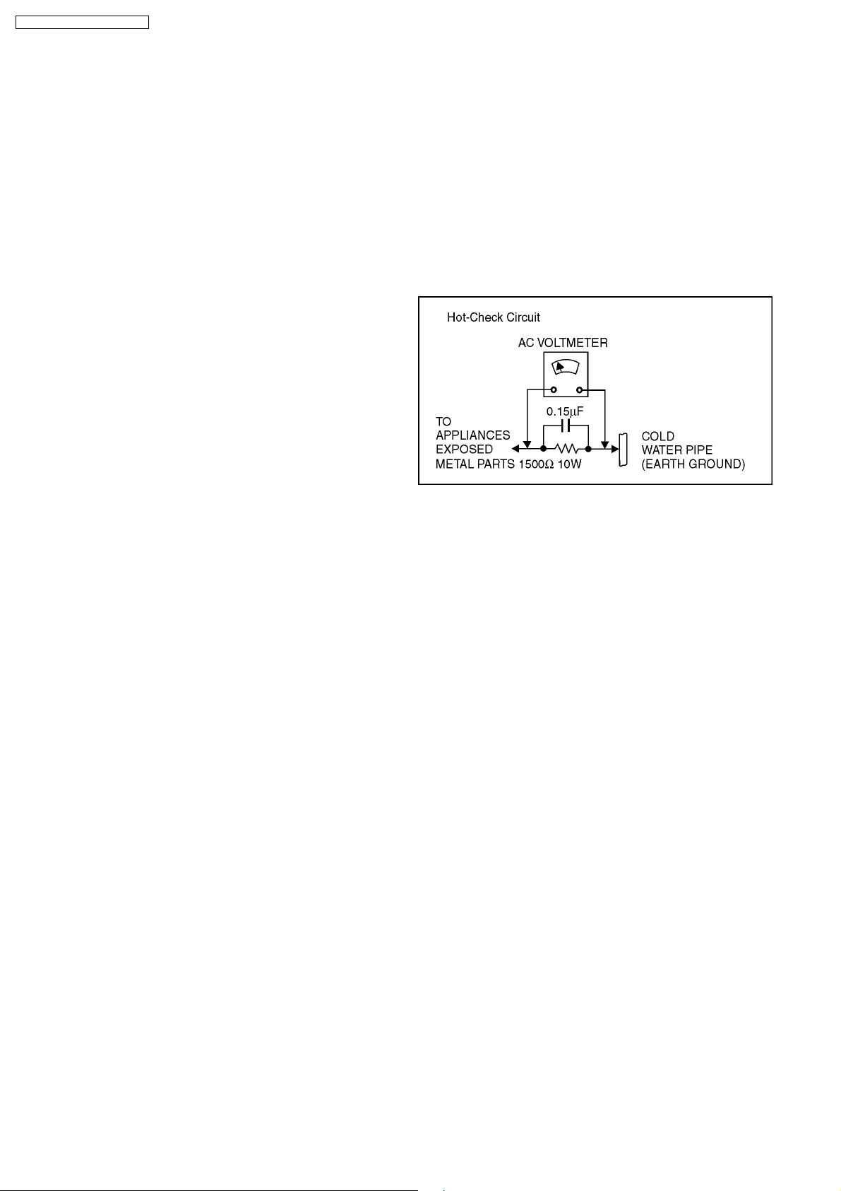
1.1.2. LEAKAGE CURRENT HOT CHECK
1. Plug the AC cord directly into the AC outlet. Do not use an
isolation transformer for this check.
2. Connect a 1.5kΩ, 10 watts resistor, in parallel with a 0.15µF
capacitors, between each exposed metallic part on the set
and a good earth ground such as a water pipe, as shown in
Figure 1.
3. Use an AC voltmeter, with 1000 ohms/volt or more
sensitivity, to measure the potential across the resistor.
4. Check each exposed metallic part, and measure the
voltage at each point.
5. Reverse the AC plug in theAC outlet and repeat each ofthe
above measurements.
6. The potential at any point should not exceed 0.75 volts
RMS. A leakage current tester (Simpson Model 229 or
equivalent) may be used to make the hot checks, leakage
current must not exceed 1/2 milliampere. In case a
measurement is outside of the limits specified, there is a
possibility of a shock hazard, and the equipment should be
repaired and rechecked before it is returned to the
customer.
4
Page 5

2 WARNING
2.1. PREVENTION OF ELECTROSTATIC DISCHARGE (ESD) TO
ELECTROSTATIC SENSITIVE (ES) DEVICES
DMR-EX95VEG / DMR-EX95VEB
Some semiconductor (solid state) devices can be damaged
easily by static electricity. Such components commonly are
called Electrostatic Sensitive (ES) Devices. Examples of typical
ES devices are integrated circuits and some field-effect
transistor-sand semiconductor "chip" components. The
following techniques should be used to help reduce the
incidence of component damage caused by electrostatic
discharge (ESD).
1. Immediately before handling any semiconductor
component or semiconductor-equipped assembly, drain off
any ESD on your body by touching a known earth ground.
Alternatively, obtain and wear a commercially available
discharging ESD wrist strap, which should be removed for
potential shock reasons prior to applying power to the unit
under test.
2. After removing an electrical assembly equipped with ES
devices, place the assembly on a conductive surface such
as aluminum foil, to prevent electrostatic charge buildup or
exposure of the assembly.
3. Use only a grounded-tip soldering iron to solder
or unsolder ES devices.
4. Use only an anti-static solder removal device.
Some solder removal devices not classified
as "anti-static (ESD protected)" can generate electrical
charge sufficient to damage ES devices.
5. Do not use freon-propelled chemicals. These can generate
electrical charges sufficient to damage ES devices.
6. Do not remove a replacement ES device from its protective
package until immediately before you are ready to install it.
(Most replacement ES devices are packaged with leads
electrically shorted together by conductive foam, aluminum
foil or comparable conductive material).
7. Immediately before removing the protective material from
the leads of a replacement ES device, touch the protective
material to the chassis or circuit assembly into which the
device will be installed.
Caution
Be sure no power is applied to the chassis or circuit, and
observe all other safety precautions.
8. Minimize bodily motions when handling unpacked
replacement ES devices. (Otherwise harmless motion such
as the brushing together of your clothes fabric or the lifting
of your foot from a carpeted floor can generate static
electricity sufficient to damage an ES device).
5
Page 6
DMR-EX95VEG / DMR-EX95VEB
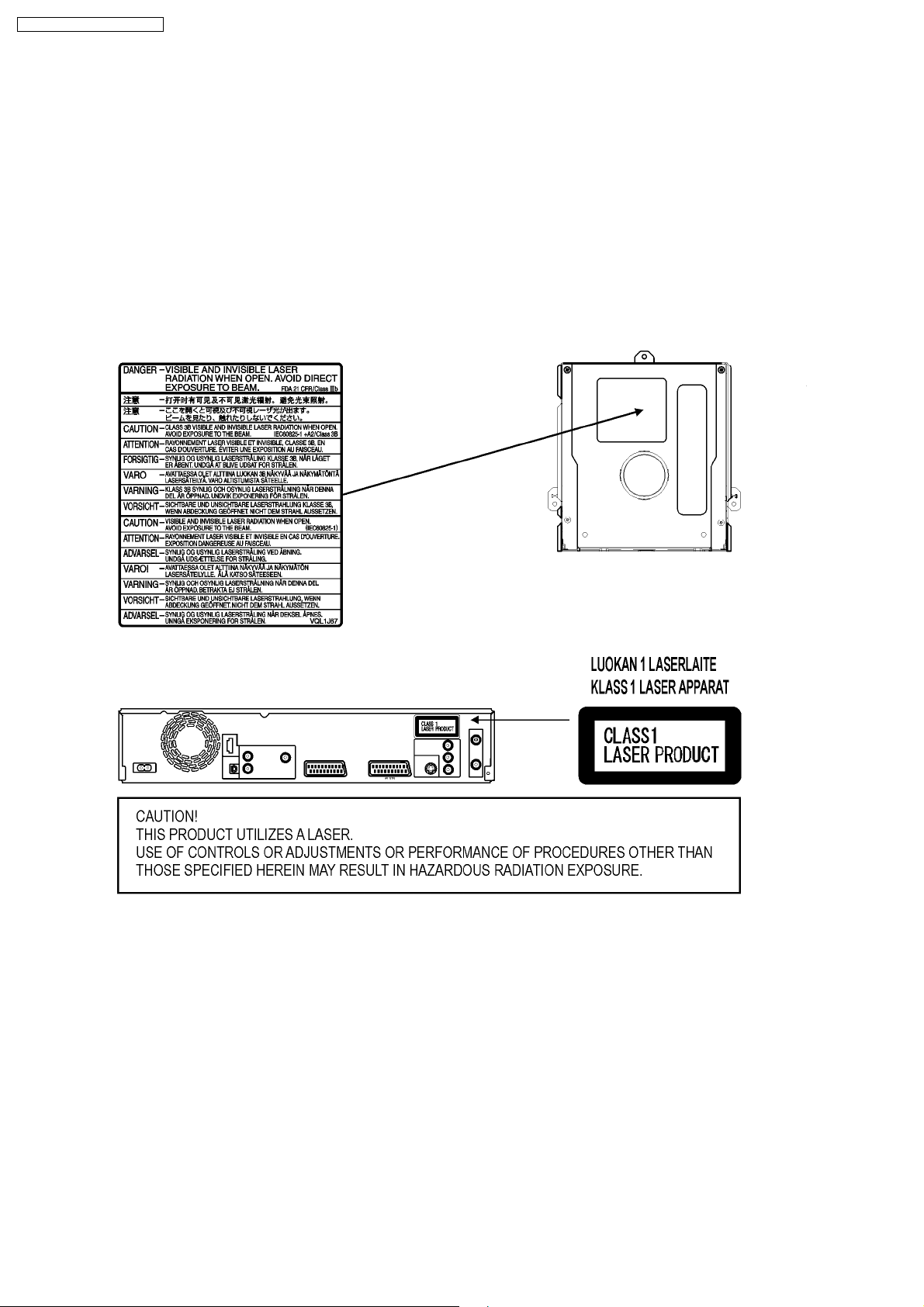
2.2. PRECAUTION OF LASER DIODE
CAUTION: ACHTUNG:
This product utilizes a laser diode with the unit turned “on”,
invisible laser radiation is emitted from the pickup lens.
Wave length: 662 nm/780 nm
Maximum output radiation power from pickup: 100µ W/VDE.
Laser radiation from the pickup lens is safety level, but be sure
the followings:
1. Do not disassemble the optical pickup unit, since radiation
from exposed laser diode is dangerous.
2. Do not adjust the variable resistor on the pickup unit.
It was already adjusted.
3. Do not look at the focus lens using optical instruments. 3. Nicht in die Fokussierlinse blicken.
4. Recommend not to look at pickup lens for a long time. 4. Auch nicht mit optischen Instrumenten in die Fokussierlinse blicken.
Dieses Produkt enthält eine Laserdiode.
Im eingeschalteten Zustand wird unsichtbare Laserstrahlung von der
Lasereinheit ausgestrahlt.
Wellenlänge: 662 nm/780 nm
Maximale Strahlungsleistung der Lasereinheit: 100µ W/VDE.
Die Strahlung der eingeschalteten Lasereinheit ist ungefährlich, wenn
folgende Punkte beachtet werden:
1. Die Lasereinheit nicht zerlegen, da die Strahlung an der freigelegten
Laserdiode gefährlich ist.
2. Den werksseitig justierten Einstellregler der Lasereinheit nicht
verstellen.
6
Page 7
DMR-EX95VEG / DMR-EX95VEB
2.3. SERVICE CAUTION BASED ON LEGAL RESTRICTIONS
General description about lead free Solder (PbF)
•
• The lead free solder has been used in the mounting process of all electrical components on the printed circuit boards used
• •
for this equipment in considering the globally environmental conservation.
•
• The normal solder is the alloy of tin (Sn) and lead (Pb). On the other hand, the lead free solder is the alloy mainly consists
• •
of tin (Sn), silver (Ag) and Copper (Cu), and the melting point of the lead free solder is higher approx. 30 degrees C (86°F)
more than that of the normal solder.
Service caution for repair work using Lead Free Solder (PbF)
•
• The lead free solder has to be used when repairing the equipment for which the lead free solder is used.
• •
•
• To put lead free solder, it should be well molten and mixed with the original lead free solder.
• •
•
• Remove the remaining lead free solder on the PCB cleanly for soldering of the new IC.
• •
•
• Since the melting point of the lead free solder is higher than that of the normal lead solder, it takes the longer time to melt
• •
the lead free solder.
•
• Use the soldering iron (more than 70W) equipped with the temperature control after setting the temperature
• •
at 350±30 degrees C (662±86°F). When soldering or unsoldering, please completely remove all of the solder
on the pins or solder area and be sure to heat the soldering points with the Pb free solder until it melts enough.
Definition of PCB Lead Free Solder being used
•
• The letter of “Pbf is printed either foil side or component side using the lead free solder.
• •
Recommended Lead Free Solder (Service Parts Route.)
•
• The following 3 types of lead free solder are available through the service parts route.
• •
RFKZ03D01K-----------(0.3mm 100g Reel)
RFKZ06D01K-----------(0.6mm 100g Reel)
RFKZ10D01K-----------(1.0mm 100g Reel)
Note
•
• Ingredient: tin (Sn), 96.5%, silver (Ag) 3.0%, Copper (Cu) 0.5%, Cobalt (Co) / Germanium (Ge) 0.1 to 0.3%
• •
7
Page 8

DMR-EX95VEG / DMR-EX95VEB
3 SERVICE NAVIGATION
3.1. SERVICE INFORMATION
This service manual contains technical information which will allow service personnel to understand and service these models.
Please place orders using the parts list and not the drawing reference numbers.
1. This service manual does not contain the following information, because of the impossibility of servicing at component level.
•
• Schematic Diagram, Block Diagram,
• •
Exploded View, Parts List and P.C.B. layout of
RAM / Digital P.C.B. Module and Back End P.C.B. Unit.
2. The following categories are recycling module part.
Please send them to Central Repair Center.
•
• RAM / Digital P.C.B. Module: RFKNEX95VEG
• •
•
• RAM / Digital P.C.B. Module: RFKNEX95VEB
• •
•
• Back End P.C.B. Unit: REPD0031F (EX95EG)
• •
•
• Back End P.C.B. Unit: REPD0031G (EX95EB)
• •
3. If the circuit is changed or modified, this information will be followed by supplement service manual to be filed with original
service manual.
4. Adjustment procedures, Disassembly Procedures and Assembly Procedures for VCR Mechanism Chassis are separate volume
from this service manual. Please refer to the service manual for R4 Mechanism Chassis for EURO model (MAD0403002C2).
3.2. CAUTION FOR DivX (For EG only)
Please give the information “Warning for Customers who use the DivX Video-on-Demand content.” always to the customer
together with the product, if you have to exchange EEPROM, P.C.B. including EEPROM or the product itself.
Also attach these information to every service part (EEPROM or P.C.B. including EEPROM).
This complete Information is needed for every customer who is using the DivX Video-on-Demand Serivce.
Appendix:
* Parts that memorize user’s information are only on the EEPROM.
* The registration of Registration Code is possible for half a year up to 6 recorders up to 10 recorders a year.
Every replacement of EEPROM or P.C.B. including EEPROM spends one of this.
•
• Registration Code is memorized in the EEPROM (RFKFxxxxxxx)
• •
•
• If the Power & Digital I/F P.C.B. or the EEPROM will be changed a new Registration Code
• •
different from the previous one will be generated.
•
• In this case the customer, who is useing DivX Video-on-Demand sercive, can not longer play any content that
• •
was or is purchased under that old registration code.
•
• Therefore the customer will need to register a new registration code.
• •
8
Page 9

4 SPECIFICATION
DMR-EX95VEG / DMR-EX95VEB
Power supply: AC220-240 V, 50/60 Hz
Power consumption: 38 W ±1,3 W
Dimensions and Mass: 430 (W) x 352 (D) x 84 (H) mm
Operating temperature range: +5 to +40 °C
Operating humility range: 35 to 80 % RH (no condensation)
Pickup Laser power: CLASS1
Pickup Wave length: DVD 662 nm / CD 780 nm
Recording format Heads VHS Video Cassette System
Recording system: MPEG2 (Hybrid VBR)
Signal system: PAL 625/50, NTSC 525/60
DVD Region number: Region No. 2
Internal HDD Capacity: 250 GB
DVD Recording /
Playable discs:
Power save mode 3 W ±0,4 W
excluding (protrusions) / 6.4 kg
No hazardous radiation is emitted
with the safety protection
Standard with FM audio
NTSC (only from extern and DVD)
4 Helical Scan Heads for Video
2 Helical Scan Heads for FM audio
1 Fixed Head for Normal audio
Audio: Dolby Digital 2CH
DVD-RAM (12 cm 4.7 GB)
DVD-RAM (12 cm 9.4 GB)
DVD-RAM (8 cm 2.8 GB)
DVD-R (12 cm 4.7 GB)
DVD-R (8 cm 1.4 GB)
DVD-RW (12 cm 4.7GB)
DVD+R (12 cm 4.7 GB)
DVD+RW (12 cm 4.7 GB)
DVD-R DL (12 cm 8.5 GB)
DVD+R DL (12 cm 8.5 GB)
SD Card Slot: JPEG (Still Picture DCF Standard)
TIFF (uncompressed)
MPEG2 (rec. by Panasonic cam)
Campatible Cards: SD Card, Multimedia Card
miniSD™ Card (with adapter)
Card format: FAT12, FAT16
Card picture pixels: 34x34 to 6144x4096
Video input AV1 / AV2: 21 pin connector (1.0 Vp-p 75 Ω )
Video input AV3 / AV4: pin jack connector (1.0 Vp-p 75 Ω)
S-Video input AV1 / AV2: 21 pin connector
(Y: 1.0 Vp-p, C: 0.3 Vp-p 75 Ω)
S-Video input AV3 / AV4: pin jack connector
(Y: 1.0 Vp-p, C: 0.3 Vp-p 75 Ω)
RGB Video input AV3 (PAL): 21 pin connector (0.7 Vp-p 75 Ω)
DV input: IEEE 1394 Standard 4 pin
Video output AV1 / AV2: 21 pin connector (1.0 Vp-p 75 Ω)
FBAS Video output (composit): pin jack connector (1.0 Vp-p 75 Ω)
S-Video output AV1: 21 pin connector (1.0 Vp-p 75 Ω)
S-Video output (cinch): pin jack connector (1.0 Vp-p 75 Ω)
S-Video output: S connector (1.0 Vp-p 75 Ω)
RGB Video output AV1: 21 pin connector (0.7 Vp-p 75 Ω)
Component Video output: Y pin jack (1.0 Vp-p 75 Ω)
PB pin jack (0.7 Vp-p 75 Ω)
PR pin jack (0.7 Vp-p 75 Ω)
HDMI output (19 pin type A): Version 1.2a (EDID Vers. 1.3)
Audio input AV1 / AV2: 21 pin connector (-6 dBV 500 mV)
Audio input AV3 / AV4: pin jack (-6 dBV 500 mV)
Audio output (cinch): pin jack (-6 dBV 500 mV)
Optical output: PCM, Dolby Digital, DTS, MPEG
Videotape speed and Recording time (PAL/SECAM 240 min. tape):
SP: 23.39 mm/s, 240 min.
LP: 11.695 mm/s, 480 min.
EP: 7.796 mm/s, 720 min.
FF/REW time: 60 sec. (180 min. tape)
Videotape speed and Recording time (NTSC 240 min. tape):
SP: 33.35 mm/s, 168 min.
EP: 11.12 mm/s, 505 min.
DVD approximate Recording
time:
Additional playable discs: DVD-RAM (VR format)
TV tuner system EB (PAL): UHF: CH21-CH68 (analog/DVB-T)
TV tuner system EG (PAL): UHF: CH21-CH69 (analog/DVB-T)
RF Converter Output: not provided
XP: 10 MBps (60 min)
SP: 5 MBps (120 min)
LP: 3 MBps (240 min)
EP: 1.7 / 1.2 MBps (360 - 480 min)
DVD-RW (VR format)
DVD-R (MP3, JPG)
DVD-R DL, DVD+R DL
DVD-Video, DVD-Audio
CD-Audio (CD-DA), Video CD
SVCD (IEC62107)
CD-R, CD-RW
CD-DA, MP3, JPG, VCD,
DivX formatted discs (for EG only)
VHF: CH E2-CH E12 (analog)
VHF: CH 05-CH 12 (DVB-T)
CATV: CH S01-S05(S1-S3)
CATV: S1-S20(M1-U10), S21-S41
Winding Speed
(180 min. tape):
FF time approximate 60 sec.
REW time approximate 43 sec.
Note:
Specifications are subject to change without notice.
Mass and dimensions are approximate.
■ Build-in decoders: You can play discs with following symbols
9
Page 10
DMR-EX95VEG / DMR-EX95VEB
5 NEW FEATURE
5.1. ABOUT DivX (EXCEPT EB)
5.1.1. GENERAL
DivX is a new video compressing format that is applied
MPEG-4 technology to improve quality and the compressibility
and it is developed by the DivXNetworks, Inc., Video file of high
resolution and the high picture quality can be made thought it
is a high compressibility.
DivX codec is necessary for converting video to DivX file and
playback files made.
5.1.2. OPERATING INSTRUCTIONS
ABOUT DivX VIDEO-ON-DEMAND
CONTENT
DivX Video-on-Demand (VOD) content is encrypted for
copyright protection. In order to play DivX VOD content on this
unit, you first need to register the unit.
Follow the online instructions for purchasing DivX VOD content
to enter unit’s registration code and register unit. Visit
www.divx.com/vod for mor information.
Display unit’s registration code:
When playing this content
•
• Number of remaining plays is reduced by one if
• •
−
− you press [POWER]
− −
−
− you press [STOP]
− −
−
− you press [backwards SKIP],
− −
[backwards SLOW / SEARCH] or
[forwards SLOW / SEARCH]
etc. and arrive at another content or start of content
being played.
−
− scheduled [DRIVE SELECT] to change drive
− −
* Resume functions do not work.
Typical Playback procedure of DivX VOD
(Video On Demand):
Case 1 When DivX VOD is used newly.
Case 2 When EEPROM or P.C.B. includin EEPROM was
Case 3 When recorder was exchanged to another recorder for
Case 4 When customer own second recorder.
Case 5 When owner of recorder was changed to another.
replaced for repairing.
repairing.
•
• We recommend that you make a note of this code for future
• •
reference.
•
• After playing DivX VOD content for first time, another
• •
registration code is then displayed in “DivX Registration”. do
not use this registration code to purchase DivX VOD
content. If you use this code to purchase DivX VOD content
and the play content on this unit, you will no longer be able
to play any content that you purchased using previous
code.
•
• If you purchase DivX VOD content using a registration code
• •
different from this unit’s code, you will not be able to play
this content. (“Authorization Error” is displayed.)
Some DivX VOD content can only be played a set number of
times.
When you play this content, remaining number of plays is
displayed. You cannot play this content when number of
remaining plays is zero. (“Rental Expired” is displayed.)
10
Page 11
DMR-EX95VEG / DMR-EX95VEB
CASE 1 WHEN DivX IS USED NEWLY
Registration Code display (code is an example)
Case 1
Activation: File obtaining (code/ID are examples)
Ovtainment/Playback of additional file after Activation
(code/ID is an example)
CASE 2 WHEN EEPROM OR P.C.B. INCLUDING EEPROM
WAS REPLACED FOR REPAIRING
CASE 3 WHEN RECORDER WAS EXCHANGED TO ANOTHER
RECORDER FOR REPAIRING
New Registration Code is displayed (code is an example)
Activation: File Playback
Registration Code display (code is an example)
Case 2
Activation: File obtaining (code/ID are example)
11
Page 12
DMR-EX95VEG / DMR-EX95VEB
Activation: File Playback
Registration Code display after Activation (example)
Activation: File obtaining (code/ID are example)
Activation: File Playback
Obtainment/Playback od additional file after Activation
(code/ID is an example)
Case 3
CASE 4 WHEN CUSTOMER OWN SECOND RECORDER
Registration Code display of second recorder (code is an example)
Registration Code display after Activation (example)
Case 4
12
Page 13
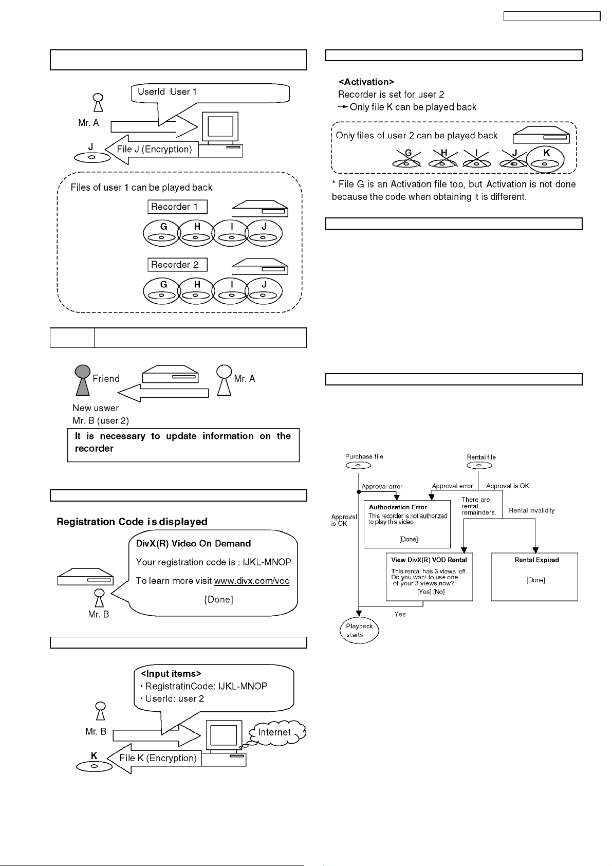
DMR-EX95VEG / DMR-EX95VEB
Obtainment/Playback od additional file after Activation
(code/ID is an example)
CASE 5 WHEN OWNER OF RECORDER WAS CHANGED TO
ANOTHER
Activation: File Playback
FILE KIND
(There are two kinf of Activation files as follows too.)
•
• Rental: There is a playback limitation
• •
•
• Purchase: Unrestricted
• •
Also there is next file as DRM files besides the abovementioned.
•
• Base:
• •
It is not necessary to approve though the contents is being
endode.
If it is recorder/player for DRM, any can play back. (It is the
same as usual DivX file when seeing from user.)
SCREEN SHIFT (Error display)
Case 5
Activation
Activation: File obtaining (code/ID are example)
Wheter approval is OK or not.
Wheter the recorder is corresponding to User information on
the file or not.
13
Page 14

DMR-EX95VEG / DMR-EX95VEB
5.1.3. ABOUT DivX DRM
Divx file includes file to which DRM(Digital Right Management) is applied and file not applied. This item is a content that relates only
in treating file to which DRM is applied.
1. Registration Code display function
2. User’s registration and approval function
3. Rental management function
5.1.3.1. REGISTRATION CODE DISPLAY FUNCTION
Registration Code is alphanumeric character sequence 8 bytes inputted as recorder information, in case a use purchases or rent
a DivX DRM file in a network. Registration code is a character sequence generated at random, and differs in each recorder.
Moreover, Registration code is updated by new user authentication ever if same recorder.
5.1.3.2. USER’S REGISTRATION AND APPROVAL FUNCTION
•
• Only one user can register for one recorder. If user’s
• •
registration is not done with the recorder, DivX file cannot
be played back.
•
• User’s registration is performed only when a DivX DRM
• •
file is first chosen by recorder
•
• DivX DRM file that can perform user’s registration is only a file that is registered Registration Code and purchased or rented.
• •
•
• User authentication is performed whenever DivX DRM file is played back. Error message is displayed when failing in user’s
• •
registration and approval.
5.1.3.3. RENTAL MANAGEMENT FUNCTION
There are purchase file without registration of number of playback and rental files with registration of number of playback as Divx
file. Number of playback of rental file is counted by the recorder. When rental file is played, remaining number of times that can be
played back will be shown to users, recorder requests users to input yes or no. Following specifications have been installed for the
rental files in the purpose to clarify the count condition of number of times of playback.
•
• Conditions on counting number of times of play.
• •
1. When a file was opened successfully. (At the time of playback start)
2. When you have done review operation from the start. (Skip to file head)
−
− At this time, remaining number of times that can be played back and confirmation message
− −
[Do you play really?] are displayed.
−
− When the playback point has been skipped to the top of title, number of playback is not counted if the top of title was
− −
not recognized.
−
− Even if the power failure occurs after start of playback of rental file, number of times of playback counted at start of the
− −
playback is held as it is.
(Though playback stops by power failure,
the number of times of playback is not counted.)
When it has reached head of title, the playback is ended, and screen becomes DivX menu (There is no resume) and then cursor
is located on title that has been played back.Then if the same file was continuously played back, it begins to playback from the
file head.
Note:
Above mentioned stored user information and number of times of playback are not erased by update of firmware or by
initialization by test mode.
14
Page 15

DMR-EX95VEG / DMR-EX95VEB
5.2. HDAVI CONTROL (HDMI LINK)
Linked operations by HDAVI Control (HDMI Link)
5.2.1. WHAT IS HDMI
HDMI is abbreviation of [High-Definition Multimedia Interface], and is digital interface standard for next generation TV
corresponding to follows.
1. Non-compressing high quality digital image
2. Digital transmission of multi channel digital audio.
3. Two way communication of control signal of control straightening between equipments.
Cable Transmission
HDMI
Cable
method
Digital
(~4.455Gbps)
Directionality Transmission
signal
One-way Digital image
(none-compression highdefinition television image)
One-way Digital Audio
(6ch/24 bit high sound quality
PCM of DVD audio/Bit stream
of surround to 8ch of DVD
video)
Interactive Digital control signal
(Advanced control between
equipments)
Feature
Clock line in one system and data line in three systems
can high-speed communicate high reliability because of
balance communication that uses three respectively
every one system.
Moreover, because high-speed data line in three system
can be used at same time, it has ten of other digital
cables times or more transmission ability.
And can transmit high-definition television image of noncompression, 24 bit high sound quality PCM voice of
multi-CH of DVD audio (to 6ch) and Bit stream signal of
surround to 8ch of DVD video (5.1ch, 6.1ch, and 7.1ch,
etc.) as a digital signal of no deterioration.
It has power supply line and a interactive control signal
line communication independent of AV signal, a Cd can
an advanced control between equipments. Therefore it
can correspond to making of AV equipment in the future
highly a network.
5.2.2. LINK FUNCTIONS
Functions
(1) Automatic Input switch
(2) Link of Power
15
Page 16
DMR-EX95VEG / DMR-EX95VEB
5.2.3. OUTLINE OF EQUIPMENTS
LINKED FUNCTIONS
1. Automatic Input switch
At starting of playback / GUI (Graphical User Interface)
display by DIGA, it turn on power of VIErA, and it displays
picture of DIGA onto screen of VIErA.
a. Starting of playback:
It includes automatic playback of DVD-Video and so on.
And it includes picture of screen saver too.
b. GUI display:
FUNCTIONS, DIRECT NAVIGATOR, TV PROGRAM,
PROG/CHECK, Timer Recording, G-code, Initial setting,
Playback setting, Play list, SD/DVD guide, Warning
messages that user can select and so on.
2. Power Link
Power of DIGA is turned off linking to POWER OFF of
VIErA.
•
• Power not turned on linking to POWER ON of VIErA.
• •
•
• It is limited in following cases that DIGA links to POWER
• •
OFF of VIErA.
•
• During EE display (While Timer recording is being
• •
executed/Functions is being displayed are included.)
However except cases below.
•
• During EE display, but manual recording is being
• •
executing/during EXT_Link recording.
•
• During Tray is being opened.
• •
•
• Case that DIGA is in status that power cannot turn off
• •
(during dubbing, during finalize).
16
Page 17
6 LOCATION OF CONTROLS AND COMPONENTS
Remote Control
DVD/VHS
Stand-by/on switch
Press to switch the unit from on to stand-by mode
or vice versa. In stand-by mode, the unit is still consuming
a small amount of power.
Switching this unit into standby mode does not
disconnect it from the mains.
DRIVE
SELECT
Select the HDD, DVD or SD drive.
Direction buttons in the menu guide.
Select groups or titles.
ENTER
OK
ENTER: Select or save a setting.
Still picture or slow motion playback.
Display the programme information from
the TV GUIDE or the Banner.
PROG/CHECK
Check / Change a Timer recording.
SUB MENU
Launch DVD sub menus.
S
RETURN
Return to the previous menu.
VIDEO Plus+
VIDEO Plus+ menu (EB-model)
ShowView
ShowView menu (EG-model)
SLOW/SEARCH
Search or slow motion playback.
REW: VHS Jet Rewind and Rewind Search
REW
FF
FF: VHS Forward Search
TV
AV
CH
TRACKING/V-LOCK/PAGE
+
CH
-
2
5
4
0
RESET
INPUT
SELECT
DELETE
Turn the television set on and off.
Select the AV input on the television set.
CH: Select the channel on the television set.
VOLUME
VOLUME: Volume control of the television set.
CH: Select the channel on the Recorder.
PAGE: Scroll in the electronic TV Guide.
TRACKING / V-LOCK: Optimise the VHS
playback picture.
Number buttons - direct input
3
6
VCD
9
JPEG
JPEG
MP3
0
5
5:
0
0
5:
5:
5
0
0
0
15:
15:
5
15:
GUIDE: Launch the TV Guide menu.
DIRECT NAVIGATOR: title view
TOP MENU: Main menu of DVD-video.
FUNCTION selection menu.
Cancel a function.
Reset the VHS tape counter.
Switch button of the AV input between AV1, AV2
AV3 (front), AV4 and DV in.
Delete a title.
DVD/VHS
DRIVE
SELECT
5
1
0
5
1
5
0
1
0
SUB MENU
S
DMR-EX95VEG / DMR-EX95VEB
TV
VOLUME
CH
AV
TRACKING/V-LOCK/PAGE
5
0
PAUSE
ENTER
OK
CHAPTER
REC MODE
EXT LINK
STTL
3
+
6
-
VIDEO Plus+
DELETE
INPUT
SELECT
SLOW/SEARCH
REW
PLAY
PROG/CHECK
RETURN
CREATE
MANUAL SKIP
DIRECT TV REC
DISPLAY
TIME SLIP
JET REW
CH
FF
112
4
77889
RESET
SKIP/INDEX
STOP
REC
TEXT
Stops recording, replay or forward / reverse action
STOP
Hold more than 3 seconds to eject the VHS tape.
Pause a recording or playback.
PAU SE
Hold more than 2 seconds for VHS slow-motion playback.
REC
Start the recording.
REC MODE
Record mode button XP, SP, LP, EP
EXT LINK
Record with external recording control.
DIRECT TV REC
Direct TV recording.
TEXT
Launch the MHEG Service (EB-model).
AUDIO
Select the audio channel/soundtrack (EG-model).
STTL
Displays subtitles (EB-model)
F Rec
Flexible Recording (EG-model)
DISPLAY
Launch the disc menus.
PLAY
Starts playback.
RAM - You can increase the playback speed
.
Hold PLAY during playback.
VHS - Playback or continuous playback
SKIP: Skip chapters, titles, or pictures.
SKIP/INDEX
INDEX: Find the beginning of a VHS recording.
Menu guide (red button): Profile, GUIDE, MHEG, Manual Tuning
Menu guide (green button): Profile, GUIDE, MHEG
CREATE
Menu guide (yellow button): Profile, GUIDE, MHEG
CHAPTER
CREATE CHAPTER: Deviding a recording into chapters.
MANUAL SKIP
Menu guide (blue button): Profile, GUIDE
MANUAL SKIP: Jump forwards 30 seconds.
TIME SLIP
Select the time frame.
Jet rewind to the beginning of the VHS tape.
JET REW
17
Page 18
DMR-EX95VEG / DMR-EX95VEB
7 OPERATING INTRUCTIONS
7.1. (DVD) TAKING OUT THE DISC FROM RAM-DRIVE UNIT WHEN THE
DISC CANNOT BE EJECTED BY OPEN/CLOSE BUTTON
7.1.1. (DVD) FORCIBLE DISC EJECT
7.1.1.1. (DVD) WHEN THE POWER CAN
BE TURNED OFF.
1. Turn off the power and press [STOP], [CH UP] keys on the
front panel simultaneously for 5 seconds.
7.1.1.2. (DVD) THE POWER CAN NOT BE
TURNED OFF.
1. Press [POWER] key on the front panel for over 10 seconds
to turn off the power forcibly and press [STOP] [CH UP]
keys on the front panel simultaneously for 5 seconds.
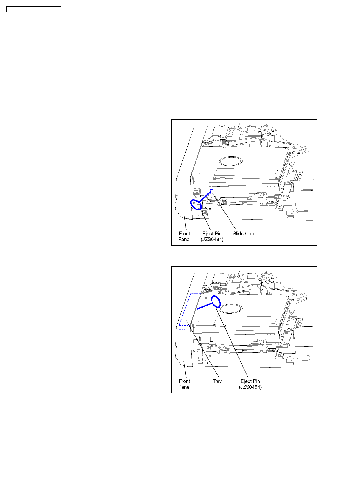
7.1.2. (DVD) WHEN THE FORCIBLE DISC
EJECT CAN NOT BE DONE.
1. Turn off the power and pull out AC cord.
2. Remove the Top Case.
3. Push in SLIDE CAM by Eject Pin (JZS0484) or minus screw
driver (small) to eject tray slightly.
4. Push out Tray by Eject Pin (JZS0484) or minus screw driver
(small).
18
Page 19
7.2. (VHS) REMOVING OF
CASSETTE TAPE
When the cassette tape could not be removed after an
electrical malfunction, there are 2 ways to remove a cassette
tape.
7.2.1. (VHS) REMOVAL BY
COMPULSORY UNLOADING.
If Service Mode can be activated when the power can not be
turned on, this operation is able.
1. Press [STOP] and [EJECT] button simultaneously for more
than 3 seconds and set Drive to [VHS] and set the Service
Mode to 7.
2. Press [STOP] button in order to unload the mechanism.
(Pay attention to tape slack)
Service Mode Display:
7 ** ** (STOP) → 7 0L ** (EJECT)
7.2.2. (VHS) REMOVAL BY MANUAL
OPERATION.
DMR-EX95VEG / DMR-EX95VEB
3. Stop unloading just before unloading willbe completed. The
tape becomes slack.
4. Rotate the S-Reel by a small minus screwdriver to remove
the slack tape.
1. Disconnect the AC plug, and remove the Top Panel and the
Front Panel by referring to the Disassembly Procedures.
2. Connect a batterie (9V spec.) to the Loading Motor in series
for supplying 9V to rotate the Loading Motor.
5. Then unload again to remove the cassette tape.
19
Page 20
DMR-EX95VEG / DMR-EX95VEB
7.2.3. (VHS) TAKE OUT CASSETTE TAPE
MANUALLY AFTER REMOVING
THE MECHANNISM
1. Disconnect the AC plug, and remove the Top Panel, Front
Panel and the Mechanism by referring assembling and
disassembling description.
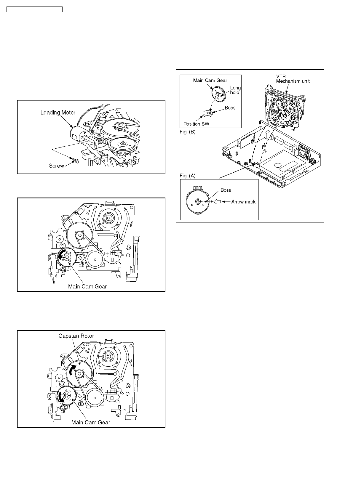
2. Remove the Screw and remove the Loading Motor.
6. Attach Loading Motor and tighten the screw.
7. Set the Position Switch to EJECT POSITION certainly and
attach the mechanism to chassis.
3. Rotate the Main Cam Gear counter-clockwise until just
before the unloading will be completed.
4. Rotate the Capstan Motor clockwise to remove the slack
tape.
5. Rotate the Main Cam Gear counter-clockwise again to
remove the cassette-tape.
20
Page 21

DMR-EX95VEG / DMR-EX95VEB
8 SERVICE MODE
8.1. (DVD) SELF-DIAGNOSIS AND SPECIAL MODE SETTING
8.1.1. (DVD) SELF-DIAGNOSIS FUNCTIONS
Self-Diagnosis Function provides information for errors to service personnel by “Self-Diagnosis Display” when any error has
occurred.
U**, H** and F** are stored in memory and held.
You can check latest error code by transmitting [0] [1] of Remote Controller in Service Mode.
Automatic Display on FL will be cancelled when the power is turned off or AC input is turned off during self-diagnosis display is ON.
Error Code Diagnosis contents Description Monitor Display Automatic FL display
IR ERR IR communication error [IR ERR] is display when communication
between Timer microprocessor and IR
microprocessor fails.
No display
No REC Recording is impossible [No REC] is displayed when recording is
U30 Remote control code error Display appears when main unit and remote
U50 Antenna Short Short circuit was detected at antenna input.
U59 Abnormal inner temperature
detected
U61 The unit is carrying out its
recovery process (with no
disc in the disc tray).
U71 HDMI incompatible
error(HDCP incompatible)
U72 HDMI connection error
(communication error)
U73 HDMI connection error
(authentication error)
impossible due to the defect, dirt or wound
of media.
controller codes are not matched.
Please check antenna.
Display appears when the drive temperature
exceeds 70°C.
The power is turned off forcibly.
For 30 minutes after this, all key entries are
disabled. (Fan motor operates at the highest
speed for the first 5 minutes. For the
remaining 25 minutes, fan motor is also
stopped.) The event is saved in memory as
well.
* The unit detected an error while recording
or playing with with no disc in the disc
tray.
The unit is carrying out its recovery process.
This process restores the unit to normal
operation. The unit is not broken. Wait until
the message disappears.
Display this error when the equipment
(compatible with DVI such as TV, amplifier
etc.) connected to the unit by HDMI is
incompatible with HDCP. *HDCP=Highbandwidth Digital Content
Protection.
This error is displayed when there are any
communication problems with the unit and
the equipments (TV, amplifier etc.)
connected to the unit by HDMI. (or when
there is a problem with the HDMI cable).
When authentication error occurs while the
equipments (TV, amplifier etc.) are
connected by HDMI. (or when there is a
problem with the HDMI cable).
No display
No display
’Short Circuit was
detected at the
antenna input.
Please check your
antenna...’
No display
No display
No display
No display
No display
“*” is remote controller code of the
main unit.
Display for 5 seconds.
Display for 5 seconds.
“U59 is displayed for 30 minutes.
“U72” display disappears when
error has been solved by
Power OFF/ON of connecting
equipment or by inserting/removing
of HDMI cable.
“U73” display disappears when
error has been solved by Power
OFF/ON of connecting equipment
or by inserting/removing of HDMI
cable.
21
Page 22
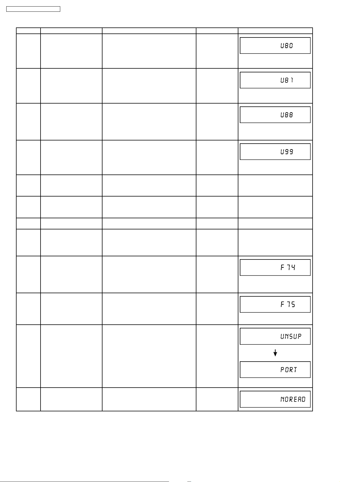
DMR-EX95VEG / DMR-EX95VEB
Error Code Diagnosis contents Description Monitor Display Automatic FL display
U80 ST Microprocessor
Communication Error on
Displayed appears when ST Microprocessor
Communication Error on Timer Bus occurs.
No display
Timer Bus
“U80” is displayed till Power Key is
pressed.
U81 ST Microprocessor
Communication Error on
Displayed appears when ST Microprocessor
Communication Error on UART occurs.
No display
UART
“U81” is displayed till Power Key is
pressed.
U88 The unit is carrying out its
recovery process (with no
disc in the disc tray).
* The unit detected an error while recording
or playing with with no disc in the disc
tray.
No display
The unit is carrying out its recovery process.
This process restores the unit to normal
operation. The unit is not broken. Wait until
the message disappears.
U99 Hang-up Displayed when communication error has
No display
occurred between Main microprocessor and
Timer microprocessor.
Displayed is left until the [POWER]
key is pressed.
H19 Inoperative fan motor When inoperative fan motor is detected after
No display No display
powered on, the power is turned off
automatically.
The event is saved in memory.
F00 No error information Initial setting for error code in memory
No display No display
(Error code Initialization is possible with error
code initialization and main unit
initialization.)
F58 Drive hardware error When drive unit error is detected, the event
No display No display
is saved in memory.
F34 Initialization error when main
microprocessor is started up
for program recording
When initialization error is detected after
starting up main microprocessor for program
recording, the power is turned off
No display No display
automatically.
The event is saved in memory.
F74 HDIM Device Key
Communication error.
HDMI connection could not be authenticated
due to a transfer malfunction.Factor of HDMI
No display
Device key-road failure- When HDMI LSI is
damaged.- When the bus line of I2C doesn´t
operate normally.- When device key
information
recorded is damaged.
F75 HDIM Device Key Information
error.
HDMI connection could not be authenticated
due to an internal data malfunction.Factor of
No display
HDMI Device key-road failure- When HDMI
LSI is damaged.- When the bus line of I2C
doesn´t operate normally.- When device key
information recorded is damaged.
UNSUPPORT
Unsupported disc error *An unsupported format disc was played,
although the drive starts normally.
“This disc is
incompatible.”
*The data format is not supported, although
the media type is supported.
*Exceptionally in case of the disc is dirty.
NO READ Disc read error *A disc is flawed or dirty.
*A poor quality failed to start.
*The track information could not be read.
Display for 5 seconds.
“Cannot read.
Please check the
disc.”
22
Page 23
DMR-EX95VEG / DMR-EX95VEB
Error Code Diagnosis contents Description Monitor Display Automatic FL display
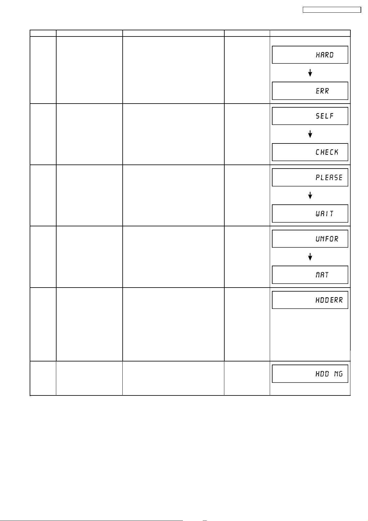
HARD
Drive error The drive detected a hard error. “DVD drive error.” Display for 5 seconds.
ERR
SELF
CHECK
PLEASE
WAIT
UNFORMAT
Restoration operation Since the power cord fell out during a power
failure or operation, it is under restoration
operation.
*It will OK, if a display disappears
automatically. If a display does not
disappear, there is the possibility that
defective Digital P.C.B. / RAM drive.
Unit is in termination process Unit is in termination process now.
“BYE” is displayed and power will be turned
off.
In case “Quick Start” of setup menu is ON, it
is displayed in restoration operation for AC
off.
Unformatted disc error You have inserted an unformatted DVD-
RAM or DVD-RW that is unformatted or
recorded on other equipment.
No display
No display
Format:
This disc is not
formatted properly.
Format the disc in
DISK
MANAGEMENT?
HDD ERR [HDD ERR] is displayed
when start up of HDD was
failed.
(Except error of setting of
Power on Stand-by)
HDD NG Power on Stand-by setting
error
1. When normal start up was failed
2. When start up at HDD boot was failed
3. When start up from state of P-OFF was
failed
4. When start up from state of HDD
SLEEP was failed.
[HDDERR] is displayed when above each
start up of HDD was failed.
* In case 1.), tray opens automatically and
[HDDERR] is displayed until version up disc
is inserted.
[HDD NG] is displayed when power on
Stand-by setting of HDD is NG or when
HDD which power on Stand-by is not set to
is used.
Please try to replace HDD with junine HDD
as service parts.
No display
No display
23
Page 24
DMR-EX95VEG / DMR-EX95VEB
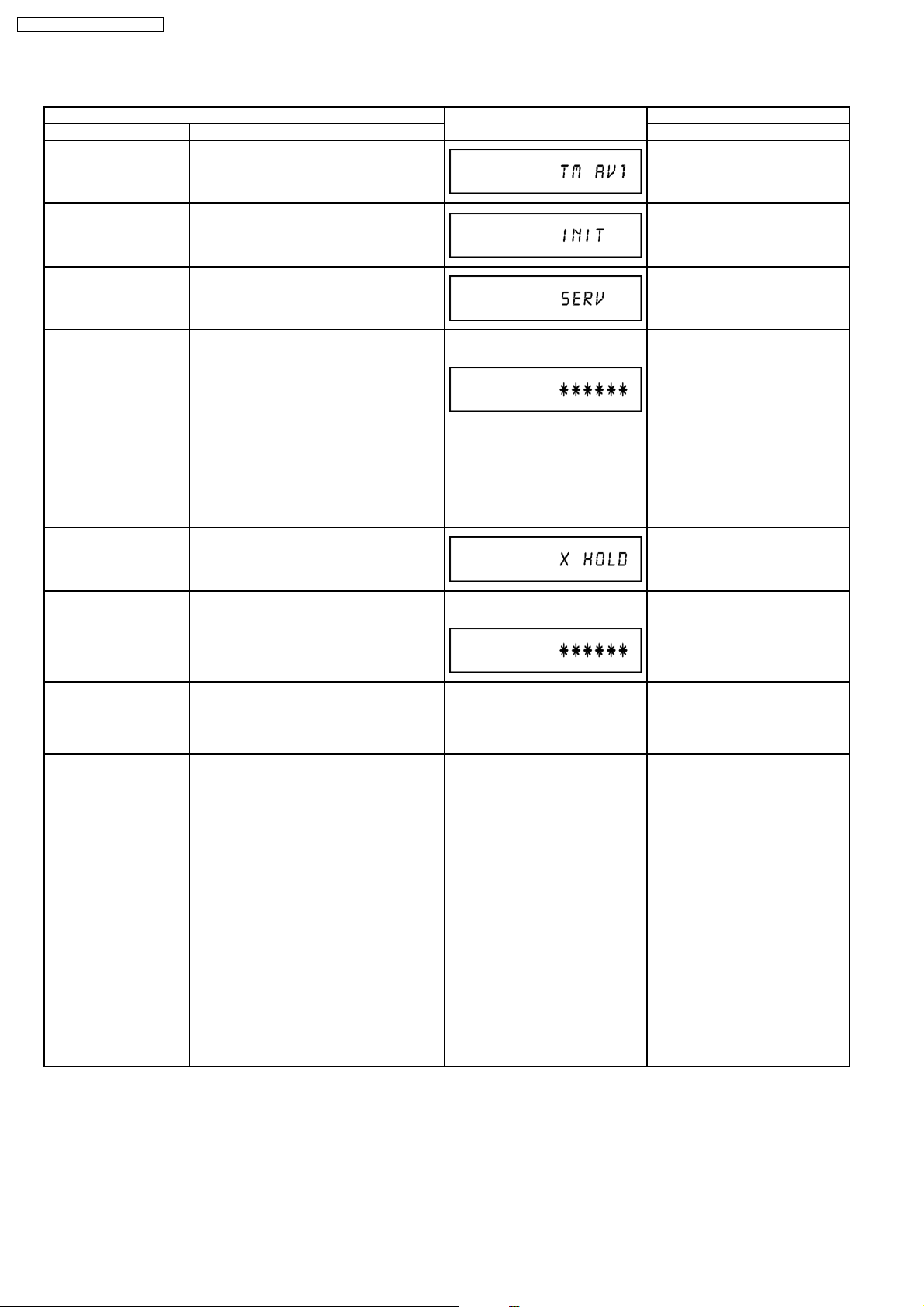
8.1.2. SPECIAL MODES SETTING
Item FL display Key operation
Mode name Description Front Key
TEST Mode *All the main unit´s parameters (include
tuner) are initialized.
Rating password The audiovisual level setting password is
initialized to “Level 8”.
Press [VHS to DVD COPYING],
[REC] and [OPEN/CLOSE] keys
simultaneously for five seconds
when power is off.
Open the tray, and press [REC]
and [PLAY] simultaneously for 5
seconds.
Service Mode Setting every kind of modes for servicing.
Forced disc eject Removing a disc that cannot be ejected.
Child lock/unlock Set or release “Child Lock”. Press [ENTER] and [RETURN] by
NTSC/PAL system select To switch PAL/NTSC altemately. The display before execution
Forced power-off When the power button is not effective while
Aging Perform sequence of modes as * Aging
*Details are described in “Service Mode”.
The tray will open and unit will shift to P-off
mode.
*When Timer REC is ON or EXT-LINK is
ON, execute " Forced disc eject " after
releasing Timer REC or EXT-LINK.
*This command is not effective during "Child
lock" is ON.
While Demonstration Lock is being set, this
Forced disc eject function is not accepted.
If this command was executed while
TIMER REC is being set, TIMER REC
setting will turn to OFF.
power is ON, turn off the power forcibly.
*When Timer REC is ON or EXT-LINK is
ON, execute “Forced Power-off” after
releasing Timer REC or EXT-LINK.
Description shown below continually.
Caution:
All programs in DVD-RAM disc will be
deleted because Formatting is done once
in Aging process.
The display before execution
leaves.
leaves.
Display in P-off mode. Press [Power] key over than 10
Display following the then mode. When the power is ON, press [CH
When the power is off, press
[STOP], [OPEN/CLOSE] and [VHS
to DVD COPYING] keys
simultaneously for 5 seconds.
When the power is off, press
[STOP] and [CH UP] keys
simultaneously for 5 seconds.
remote controller simultaneously
until [X-HOLD] is displayed.
While the power is on (E-E mode),
press [STOP] and [OPEN/CLOSE]
simultaneously for 5 seconds.
seconds.
DOWN], [VHS to DVD COPYING]
and [OPEN/CLOSE]
simultaneously for over 5 seconds
and less than 10 seconds.
NOTE1:
If Unit has not turned into Aging
mode by operations shown above,
execute TEST MODE once and reexecute operation shown above.
(*All the main unit’s parameters
include tuner are initialized by
TEST mode.)
24
NOTE2:
If the unit has hung-up because of
pressing keys for over 10 seconds,
once turn off the power, and reexecute this command.
*When releasing Aging mode,
press [POWER] key.
Page 25
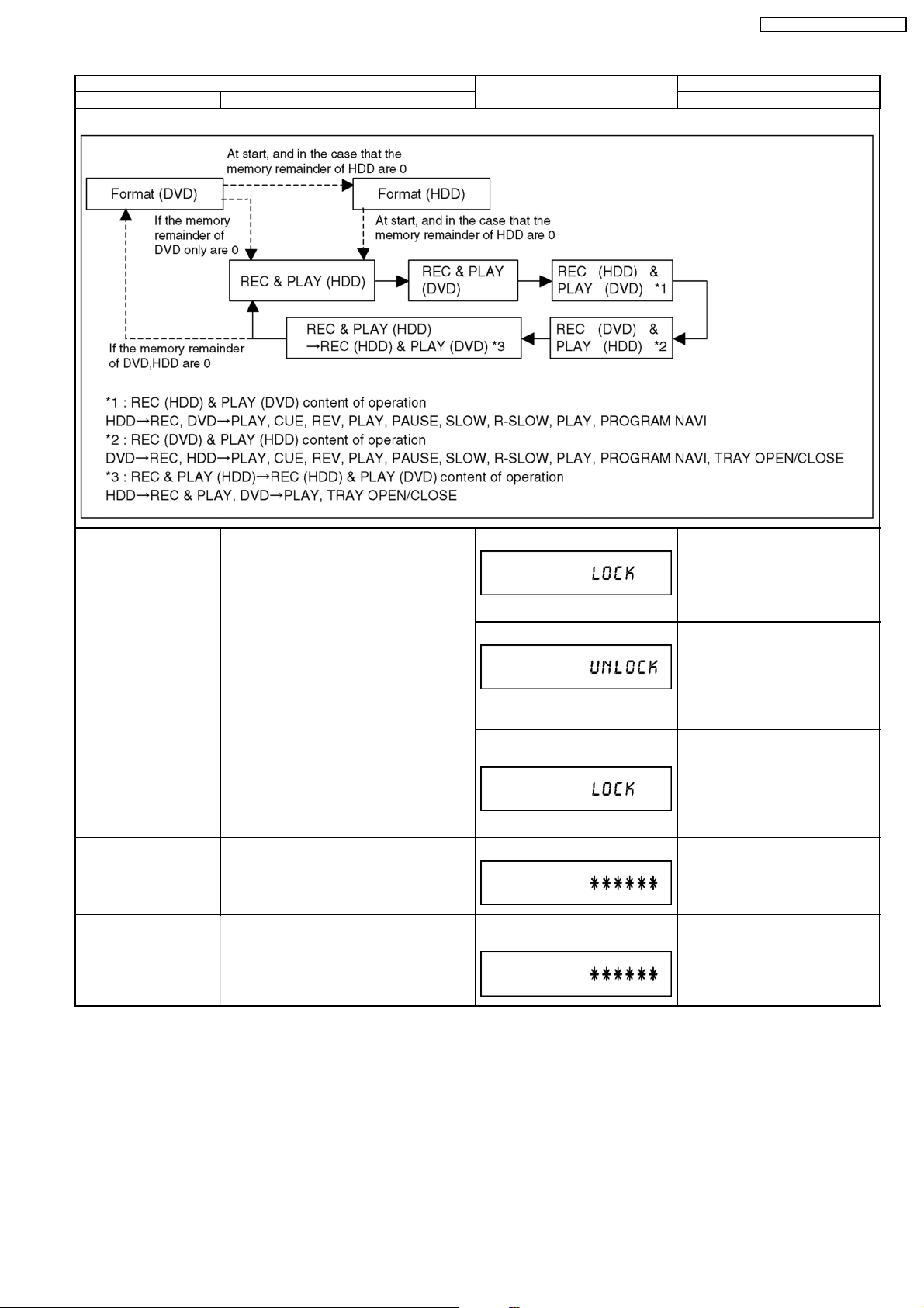
DMR-EX95VEG / DMR-EX95VEB
Item FL display Key operation
Mode name Description Front Key
Aging Contents (Example):
Demonstration
lock/unlock
Ejection of the disc is prohibited.
The lock setting is effective until unlocking
the tray and not released by “Main unit
*When lock the tray.
When the power is on, press
[STOP] and [POWER] keys
simultaneously for 5 seconds.
initialization” of service mode.
“LOCK” is displayed for 3 seconds.
*When unlock the tray.
When the power is on, press
[STOP] and [POWER] keys
simultaneously for 5 seconds.
“UNLOCK” is displayed for 3
seconds.
*When press OPEN/CLOSE key
while the tray being locked.
Press [OPEN/CLOSE] key while
the tray being locked.
Display “LOCK” for 3 seconds.
ATP re-execution Re-execute ATP. Display at ATP executing. When the power is on (E-E mode),
press [CH UP] and [CH DOWN]
simultaneously for 5 seconds.
Progressive initialization The progressive setting is initialized to
Interlace.
The display before execution
leaves.
When the power is on (E-E mode),
press [STOP] and [VHS to DVD
COPYING] simultaneously for 5
seconds.
25
Page 26
DMR-EX95VEG / DMR-EX95VEB
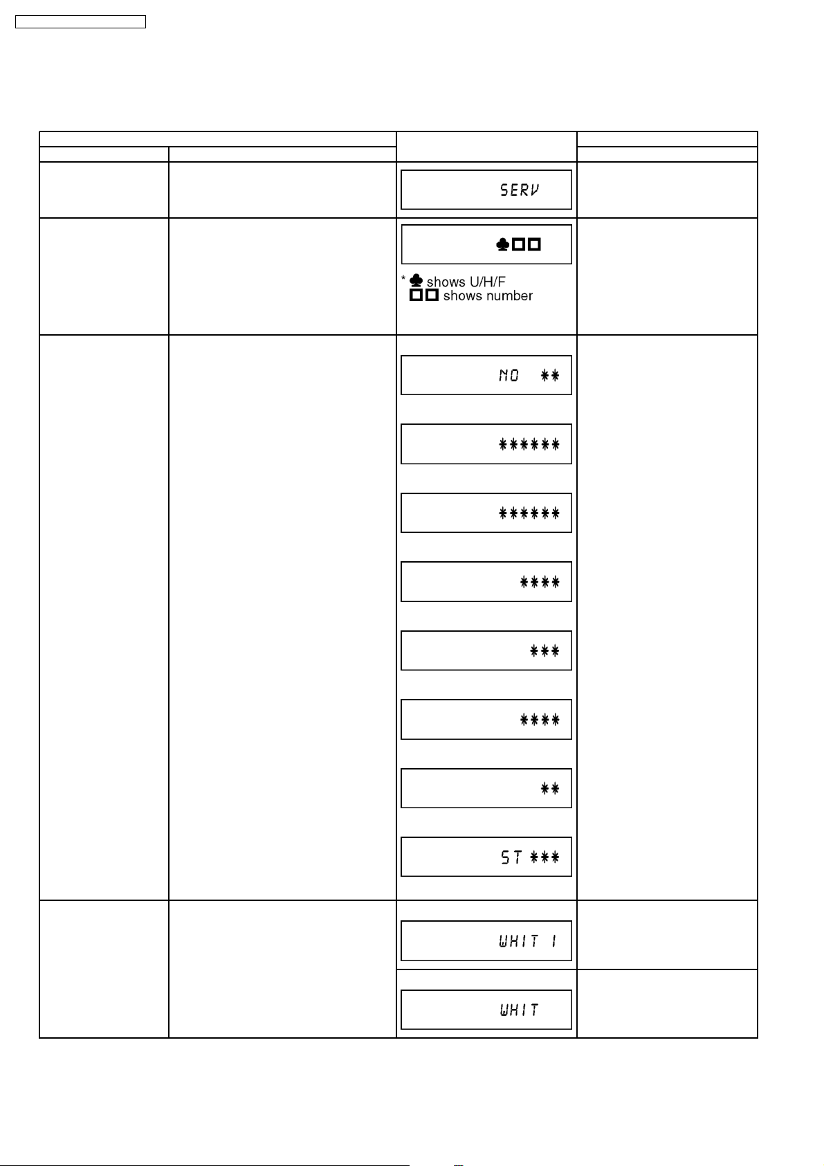
8.1.3. (DVD) SERVICE MODES
Service mode setting: While the power is off, press [STOP], [VHS to DVD COPYING] and [OPEN/CLOSE] simultaneously for five
seconds.
Item FL display Key operation
Mode name Description (Remote controller key)
Release Items Item of Service Mode executing is cancelled. Press [0] [0] or [Return] in service
mode.
Error Code Display Last Error Code of U/H/F held by Timer is
displayed on FL.
*Details are described in “Self-Diagnosis
Functions”.
ROM Version Display 1. Region code
(displayed for 5 sec.)
2. Main firm version
(displayed for 5 sec.)
3. Timer firm version
(displayed for 5 sec.)
4. Drive firm version
(displayed for 5 sec.)
If any error history dose not exist,
[F00] is displayed.
1.
2.
3.
4.
5.
Press [0] [1] in service mode
Press [0] [2] in service mode
5. ROM correction version
(displayed for 5 sec.)
6. VHS Microprocessor version
(displayed for 5 sec.)
7. VHS ROM Correction version
(displayed for 5 sec.)
8. ST Microprocessor version
(left displayed)
White Picture Output White picture is output as component Output
from AV Decoder.
*White picture
(Saturation rate : 100%)
*It is enable to switch Interlace/Progressive
by “I/P switch: [1] [4]”
6.
7.
8.
‘’ ’’ are version displays.
*Initial mode is “Interlace”. Press [1] [1] in service mode.
Switch Interlace/Progressive Press [1] [4] in White Picture
Output mode.
*I/P are switched alternately.
26
Page 27

Item FL display Key operation
Mode name Description (Remote controller key)
Magenta Picture Output Magenta picture is output with Component
*Initial mode is “Interlace”. Press [1] [2] in service mode.
Output from AV Decoder.
*Magenta picture
(Saturation rate: 100%)
*It is enable to switch Interlace/Progressive
by “I/P switch: [1] [4]”
Switch Interlace/Progressive Press [1] [4] in Magenta Picture
Output mode.
*I/P are switched alternately.
DMR-EX95VEG / DMR-EX95VEB
RTSC Return in XP
(A & V)
AV1 input signal is encoded (XP), decoded
(XP) and output decoded signal to external
without DISC recording and DISC playback.
I/P Switch Switch Interlace and Progressive in EE
mode.
*Initial setting is “Interlace”.
*This command is effective during executing
“White Picture Output”, “Magenta Picture
Output” and “RTSC Return in XP (A & V)”
modes.
Audio Mute (XTMUTE) Check whether mute is applied normally by
the timer microprocessor.
Initial mode: EE2/ Interlace/ XP/
Press [1] [3] in service mode.
Audio 48kHz
Switch Interlace/Progressive Press [1] [4] in RTSC Return XP
mode.
*I/P are switched alternately.
Audio 44.1 kHz/ 48 kHz Switch Press [2] [4] in RTSC Return XP
mode.
*48 kHz / 44.1 kHz are switched
alternately.
Initial mode is Interlace
Press [1] [4] in I/P Switch mode.
*I/P are switched alternately.
Switch Interlace/Progressive
Press [2] [1] in service mode.
Audio Mute (XDMUTE) Check whether mute is applied normally by
the Digital P.C.B..
Audio Pattern Output The audio pattern stored in the internal
memory is output
(Lch: 1kHz/-18dB)
(Rch: 400Hz/-18dB)
*Audio sound clock switching operation of
DAC can be confirmed by sub command [2]
[4].
Press [2] [2] in service mode.
Initial mode (Audio 48kHz) Press [2] [3] in service mode.
Audio 44.1kHz/48kHz switching Press [2] [4] in Audio Pattern
Output mode.
*48 kHz / 44.1 kHz are switched
alternately.
27
Page 28
DMR-EX95VEG / DMR-EX95VEB
Item FL display Key operation
Mode name Description (Remote controller key)
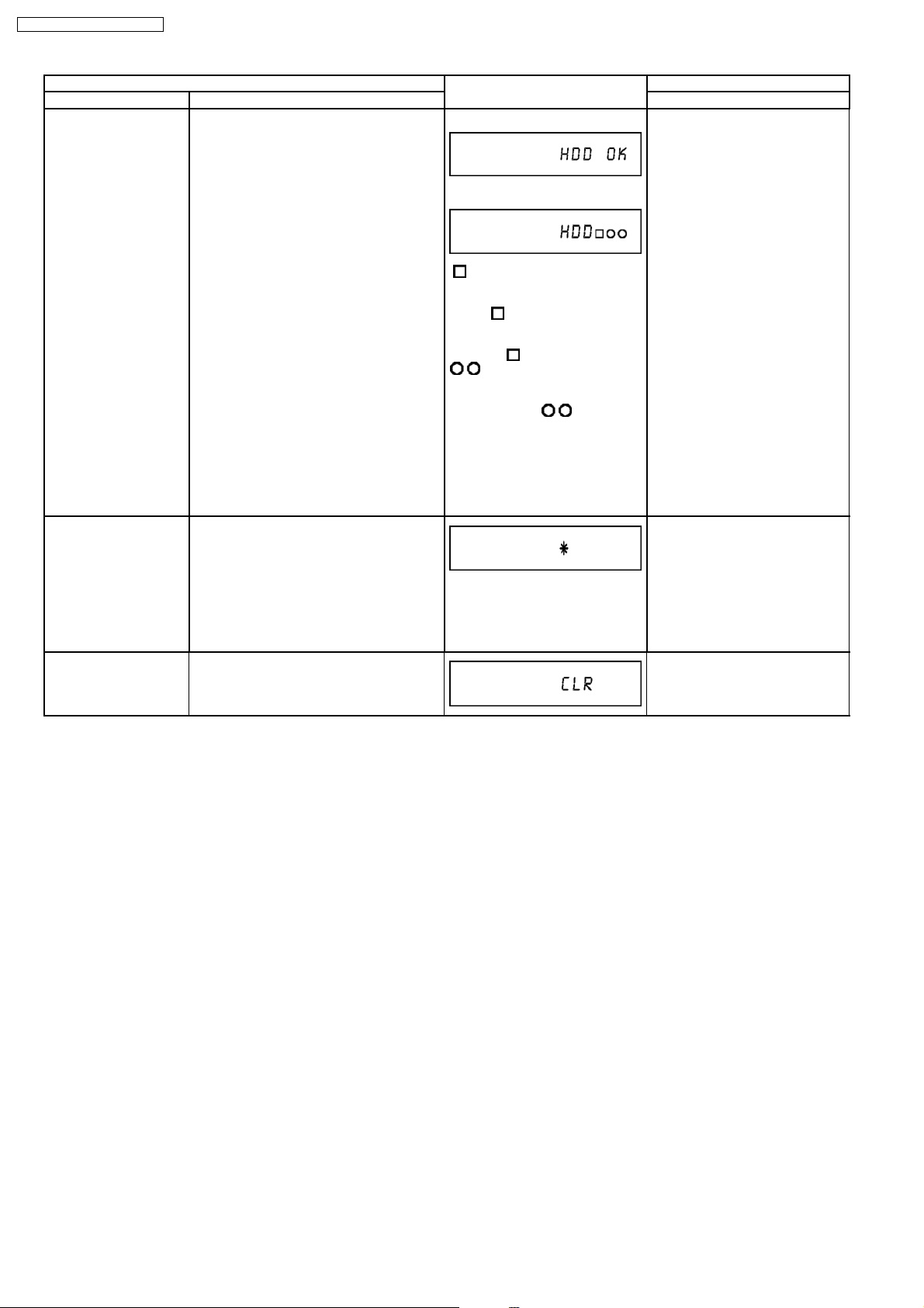
HDD READ inspection Perform a complete read inspection of the
HDD.
Laser Used Time
Check laser used time (hours) of drive.
Indiction
When the HDD is OK
If the HDD is defective
: Judge of Forward rate.
* When normal (Forward rate is 35
Mbps or more and there is no HDD
error):
is Space.
* When Abnormal (Forward rate is
less than 35 Mbps or HDD error
existing):
is X.
: Number of what have
spent time for seeking is over
100ms.
* When normal:
are spaces.
* When Abnormal: Display Number
of what have spent time fore
seeking over 100 ms.
However, if the number is more
than 100, display [XX].
We judge it is normal that the
number is less than 4.
Press [3] [1] in the service mode.
* When canceling the checking
mode while executing, do “forced
power-off”.
Method: Press the “POWER”
button more than 10 seconds.
Press [4] [1] in service mode.
Delete the Laser Used
Time
Laser used time stored in the memory of the
unit is deleted.
●(*****) is the used time display in
hour.
●Laser used time of DVD/ CD in
Playback/Recording mode is
counted.
Press [9] [5] in service mode.
28
Page 29
Item FL display Key operation
Mode name Description (Remote controller key)
RAM Drive Last Error RAM Drive error code display.
*For details about the drive error code, refer
to the Service Manual for the specific RAM
Drive.
1. Error Number is displayed for 5
seconds.
Press [4] [2] in service mode.
When “INFO******” is being
displayed, past 19 error histories
can be displayed by pressing [0]
[1] - [1] [9]
2. Time when the error has
occurred is displayed for 5
seconds.
DD: Day
hh: Hour
mm: Minute
3. Last Drive Error (1/2) is
displayed for 5 seconds.
4. Last Drive Error (2/2) is
displayed for 5 seconds.
DMR-EX95VEG / DMR-EX95VEB
Delete the Last Drive
Error
Delete the Last Drive Error information
stored on the DVD RAM-Drive.
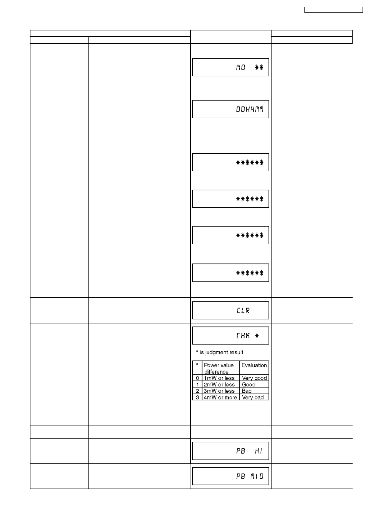
Laser power confirmation Drive state is judged based on difference
between laser power value at shipping and
present laser power value.
5. Error occurring Disc type is
displayed for 5 seconds.
6. Disc Maker ID is displayed for 5
seconds.
In case that the maker cannot be
identified, display is black out.
7. Factor of Drive Error occurring is
left displayed
Press [9] [6] in service mode.
1. Insert DVD-RAM disc
into RAM Drive in service
mode. (Other media are
assumed to be noncorrespondence.)
2. Press [4] [4].
Turn on all FL/LEDs All segments of FL and all LEDs are turned
on.
PB HIGH Signal Output 8 pin of AV 1 Jack (PB HIGH terminal) is
High (approx. 11V DC).
PB MIDDLE Signal
Output
8 pin of AV 1 Jack (PB HIGH terminal) is
Middle (approx. 5.5V DC)
If DVD-RAM disc in not inserted,
[NO DISC] is displayed.
If power value study was filed,
[ERROR] is displayed.
All segments are turned on. Press [5] [1] in service mode.
Press [5] [2] in service mode.
Press [5] [3] in service mode.
29
Page 30
DMR-EX95VEG / DMR-EX95VEB
Item FL display Key operation
Mode name Description (Remote controller key)
Front connection
inspection
Press all front keys and check the
connection between Main P.C.B. and Front
key Switches.
(1) Each time a key is pressed,
segment turned on increases one
by one.
(2) Total umber of keys that have
been pressed.
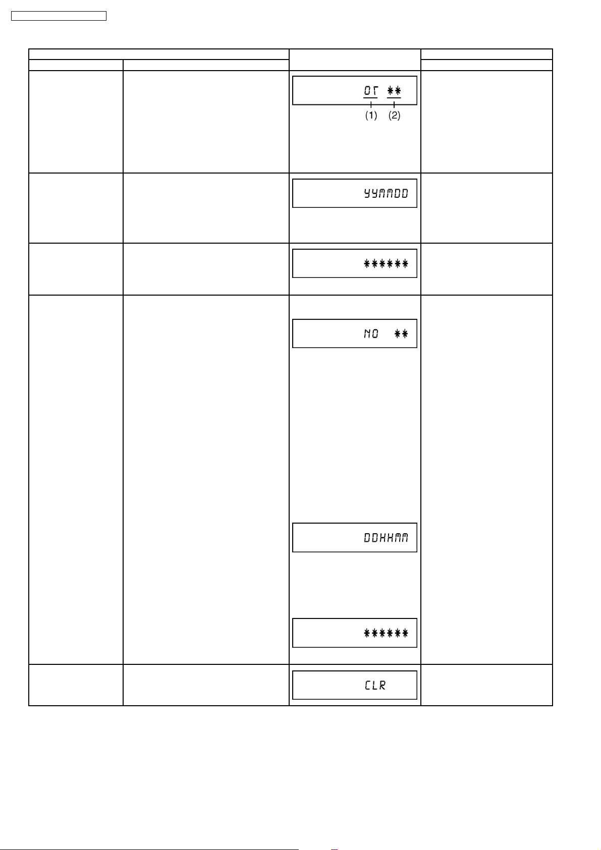
Production Date Display Display the date when the unit was produced.
YY: Year
MM: Month
DD: Day
Display the accumlated
Display the accumulated unit´s working time.
working time
(Indicating unit: Second)
Display the Error History Display the Error History stored on the unit. Display reason of error for
5 seconds.
Press [5] [4] in service mode.
Press [6] [1] in service mode.
Press [6] [4] in service mode.
Press [6] [5] in service mode.
Then press [0] [1] ~ [1] [9], the
past 19 error histories are
displayed.
01:
Defect of Digital P.C.B.
(AV DEC / MAIN CPU)
02:
Defect of RAM Drive.
03:
Defect of Disc.
04:
Defect of Digital P.C.B. or
Communication Error.
05:
Defect of Digital P.C.B.
(AV DEC / MAIN CPU)
06:
Defect of HDD.
Display the time when the error
has occurred for 5 seconds.
DD: Day
hh: Hour
mm: Minute
Accumulated working time till
occuring of the error is left
displayed.
Delete the Error History Delete Error History information stored on
the unit.
(Indicating unit: Second)
Press [9] [7] in service mode.
30
Page 31

Item FL display Key operation
Mode name Description (Remote controller key)
SD card WRITE check Check SD card WRITE function with SD
slot.
When the WRITE check is OK.
Insert a SC card to SD card slot,
and press [7] [4] in service mode.
* Insert SD card while the power is
off.
* Check for [CARD SD] display on
When the WRITE check is NG.
the FL display and go on the
procedure.
*Note:
The image stored in the SD
card will be erased.
AV4(V)/AV1(RGB) I/O
Setting
Set input to AV4 (V) and set output to AV1
(RGB) for I/O checking
Press [8] [0] in service mode.
DMR-EX95VEG / DMR-EX95VEB
AV2(Y/C)/AV1(V) I/O
Setting
AV2(V)/AV1(Y/C) I/O
Setting
AV2(RGB)/AV1(V) I/O
Setting
Set input to AV2 (Y/C) and set output to
AV1 (V) for I/O checking
Set input to AV2 (V) and set output to AV1
(Y/C) for I/O checking
Set input to AV2 (RGB) and set output to
AV1 (V) for I/O checking
P50(H) Output Timer Microprocessor IC9704-76 output
High signal for AV1-pin 10 passing through
inverter (approx. 0V DC at AV1-pin 10).
P50(L) Output Timer Microprocessor IC9704-76 output Low
signal for AV1-pin 10 passing through
inverter (approx. 4.4V DC at AV1-pin 10).
When OK.
When NG.
When OK.
When NG.
Press [8] [1] in service mode.
Press [8] [2] in service mode.
Press [8] [3] in service mode.
Press [8] [4] in service mode.
Press [8] [5] in service mode.
Tray OPEN/CLOSE Test The RAM drive tray is opened and closed
repeatedly.
Press [9] [1] in service mode
*When releasing this mode, press
the [POWER] button of Remote
Controller more than 10 seconds.
“*” is number of open/close cycle
times.
Error code initialization Initialization of the last error code held by
Press [9] [8] in service mode.
timer (Write in F00)
Initialize Service Last Drive Error, Error history and Error
Press [9] [9] in service mode.
Codes stored on the unit are initialized to
factory setting.
Finishing service mode Release Service Mode. Display in STOP (E-E) mode. Press power button on the front
panel or Remote controller in
service mode.
31
Page 32

DMR-EX95VEG / DMR-EX95VEB
8.2. (VHS) SELF-DIAGNOSIS AND SPECIAL MODE SETTING
8.2.1. (VHS) SPECIAL MODES SETTING
Item FL display Key operation
Mode name Description Front Key
Tracking Center Tape Tracking is adj usted to center
FIX position.
VHS Service Mode In order to make service easy, a part of
inside information of a microprocessor
is displayed on FIP.
*Details are described in
"VHS Service Mode".
No display. During PLAYBACK, press [VHS CH
UP] and [VHS CH DOWN] keys
simultaneously.
Press [STOP], and [EJECT] keys
simultaneously for three seconds
when power is off.
Set Drive to VHS.
Releasing EXT LINK &
Timer Program
Eject Ejecting Cassette Tape No display. While in other than Timer REC
Releasing Continuation EXT LINK &
Continuation Timer Program
No display. While in EXT LINK or Timer REC
mode, press [VHS STOP] key for 3
seconds.
mode, press [STOP] key for 3
seconds or press [STOP] key of the
Remote Controller for 3 seconds in
VHS mode.
8.2.2. (VHS) SERVICE MODES
(Service Mode Setting)
1. When power is OFF, press [STOP] and [EJECT] keys simultaneously for 3 seconds to into Service Mode and
set Drive to VHS.
2. In Service Mode, press [STOP] and [EJECT] keys simultaneously to add Service Number.
Service Mode
Number
0 Indication for the
1 Indication for the
2 Indication for the
3 Self-diagnosis
4 Self-diagnosis
5 Self-diagnosis
6 Indication for the
Contents Contents of Indication on minute Contents of Indication on second Remarks
inner data of
IC6001
inner data of
IC6001
inner data of
IC6001
history (1st)
history (2nd)
history (3rd)
inner data of
IC6001
VHS mode
(Real time)
Tape beginning and ending
detection data (Real time)
00: Both tape beginning and
ending have not been detected
01: Tape ending is detecting now
02: Tape beginning is detecting
now
03: Both tape beginning and
ending are detecting now
Mechanism position (Real time) Ordering for the Motors (Real time) The following functions are
0L: EJECT position
02: DOWN position
03: RREW position
04: LOAD position
05: REV position
06: PLAY position
07: POFF position
08: STOP_R position
09: STOP_F position
0- : FF/REW position
0_ : Intermediate between each
positions
1st history of error number "- -" is displayed.
2nd history of error number "- -" is displayed
3rd history of error number "- -" is displayed
Servo data (4 digits)
(Real time)
Process number of the mechanism
movement
(Real time)
Key code
(Real time)
Indicate the receiving code when
the key of VCR or remote
controller being operated.
0*, 2*: CYL off,
CAP off
1*: CYL off,
CAP on (fwd)
3*: CYL off,
CAPon (rev)
8*, A*: CYL on,
CAP off
9*: CYL on,
CAPon (fwd)
B*: CYL on,
CAP on (rev)
*0: Motor off
*1:Loading
*2: Unloading
*3: Break (Load + Unload)
prohibited to operate the
mechanism without cassette tape.
●Tape beginning and ending
detection.
●Reel lock detection
●Tape detection and tape position
detection
Press the EJET key for over 3
seconds in this mode, and then the
VCR is shifted into the special
modes, such as PG Adjustment,
Model Code Setting, and so on.
The orders for the motors are
asfollows.
32
Page 33

DMR-EX95VEG / DMR-EX95VEB
Service Mode
Number
7 Manual mechanism
Contents Contents of Indication on minute Contents of Indication on second Remarks
operation
Mechanism position (Real time) Ordering for the Motors Press the following key;
0L: EJECT position
02: DOWN position
03: RREW position
04: LOAD position
05: REV position
06: PLAY position
07: POFF position
08: STOP_R position
09: STOP_F position
0- : FF/REW position
0 _: Intermediate between each
positions
0*, 2*: CYL off,
CAP off
1*:CYL off,
CAP on (fwd)
3*: CYL off,
CAPon (rev)
8*, A*: CYL on,
CAP off
9*: CYL on,
CAPon (fwd)
B*: CYL on,
CAP on (rev)
*0: Motor off
*1:Loading
*2: Unloading
*3: Break (Load + Unload)
PLAY key: Loading
STOP key: Unloading
8.2.3. (VHS) SELF-DIAGNOSIS FUNCTIONS
This model has a self-diagnosis. If the VHS section detects trouble during installation or during use, the power is automatically
turned off or become power-save mode and it is memorized into the EEPROM (IC9705) as error code of two-digit number. It’s
memorized error code can be displayed in "second" display portion (the last 2 digits of the FIP) by placing the unit is Service Mode
Number 2 when turning on the Service Information Display as for example "01" or "02" etc. as below. If a second error occurs, the
most recent error will be memorized and can be displayed in Service Mode Number 2. It can be memorized until 3 self-diagnosis
histories in maximum.
In order to erase the memorized error code, press STOP and EJECT buttons on the Front Panel simultaneously over 5 seconds
during turning on Service Information Display mode.
8.2.3.1. MEMORY OF THE SELF-DIAGNOSIS HISTORY
*This is effective only in Service Mode 3, 4, 5.
8.2.3.1.1. ERROR NUMBERS AT A GLANCE
Memory No. (Error Code) Reason
01 The cylinder could not be started. (Error of the cylinder or the cylinder driver.)
02 The CAP FG could not be detected.
03 Mechanism lock during without the unloading and the cassette-up.
04 Mechanism lock during unloading
05 S-reel pulse cannot be detected during unloading. (Error of the S-reel circuit or the Capstan circuit)
06 Mechanism lock during the Cassette-up.
09 Communication error between VHS Microprocessor (IC6001) and Timer Microprocessor (IC9704).
15 S-reel pulse cannot be detected when a cassette tape is inserted.
16 Detection of the Cylinder lock during the constant rotation
17 Detection of S-reel lock during the constant tape running
18 Detection of T-reel lock during the constant tape running
2*
Refer to following table
80 An exceptional ejection depends on a accidental error
Note:
2* is as follows.
20 NG1 in the PG Shifter Automatic Adjustment (The cylinder rotation is unstable during the automatic adjustment.)
21 NG2 in the PG Shifter Automatic Adjustment (The vertical sync signal is lacked while over 5 seconds on the alignment tape.)
22 NG3 in the PG Shifter Automatic Adjustment (The installing position of Heads to the cylinder is our of specification.
23 NG4 in the PG Shifter Automatic Adjustment (The servo is not locked to the cylinder for more than 10 sec.)
(Error of the S-reel circuit or the Capstan circuit)
An error while the PG Automatic Adjustment
8.2.3.1.2. MEMORY FOR THE SELF-DIAGNOSIS HISTORY
3. The self-diagnosis result is memorized the state of the moment of detecting.
4. There are the histories from number 1 to number 3.
5. The latest error is memorized on history number 1, and then the old histories are shifted to the history number 2 and 3.
The error code memorized in the history number 2 and 3 is over-written by shift.
4. If the latest error is the same with the history number 1 (2nd-latest), it is not memorized.
(The same error code is not memorized in succession)
33
Page 34

DMR-EX95VEG / DMR-EX95VEB
8.2.3.1.3. CLEAR FOR THE SELF-DIAGNOSIS HISTORY
1. Press STOP and EJECT buttons simultaneously over 5 seconds during turning on Service Information Display mode.
8.2.3.1.4. INDICATION OF THE SELF-DIAGNOSIS HISTORY
The self-diagnosis histories can be indicated on the FIP with Service Mode number 3 to 5.
The procedure of service mode setting and indication format are the same as usual.
9 SERVICE FIXTURE AND TOOLS
Part Number Description Pcs Compatibility
RFKZ03D01K Lead Free Solder (0.3 mm / 100 g Reel) 1 Same as ES15
RFKZ06D01K Lead Free Solder (O.6 mm / 100 g Reel) 1 Same as ES15
RFKZ010D01 Lead Free Solder (1.0 mm / 100 g Reel) 1 Same as ES15
RFKZ0316 Solder Remover (Lead free 10 W temperature Solder / 180 g) 1 Same as ES15
RFKZ0328 Flux 1 Same as ES15
RFKZ0329 Bottle of Flux 1 Same as ES15
JZS0484 Eject Pin 1 Same as ES15
Part Number Description Pcs Compatibility
RFKZ0240 Extension Cable (Main P.C.B. - Power & Digital I/F P.C.B. / 19 pin) 2 Same as ES75V
RFKZ0327 Extension Cable (Main P.C.B. - Power & Digital I/F P.C.B. / 15 pin) 1 Same as ES40V
RFKZ0323 Extension Cable (Main P.C.B. - Power & Digital I/F P.C.B. / 9 pin) 1 New
RFKZ0365 Extension Cable (Power Digital I/F P.C.B. - Digital P.C.B. / 64 pin) 1 Same as ES35
RFKZ0239 Extension Cable (to Front Jack P.C.B. and FL P.C.B. / 10 pin) 4 Same as E75V
RFKZ0260 Extension Cable (Power Digital I/F P.C.B. - Digital P.C.B. / 88 pin) 1 Same as EH50 series
RFKZ0366 Extension Cable (HDMI P.C.B. - Digital P.C.B. / 40 pin / 500 mm) 1 Same as EH55 / EH56 series
(for VHS)
Part Number Description Pcs Compatibility
VFJ8125H3F PAL VHS Alignment Tape 1 Same as E75V
VFK0329 Post Adjustment Screwdriver 1 Same as E75V
VFK0330 Fine Adjustment Gear Driver 1 Same as E75V
34
Page 35

10 ASSEMBLING AND DISASSEMBLING
10.1. DISASSEMBLY FLOW CHART
The following chart is the procedure for disassembling the casing
and inside parts for internal inspection when carrying out the servicing.
To assemble the unit, reverse the steps shown in the chart below.
DMR-EX95VEG / DMR-EX95VEB
10.2. P.C.B. POSITIONS 10.3. CAUTION WHILE INSERTING
CASSETTE TAPE WHEN
DISASSEMBLING THE UNIT
NOTE:
Video Cassette might not enter when a strong lighting is
applied to VHS Mechanism when Video Cassette is
inserted. Please weaken the lighting or cover with the top
panel etc.
35
Page 36

DMR-EX95VEG / DMR-EX95VEB
10.4. TOP CASE
1. Remove the 4 screws (A) and 3 screws (B).
2. Slide the Top Case for rear direction slightly, and open the
both ends at rear side of the Top Case a little and lift up the
Top Case for the direction of the arrows.
10.5. FRONT PANEL
1. Remove one screw (A).
2. Unlock tab (A) and tab (B) simultaneously.
3. Unlock tab (C) and tab (D) simultaneously.
4. Unlock 2 tabs (E) respectively and pull out Front Panel with
connector slightly.
36
Page 37

DMR-EX95VEG / DMR-EX95VEB
Note:
When attaching Front Panel, in order to hook Cassette
Door Opener Lever to Cassette Door, push up cassette
door in the direction of arrow and insert a front panel.
10.7. REAR PANEL
1. Remove Screws (A), Screw (B) and (C)
and Fan Connector.
2. Unlock 2 Locking Tabs (A) and lift up HDD out of the
Locking Tab (B) inside Rearpanel, to remove Rear Panel
without Fan Motor.
3. Attention when inserting Rear Panel:
Don’t shut the Fan Cable between Rear Panel
and Chassis.
Check that the Locking Tabs on both sides on
the Rear Panel snap into the holes of the Chassis.
Note:
When attiching Front Panel push up the Earthspring on
Top of the DV IN Connector.
10.6. FRONT JACK P.C.B. &
FL DRIVE P.C.B.
1. Remove one 6 screws (A) to remove FL Drive P.C.B.
2. Remove 3 screws (B) and unlock the Locking Tab (B) to
remove Front Jack P.C.B.
37
Page 38

DMR-EX95VEG / DMR-EX95VEB
10.8. HARD DISC DRIVE
NOTE:
After replacing HDD, "UNFORMAT" indication is displayed,
then HDD must be formatted.
After that, programme in HDD will be lost.
1. Remove 2 screws on Rear Panel
2. Remove 1 screw on HDD Angle
3. Remove FFC HDD Data Cable from Atapi Connector
4. Lift up HDD
Note:
When you lift up VCR Mechanism Unit, because
connections of P2501 and P3001 are tight,
pay attention to that.
10.9. FAN MOTOR
1. Remove the Fan Connector.
2. Remove 2 Screws to remove Fan Motor.
10.10. VCR MECHANISM UNIT
10.10.1. CAUTION FOR ATTACHING VCR
MECHANISM UNIT
1. Because Position SW should be set to "Eject Position",
refer to fig.(A) and set the position switch so that the boss
and arrow mark come on a straight line.
2. Attach VCR Mechanism Unit so that Boss of Position SW is
put into long hole of Main Cam Gear, refer to Fig. (B).
1. Disconnect 3 Connectors (P1531, P2501 and P4002).
2. Remove 3 black Screws (A), Screw (B), Screw (C)
and Screw D).
3. Lift up VCR Mechanism Unit perpendicularly so to
disconnect Connectors (P2571 and P3001).
38
Page 39

DMR-EX95VEG / DMR-EX95VEB
10.11. MAIN P.C.B.
1. Disconnect 3 Connectors.
2. Remove 3 Screws and remove Main P.C.B.
10.13. DVD-RAM DRIVE / DIGITAL
P.C.B. MODULE
NOTE:
After replacing RAM/Digital P.C.B. Module,
FORMAT of HDD is unnecessary.
CAUTION:
The DVD-RAM Drive and the Digital P.C.B. have
to be replaced together as one Module.
If the Module is changed the DVD-RAM Drive has to
be re-aligned because the aligment data for the
DVD-RAM Drive is stored in the Digital P.C.B.
1. Remove 3 Screws.
2. Lift up DVD-RAM Drive slightly.
10.12. TUNER
1. Remove the solders.
2. Pull out the Tuner from Main P.C.B.
3. Disconnect FFC from Digital P.C.B.
39
Page 40

DMR-EX95VEG / DMR-EX95VEB
4. Remove 4 Screws and DVD Angle.
5. Disconnect FFC.
6. Remove 4 Screws from Digital P.C.B.
7. Pay attention while pulling out Digital P.C.B.
to disconnect Connector (A).
NOTE:
When inserting Digital P.C.B. confirm correct position of
Guide Pins.
10.14. SD/DV IN P.C.B.
1. Remove 2 Screws.
2. Pull out the DV IN P.C.B. backwards.
CAUTION:
When replacing the Module, pay attention to inserting FFC,
and be careful to do not touch surface of CSP ICs. If you
have touched surface of CSP IC, clean up with alcohol and
so on to prevent oxidation.
40
Page 41

10.15. POWER & DIGITAL I/F P.C.B.
NOTE:
After replacing Power & Digital I/F P.C.B., "UNFORMAT"
indication is displayed, then HDD must be formatted.
After that, programme in HDD will be lost.
CAUTION:
The earth springs has to contact the Metalchassis.
DMR-EX95VEG / DMR-EX95VEB
1. Remove Rear Panel and disconnect 3 Connectors.
2. Remove the 6 Screws and DVD Angle (A) and (B).
3. Remove Power & Digital I/F P.C.B.
NOTE:
When inserting P.C.B. confirm correct positions
of Guide Pins.
41
Page 42

DMR-EX95VEG / DMR-EX95VEB
10.16. BACK END P.C.B.
1. Pull out the Back End P.C.B. in direction of the arrow.
10.17. HDMI P.C.B.
1. Remove Screw on backside of Rear Panel.
2. Pull out the HDMI P.C.B. in the direction of the arrow.
42
Page 43

11 MEASUREMENTS AND ADJUSTMENTS
11.1. SERVICE POSITIONS
11.1.1. CHECKING AND REPAIRING OF POWER & DIGITAL I/F P.C.B.
CAUTION:
Before repairing of Power & Digital I/F P.C.B. read and observe “CAUTION FOR DIVX” (NEW FEATURE) first.
1. Top Case
•
• Remove 4 Screws (A) on the side and 3 Screws (B) on the rear side.
• •
•
• Remove Top Case.
• •
2. Front Panel
•
• Remove one Screw (A) on center.
• •
•
• Unlock 2 Locking Tabs (A), (D) on Front Panel side and 2 Locking Tabs (B), (C) on Front Panel topside.
• •
•
• Unlock 2 Locking Tabs (E) on Front Panel bottom side and remove Front Panel.
• •
3. Rear Panel without Fan Motor
•
• Remove Screws (A) and (B) on Rear Panel and Screw (C) from HDD Angle.
• •
•
• Unlock 2 Locking Tabs on the sides and remove Rear Panel.
• •
4. Hard Disc Drive
•
• Remove Power Cable, FF Cable from HDD and HDD.
• •
5. DVD RAM Drive
•
• Remove 3 Screws.
• •
•
• Lift up DVD RAM Drive and remove Cable from Digital P.C.B. and remove DVD RAM Drive with P.C.B. Barrier
• •
•
• Remove 4 Screws, FF Cable (HDMI) and DVD Bracket
• •
6. Digital P.C.B.
•
• Remove 4 Screws from Digital P.C.B., FF Cable from SD/DV IN Card P.C.B. and remove Digital P.C.B.
• •
7. Power & Digital I/F P.C.B.
•
• Disconnect 4 Connectors.
• •
•
• Remove 5 Screws from DVD Angle (A) and DVD Angle (B).
• •
•
• Remove 3 Screws from P.C.B.
• •
•
• Lift up Power & Digital I/F P.C.B. together with DVD Angle (R) and (F).
• •
•
• Connect all Parts and put it together upside-down.
• •
•
• Connect Extension Cables:
• •
−
− between Main P.C.B. and Power Digital I/F P.C.B. : RFKZ0327 and RFKZ0240 (2x)
− −
−
− between Main P.C.B. and Power Digital I/F P.C.B. : RFKZ0323
− −
−
− between Main P.C.B. and Front Jack P.C.B.: RFKZ0239
− −
−
− between Main P.C.B. and FL Drive P.C.B.: RFKZ0239
− −
−
− between Power & Digital I/F P.C.B. and FL Drive P.C.B.: RFKZ0239 (2x)
− −
DMR-EX95VEG / DMR-EX95VEB
43
Page 44

DMR-EX95VEG / DMR-EX95VEB
11.1.2. CHECKING AND REPAIRING OF MAIN P.C.B.
1. Top Case
•
• Remove 4 Screws (A) on the side and 3 Screws (B) on the rear side and remove Top Case.
• •
2. Front Panel
•
• Remove one Screw (A) on center.
• •
•
• Unlock 2 Locking Tabs (A), (D) on Front Panel side and 2 Locking Tabs (B), (C) on Front Panel topside.
• •
•
• Unlock 2 Locking Tabs (E) on Front Panel bottom side and remove Front Panel.
• •
3. Rear Panel without Fan Motor
•
• Remove Screws (A) and (B) on Rear Panel and Screw (C) from HDD Angle.
• •
•
• Unlock 2 Locking Tabs on the sides and remove Rear Panel.
• •
4. Hard Disc Drive
•
• Remove Power Cable, FF Cable from HDD and HDD.
• •
5. VCR Mechanism Unit
•
• Disconnect 4 Connectors (Earth Cable, Loading Motor Cable, 2 FF Cable Connectors) and
• •
remove 1 black Screws (A) and 3 Screws (B), (C), (D).
•
• Lift up VCR Mechanism Unit to remove it.
• •
6. Main P.C.B.
•
• Disconnect 4 Connectors.
• •
•
• Remove 3 Screws and remove Main P.C.B.
• •
•
• Attach VTR Mechanism Unit on to Main P.C.B.
• •
•
• Tighten Screw (C) with Earth Wire and tighten Screw (D) and insert Connectors and 2 FFCs.
• •
•
• Hold Main P.C.B. with VTR Mechanism, put it upside-down.
• •
•
• Connect Power Cable and FF Cable to HDD and put HDD on to the left side.
• •
•
• Connect Extension Cables:
• •
−
− between Main P.C.B. and Power Digital I/F P.C.B.: RFKZ0327 and RFKZ0240 (2x)
− −
−
− between Main P.C.B. and Power Digital I/F P.C.B. : RFKZ0323
− −
−
− between Main P.C.B. and Front Jack P.C.B.: RFKZ0239
− −
−
− between Main P.C.B. and FL Drive P.C.B.: RFKZ0239
− −
−
− between Power & Digital I/F P.C.B. and FL Drive P.C.B.: RFKZ0239 (2x)
− −
44
Page 45

DMR-EX95VEG / DMR-EX95VEB
11.1.3. CHECKING AND REPLACING OF DVD-RAM DRIVE / DIGITAL P.C.B. MODULE
1. Top Case
•
• Remove 4 Screws (A) on side and 3 Screws (B) on rear side.
• •
•
• Remove Top Case.
• •
2. Front Panel
•
• Remove one Screws (A) on center.
• •
•
• Unlock 2 Locking Tabs (A), (D) on Front Panel side and 2 Locking Tabs (B), (C) on Front Panel topside.
• •
•
• Unlock 2 Locking Tabs (E) on Front Panel bottom side and remove Front Panel.
• •
3. DVD-RAM Drive / Digital P.C.B. Module
•
• Remove the 5 Screws.
• •
•
• Lift up and hold the DVD-RAM Drive (together with DVD Angle) slightly.
• •
•
• Remove FF Cable from SD/DV IN Card P.C.B. and FF Cable from HDD.
• •
•
• Remove 4 screws from Digital P.C.B. (pay attention while pulling out Digital P.C.B. to disconnect Connector).
• •
•
• Remove the Digital P.C.B. together with the DVD-RAM Drive and put it beside chassis.
• •
•
• Remove 2 Screws from SD/DV IN Card P.C.B., take P.C.B. out and attach FF Cables back to Digital P.C.B.
• •
•
• Attach the Front Panel back to the Chassis.
• •
•
• Connect Extension Cables:
• •
−
− between Power & Digital I/F P.C.B. and Digital P.C.B. with RFKZ0260 (Red Wire = Pin 1)
− −
−
− between Power & Digital I/F P.C.B. and HDMI P.C.B. with RFKZ0366
− −
CAUTION 1:
The DVD-RAM Drive and the Digital P.C.B. have to be replaced together as one Module.
If the Module is changed the DVD-RAM Drive has to be re-aligned because the aligment data
for the DVD-RAM Drive is stored in the Digital P.C.B.
CAUTION 2:
Before replacing DVD-RAM / Digital P.C.B. Module read and abserve
”CAUTION FOR DIVX” first.
45
Page 46

DMR-EX95VEG / DMR-EX95VEB
11.2. CAUTION FOR REPLACING PARTS
11.2.1. NOTICE AFTER REPLACING DVD-RAM/DIGITAL P.C.B. MODULE
After replacing RAM/Digital P.C.B. Module, FORMAT of HDD is unnecessary.
TM AV1 is displayed after replacing DVD-RAM/Digital P.C.B. Module. Power-off and start-up again.
11.2.2. NOTICE FOR REPLACING PARTS OF VHS MECHANISM
11.2.2.1. REGARDING CHANGE OF PARTS OF VHS MECHANISM
The following parts are not compatible with past R4 Mechanism. Use parts of exclusive use.
Ref. No. Part Name Part Number Pcs
Current Previous
101 RDD CYLINDER ASS’Y VEG1699KIT VEG1648T/VEG1648-DT 1 *1
101-1 FPC HOLDER VMD5464 VMD4983 1
102 CAPSTAN MOTOR VEM0800T VEM0750T 1
105 INTERMEDIATE GEAR VDG1686 VDG1510 1
106 MAIN CAM GEAR VDG1685 VDG1511 1
114 OPENER PIECE VMD5466 VMD4252 1
116 MAIN LEVER VML3934 VML3624 1
117 PINCH CHARGE ARM VML3933 VML3626 1
122 AC HEAD ASS’Y L1AE00000044 L1AE00000036 1
130 T BRAKE ARM VXL3343 VXL3113 1
135 SIDE PLATE L VMD5468 VMD4255 1
136 SIDE PLATE R VMD5469 VMD4254 1
137 CASSETTE HOLDER UNIT VXA8265 VXA7110 1
139 SECTOR GEAR VXA8323 VXA7311 1
*1: Part Number off RDD CYLINDER ASS’Y is different depending on the model.
Capstan Motor (VEM0800T) used for current R4 Mechanism is not compatible with (VEM075oT) of previous R4 Mechanism.
Therefore, confirm part number by Service Manual of individual models and use part of exclusive use.
11.2.2.2. NOTICE FOR REPLACING CAPSTAN MOTOR
VEM0800-1A is printed on capstan motor of replacement part. VEM0800-1B is printed on capstan motor of product.
Thought printed part numbers differ between product and replacement part, VEM0800-1A and VEM800-1B have compatibility.
Replacement Part
“VEM0800-1A” or “VEM0800-1B”
Bottom Bottom
Top Top
Product
“VEM0800-1B”
46
Page 47

11.2.2.3. ITEMS THAT SHOULD BE DONE AFTER REPLACING PARTS
* Note 1:
Resetting object Condition of power Short Terminal
IC6001 POWER ON TL6004 (Reset_L) and TL6002 (GND)
IC9704 POWER ON IC9706-4 (Reset_L) and GND
DMR-EX95VEG / DMR-EX95VEB
* Note 2:
Please will always pass the customer “Warning for Customers Who Use the DivX Video-on-Demand content.” with the product
and get it when you unavoidably exchange EEPROM or P.C.B. including EEPROM (When the product is exchanged,
it is the same.).
You must use print attached to service part (EEPROM or P.C.B. including EEPROM) or must use copy of print below as
“Warning for Customers who use the DivX Video-on-Demand content.”Information needed without fail for the customer for
whom it is used continuing DivX Video-on-Demand Service
to “Manual for the customer” is recorded.
Appendix:* Parts that memorize user’s information are only EEPROM.* The registration of Registration Code is possible for half
a year up to 6 recorders up to 10 recorders a year.
Replacement of EEPROM or P.C.B. including EEPROM spends one of this.
Registration Code is memorized in EEPROM (RFKxxxxxx).
Model without VHS: on Main P.C.B.Model with VHS: on Digital I/F P.C.B. (Power & DVD I/F/P.C.B.)If exchange above P.C.B.
or EEPROM, new registration Code differ from previous Registration Code will be generated.In this case if your customer uses
DivX Video-on-Demand service, he/she will no longer be able to play any content
that he/she purchased under that same registration code.Therefore your customer will need to obtain and register the new
registration code.
47
Page 48

DMR-EX95VEG / DMR-EX95VEB
* Note 3:
PG Shifter Automatic Adjustment Procedure
PROCEDURE F.I.P. DISPLAY
Turn on the Service Mode
1. Set Drive Select to VHS and press the [STOP] and [EJECT] key simultaneously for more than 3 seconds.
Activate the Service Mode 2 (Auto tracking will be turned off).
2. Pressing the [STOP] and [EJECT] key simultaneously twice.
Put it in PG adjustment mode.
3. Press the [EJECT] key for more than 3 seconds.
Set in adjustment No. 1.
4. Press the [CH UP] key once.
Insert the aligment cassette tape (VFM8125H3F)
5. The PG Shifter Adjustment starts automatically.
6. This value displays that PG Adjustment data is memorized in EEPROM
Result Success Cassette tape is ejected automatically.
Error NG1 in the PG Shifter Automatic Adjustment
(The cylinder rotation is unstable during the automatic
adjustment.)
NG2 in the PG Shifter Automatic Adjustment
(The vertical sync signal is lacked while over 5 seconds
on the alignment tape.)
NG3 in PG Shifter Automatic Adjustment
(The installing position of Heads to the cylinder is out of
specification.
NG4 in the PG Shifter Automatic Adjustment
(The servo is not locked to thecylinder for more than 10
sec.)
Exit from Service Mode.
6. Press STOP and EJECT keys simultaneously in 6 times.
* Then the FIP becomes normal indication.
for example
(Normal Indication)
* Note 4:
X-VALUE & LINEARITY (P2 and P3 Posts) Adjustment Procedure
1. Set the Auto Tracking to off.
a. Set Drive Select to VHS and press the [STOP] and [EJECT] keys simultaneously for more than 3 seconds to enter
Service Mode.
b. Press [STOP] and [EJECT] keys simultaneously twice to activate Service Mode 2 and then Auto-Tracking is turned off.
2. Perform the X-VALUE ADJUSTMENT
48
Page 49

DMR-EX95VEG / DMR-EX95VEB
X-VALUE ADJUSTMENT
Caution:
When using alignment tapes without tab for inhibiting REC, press PLAY button after inserting tape.
1. After turning off the Auto tracking, playback the alignment Tape and press [VHS CH UP] and [VHS CH DOWN] keys
simultaneously to adjustment the tracking to FIX value.
2. Adjust A/C Head Base so that the envelope becomes maximum level. (It is described on “5-2. Tape Interchangeability
Adjustment” in “R4 Mechanism” that is separated volume.)
Alignment Tape VFM8125H3F
Test Point of Playback Envelope TW3001 (or TW4502)
LINEARITY ADJUSTMENT
1. After turning off the Auto tracking, playback the alignment Tape and press [VHS CH UP] and [VHS CH DOWN] keys
simultaneously to adjust the tracking to FIX value.
2. Adjust the LINEARITY so that the envelope is flat when moving tracking to (+) and (-) directions.
Alignment Tape VFM8125H3F
Test Point of Playback Envelope TW3001 (or TW4502)
● Main symptoms and Adjustment point
Envelope Post Name Adjustment Method
P2 Post Turn P2 Post counter-clockwise
(Approx. 1/2 revolution)
P2 Post Turn P2 Post clockwise
(Approx. 1/4 revolution)
P3 Post Turn P3 Post clockwise
(Approx. 1/2 revolution)
P3 Post Turn P3 Post counter-clockwise
(Approx. 1/4 revolution)
P2 Post P3 Post Turn P2 Post clockwise
(Less than 1 revolution)
Turn P3 Post counter-clockwise
(Less than 1revolution)
49
Page 50

DMR-EX95VEG / DMR-EX95VEB
50
Page 51

DMR-EX95VEG / DMR-EX95VEB
Note 5:
Please prepare latest firmware updating disc.
*Main Firm is being recorded in HDD, but new HDD has no data.
CAUTION:
- Writing of Main Firm needs 3, 4 minutes.
- Never cut the power of DVD Recorder until writing of Firmware ends.
- Initial settings and contents of reservation will not change if writing is normally completed.
Writing Procedure of Main Firm:
1. Prepare updating disc from firm ware
2. Replace HDD
3. Turn on power of DVD Recorder
4. After [PLEASE WAIT] is displayed on FL., [HDD ERR] is displayed on FL
5. Tray opens automatically
6. Insert updating disc for Firmware and press OPEN / CLOSE key
(If a wrong disc was inserted, [NG DISK] [NO FVU] is displayed on FL.)
7. [LOAD] -> [LD FVU] <- -> [M_Firm] are displayed on FL alternately
8. [MAIN] <- -> [UPD OK] blink alternately and Tray opens. Take out disc (writing was finished)
9. Press Power button to turn off power
10. Press Power button to turn on power
11. [Hello] -> [SELF CHECK] are displayed of FL
12. [UNFORMAT] is displayed on FL
13. After [UNFORMAT] is displayed, message ot request FORMAT is displayed on TV screen
14. Select [YES] and press [ENTER] key to format HDD
(after FORMAT, program in HDD will be lost, but Main firm will not been lost
“Write of the main firm” is completed above
* Drive firm is not updated by above operation. If you wish to update Drive firm, please prepare the disc for latest firmware
update, and write again.
* If the version of the firm you have prepared was same as or laster than has already been written in deck,
“UNSUPPORT” is desplayed on FL.
* In a usual updating of firmware, writing is not performed when the timer reservation standby was not released.
51
Page 52

DMR-EX95VEG / DMR-EX95VEB
11.3. (DVD) STANDARD INSPECTION SPECIFICATION AFTER MAKING
REPAIRS
After making repairs, we recommend performing the following inspection, to check normal operation.
No. Procedure Item to Check
1 Turn on the power, and confirm items pointed out. Items pointed out should reappear.
2 Insert RAM disc. The Panasonic RAM disc should be recognized.
3 Enter the EE (TU IN / AV IN - AV OUT) mode. No abnormality should be seen in the picture, sound or operation.
4 Perform auto recording and playback for one minute using
the RAM disc.
5 If a problem is caused by a VCD, DVD-R, DVD-Video,
Audio-CD, or MP3, playback the test disc.
6 After checking and making repairs, upgrade the firmware to
the latest version.
7 Models with SD Card Slot or DV Input Jack: In case of that
the trouble is caused by SD card and/or DV terminal.
8 Transfer [9][9] in the service mode setting, and initialize the
service settings (return various settings and error
information to their default values. The laser time is not
included in this initialization).
9 When replacing of RAM drive, transfer [9] [5] in the service
mode setting to delete Laser used time.
No abnormality should be seen in the picture, sound or operation.
*Panasonic DVD-RAM disc should be used when recording and
playback.
No abnormality should be seen in the picture, sound or operation.
Make sure that [UPDOK] appears in the FL displays.
*[UNSUPPORT] display means the unit is already updated to newest
same version. Then version up is not necessary.
Models with SD Card or DV Input Jack;1) SD Card: Check to be able to
display and copy the picture.2) DV terminal: Check to be able to record
from DVC.
Make sure that [CLR] appears in the FL display.
After checking it, turn the power off.
Make sure that [CLR] appears in the FL display.
After that, turn power off.
Use the following checklist to establish the judgement criteria for the picture and sound.
Item Contents Check Item Contents Check
Picture
Block noise
Crosscut noise Noise (static, background noise, etc.)
Dot noise The sound level is too low.
Picture disruption The sound level is too high.
Not bright enough The sound level changes.
Too bright
Flickering color
Color fading
Sound
Distorted sound
52
Page 53

12 MISCELLANEOUS
DMR-EX95VEG / DMR-EX95VEB
12.1. ABBREVIATIONS
12.1.1. DVD
INITIAL/LOGO ABBREVIATIONS
A A0~UP
ACLK
AD0~UP
ADATA
ALE
AMUTE
AREQ
ARF
ASI
ASO
ASYNC
B BCK
BCKIN
BDO
BLKCK
BOTTOM
BYP
BYTCK
C CAV
CBDO
CD
CDSCK
CDSRDATA
CDRF
CDV
CHNDATA
CKSL
CLV
COFTR
CPA
CPCS
CPDT
CPUADR
CPUADT
CPUIRQ
CPRD
CPWR
CS
CSYNCIN
CSYNCOUT
D DACCK
DEEMP
DEMPH
DIG0~UP
DIN
DMSRCK
DMUTE
DO
DOUT0~UP
DRF
DRPOUT
DREQ
DRESP
DSC
DSLF
DVD
ADDRESS
AUDIO CLOCK
ADDRESS BUS
AUDIO PES PACKET DATA
ADDRESS LATCH ENABLE
AUDIO MUTE
AUDIO PES PACKET REQUEST
AUDIO RF
SERVO AMP INVERTED INPUT
SERVO AMPOUTPUT
AUDIO WORD DISTINCTION SYNC
BIT CLOCK (PCM)
BIT CLOCK INPUT
BLACK DROP OUT
SUB CODE BLOCK CLOCK
CAP. FOR BOTTOM HOLD
BYPATH
BYTE CLOCK
CONSTANT ANGULAR VELOCITY
CAP. BLACK DROP OUT
COMPACT DISC
CD SERIAL DATA CLOCK
CD SERIAL DATA
CD RF (EFM) SIGNAL
COMPACT DISC-VIDEO
CHANNEL DATA
SYSTEM CLOCKSELECT
CONSTANT LINEAR VELOCITY
CAP. OFF TRACK
CPU ADDRESS
CPU CHIP SELECT
CPU DATA
CPU ADDRESS LATCH
CPU ADDRESS DATA BUS
CPU INTERRUPT REQUEST
CPU READ ENABLE
CPU WRITE ENABLE
CHIPSELECT
COMPOSITE SYNC IN
COMPOSITE SYNC OUT
D/A CONVERTER CLOCK
DEEMPHASIS BIT ON/OFF
DEEMPHASIS SWITCHING
FL DIGIT OUTPUT
DATA INPUT
DM SERIAL DATA READ CLOCK
DIGITAL MUTE CONTROL
DROP OUT
DATAOUTPUT
DATA SLICE RF (BIAS)
DROP OUT SIGNAL
DATA REQUEST
DATA RESPONSE
DIGITAL SERVO CONTROLLER
DATA SLICE LOOP FILTER
DIGITAL VIDEO DISC
INITIAL/LOGO ABBREVIATIONS
G GND COMMON GROUNDING (EARTH)
H HA0~UP
HD0~UP
HINT
HRXW
I IECOUT
IPFRAG
IREF
ISEL
L LDON
LPC
LRCK
M MA0~UP
MCK
MCKI
MCLK
MDATA
MDQ0~UP
MDQM
MLD
MPEG
O ODC
OFTR
OSCI
OSCO
OSD
P P1~UP
PCD
PCK
PDVD
PEAK
PLLCLK
PLLOK
PWMCTL
PWMDA
PWMOA, B
INITIAL/LOGO ABBREVIATIONS
R RE
RFENV
RFO
RS
RSEL
RST
RSV
HOST ADDRESS
HOST DATA
HOST INTERRUPT
HOST READ/WRITE
IEC958 FORMAT DATA OUTPUT
INTERPOLATION FLAG
I (CURRENT) REFERENCE
INTERFACE MODE SELECT
LASER DIODE CONTROL
LASER POWER CONTROL
L CH/R CH DISTINCTION CLOCK
MEMORY ADDRESS
MEMORY CLOCK
MEMORY CLOCK INPUT
MEMORY SERIAL COMMAND CLOCK
MEMORY SERIAL COMMAND DATA
MEMORY DATA INPUT/OUTPUT
MEMORY DATA I/O MASK
MEMORYSERIAL COMMAND LOAD
MOVING PICTURE EXPERTS GROUP
OPTICAL DISC CONTROLLER
OFF TRACKING
OSCILLATOR INPUT
OSCILLATOR OUTPUT
ON SCREEN DISPLAY
PORT
CD TRACKING PHASE DIFFERENCE
PLL CLOCK
DVD TRACKING PHASE DIFFERENCE
CAP. FOR PEAK HOLD
CHANNEL PLL CLOCK
PLL LOCK
PWM OUTPUT CONTROL
PULSE WAVE MOTOR DRIVEA
PULSE WAVE MOTOR OUT A, B
READ ENABLE
RF ENVELOPE
RF PHASE DIFFERENCE OUTPUT
(CD-ROM) REGISTER SELECT
RF POLARITY SELECT
RESET
RESERVE
INITIAL/LOGO ABBREVIATIONS
E EC
ECR
ENCSEL
ETMCLK
ETSCLK
F FBAL
FCLK
FE
FFI
FEO
FG
FSC
FSCK
ERROR TORQUE CONTROL
ERROR TORQUE CONTROL
REFERENCE
ENCODER SELECT
EXTERNAL M CLOCK (81MHz/40.5MHz)
EXTERNAL S CLOCK (54MHz)
FOCUS BALANCE
FRAME CLOCK
FOCUS ERROR
FOCUS ERROR AMP INVERTED INPUT
FOCUS ERROR AMP OUTPUT
FREQUENCY GENERATOR
FREQUENCY SUB CARRIER
FS (384 OVER SAMPLING) CLOCK
53
Page 54

DMR-EX95VEG / DMR-EX95VEB
INITIAL/LOGO ABBREVIATIONS
S SBI0, 1
SBO0
SBT0, 1
SCK
SCKR
SCL
SCLK
SDA
SEG0~UP
SELCLK
SEN
SIN1, 2
SOUT1, 2
SPDI
SPDO
SPEN
SPRCLK
SPWCLK
SQCK
SQCX
SRDATA
SRMADR
SRMDT0~7
SS
STAT
STCLK
STD0~UP
STENABLE
STSEL
STVALID
SUBC
SBCK
SUBQ
SYSCLK
T TE
TIBAL
TID
TIN
TIP
TIS
TPSN
TPSO
TPSP
TRCRS
TRON
TRSON
SERIAL DATA INPUT
SERIAL DATA OUTPUT
SERIAL CLOCK
SERIAL DATA CLOCK
AUDIO SERIAL CLOCK RECEIVER
SERIAL CLOCK
SERIAL CLOCK
SERIAL DATA
FL SEGMENT OUTPUT
SELECTCLOCK
SERIAL PORT ENABLE
SERIAL DATA IN
SERIAL DATA OUT
SERIAL PORT DATA INPUT
SERIAL PORT DATA OUTPUT
SERIAL PORT R/W ENABLE
SERIAL PORT READ CLOCK
SERIAL PORT WRITE CLOCK
SUB CODE Q CLOCK
SUBCODE Q DATA READ CLOCK
SERIAL DATA
SRAM ADDRESS BUS
SRAM DATA BUS 0~7
START/STOP
STATUS
STREAM DATA CLOCK
STREAM DATA
STREAM DATA INPUT ENABLE
STREAM DATA POLARITY SELECT
STREAM DATAVALIDITY
SUB CODE SERIAL
SUB CODE CLOCK
SUB CODE Q DATA
SYSTEM CLOCK
TRACKING ERROR
BALANCE CONTROL
BALANCE OUTPUT 1
BALANCE INPUT
BALANCE INPUT
BALANCE OUTPUT 2
OP AMP INPUT
OP AMP OUTPUT
OP AMP INVERTED INPUT
TRACK CROSSSIGNAL
TRACKING ON
TRAVERSE SERVO ON
INITIAL/LOGO ABBREVIATIONS
V VBLANK
VCC
V BLANKING
COLLECTOR POWER SUPPLY
VOLTAGE
VCDCONT
VIDEO CD CONTROL (TRACKING
BALANCE)
VDD
VFB
VREF
VSS
W WAIT
WDCK
WEH
WSR
X X
XALE
XAREQ
XCDROM
XCS
XCSYNC
XDS
XHSYNCO
XHINT
XI
XINT
XMW
XO
XRE
XSRMCE
XSRMOE
XSRMWE
XVCS
XVDS
XVSYNCO
DRAIN POWER SUPPLY VOLTAGE
VIDEO FEED BACK
VOLTAGE REFERENCE
SOURCE POWER SUPPLYVOLTAGE
BUS CYCLE WAIT
WORD CLOCK
WRITE ENABLE HIGH
WORD SELECT RECEIVER
X´ TAL
X ADDRESS LATCH ENABLE
X AUDIO DATA REQUEST
X CD ROM CHIP SELECT
X CHIP SELECT
X COMPOSITE SYNC
X DATA STROBE
X HORIZONTAL SYNC OUTPUT
XH INTERRUPTREQUEST
X´ TAL OSCILLATOR INPUT
X INTERRUPT
X MEMORY WRITE ENABLE
X´ TAL OSCILLATOR OUTPUT
X READ ENABLE
X SRAM CHIP ENABLE
X SRAM OUTPUT ENABLE
X SRAM WRITE ENABLE
X V-DEC CHIPSELECT
X V-DEC CONTROL BUS STROBE
X VERTICAL SYNC OUTPUT
54
Page 55

12.1.2. VHS
443NT [L]
A. COMP
A. COMPO
A. D.P [L]
A. D/L [L]
A. DEF [S]
A. DEF [S] [L]
A. DUB P [L]
A. DUB [H]
A. ERASE
A. H. SW
A. HEAD [R]
A. HEAD [W]
A. IN [L]
A. IN [R]
A. MUT [H]
A. MUTE [H]
A. OUT [L]
A. OUT [R]
A. RF OUT
A/VS/S. DATA
AC ONLINE
AC. O/EE. H
AFC S C
AFC [S]
AFC. DEF
ARFC OUT
ART. V
ART. V. MM
ART. V/H/N
AT. V/H/N
ATSW/TEST/NOR/SE
AUDIO IN [L]
AUDIO IN [R]
AUDIO OUT [L]
AUDIO OUT [R]
AUDIO SELECT [H]
AUDIO. L
AUDIO. R
AV CNT
AV CTL
AV CTL/S. CLK
AV. C.M.
AVCNT/METER. R
AVSW/METER. L
B MODE. H
B.G.P
BACKUP 5V
BAND. U.E.
BANDVL. D
BI/MI [L]
4.43 NTSC
L
AUDIO COMPONENT SIGNAL
AUDIO COMPONENT SIGNAL
AUDIO DUBBING PAUSE
L
AUDIO DUBBING PAUSE L
AUDIO DEFEAT
AUDIO DEFEAT
AUDIO DUBBING PAUSE
L
AUDIO DUBBING H
AUDIO ERASE
AUDIO HEAD SWITCHING PULSE
AUDIO HEAD (REC)
AUDIO HEAD (PLAY)
AUDIO INPUT (L)
AUDIO INPUT (R)
AUDIO MUTE
H
AUDIO MUTE H
AUDIO OUTPUT (L)
AUDIO OUTPUT (R)
AUDIO RF SIGNAL OUTPUT
AV SW/SERIAL DATA
AC ONLINE
AC ONLINE/EE
H
AFC S CURVE
AFC S CURVE
AFC DEFEAT
AUDIO RF SIGNAL OUTPUT
ARTIFICIAL VERTICAL SYNC SIGNAL
ARTIFICIAL VERTICAL SYNC
SIGNAL MONO MULTI
ARTIFICIAL VERTICAL SYNC
SIGNAL
H/NORMAL
ARTIFICIAL VERTICAL SYNC SIGNAL
TEST/NORMAL/SERVICE
AUDIO INPUT (L)
AUDIO INPUT (R)
AUDIO OUTPUT (L)
AUDIO OUTPUT (R)
AUDIO SELECT
H
AUDIO (L)
AUDIO (R)
AV CONTROL
AV CONTROL
AV CONTROL/SERIAL CLOCK
AV CONTROL MODE
AV CONTROL/LEVEL METER (R)
AV SW/LEVEL METER (L)
B MODE
H
BURST GATE PULSE
BACK UP 5V
BAND U
BAND VL
BILINGUAL/MIX
L
BIL
BIL [L]
BIL. [H]
BIL/M1 [L]
BS CLOCK
BS DATA
BS LCH IN
BS MIX [H]
BS MON [H]
BS MONI [H]
BS RCH IN
BS VIDEO
BS VIDEO/BS1
BS [H]
BS. LEVEL
BS. M [H]
BS/VTR [H]
BUS CLK
BUS LSN
BUS TLK
BUZZER
CAP EC
CAP M GND
CAP. ET
CAP. FG1
CAP. FG2
CAS. SW
CCN
CCP
CHM
CHP
CINEM [L]
CINEMA [L]
CINEMA/MIX
CKL
CKS
CL
CLK
CLK (C.G)
CLOCK. IN
CLP
COL/B/W/NOR
COLOR [H]
CONV
CS
CTL GND
CTL HEAD [
+
]
CTL HEAD [
−
]
CTL [
+
]
CTL [
−
]
CUE BIAS
CURRENT LIM
CYL ET
BILINGUAL
BILINGUAL
L
BILINGUAL H
BILINGUAL L
BS CLOCK
BS DATA
BS L CHANNEL INPUT
BS MIX
H
BS MONITOR H
BS MONITOR H
BS R CHANNEL INPUT
BS VIDEO SIGNAL
BS VIDEO SIGNAL
BS
H
BS LEVEL
BS MONITOR
H
BS/VTR H
BUS CLOCK
BUS LISTEN
BUS TALK
BUZZER
CAPSTAN TORQUE CONTROL
CAPSTAN MOTOR GND
CAPSTAN TORQUE CONTROL
CAPSTAN FG1 PULSE
CAPSTAN FG2 PULSE
CASSETTE SW
PLAYBACK CONTROL SIGNAL (−)
PLAYBACK CONTROL SIGNAL (
+
)
CONTROL SIGNAL (+)
CONTROL SIGNAL (
−
)
CINEMA
L
CINEMA L
CINEMA/MIX
RATCH LOCK
SHIFT LOCK
CLOCK
CLOCK
CLOCK
CLOCK INPUT
CLAMP
COLOUR/BLACK & WHITE/NORMAL
COLOUR H
CONVERTOR
CHIP SELECT
CONTROL GND
CONTROL HEAD (
+
)
CONTROL HEAD (
−
)
CONTROL HEAD (
+
)
CONTROL HEAD (
−
)
CUE BIAS
CURRENT LIMMITER
CYLINDER TORQUE CONTROL
DMR-EX95VEG / DMR-EX95VEB
55
Page 56

CYL GND
D.F.M. REC [H]
D. FM REC [L]
D. GND
D. REC [H]
D4/S. LED
D4/STILLED
DAC [CLK]
DAC/FSCS
DAREC [H]
DATA
DECODER [L]
DECODER [R]
DEW
DEW SNS
DFMRE [H]
E. REC 5V
EC
ECR
EDT TRIG [L]
EDIT [H]
EE [H]
EE [H]/INS [M]
EE. VV. TR
EJECT. PO
EJECT/VDET
ENV. SEL
ENVE. OUT
ENVE. SEL
ENV SELECT
EP [H]
EP/LP [H]
EP/LP/SP
EP/SS [H]
EPROMCS
EX. REC 5V
FF/REW [L]
FG1 IN
FG2 IN
FILTER ADJUSTMENT
FLY ERASE [H]
FLY ON [H]
FLY. E [H]
FM MUT [H]
FM MUTE [H]
FM OUT [L]
FM OUT [R]
FM PACK OUT [L]
FM PACK OUT [R]
FM/BS SEL [L]
FM/BS SEL [R]
FS. CLK
FUL. E [H]
FULL. E [H]
CYLINDER GND
DELAIED FM RECORDING
H
DELAIED FM RECORDING L
DIGITAL GND
DELAYED RECORDING
H
D4/STILL LED
D4/STILL LED
TUNER DAC (CLOCK)
TUNER DAC/FS CHIP SELECT
DELAYED AUDIO RECORDING
H
DATA
DECODER (L)
DECODER (R)
DEW
DEW SENSOR
DELAYED FM AUDIO RECORDING
H
EXCEPT RECORDING 5V
ERROR TORQUE CONTROL
ERROR TORQUE CONTROL
REFERENCE VOLTAGE
EDIT TRIGGER
L
EDIT H
EE H
EE H/INSERT M
EE/VV/TRICK PLAY
EJECT POSITION
EJECT/REVERSE SLOW LOCK
ENVELOPE SELECT
ENVELOPE OUTPUT
ENVELOPE SELECT
ENVELOPE SELECT
LP
H
LP H
LP/SP
LP/SLOW/STILL/STOP
H
EPROM CHIP SELECT
EXCEPT RECORDING 5V
FIRST FORWARD/REWIND
L
FG1 PULSE INPUT
FG2 PULSE INPUT
FILTER ADJUSTMENT
FLYING ERASE HEAD ON
H
FLYING ERASE HEAD ON H
FLYING ERASE HEAD ON H
FM AUDIO MUTE H
FM AUDIO MUTE H
FM OUTPUT (L)
FM OUTPUT (R)
FM PACK OUTPUT (L)
FM PACK OUTPUT (R)
FM/BS SELECT (L)
FM/BS SELECT (R)
FS CLOCK
FULL ERASE HEAD ON
H
FULL ERASE HEAD ON H
FULL. E. 12V
GND [A]
GND [TU]
GND/N. SW. 12V
H. SYNC
H. AMP. SW
H. P <R>
H. P <L>
H. P GND
H. P OUT [L]
H. P OUT [R]
H. SW
HEAD PHONE [L]
HEAD PHONE [R]
HEAD SW
HEATER [
+
]
HEATER [
−
]
HSS
HTR [
+
]
HTR [
−
]
I RFE
ICL
IF
IN SELA1
IN SELA2
IN SELA3
INS L/R [L]
INS. [H]
INSEL A1
INSEL A2
INSERT
INSERT [H]
IO CS
JOG1
JOG S3 LED/FOWRD
JOG/F. LED
JSB [H]
JST. CLCK
JST. CLK
JST. CLOCK
L. OUT
L. CH [H]
L. CH [L]
LED (MAIN)
LED (STEREO)
LED (SUB)
LED CKL
LED CKS
LED DATA
LINE IN 1 [L]
LINE IN 1 [R]
LINE IN 2 [L]
LINE IN 2 [R]
LINE IN V
LINE IN [L]
FULL ERASE 12V
GND (ANALOG)
GND (TUNER)
GND/NON SW 12V
HORIZONTAL SYNC
HEAD AMP SW PULSE
HEAD PHONE (R)
HEAD PHONE (L)
HEAD PHONE GND
HEAD PHONE OUTPUT (L)
HEAD PHONE OUTPUT (R)
HEAD SW PULSE
HEAD PHONE (L)
HEAD PHONE (R)
HEAD SW
HEATER (
+
)
HEATER (
−
)
HORIZONTAL SYNC SIGNAL
HEATER (
+
)
HEATER (
−
)
REFERENCE CURRENT
CONTROL AGC CIRCUIT
INTERMEDIATE FREQUENCY
INPUT SELECT A1 POSITION
INPUT SELECT A2 POSITION
INPUT SELECT A3 POSITION
INSERT Lch/Rch
L
INSERT H
INPUT SELECT A1 POSITION
INPUT SELECT A2 POSITION
INSERT
INSERT
H
INPUT/OUTPUT CHIP SELECT
JOG1
JOG LED/FORWARD LED
JOG LED/FORWARD LED
JSB
H
JUST CLOCK
JUST CLOCK
JUST CLOCK
Lch OUTPUT
Lch
H
Lch L
LED (MAIN)
LED (STEREO)
LED (SUB)
LED SERIAL CLOCK
LED SERIAL CLOCK
LED SERIAL DATA
LINE INPUT 1 (L)
LINE INPUT 1 (R)
LINE INPUT 2 (L)
LINE INPUT 2 (R)
LINE INPUT VIDEO
LINE INPUT (L)
DMR-EX95VEG / DMR-EX95VEB
56
Page 57

LINE IN [R]
LINE OUT [L]
LINE OUT [R]
LP [H]
LPTRI [L]
Lch/A. DUB
M GND
M REG
MAIN OUT
MAIN [L]
MAIN/MONO
MAX IN
MES [H]
MESE [H]
MESE [L]
METER 5V
METER [L]
METER [R]
METER. L/AVS
METER. R/AVC
MI/BI [L]
MIC GND
MIC IN
MIC IN [L]
MIC IN [R]
MIC [H]
MIX [H]
MIX [H]/CINEMA [L]
MIX/CINE
MIX/CINEMA [L]
MN. H/M. L
MN. H/MAI. L
MN2/MES. L
MODE SEL
MODE SW
MODE. S. IN
MODE. S. OUT
MONO [H]
MONO [H]/MAIN [L]
MONO2 [L]
MONO2/MESE [FM(L)]
MOTOR GND
MUTE
N. A. REC [L]
N. SW 12V
N. SW. 5. DET
NICAM
NICAM [L]
NOL [H]
NOR/SOFT [H]
NORMAL [H]
NR BIAS
NTSC [L]
OCH
OUT
LINE INPUT (R)
LINE OUTPUT (L)
LINE OUTPUT (R)
LP
H
LP TRICK PLAY L
Lch/AUDIO DUBBING
MOTOR GND
MOTOR REGULATOR
MAIN OUTPUT
MAIN
L
MAIN/MONAURAL
MAXIMAM INPUT
MESECAM
H
MESECAM H
MESECAM L
LEVEL METER 5V
LEVEL METER (L)
LEVEL METER (R)
LEVEL METER (L)
LEVEL METER (R)
MIX
H/BILIGUAL
MIC GND
MIC INPUT
MIC INPUT (L)
MIC INPUT (R)
MIC
H
MIX H
MIX H/CINEMA SOUND L
MIX H/CINEMA SOUND L
MIX H/CINEMA SOUND L
MONAURAL H/MAIN L
MONAURAL H/MAIN L
MONAURAL 2/MESECAM L
AUDIO MODE SELECT
AUDIO MODE SW
AUDIO MODE SELECT INPUT
AUDIO MODE SELECT OUTPUT
MONAURAL
H
MONAURAL H/MAIN L
MONAURAL 2
MONAURAL 2/MESECAM (FM
L)
MOTOR GND
MUTE
NORMAL AUDIO RECORDING
NON SW 12V
NON SW 5V DETECT
NICAM
NICAM
L
PAL H/4.43 NTSC M/3.58 NTSC
L
NORMAL/SOFT TAPE PLAY H
NORMAL H
NR BIAS
NTSC
L
CONTROL AGC CIRCUIT
OUTPUT
P-OFF [H]
P-OFF [L]
P. FAIL
P. OFF [H]
P. OFF [L]
PAL [H]
PAL [L]/NTSC [H]
PB ADJ OUT
PB OUT
PB. H
PFG
PHOTSN +B
PICT. CNT
PLAY LED/RVS LED
PLAY. PO
PLAY/R. LED
PLY/DEW
POWER OFF [L]
PREROLL [H]
PWRFAIL
R. CH [H]
R. CH [L]
R. ST
R/S/F
RCH [H]
REC 12V
REC CHROMA
REC H
REC IN
REC OUT [L]
REC START
REC VR [C]
REC VR [L]
REC VR [R]
REC Y
REC [H]
REC. C
REC. Y
REC/EE CTL
REEL-T
REEL-S
REGULATOR FILTER
RESET
REV M F/R
REV M V1
REV M V2
REV MOTOR F/R
REV MOTOR V1
REV MOTOR V2
REV MOTOR [
+
]
REV MOTOR [
−
]
REV. M. GND
RF. CHROMA
POWER OFF
H
POWER OFF L
POWER FAILURE DETECT
POWER OFF
H
POWER OFF L
PAL H
PAL L/NTSC H
PLAYBACK ADJUST OUTPUT
PLAYBACK OUTPUT
PLAYBACK
H
PG/FG
PHOTO SENSOR +B
PICTURE CONTROL
PLAY LED/REVERSE LED
PLAY POSITION
PLAY LED/REVERSE LED
PLAY/DEW
H
POWER OFF L
PREROLL H
POWER FAILURE DETECT
Rch
H
Rch L
RESET
REVERSE H/STOP M/FORWARD
L
Rch H
RECORDING 12V
RECORDING CHROMINANCE SIGNAL
RECORDING H
RECORDING INPUT
RECORDING OUTPUT
L
RECORDING START
RECORDING VOLUME (COMMON)
RECORDING VOLUME (L)
RECORDING VOLUME (R)
RECORDING LUMINANCE SIGNAL
RECORDING H
RECORDING CHROMINANCE SIGNAL
RECORDING LUMINANCE SIGNAL
RECORDING/EE CONTROL
REEL PULSE (TAKE-UP)
REEL PULSE (SUPPLY)
REGULATOR FILTER
RESET
REVIEW MOTOR
FORWARD/REVERSE
REVIEW MOTOR V1
REVIEW MOTOR V2
REVIEW MOTOR
FORWARD/REVERSE
REVIEW MOTOR V1
REVIEW MOTOR V2
REVIEW MOTOR (
+
)
REVIEW MOTOR (
+
)
REVIEW MOTOR GND
RF CHROMINANCE SIGNAL
DMR-EX95VEG / DMR-EX95VEB
57
Page 58

RF OUT
RF Y
RF. Y. IN
RF. Y. OUT
ROTAR. SW
ROTARY
RST
RST [L]
Rch/INST
S IN
S OUT
S-PHOTO
S-RL. PLS
S. CLK
S. CLK/AV
S. DATA
S. DATA/A
S. PHOTO
S. TAB [L]
S/P/N
SC IN
SC OUT
SCK SELECT
SEL OUT [L]
SEL OUT [R]
SHUTTLE 1
SIF
SLMUT [H]
SLNID [
+
]
SLNID [
−
]
SLW TR. MM
SLW TR. REF
SNS. GND
SOFT [H]
SOFT [H]/NORMAL
SOLENOID ON [L]
SP [H]
SP/L/SLP
SSS [L]
STEREO LED
STEREO [H]
STEREO [L]
STOP. PO
STOP/5V
STOP1/TAPE SEL
STOP1/PAL:ST
STOP2. PO
STOP2/S-TAB
STREO [H]
SUB BIAS
SUB. SW
SVHS CAS [L]
SW. 5. DET
SYNC [L]
RF OUTPUT
RF LUMINANCE SIGNAL
RF LUMINANCE SIGNAL INPUT
RF LUMINANCE SIGNAL OUTPUT
ROTARY SW
ROTARY SW
RESET
RESET
L
Rch/INSERT
SERIAL DATA INPUT
SERIAL DATA OUTPUT
SUPPLY PHOTO TRANSISTOR
SUPPLY REEL PULSE
SERIAL CLOCK
SERIAL CLOCK/AV
SERIAL DATA
SERIAL DATA
SUPPLY PHOTO TRANSISTOR
SAFETY TAB SW ON
L
SECAM/PAL/NTSC
SERIAL CLOCK INPUT
SERIAL CLOCK OUTPUT
SERIAL CLOCK SELECT
SELECT OUTPUT (L)
SELECT OUTPUT (R)
SHUTTLE 1
SOUND INTERMEDIATE FREQUENCY
INPUT SELECT MUTE H
SOLENOID (
+
)
SOLENOID (
−
)
SLOW TRACKING MONO MULTI
SLOW TRACKING REFERENCE
VOLTAGE
SENSOR GND
SOFT TAPE PLAY
H
SOFT TAPE PLAY H/NORMAL H
SOLENOID ON L
SP H
SP/LP
SLOW/STILL/STOP
STEREO LED
STEREO
H
STEREO L
STOP POSITION
STOP POSITION/5V
STOP1 POSITION/TAPE SELECT
STOP1 POSITION/PAL
STOP 2 POSITION
STOP 2 POSITION/SAFETY TAB SW
STEREO H
SUB BIAS
SUB SW
S-VHS CASSETTE
L
SW 5V DETECT
SYNC
L
SYSCON 5V
SYSTEM
T-PHOTO
T-RL. PLS
T. BUSCLK
T. BUSLSN
T. BUSTLK
T. END [L]
T. PHOTO
TAPE END [L]
TAPE END [L]/CAM
TEST
TPZ
TRIC [L]
TRICK [L]
TRK. ENV
TU. AUDIO
TU. GND
TU. V. IN
TU. VIDEO
TUN NOR IN
TUN R
TUN. AUDIO IN
TUNER 12V
TUNER L
TUNER V IN
TUNER [L]
TUNER [N]
TUNER [R]
TUNER. 12
TUOFF [H]
TV. AUDIO
TV/VTR
TXTON [L]
U. REG45V
UNREG
UNREG19V
V. REF
V. EE [H]
V. EE [L]
VCO REF
VD. IN
VD. OUT
VIDEO EE [L]
VIDEO IN
VIDEO OUT
VM
VM DOWN [L]
VSS
VTR [H]
VTR. 12V
X IN
X OUT
SYSTEM CONTROL 5V
SYSTEM SW
TAKE-UP PHOTO TRANSISTOR
TAKE-UP REEL PULSE
TIMER BUS CLOCK
TIMER BUS LISTEN
TIMER BUS TALK
TAPE END
L
TAKE-UP PHOTO TRANSISTOR
TAPE END
L
TAPE END L/CAMERA PAUSE
TEST MODE
TRAPEZOIDAL WAVE CIRCUIT
TRIC PLAY
L
TRIC PLAY L
AUTO TRACKING ENVELOPE DETECT
TUNER AUDIO
TUNER GND
TUNER VIDEO SIGNAL INPUT
TUNER VIDEO
TUNER NORMAL INPUT
TUNER AUDIO (R)
TUNER AUDIO INPUT
TUNER 12V
TUNER AUDIO (L)
TUNER VIDEO SIGNAL INPUT
TUNER AUDIO (L)
TUNER AUDIO (NORMAL)
TUNER AUDIO (R)
TUNER 12V
TUNER OFF
H
TV AUDIO
TV/VTR
TEXT ON
L
UNREGULATOR 45V
UNREGULATOR
UNREGULATOR 19V
REFERENCE VOLTAGE
VIDEO EE
H
VIDEO EE L
REFERENCE OSCILLATER
VIDEO SIGNAL INPUT
VIDEO SIGNAL OUTPUT
VIDEO EE
L
VIDEO SIGNAL INPUT
VIDEO SIGNAL OUTPUT
MOTOR VOLTAGE
MOTOR VOLTAGE DOWN
L
VERTICAL SYNC SIGNAL
VTR
H
VTR 12V
OSCILLATOR INPUT
OSCILLATOR OUTPUT
DMR-EX95VEG / DMR-EX95VEB
58
Page 59

13 BLOCK DIAGRAM
13.1. POWER SUPPLY BLOCK DIAGRAM
D1101, L1101
L1102
AC-Socket
P1101
250V T2AL
F1101
SURGE
ABSORBER
BRIDGE
RECTIFIER
C1103
HOT COLD
T1101
SW TRANSFORMATOR
7
DMR-EX95VEG / DMR-EX95VEB
IC1101
SW IC
4
11
12
2
4
5
D1D2
VCC
7
GND
8
FB
2
1
Q1101
4
3
13
14
1
2
QR1202
D1203
IC1201
1
IC1202
3
7
IC1203
1
2
IC1204
1
Q1202
1
5
236
4
2
1
7
8
QR1203
Q1204
3
IC1206
6
(Reset)
X_SW5R8V
X_SW12V
P1202
1
2
3
4
DR_12V
DR_5V
HDD_PFAIL_L
X_SW3R8V
DR_12V
DR_12V
DR_GND
DR_5V
59
Q1201
4
QR1201
8
DR_PON_H
DI_PON_H
DMR-EX95VEG
DMR-EX95VEB
POWER SUPPLY
BLOCK DIAGRAM
Page 60

DMR-EX95VEG / DMR-EX95VEB
13.2. SYSTEM CONTROL, SERVO & TIMER BLOCK DIAGRAM
HALL
LOADING
MOTOR
M
CYLINDER
MOTOR
COILS
CAPSTAN
MOTOR
COILS
HALL
+
-
P1531
P1531
PG
COIL
1
2
HALL
(CAPSTANMOTOR DRIVE)
IC0201
A1
15
A2
MOTOR
16
DRIVE
A3
17
22
H3-
23
H3+
H1-
24
H1+
25
H2-
26
H2+
27
VH+
21
(LOADING MOTOR & CYLINDER MOTOR DRIVE)
IC2501
OUT 1
2
OUT 2
4
M1
22
M2
23
M3
25
MOTOR
DRIVE
COM
20
PG+
15
PG-
16
PG OUT
17
DEF
AMP
HALL
POWER
DIFFERENTIAL
AMPLIFIRE
DIFFERENTIAL
AMPLIFIRE
AMP
AMP
PRE-DRIVE
POSITION
SIGNAL
PROCESS
PRE-DRIVE
MOTOR
DRIVE
SIGNAL
GENERATOR
FG/PG
COMPOSER
TORQUE
CONTROL
TORQUE
DIRECTION
SELECT
TL
AMP
EC
AMP
CONTROL
LOGIC
SELECTOR
DIFFERENTIAL
AMPLIFIRE
VM
19
TL
9
EC
10
ED/S
11
DIFFERENTIAL
AMPLIFIRE
-
CAPSTAN
FG
HEAD
+++
FIN
RIN
VCC
5
6
19
P0201
P0201
P0201
P0201
P0201 P2571
+5V
2
5
6
7
3
P2571
P2571
P2571
P2571
XSW
+12V
TL2502
CAP TL
TL2515
CAP FG
(SYSTEM CONTROL/SERVO/TIMER)
IC6001
CURRENT LIMIT
11
CAP ET
76
CAP R/F
74
86
FG. AMP. OUT
87
FG. AMP. IN
29
LOADING
28
UNLOADING
OREF91
N
CTL AMP REF96
CYL ET
7714
PFG9018
H
12MHz IN 38
12MHz OUT 39
L
H
H
PON 75
H
TIMER BUS DATA OUT 68
TIMER BUS DATA IN 69
TIMER BUS CLK 70
X6001
(12MHz)
AD 5V5V(D) 37
IC6201
(RESET)
4 OUT
+6V
5
TL600434RESET
TL6002
IC6302
(SWITCHING REG.+5V)
1
15TIMER CS
INOUT 4
ON
3
TO
IC3002 , QR4501
5
X SW+5.8V+5V
P6001
P6001
P6001
FROM
POWER
P9101P6001
12
P9101
8
7
6
P9101
P9101
TO/FRO M
POWER &
DIGITALI/F
P. C . B .
CONTROL
MODE
SW
S1532
Q1501
TAKE-UP
PHOTO
SENSOR
P4002HEAD
P4002
1
2
3
4
5
CTL HEAD(-)
SW1
SW2
SW3
SW4
TL24
TL23
94
CTL HEAD(+)
95
EX.FF/REW
82
PB CTL OUT
97
POSITION SW133
32 POSITION SW2
POSITION SW331
30 POSITION SW4
8 T.PHOTO
7 S.PHOTO
26 SAFETY TAB
79 S.REEL
80 T.REEL
P9101P6001
4
L
PS6001
PS6002
PS6002
PP7503
33
PP4801
44
PP4801
11
14REMOCON
VHS KEY 2 6
L
VHS KEY 1 5
IC7502
(REMOTE CTL.RECEIVER)
1IR
S7804 S7805 S7806
EJECT REW CH DOWN
AD +5V3
S7803S7802S7801
FRONT JACK P.C.B.
CH-UPFFPOWER
5
6
SW1
SW2
SW3
SW4
+5V
D1501
SENSOR
LED
Q1502
SUPPLY
PHOTO
SENSOR
S1531
SAFETY
TAB SW
+5V
IC1501
(T-REELSENSOR)
21
4
IC1502
(S-REEL SENSOR)
3423
1
TW2002
PB CTL
DMR-EX95VEG
DMR-EX95VEB
SYSTEM CONTROL / SERVO & TIMER
BLOCK DIAGRAM
60
Page 61

13.3. AUDIO BLOCK DIAGRAM
:REC SIGNAL :PB SIGNAL
P9703
MIX_LOUT_DM
JK4801
FRONT INPUT JACK
AV3
39
P9703
41
XT_MUTE
IC9704
AUDIO
PP9703
64
(DECODER/EXT)
LINE
(Rch)
LINE
(Lch/MONO)
P4002
4
44
MIX_ROUT_DM
JK3901
21 PIN JACK
AV1
(TV)
AV2
JK3902
21 PIN JACK
IEC OUT
AUDIO IN ch2(R)
2
AUDIO IN ch1(L)
6
AUDIO IN ch2(R)
2
AUDIO IN ch1(L)
6
3
2
1
5
4
TU7801
TUNER
IC3001
98
PP4801
PP4801
TUNER
AUDIO
PS6002
7
7
PS6002
5
5
18SIFOUT
17
1
FROM
DIGITAL
P. C . B .
FROM
DIGITAL
INTERFACE
(FRONT) AV3 Lch
TO
AC HEAD
FROM
DIGITAL
P. C . B .
IC7301
25
SIF
43
MONO IN
DVB- T
BACKEND PCB
Q9302
OUT R
OUT L
19 19
P9103
17
2
1
L
R
Q9303
P6003P9103
P6003
17
IC3901
DAC Rch
56
DAC Lch
64
AV1 Rch
52
AV1 Lch
60
AV2 Rch
53
AV2 Lch
61
AV3 Rch
50
58
TUN Rch
54
TUN Lch
62
51
59
Q9304
(SA5R)
AV4
TUN
(SA5L)
AV4
TUN
Q9305
BUFF.
BUFF.
(SA1R)
a
b
c
d
e
(SA3R)
a
b
c
d
e
(SA2R)
a
b
c
d
e
(SA2L)
a
b
c
d
e
(SA3L)
a
b
c
d
e
(SA1L)
a
b
c
d
e
OUTPUT
SELECT SWITCH
(SA4R)
a
b
c
d
OUTPUT
SELECT SWITCH
(SA4L)
a
b
c
d
IIC BUS
LOGIC
AGC
AGC
LPF
LPF
LPF
LPF
BUFF.
BUFF.
BUFF.
BUFF.
MUTE
ADC Rch
AMP
MUTE
MUTE
ADC Lch
AMP
MUTE
AV1 Rch
ADC Rch
AV2 Rch
AV2 Lch
ADC Lch
AV1 Lch
SCL
SDA
DMR-EX95VEG / DMR-EX95VEB
JK9301
REAR JACK
3
2
1
JK3901
72
79
74
73
78
71
88
89
5V
2.3V
1.0V
AUDIO OUT Ch2(R)
AUDIO OUT Ch1(L)
AUDIO OUT Ch2(R)
AUDIO OUT Ch1(L)
AADC R
AADC L
21 PIN JACK
1
3
1
3
JK3902
21 PIN JACK
IIC CLK
IC9704
IIC DATA
IC9704
IC9700
OPTICAL
(DIGITAL AUDIO OUT)
1
AV1
(TV)
AV2
(DECEODER/EXT)
P9106
31
P9106
29
25
26
LINE OUT
(L)
LINE OUT
(R)
TO
DIGITAL
P. C . B .
FROM
INTERFACE
AV3
61
DMR-EX95VEG
DMR-EX95VEB
AUDIO
BLOCK DIAGRAM
Page 62

DMR-EX95VEG / DMR-EX95VEB
13.4. VIDEO BLOCK DIAGRAM
REC SIGNAL PB SIGNAL
FROM
DIGITAL
P. C . B .
AV2
(DECODER/EXT)
MAIN P.C.B.
AV1
(TV)
AV3
JK4802
FRONT JACK
JK4801
FRONT JACK
IF (-)
BACKEND PCB
UART
(TXD RXD)
to / from
DIGITALPCB
JK3902
21 PIN JACK
VIDEO/Y
P9103 P6003P9703
P9103 P6003P9703
P9103P9703
JK3901
21 PIN JACK
S-VIDEO IN
123
VIDEO IN
TU781
IF (+)
DVB- T
RED/C
GREEN
BLUE
855
P6003P9103P9703
951
P6003P9103P9703
659
563
P6003
467
20
4
AGC
DVB
T-C L K
T-D ATA
T-C S
to timer µcon
15
11
7
20
Y
C
C OUT DM
Y OUT DM
RPROUT DM
GPYOUT DM
BPBOUT DM
AV1VIDEO
AV3 Y
AV3 C
AV3 V
7
6
AV2 R/C
AV2 G
AV2 B
AV2 V /Y
PP4801 PS6002
10 10
PS6002PP4801
88
PS6002PP4801
33
IC3901
ENC C IN
91
ENC Y IN
93
ENC R/R-Y IN
95
ENC G/Y IN
97
ENC B/B-Y IN
99
AV1V IN
33
AV3Y IN
41
AV3 C IN
45
AV3V IN
37
39
43
AV2 R/C
1
AV2 G
3
AV2 B
5
SV15b/
SV17C
0
1
SV18
OUT SEL
SV1
DEC SEL
SV2
RGB SEL
SV13b/SV10
SV12b/SV9
SV11b/SV8
0/1
0/0
TUN 1/2
100
011
010
001
000
010
011
000/0x
000/10
000/0x
000/10
000/0x
000/10
010/xx
011/xx
VCR V
DAC V
001
000
TUN
DVD/
VHS
VCR V
VCR Y
DVD
AV2
DAC Y
TUN DVD/VHS
AV1
DVD
VCR V
DAC C
VCR Y
TUN DVD/VHS
DAC Y
AV2 Y
AV3 Y
TUN DVD
VCR Y
VCR C
AV3 C
AV2 C
VIN SEL
AV1
00/10
AV3
xx/00
AV2
01/10
10/10
SV3/SV4
11/ 10
xx/11
YINSEL
010
000
001
SV5
011
CINSEL
011
000
SV6
010
(coupled with Y switch)
DVD IN SEL
1
0
SV7
IIC BUS
LOGIC
AV1
R-C
OUT
AV1
B
OUT
AV1
G
OUT
AV4
V
OUT
AV1
V/Y/C
OUT
AV2
V
OUT
C-ADC
OUT
V/Y
ADC
OUT
SLICER
SCL
SDA
TUNER
V
9
12
17
23
26
28
81
83
85
88
89
30
P9102P6002
88
11
22
SLICER
Q9701, Q9705
IIC CLK
IC9704
IIC DATA
IC9704
2.3V
JK3901
21PIN JACK
15 RED
7 BLUE
11 GREEN
19 VIDEO
JK4903
2
1
JK3902
21PIN JACK
19 VIDEO
P9103P6003
P9103P6003
FROM/TO
INTERFACE
25
26
5V
1.0V
CPN_CIN_DM
V_Y_IN_DM
P9703
75
P9703
71
TO
DIGITAL
P. C . B .
AV1
(TV)
AV2
(DECODER/EXT)
TU7801
U/V TUNER
VIDEO
21
OUT
31
AV2 V /Y
DMR-EX95VEG
DMR-EX95VEB
VIDEO 1/2
BLOCK DIAGRAM
62
Page 63

FROM
DIGITAL
PCB
FROM
SYSTEM
CONTROL
TO
SYSTEM
CONTROL
81
IC3901
P9703 P6003P9103
55 88
83
IC3901
42
IC6001
24
IC6001
61
IC6001SVHS_PB_H
QR3005
PB SIGNALREC SIGNAL
QR3001
IC3905
6
4
L3001,
C3005
PEAKING
FILTER
L3008,
C3056
PEAKING
FILTER
X3001
X3002
2
C_IN
V_Y_IN
IC3001
(AUDIO/VIDEO SIGNAL PROCESSOR)
ATT
15
-6dB
ATT
17
-10dB
ATT
19
-10dB
21
23
GCL
GCL
GCL
GCL
LPF
Y-CCD
DELAY
SUB
LPF
R
P
MAIN
DE-EMPHASIS
X'TAL
VCO
OSCILLATOR
2FSC
C CLOCK
DRIVER
26
33
34
35
37
38
40
49
51
36
12
9
8
71
69
67
65
53
20
ATT
-4dB
Y-LPF
R(SVHS)
R(SVHS)
DO/REC
DO
MAIN EMPHASIS
CARRIER OFFSET
W.C/ D.C
SQPB
TO C CCD
VIDEO
AGC
Y-NOISE
REDUCTION
G-EQDLIMDEMO
SQPB
DL
S-VHS
DET
SECAM DELAY
+SSEQ
SQPB
SVHS
SVHS
R
ATP
SVHS+L SECAM
SVHS+L SECAM
R
P
HP-NC
TRAP-NC
DEH
ET LPF
REC FBC+ALC
PB AGC+APL
fo/DEVIATION
ADJUSTMENT
P-EQ
R
P
PHASE
COMPARATOR
NON-LINEAR
EMPHASIS
FM
MODULATION
FM
AGC
DMR-EX95VEG / DMR-EX95VEB
FIXED TO INT IN
THES MODELS BY
PIN53
SQUELCH
PR
BPF
B.D
PILOT
ERASE
B.E
NO
FREC TRAP
FREC
TRAP
LPF
L SECAM
EXTERNAL PB LUMINANCE
SIGNAL INPUT LINE
(NOT USED IN THESE MODELS)
L SECAM
+
MIX
LEVEL
ADJUST
REC
MUTE
PILOT
ADD
EXT
INT
R
P
R
P
4.43PAL MPAL
CONV DELAY
CHROMA
ACC
C-ACC:ON
THROUGH
REC TRAP/
Hi-Fi TRAP
SP
SP
COLOUR
KILLER
MAIN
CONV 2
+
MAIN
CONV 1
R
C LPF1
fh HPF
CTL TRAP
CDELAY
C LPF2
P
COLOUR
KILLER
SP2
CH2
CH1
SP1
SP2
CH2
CH1
SP1
NTSC/PAL
CONVERTER
R
P
L SECAM
L SECAM
P
R
VCA
6dB
AMP
CSQUELCH
V-AMP
R
P
C CCD
+
SP2
SP1
SP2
SP1
VCA
CCD
LPF
57
55
46
45
85
SP L
86
87
89
90
91
SP COM
SP R
LP/EP L
LP/EP COM
LP/EP R
P5001
P5001
P5001
P5001
P5001
P5001
6
TO/FROM
DD CYLINDER
5
VIDEO HEAD
4
3
TO/FROM
DD CYLINDER
2
VIDEO HEAD
1
APC SW
ACC SW
REC
FILTER
R
P
CLEAR
SYNC
EXT
INT
INT
EXT
2MHz
LPF
P
HPF
R
FEED BACK
CLAMP
VIDEO ALC
SQPB
629MHz
TRAP
NON-LINEAR
DE-EMPHASIS
SQPB
SQPB
EQ
PB APC
KILLER
REC APC
ACC DET
CHROMA
ACC DET
ACC
63
DMR-EX95VEG
DMR-EX95VEB
VIDEO 2/2
BLOCK DIAGRAM
Page 64

DMR-EX95VEG / DMR-EX95VEB
13.5. DIGITAL I/F P.C.B. BLOCK DIAGRAM
TO
VHS MAIN
FAN MOTOR
VHS_S_IN
7
VHS_S_CLK
6
VHS_S_OUT
8
P9101
4
+5V
P9701
1
P9701
3
IC9706
5
V2D
STOP
IC7501
8FL RESET
RESET
SCK
9
10 SDAT A
S7504
S7505
S7506
PS9701
10
D2V
REC
S7507
S7508
S7509
FL00
FL21
X_SW5R8V
PLAY
D2H
H2V
DVD OPERATION KEY
2
40
S7510
V2H
S7511
H2D
IC9704
FL_CLK
FL_RXD
FL_TXD
HDD_LED
SD_LED
DUB_LED
KEY_IN1
KEY_IN2
KEY_IN3
PFAIL_L
51
7
6
5
72
70
67
71
68
69
TO/FROM
SYSCON/SERVO/
TIMER MAIN
86
87
88
IC 9703
73
1
2
AD +5V
3
PS6001
PS6001
TL9703
TDATA
TCS
TCLK
37-30
94
LP3
95
LP4
10
32KHZ IN
11
32KHZ OUT
13
XOUT10MHZ
15
XIN10MHZ
125HZ
24
3
VHS_S - IN
2
VHS_S_CLK
1
VHS_S_OUT
3
REMOCON
12
XRESET
22 FAN_PWM_OUT
SD_SEL_LED
DVD_SEL_LED
VHS_SEL_LED
DVB-T
BE
(LPF)
X9702
X9701
4
2
Q9703
Q9704
FL DRIVE
PS9702 PP7502
9
PP7502
PS9702
2
PP7502
PS9702
4
PP7501
PS9701
7
PP7502
PS9702
7
PS9702
5
6
6
8
10
1
4
3
2
PP7501
PP7502
PP7501
PP7503
PP7503
PP7501
PP7501PS9701
PS9701
PS9701
PS9702 PP7502
PS9701
PS9701 PP7501
QR7506
QR7505
QR7501
QR7502
QR7504
QR7503
D7506
SD ILLUMI
D7505
HDD_LED
D7501
SD
D7502
DVD
D7504
DUB_LED
D7503
VHS
S7501
S7502
S7503
SELECT OPEN/CLOSE
DP7501
P1−P16
2G−7G
44
45
2
1
NX
F+
NX
F−
39 FAN_LOCK
2
I C
to
IC3901
TU7801
SYS_PFAIL_H
QR9701
INV.
74
IC 9702
1
2
3
D3R3V
DMR-EX95VEG
DMR-E95VEB
DIGITAL I/F PCB
BLOCK DIAGRAM
64
Page 65

13.6. HDMI BLOCK DIAGRAM
IC56102
IC56103IC56101
(HDMI TRANSMITTER)
DMR-EX95VEG / DMR-EX95VEB
FROM/TO
DIGITAL
BLOCK SECTION
FP56101P55002
2
39
FP56101P55002
3
38
FP56101P55002
5
36
FP56101P55002
6
35
FP56101P55002
8
33
FP56101P55002
9
32
FP56101P55002
30
11
FP56101P55002
12
29
Line Driver
FP56101P55002
25
16
FP56101P55002
27
14
FP56101P55002
29
12
FP56101P55002
31
10
FP56101P55002
39
2
161
160
159
158
156
155
154
153
2
3
4
5
7
D0
D1
D2
D3
D4
D5
D6
D7
AMSDI0
AMSDI1
AMSDI2
AMSDI3
AMRX
Video
I/F
Audio
I/F
Convertor
UP
Converter
Color Space
AV Controller
HDCP Cipher/Encryptor
TMDS Encoder
HDMI
TX2P
81
TX2M
80
TX1P
77
TX1M
76
TX0P
TMDS Serializer
TX0M
TXCP
TXCM
73
72
69
68
L56101
L56102
L56103
L56104
Q56105
SWITCHING
Q56104
Q56001,2
BUFFER
CONNECTOR
P56102
1
P56102
3
P56102
4
P56102
6
P56102
7
P56102
9
P56102
10
P56102
12
P56102
13
P561016P35001
6
P561017P35001
7
D2+
D2-
D1+
D1-
D0+
D0-
CLK+
CLK-
CEC
HDMI-CONT
HDMI-MONI
FP56101P55002
FP56101P55002
201921
SCL
SDA
46
45
HSDA
22
15
HSCL
14
IIC I/F
Configuration
Register
Authentication
Key Exchange
DDC
I/F
Q56103
3V-5V
Conv.
Q56102
3V-5V
Conv.
P56102
15
P56102
16
HDMI SDA
HDMI SCL
DMR-EX95VEG
DMR-EX95VEB
HDMI
BLOCK DIAGRAM
65
Page 66

DMR-EX95VEG / DMR-EX95VEB
66
Page 67

14 SCHEMATIC DIAGRAM
14.1. INTERCONNECTION DIAGRAM
DMR-EX95VEG / DMR-EX95VEB
TU7801
TUNER
P7801
DEC_AUD_L
12
GND
11
DEC_AUD_R
10
GND
9
DEC_Y_OUT
8
GND
7
6
DEC_C_OUT
5
IF_AGC
4
GND
CN9003
3
IF_OUT_[-]
2
IF_OUT_[+]
1BE_RESET
BACK END P.C.B.
GND
11
10
PS11R6V
9
GND
8
BE_3R3V
7
BE1R8V
?P_SAVE?
6
ASCO_TXD
5
ASCO_RXD
4
T_CS
3
CN9001
T_DATA
2
T_CLK
1
P7802
PS6002
KEY2
KEY1
KEY_GND
L2_V_IN2
04
01
02
03
HARD DISC DRIVE
JK4902
P4001
L E
LL E
UL
FU
F
01
02
VCR MECHANISM
(SYSCON / SERVO / TIMER)
CPN_Y_IN2
GND
CPN_C_IN2
L2SW
L2_R_IN
L2_L_IN
08
06
05
07
10
09
P5001
M
O
M
_C
_L
_R
P
P
_E
_E
LP
LP
01
02
STATOR PCB
O
P
_L
_R
_C
_E
P
P
P
S
S
LP
S
05
04
06
03
CYLINDER
M
O
_L
_C
A
A
08
07
_R
A
09
01
02
03
04
05
06
P2901
07
MAIN P.C.B.
ATAPI FFC
P4002
P1531
N A GND
A E IN
A HEAD [R]
A HEAD [W]
CTL HEAD [-]
CTL HEAD [+]
01
04
03
05
06
02
M
CAPSTAN
PCB
JK3902JK3901
LOADING M [+]
LOADING M [-]
02
01
07
06
05
04
03
P0201
02
01
PS6001
F+
GND
VP
0
07
1
09
08
P55002
40
38
36
34
32
30
28
26
ACT_FOC1-
45
24
43
ACT_TRK-
22
41
20
ACT_FOC2+
39
18
GND
16
OEIC_SW1
37
14
OEIC_HL
35
12
OEIC_FJ
33
10
OEIC_A
31
08
OEIC_RF-
29
06
OEIC_C
27
04
25
FM/OEIC_VCC:5V
02
23
FM_VOUT-
21
OEIC_GND
19
LDU_HFMN
LDD_WN
17
LDD_W2N
15
LDD_WIN
13
SC/ROHM
11
LDD_IINW2
09
LDD_IINRD
07
05
LDD_ENABLE
03
LDD_VSS
01
P50001P59001
LDD_VCC1
P58001
FP50003
FP50004
DIGITAL P.C.B.
RESETDD7
DD6
DD5
DD4
DD3
DD2
DD1
DD0
GND
DMARQ
DIOWDIOR-
IORDY
DMACKINTRQ
DA1
DA0
CS0-
-----
1
1
1
2
1
3
1
4
1
5
1
6
1
7
1
8
1
9
2
0
GND
R656_OUT1
R656_OUT2
GND
R656_OUT5
R656_OUT6
GND
GND
GND
I2C_SDA1
HDMI_2_IRQ
RESET
DMIX
ADACOUT2
ADACOUT1
ADACOUT0
DAC_LRCK
DAC_BCK
DAC_MCK
IECOUT
40
38
36
34
32
30
28
26
24
22
20
18
16
14
12
10
08
06
04
02
P53501
39
HDMI P.C.B.
40
P56102
FAN
JK4903JK4901
0
0
0
0
0
0
P6003
P2501
07
PG+
06
PG-
05
CYL_GND
04
COM
03
M3
02
M2
01
M1
P2571
01
5V
02
X_SW_12V
03
FG1
04
GND(FG)
05
TL
06
EC
07
CAP_R/F
08
M_GND
P6002
P6004
P6001
F-
GND
IR
05
06
01
03
04
02
1
1
1
1
1
1
1
1
1
1
0
0
0
0
0
0
0
0
1
1
1
1
1
1
1
1
1
1
0
0
0
0
0
0
0
0
0
0
04
0
0
0
0
0
1
1
1
1
1
1
JK9301
0
1
0
1
CPN_C_IN_DM
0
2
0
2
V_Y_IN_DM
0
3
GND
0
3
0
4
BPB_OUT_DM
4
GPY_OUT_DM
0
5
5
RPR_OUT_DM
6
0
6
7
GND
0
7
8
0
8
C_OUT_DM
Y_OUT_DM
0
9
9
1
0
0
X_SW_5R8V
1
1
1
X_SW_5R8V
X_SW-12V
2
1
2
3
AADC_R
1
3
4
AU_GND
1
4
5
AADC_L
1
5
6
AU_GND
1
6
7
MIX_LOUT_DM
1
7
8
AU_GND
1
8
9
MIX_ROUT_DM
1
9
0
1
0
1
MGND
0
2
2
TU_P_ON_H
0
3
SW2_TU
3
AFC
0
4
4
I2C5_CLOCK
0
5
5
I2C5_DATA
6
0
6
7
GND
0
7
8
0
8
SLICER_VIDEO
SYNC_DET
0
9
9
1
0
CSYNC_IO
0
1
1
1
SCART_MUTE
AV2_PB_H
2
1
2
3
GND
1
3
4
P50
1
4
5
AV2_BLANK
1
5
6
1
6
7
1
7
8
1
8
9
1
9
0
1
0
1
GND
0
2
2
ASCO_TXD
0
3
ASCO_RXD
3
T_CS
0
4
4
T_DATA
0
5
5
T_CLK
6
0
6
7
DI_PON_H
0
7
8
0
8
D3R8V
BE1R8V
0
9
9
0
1
0
1
P_FAIL
0
2
2
5V_AD
0
3
GND
3
0
4
REMOCON
GND
0
5
5
VHS_S_CLK
6
0
6
7
VHS_S_IN
0
7
8
0
8
VHS_S_OUT
GND
09
9
1
0
A3_SW_IN
0
1
1
1
P_SAVE_H
2
1
2
VTR_CS
3
GND
1
3
4
IO_P_SAVE_H
1
4
5
X_SW_17V
1
5
IC9700
P9701
0
3
FAN_LOCK
GND
0
2
FAN_DC_OUT
0
1
P9103
P9102
P9104
P9101
HDMI_P3_ON_H
10
9
HDMI_P5_ON_H
8
HOT_PLUG
7
HDMI_CEC_MONI
6
HDMI_CEC_CONT
5
X_SW_3R8V
4
X_SW_3R8V
3
GND
2
X_SW_5R8V
1
GND
P9700
04
P1202
01
POWER & DIGITAL I/F P.C.B.
GND
FL_CLK
AD5V
FL_DATA
FL_ON_L
HDD_SEL_LED
DVD_SEL_LED
FL_CS
FL_RESET
VHS_SEL_LED
5
0
07
08
09
10
06
01
03
04
02
P56101
10
FP56101
1
34
PS9701PS9702
SD_LED
DUB_LED
FL_6V
GND
SPARE
7
0
08
09
10
06
R_IN
GND
RGB_CPSVIN
GND
EPG_VIDEO
GND
ANA5V
X_SW_12V
X_SW_12V
X_SW_12V
X_SW_12V
X_SW_12V
X_SW_12V
X_SW3R8V
X_SW3R8V
EPG_ON_H/BUSY
ANA3R3V
CSYNC_IN
P_OFF_L3
UARTM2 P
UARTP2 M
GND
IECOUT
XSW3R2/D3R3V
IT_CK
I2C5CK
I2C5DT
D3R3V
XFWE
POFF_L
ITA2M
ITM2A
DR5V
DR5V
DRGND
DRGND
DR12V
DR12V
GND
GND
GND
GND
GND
GND
KEYIN3
KEYIN2
KEYIN1
SD_SEL_LED
3
2
05
0
04
0
1
P1101
GND
1
0
P9703
CPNCIN_DM
V_YIN_DM
BPBOUT_DM
GPYOUT_DM
RPROUT_DM
COUT_DM
YOU T_D M
MIXROUT_DM
MIXLOUT_DM
B_IN
GND
G_IN
GND
BS_ON
GND
GND
GND
GND
GND
GND
GND
GND
GND
GND
GND
AGND
AGND
AGND
AADC_R
AADC_L
XDMUTE
AU5V
XMPREQ
SBMTP
SBPTM
XINTM
SCLK
XINP
GND
GND
GND
GND
GND
GND
8788
8586
8384
8182
7980
7778
63 64
7576
61 62
7374
59 60
7172
57 58
6970
55 56
6768
53 54
6566
51 52
6364
49 50
6162
47 48
5960
45 46
5758
43 44
5556
41 42
5354
39 40
5152
37 38
4950
35 36
4748
33 34
4546
31 32
4344
29 30
4142
27 28
3940
25 26
3738
23 24
3536
21 22
33
19 20
3132
17 18
2930
15 16
2728
13 14
2526
11 12
2324
910
2122
78
1920
56
1718
34
1516
12
1314
1112
910
78
56
34
12
R656_OUT0
GND
37
R656_OUT3
35
R656_OUT4
33
GND
31
R656_OUT7
29
R656_CLK
27
25
HDMI_27CLK
23
HDMI_1_IRQ
21
I2C_SCL1
19
GND
GND
17
GND
15
GND
13
GND
11
GND
09
GND
07
05
GND
03
GND
01
GND
87 88
02
01
39
GND
DD8
37
DD9
35
DD10
33
DD11
31
DD12
29
DD13
27
25
DD14
23
DD15
21
-----
19
GND
GND
17
GND
15
CSEL
13
GND
11
-----
09
-----
07
05
DA2
03
CS1-
01
GND
0
1
CD 3R3V
0
2
DAT1 TPA+
0
3
DAT0 TPA-
GND GND
0
4
CLK TPB+
0
5
WP TPB-
0
6
CMD GND
0
7
DAT3 DIAG
0
8
DAT2 SBI0
0
9
3R3V SBO0
1
0
DVD RAM DRIVE
FP50002
GND
GND
AA+
B+
B-
ACT_FOC1+
ACT_TRK+
ACT_FOC2SMOUT
OEIC_SW2
OEIC_GK
OEIC_EI
OEIC_B
OEIC_RF+
OEIC_D
FM_VOUT+
OEIC_VC
LDU_CD/DVD
LDU_HFM
LDD_W3
LDD_W2
LDD_W1
LDD_IINW3
LDD_IINW1
LDD_GND2
LDD_VSS
LDD_VCC1
HHWHW+
HVHV+
HUHU+
H+
COILU
COILV
COILW
LM+
LMOPEN_SW
PHOTO_LED
CARTRIDGE
REC_INH
GND
CLOSE_SW
FP50002
P50001
FP50003
FP50004
0
1
0
2
0
3
0
4
0
5
0
6
44
42
40
38
36
34
32
30
28
26
24
22
20
18
16
14
12
10
08
06
04
02
0
1
0
2
0
3
0
4
0
5
0
6
0
7
0
8
0
9
1
0
1
1
0
1
0
2
0
3
0
4
0
5
0
6
0
7
0
8
0
1
0
2
0
3
0
4
0
5
0
6
45
43
44
41
42
39
40
38
37
36
35
33
34
31
32
29
30
27
28
25
26
23
24
21
22
19
20
17
18
15
16
13
14
11
12
09
10
07
08
05
06
03
04
01
02
0
1
0
2
0
3
0
4
0
5
0
6
0
7
0
8
0
9
1
0
1
1
0
1
0
2
0
3
0
4
0
5
0
6
0
7
0
8
JK4802
07
08
09
06
10
PP4801
JK4801
05
01
03
04
02
FRONT JACK P.C.B.
07
10
09
08
06
PP7503
1
2
5
3
7
6
4
05
01
03
04
02
05
07
08
09
10
0
01
03
0
02
8
05
0
0
09
10
06
01
03
04
02
4
0
0
0
0
0
PP7501PP7502
FL DRIVE P.C.B.
SD/DV IN P.C.B.
P66803
8
6
7
0
0
0
P66801
1
2
3
0
0
0
1
2
5
9
0
3
1
1
0
1
1
4
0
9
8
6
4
1
0
7
1
1
1
1
2
1
DMR-EX95VEG/VEB
INTERCONNECTION DIAGRAM
67
Page 68

DMR-EX95VEG / DMR-EX95VEB
14.2. POWER SUPPLY
P1101
HOT
1
2
FH1101
DG1101
DG1102
DG1103
F1101
250V T2AL
ZA1101$ZA1102
FH1102
D1101
C1114
C1101
C1115
R1101
R1102
$
DG1106
$
DG1110
L1101
DG1111
C1113
IC1101
C1105
X_SW12V_1
TL1213
C1225
LB1205
LB1203
LB1204
LB1206
$
C1808
DR_PON_H
HDD_PFAIL_L
P1202
1
2
3
4
HDD
TL1212
DR_GND
X_SW12V
X_SW5R8V
X_SW3R8V
DI_PON_H
P_SAVE_L
DR12V
DR_GND
DR_GND
DR5V
DR_12V
DR_5V
TL1210
DR_5V
TL1211
DR_12V
GND
BE1R8V
TL1209
HDD_PFAIL_L
Q1201
1
D
S
S
QR1201
C1217
1
C1224
C1241
C1220
Vin
R/C
OSC
S/S GND
IC1204
C1216
AmpO
AMP-
SGDD
Vout
D
C1242
R1205
IC1203
1
VIN
CS
PWON
EXT
VREF
GND
CC FB
C1218
R1204
C1222
L1211
R1235
C1235
D1208
R1231
R1232
R1233
1
2
C1219
6
D
D
5
D
D
4
G3S
Q1204
C1243
L1209
Q1203
1
6
D
D
2
5
D
D
4
G3S
LB1208
D1205
L1214
C1236
QR1801
C1802
C1801
C1803
TL1207
TL1208
P_SAVE_L
R1241
R1242
L1205
C1111
LB1106
D1102
+
~
~
-
C1107
D1110
R1107
R1108
C1108
R1124
C1103
LB1101
LB1102
C1106
R1103
R1104
R1105
R1106
R1126
D1108
C1104
R1125
R1127
D1103
D1106
D1105
R1128
DG1112
C1109
DG1109
1
LB1103
D1107
R1123
R1121
R1122
1
C1102
DG1107
DG1108
L1102
DG1113
C1112
$
F/B
NC
NC
Vcc
Z/C
OCL
GND
Vin
Col.
1
D1104
D1109
R1109
T1101
9
NC
7
P1
NC
NC
S1A
PT
S1B
P2
S2B
NC
S2A
B1
NC
1
NC
B2
C1110
$
34
Q1101
$
Q1102
34
LB1105
12
12
LB1202
16
$
R1217
$
R1216
C1213
IC1202
$
R1208
QR1203
$
ZA1201
ZA1202
D1203
1
C1221
R1209
C1215
R1218
C1212
C
A
R
3
2
1
R1229
L1216
C1202
R1206
Q1202
6
1
D
D
L1204
5
2
D
C1211
G3S
D
4
R1213
R1214
LB1207
R1215
D1204
CS
EXT
C1214
IP1201
12
C1210
C1205
L1203
L1207
C1203
C1204
R1220
$
R1223
R1221
R1224
R1222
$
C1206
C1207
1
R1207
IC1201
VIN
PWON
VREF
CC F B
X_SW5R8V
51K
GND
C1208
C1209
R1203
QR1202
C1227
L1215
C1231
QR1204
L1202
C1232
C1223
R1226
R1227
R1228
L1201
C1804
L1206
TL1202
X_SW12V
1
C1805
C1226
IC1801
Vin
R/C
OSC
S/S GND
C1244
R1243
IC1206
TL1203
X_SW5R8V
Vout
AMP-
AmpO
NC
Vcc
SUB
TL1204
X_SW3R8V
R1801
C1806
L1208
Vout
L1210
GND
C1245
C1246
C1247
L1213
TL1205
TL1206
BE1R8V
GND
L1802
D1801
D1802
R1802
R1803
R1804
$
COLD
Note:
Marked $ (spare) parts are not assembled
* Optional Parts
Important Safety Notice:
Components identified with the mark have
the special characteristics for safety.
When replacing any of these components
use only the same type.
DMR-EX95VEG
DMR-EX95VEB
POWER SUPPLY
SCHEMATIC DIAGRAM
68
Page 69

14.3. DIGITAL I/F
DMR-EX95VEG / DMR-EX95VEB
R9313
R9787
*
C9801
C9118
C9802
L9701
QR9302
QR9303
C9803
R9312
R9316
C9315
$
$
C9316
R9317
R9315
R9314
C9721
L9701
L9700
C9804
P9703 *
LB9701
R9723
$
JK9301
AU_GND
DCLI_GND
GND
X_SW5R8V
DI_PON_H
DR_PON_H
X_SW12V
P_SAVE_L
X_SW3R8V
DR_5V
DR_12V
DR_GND
SYS_GND
IC9700
AV2_G_IN
AV2_B_IN
AV2_R_IN
AV2_V_IN
AV2 _ B LA NK
P50
GND
AV2 _ P B_ H
SCART_MUTE
CSYNC_IO
SYNC_DET
SLICER_VIDEO
GND
I2C5_ DATA
I2C5_CLOCK
AFC
SW2_TU
TU_P_ON_H
MGND
P9102
*
M_GND
MIX_ROUT_DM
AU_GND
MIX_LOUT_DM
AU_GND
AADC_L
AU_GND
AADC_R
X_SW_12V
X_SW_5 R8V
X_SW_5 R8V
Y_OUT_DM
C_OUT_DM
GND
RPR_OUT_DM
GPY_OUT_DM
BPB_OUT_DM
GND
V_Y_IN_DM
CPN_C_IN_DM
P9103
MAX_TD
D3R3V
GND
MAX_RD
XRESET
SW_UART
P9704
*(JIG)
C9318
$
1
R9301
2
R9302
3
C9317
$
1
Vin
2
Vcc
3
GND
C9723
C9722
19
18
17
16
15
14
13
12
11
R9804
10
9
8
7
6
5
4
3
2
1
19
18
17
16
15
14
13
12
11
10
9
8
7
6
5
4
3
2
1
R9809
EPG_TXD
6
5
*(JIG)
4
EPG_RXD
3
2
1
Note:
Marked $ (spare) parts are not assembled
* Optional Parts
R9310
1
C9703
QR9304
QR9305
VIN
V0
R9311
R9715
C9311
C9312
NC
NC
R9334
R9309
R9307
C9310
4
2
1
3
V-
INA-
INA+
OUTA
IC9302
INB-
OUTB
V+
6
7
8
C9309
R9308
C9305
AU_GND
NC
CONT
IC9106
CN
GND
ANA3R3V
C9705
IC9305
INB+
5
C9306
R9306
MIX_R_OUT_DM
MIX_L_OUT_DM
4
5
R9332
C9111
C9336
C9337
6
7
INB-
INB+
OUTB
INA-
INA+
V-
2
3
C9303
X_SW5R8V
1
C9117
ANA5V
C9302
8
1
3
2
V+
NR
GND
R9331
QR9301
NC
CN
ON(H)
Vout
Vin
IC9301
5
4
C9301
50V0.1
AU_5V
CONT
IC9102
GND
C9138
12
IP9102
F
OUTA
1
R9333
NC
VIN
NC
V0
C9116
R9704
SLICER_V
Q9701
C9701
R9779
C9756
Q9702
R9780
C9757
R9739
Q9705
L9106
R9143
D9104 C9157
C9156
Q9706
R9781
Q9106
C9713
R9706
D9105
D9106
R9705
C9158
L9105
C9714
C9720
C9702
R9146
LB9702
SYS_P_FAIL[H]
Q9101
R9145
XT MUTE
R9102
D9107
AD5V
$
$
CVIN1
SYNC_IN
$
C9734
$
3.3V to H7
MUTE
3.3V
R9144
XD MUTE
QR9701
P50IN
Q6404
R9736
3.3V-Reset
5
OUT
1
C9704
R6413R6414
R6411
Q6403
C6402
R9712
P50 ->H7
C6401
R6408
R9711
FAN_P WM_O UT
C9740
$
HDMI_CEC_CONT
Q9703
R9708
R9709
Q9704
R9710
C9741
P50_HDMI
R9814 *100(DVB)
R9751 *1K(DVB)
R9755 *100(DVB)
R9761 *100(DVB)
R9763 *100(DVB)
K9713
*(ATU)
K9716
1
2
3
P9701
P9700 *
1
2
3
4
5
6
7
8
9
10
FAN_DC_OUT
GND
FAN_LOCK
GND
X_SW_5R8V
GND
X_SW_3R8V
X_SW_3R8V
HDMI_CEC_CONT
HDMI_CEC_MONI
HOT_PLUG
HDMI_P5_ON_H
HDMI_P3_ON_H
to HDMI board
4
NC
NC
IC9702
VDD
GND
2
3
C9715
R9731
R6412
D6402
R6410
Q6402
R6401R6409
P50OUT
5V-Reset
NC
3R3V
AD_5V
R9725
R6403
46
45
44
43
42
41
40
39
38
37
36
35
34
33
32
31
$
DVB_OUT
C9777
R9793
*(DVB)
R9828
50
49
48
47
C9710
$
XMPREQ
XINTM
XINTP
$
R9742
R9726
R9799 $
R9824
R9721
R9777
R9720
R9794
R9744
R9745
3R3V
TBUS_TXD
TBUS_RXD
TBUS_CLK
R6402
R9735
$
QR6403
R9734
R9757
R9758
R9756
34
2
1
3
2
1
GND
AD5V
FL_CLK
C9752
C9748
C9753
IIC_CLK
IIC_DAT
IC9706
*(ATU)
NC
GND
DS
OUT
VDD
*(ATU)
C9750
R9747
R9749
R9750
R9759
R9760
5
R9765
C9737
*(ATU)
IIC_DAT
IIC_CLK
LB9712
LB9713
LB9714
LB9715
LB9716
65
67
69
71
73
75
77
79
81
83
85
87
B_IN
GND
R_IN
GND
86
88
53 54
55 56
57 58
59 60
61 62
63 64
G_IN
RGB_CPSVIN
84
GND
BS_ON
GND
GND
GND
GND
CPNCIN_DM
V_YIN_DM
BPBOUT_DM
GND
GND
ANA5V
X_SW_12V
X_SW_12V
X_SW_12V
X_SW_12V
X_SW_12V
EPG_VIDEO
66
68
70
72
74
76
78
80
82
$
C9768
C9767
C9755
C9766
TL9705
R9829
53
55
57
59
61
63
39 40
41 42
43 44
45 46
47 48
49 50
51 52
GND
GND
GND
COUT_DM
GPYOUT_DM
RPROUT_DM
X_SW_12V
X_SW3R8V
X_SW3R8V
ANA3R3V
CSYNC_IN
EPG_ON_H/BUSY
54
56
58
60
62
64
C9718
LB9707
LB9704
LB9708
R9743 $ R9810
C9749
K9710
33
35
37
39
41
43
45
47
49
51
37 38
YOUT_DM
P_OFF_L3
52
R9834
EPG_RXD
19 20
21 22
23 24
25 26
27 28
29 30
31 32
33 34
35 36
AGND
AGND
AGND
GND
GND
GND
GND
MIXROUT_DM
MIXLOUT_DM
I2C5CK
I2C5DT
IT_CK
UARTM2P
UARTP2M
IECOUT
D3R3V
GND
XSW3R2/D3R3V
34
36
38
40
42
44
46
48
50
R9795
C9788
$
C9758
R9835
R9815
R9816
EPG_TXD
L9702
R9802
$
R9811
7
6
5
8
WP
Vcc
SCL
SDA
*(DVB)
GND
A2
A1
A0
4
3
2
1
31
AADC_R
XFWE
32
IC9705
(ATU)
XINTP
TBUS_TXD
TBUS_CLK
XMPREQ
XINTM
TBUS_RXD
C9135
C9785
R9836
R9837
R9838
R9839
R9840
R9841
1
3
5
7
9
11
13
15
17
19
21
23
25
27
29
5
7
3
9
11 12
1
13 14
15 16
17 18
AADC_L
XDMUTE
AU5V
GND
XMPREQ
GND
SBMTP
SBPTM
XINTM
SCLK
GND
XINP
GND
GND
GND
ITA2M
ITM2A
DR5V
DR5V
DRGND
DRGND
DR12V
DR12V
POFF_L
30
R9832
10V1
TXD
GND
GND
GND
GND
GND
1
8
0
20
22
24
26
28
C9760
$
R9833
RXD
C9790
GND
4
6
2
10
12
14
16
18
K9715
$
LB9710
C9759
$
LB9711
LB9709
K9707
2
4
6
8
K9706
PS9701
9
8
7
10
FL_6V
GND
SPARE
SD_LED
9
8
6
5
DUB_LED
SD_SEL_LED
7
6
5
4
3
2
KEYIN1
KEYIN2
KEYIN3
4
1
10
FL_CS
GND
FL_ON_L
FL_DATA
FL_RESET
VHS_SEL_LED
HDD_SEL_LED
DVD_SEL_LED
PS9702
R9754
Backup_5V
C9781
C9780
C9779
R9776
C9778
R9753
R9764
C9716
LB9706
C9744
R9773C9747
R9774
C9707
LB9703
C9746
$
R9132
$
R9778
*(JIG)
QR9704
*(JIG)
R9716
* (ATU)
* (ATU)
C9706
6V100
K9717
*(DVB)
K9708
*(JIG)
R9730
R9752
81
82
83
84
85
86
87
88
89
90
91
92
C9725
93
QR9104
XRESET
R9719
*(JIG)
C9764
QR9703
$
R9783
94
95
96
97
98
99
100
$
$
R9796
DC_L_CH
DC_R_CH
AFC
AV2_ P IN 8
KEYIN1
KEYIN2
KEYIN3
CVIN
V5VA
3R3V_OFF_H
GNDA
TEST1
LP3
LP4
GND_AD
M1
SYNCIN
V5VA
VHS_S_IN
R9798
* (ex.JIG)
QR9705
*
C9708
C9717
80
79
78
76
75
77
74
VHS_S_CS
CEC_OUT
P50_CEC_INT
P50_CEC_OUT
IO_P_SAVE[H]
SCART_MUTE_H
81 AV2BLANKING
1VHS_S_OUT
VHS_S_CLK
REMOCON
VSYNC
FL_TXD
FL_RXD
1
2
3
4
5
6
7
R9800
C9733
R9801
*
C9745
*
C9742
R9766
R9769
R9722
C9739
VHS_IN
VHS_OUT
VHS_CLK
C9738
D9702
C9726
R9748
R9782
R9784
R9785
R9786
R9825
63
64
69
66
68
65
73
70
67
72
71
NC
GND
SD_LED
DUB_LED
P_FAIL[L]
XTMUTE[L]
SD_SEL_LED
VHS_SEL_LED
HDD_SEL_LED
DVD_SEL_LED
SYS_P_FAIL[H]
29IIC_CLK/DIG_S_IN
30 II C_DATA/DIG_S_OUT
31 ONBOARD/EPG_ TXD
32 ONBOARD/EPG_ RXD
FL_CLK
START(GND)
CNVss
32kHz_IN
32kHz_OUT
XRESET
10MHz_OUT
DGND
10MHz_IN
V3R3
9
2
C9719
QR9706
XNMI(5V)
10
11
12
13
14
15
16
17
18
R9768
R9767 *
R9702
*
C9724
X9702
1
2
$
C9751
LB9700
X9701
R9732 $
1
IIC_CLKIIC_DAT
$
R9797
*
8
*(DVB)
R9717
TL9704
R9701
LB9705
R9827
62
59
58
60
57
51
56
53
61
55
52
54
V5V
SYS2
IR_CS
FL_RESET
WIDE[H]
TEST2[H]
IR_BUSY
P_SAVE[H]
FILAMENT_ON[L]
IC9704
XMPREQ[TBUS]
XINTM[TBUS]
CEC_INT
19
20
21
R9772
$
R9737
AV3_SIN[L]
*(DVB-T)
(ATU)
XINTP_OUT
22
R9724
R9788
$
RFC_A_MUTE
FAN_PWM_OUT
C9754
R9733
AV2_ P B_ L
FL_100MM_H
AV4_ SI N [L ]
HDMI_5VREG
SYNC_DET
HDMI_HOTPLUG
ONBOARD_5V
FL_CS[L]
DI_P_ON[H]
TU_P_ON[H]
DR_P_ON[H]
P_SAVE[L]
HDD_PFAIL[L]
FAN_LOCK
EPG_TRI G
TBUS_CLK
TBUS_RXD
TBUS_TXD
HDMI_ 3VRE G
ONBOARD_GND
NC/DIG_S_CS
NC/DIG_S_CLK
XINTM_OUT
125Hz
NC/IIC_CLK
NC/IIC_DATA
27
28
29
30
23
24
25
26
K9703
*(DVB)
C9712
C9711
TL9703
R9770 *
R9791 *
R9789 *
R9771 *
R9790 *
R9792 *
$
C9728
C9709
DVB_ CS
DVB_ CLK
C9786
C9787
QR6402
R6406 R6407
EPG_RXD
EPG_TXD
$
$
R9746
Q6401
C9765
* (HDD)
D6401
R6404
R9803
* (ex. HDD)
R9738
R9718
*(HDD)
R6405
DVB_ CLK
DVB_OUT
DVB_ CS
R9830
RXD
TXD
$
VHS_IN
VHS_OUT
VHS_CLK
R9831
R9775
HDMI_CEC_MONI
C9112
NC
IC9703
Vout
Vdd
GND
C9735C9736
HDD_P FAIL_ L
BE1R8V
9
BE1R8V
8
D3R8V
7
DI_PON_H
6
T_CLK
5
T_DATA
4
T_CS
3
ASCO_RXD
2
ASCO_TXD
1
GND
X_SW17V
X_SW_17V
IO_P_SAVE_H
GND
VTR_CS
P_SAVE_H
A3_SW_IN
GND
VHS_S_OUT
VHS_S_IN
VHS_S_CLK
GND
REMOCON
GND
5V_AD
P_FAIL
to VHS main
to VHS Main
P9104
* (DVB)
P9101
15
14
13
12
11
10
9
8
7
6
5
4
3
2
1
DMR-EX95VEG
DMR-EX95VEB
DIGITAL I/F
SCHEMATIC DIAGRAM
69
Page 70

DMR-EX95VEG / DMR-EX95VEB
14.4. IO / TUNER
GND
SCART_MUTE
MIX_R _MUTE
MIX_L _MUTE
AADC_L
AADC_R
AU_GND
CPN_C_IN_DM
V_Y_IN
V_Y_IN_DM
SLICER_VIDEO
CSYNC_IO
SYNC_DET
C_OUT_DM
Y_OUT_DM
R/PR_OUT_DM
G/PY_OUT_DM
B/PB_OUT_DM
IO_GND
AV2_ V_ IN
AV2_ R_ C_ I N
AV2_ G_ I N
AV2_ B_ IN
QR4901
QR4902
IO_GND
R3930 $240
K3906
C3957
$0.1
R3915
R3916
100
R3917
100
R3914
33
C3904
0.01
C3905
10V1
C3906
0.1
C3907
10V1
C3908
0.1
C3909
10V1
10V1
C3928
C3929
6V220
$
$
R7865
R7867
*1.5M(ANT_P)
D7802
*(ANT_P)
*(ANT_P)
C7838 0.1
LB7803
LB7804
P7802
*(DVB)
GND
GND
BE_3R3V
PS11R6V
BE1R8V
11
10
9
8
7
LB7801
*(DVB)
R7866
*47K(ANT_P)
R7868
*330K(ANT_P)
Q7803
* (ANT_P)
R7869
*56K(ANT_P)
C7808
*16V22(ANT_P)
R7802 *47K(ANT_P)
D7801
C7819 0.01
C7807
*0.22 (DVB)
R7808
C7825 33P
C7828 33P
R7821
C7621
C7617
*0.01(DVB)
P7801
*(DVB)
GND
GND
GND
GND
TU_5V
C7805
IF_AGC
DEC_AUD_L
DEC_AUD_R
DEC_Y_OUT
DEC_C_OUT
IF_OUT_[-]
IF_OUT_[+]
12
11
*0.1(ANT_P)
BE_RESET
10
9
8
7
6
5
4
3
2
1
K7810
K7811
*4700(ANT_P)
Q7804
*(ANT_P)
C7804
*0.1(ANT_P)
L7808
*10U(ANT_P)
50V1
D7807
R7818
R7819
470
C7605
0.01
C7618
0.1
C7606
C7839
470
C7603
6V100
C7620
16V47
Tur n e d Elko
0.01
C7604
6V100
AV2_PB_H
AV2_BLANKING
C4930
62
19
C3949
C4107
470P
C4108
470P
R4103
1K
R4104
1K
$ 47K
C4109 $ 47P
C4110 $ 47P
R4915
C4931
61
TU1_Lin
Line_Yout
20
C3950
6V100
R4914 $ 47K
456
AV1
123
7
C4111 100P
C4112 100P
LB4106
LB4105
R4117 220
R4116 220
16V100
C4927
C4934
C4932
C4933
C4936
60
58
59
57
56
AV1_Lin
AV2_Lin
AV3_Lin
ADAC_Ri n
REG_9V_AR
AV4_L/TU2_ALin
48 VCR_C in
49 REF_4.5V
50 AV3_R in
31 AV2_V/Yin
32 AV2_FB_in
Vcc5V_VL
LINE_Vout_SAG
Line_Vout
Line_Cout
GND_VL
LINE_Yout_SAG
25
24
23
22
21
6V22
6V22
C3918
C3917
6V100
75
LB4102
R3908 75
R3909
8
18
10
16
9
1112131415
17
R3912 75[0.5%]
R3911 75[0.5%]
R3910 75[0.5%]
C4937
C4940
C4938
C4941
C4939
52
53
54
55
51
TU1_Ri n
AV1_Rin
AV2_Rin
VCR_R in
AV4_R/TU2_ARin
VCR_Y in
Vcc11.6V_A
AV3_ C in
GND
AV4_ C in
Vcc_ALL_ 5V
AV3_ Y in
Vcc5V_VC
AV4_Y/TU2_Vin
EXT_CTL4
AV3_ V in
EXT_CTL3
AV4_ V in
AV1_FB out
AV1_ V in
TU1_Vin
GND_VC
AV2_Vout
AV1_FSout
AV1_Vout
30
29
28
27
26
C4101
470P
470P
C4102
R41011KR4102
1K
75
75
C4103 $ 47P
C4104 $ 47P
R4902 $ 47K
456
AV2
123
789
C4105 100P
R3903 75
LB4103
LB4104
R4105 220
R4106 220
QR4906QR4905QR4903 QR4904
C4919
80
Q3901
R3931
100K
C3910
C3911
0.1
C3912
6V220
0.1
79
81
GND_AL
82
83
Y/V_ADC
84
Vcc5V_VSW
85
Slicer
86
C_SYNC out
87
V_DET in
0
88
SCLin
89
SDAin
90
V_DET ou t
91
ENC_C in
92
V_DET_FIL
93
ENC_Y in
94
Vcc_Logic
95
ENC_R/R-Y in
96
GND_Logic
97
ENC_G/Y in
98
GND_VSW
99
100
AV2_R/Cin
2
1
C3913
C3914
0.1
35V10
AADC_R out
REG2,5
10V1
R4904
C4920
35V10
77
78
ALC_DET
AADC_L out
81 C_ADC
82 Y_SYNC_out
99 ENC_B/B-Y_in
100 REG_2.5V
GND_VD
AV2_Gin
4
3
C3915
0.1
R4908 470
R4909 470
R4910 470
R4911 470
22K
C4922
35V10
C4923
35V10
C4924
C4925
35V10
76
71
72
73
74
75
RF out
GND_AR
AV2_Lout
AV1_Rout
AV2_Rout
AV1_R/Cout
Vcc5V_RGB
R-Y out
Vcc5V_VD
AV2_Bin
9
8
7
6
5
10
C3940
C3936
C3916
0.1
6V470
R3902
R3901
R4901 $ 47K
10
11
R3904 75
35V10
70
NC
AV1_Lout
AUX_GND
JK3902
141516
20
12
13
21
171819
C4106 100P
R3905 75
R3906 75
C4935
16V100
C4928
C4929
R4903 0
67
68
69
66
63
64
65
NC
Meter_L
Meter_R
VCR_Lin
GND_REG
ADAC_Lin
REG_9V_AL
IC3901
GND_RGB
AV1_Gout
MUTE_FIL
CPN_Y out_SAG
CPN_Y out
EXT_CTL1
AV1_Bout
B-Y out
SYNC_SEP_LPF
13
12
11
33P
R39216800
C3937
6V470
14
C3938
18
17
16
15
10V1
6V22
C4926
C3939
6V100
P50
20
JK3901
21
19
R3913 75
R3907 220
D3901
LB4101
C4942
0.1
C4943
50
C4944
49
16V47
0.01
48
C3920
C3921
47
0.1
C4945
46
16V220
C3922
45
0.01
44
C3923
43
*0.01
42
C3924
41
0.1
40
C3925
39
*0.1
R3922
38
$6800
C3926
37
0.1
R3926
36
$6800
C3927
35
0.1
34
C3947
33
0.1
32
C3948
31
0.1
C3946
0.1
VHS_OUT_L
VHS_OUT_R
VHS_V_Y_OUT
C4918 16V10
C4917 16V10
470
R4922
R4923 470
D4901
K3905
R7845
*10K(DVB)
QR7801
*(DVB)
QR7802
QR4912
*
QR4911
QR4913
C7842
*0.01(DVB)
*330 (DVB)
R7844
FM_MUTE_H
LB3901
QR4914
*(DVB)
Q7802
D7803
D7805
*(DVB)
C7843
*
PS_5V
C7406
1
10V1
C7405
10V1
*10V22(DVB)
C7407
IC7402
V0
NC
GNDCNCONT
X_SW12V
UNREG_38V
C7844
*6V100(DVB)
K4901
Q4901
R4925
4700
R4926
4700
10V1
VIN
NC
PS_5V
R7401
NC
10K
QR4915
QR7804
QR7803
K7802
(only
ES35)
*
K7401*
K7400
IC7401
IC7403
X_SW_5R8V
ANT_PON_H
ANT_SHORT_L
IC7804
*(ANT_P)
Vout
NC
Vin
On/Off
1
GND
LB7401
LB7602
*(DVB)
L7602
C7403
10V1
(only ES35)
1
C7401
0.1[KB]
V0
NC
CN
GND
NSW_5V
CONT
NC
C7402
0.1
C7408
0.1
CN
GND
RF_5V
CONT
NC
C7409
0.1
L7606*
(only ES35)
NC
VIN
C7613
*220P(ATU)
C7404
0.1(DVB)
10V1
C7410
RF_5V
10V1
*(DV B)
1
(only ES35)
V0
NC
NC
VIN
C7411
10V1
*27u(ATU)
LB7601
*(DVB)
39u(ATU)
27u( ATU)
LB7603
L7605 *2.2u(ATU)
NSW_5V
VIF_5V
P6004
*(DVB)
T_CS
T_CLK
T_DATA
?P_SAVE?
ASCO_TXD
ASCO_RXD
6
5
4
3
2
1
C7806
*0.01(DVB)
C7824
$0.1
0.01
C7815
*100(DVB)
$0
$470P
GND
ASCO_RXD
ASCO_TXD
T_CLK
T_DATA
T_CS
DI_PON_H
X_SW3R8V
BE1R8V
9
8
7
6
5
4
3
(5V<=ANT_PO N)
(5V<=NSW)
(5V<=NSW)
TU_5V
2
SW_TU
1
K7809
K7805
K7803
btl30v
agc
scl
R7849 * 0(DVB)
sda
R7850 (ES35)
agc
R7851 *0(ATU)
(ES35)
*10V1(DVB)
C7811
K7853
sifout
R7854
aftout
videoout
C7810*10V1(ATU)
K7806 * (DVB)
K7858
digagc
R7859 *0(DVB)
K7808
R7861 *0(DVB)
*(ATU)
K7807
R7863
LB7802
(only ES35)
VIF_5V
audioout
(5V<=TU_PON)
C7809
* 0.01(DVB)
* (ANT_P)
*(ATU)
*(ATU)
*(DVB)
*(DVB)
COMBO
ANALOG
1
BB: +5V A NT
+5VBooster
2
NC
AUDIO I N
3
NC
MSDA
4
BB: +5 V Boo st.
+5V RFC
5
NC
MSCL
6
NC
VIDEO IN
7
+B:+5V TNR
+5VTNR
8
BTL+30V
NC
RF AGC
SCL
SDA
AUDIO O UT
NC(EE=SW)
SIF OUT
NC
AFT OUT
AFT OUT
VIDEO OUT
AUDIO O UT
+B:+5V VIF
DIG AGC
DIFOUT1
DIFOUT2
VIDEO OUT
TU7801 *ENGF7503GF
SIF
AFC
MONO_ FRO M_T U
RF_5V
MPEG_T U_R
MPEG_T U_L
RF AGC
SCL
SDA
SIF OUT
BTL 30V
+5VVIF
NC
NC
NC
NC
9
10
11
12
*0(ATU)
13
14
*0(DVB)
15
K7855
16
17
18
*(ATU)
19
*(ATU)
20
21
*0(DVB)
I2C5_CLK
I2C5_DATA
Note:
Marked $ (spare) parts are not assembled
* Optional Parts
DECODER_R
C3955
0.01
C3956
0.01
1
6
SW
IN1
2
5
OUT
GND
4
VCC3IN2
C_IN
AV3_V_IN
AV3_Y_IN
AV3_C_IN
AV3_IN_R
AV3_IN_L
JK4901
R4912
LB4901
75
75
75
R4913
R4916
LB4902
LB4903
4
3
2
1
75
75
R4918
R4917
LB4905
LB4904
4
1
5
2
3
YC
YC
JK4902
R4919
LB4906
JK4903
75
2
1
TU_P_ON_H
IO_P_SAVE_H
C3934
0.1
IC3905
DECODER_L
DMR-EX95VEG
DMR-EX95VEB
IO / TUNER
SCHEMATIC DIAGRAM
70
Page 71

14.5. SYSCON / SERVO / TIMER MAIN
DMR-EX95VEG / DMR-EX95VEB
FIP_GND
PS6001
GND
UNREG_38V
TRK_ENV
ART_V_H_N
D_REC_H
ABS_NORM_L
PAL_EP_H
FM_MUTE _H
MESECAMD ET_ H
HPNC_ H
AV3_ V_ IN
AV3_ C_ I N
AV3_ Y_ I N
PS6002
CPN_Y_IN2
GND
CPN_C_IN2
L2_R_IN
L2SW
L2_L_IN
KEY2
L2_V_IN2
KEY_GND
KEY1
AV3_ IN _ L
AV3_ IN _R
SYS_GND
F+
VP
GND
F_ADJ
A_HSW
BIAS_ H
60HZ_H
50HZ_H
P6002
SW2_TU
SYNC_DET
I2C5_CLOCK
I2C5_DATA
MGND
TU_P_ON_H
AFC
SW_TU
P_FAIL
I2C5_CLK
I2C5_DATA
1
2
TU_P_ON_H
QR7901
C7902
R7902
47
LB7903
D7905
C7907
10V220
R7907
10
9
8
7
6
5
4
IR
3
2
F-
1
EE_L
HSW
10
9
8
7
6
5
4
3
2
1
Q7901
D7901
1
2
9
8
D7904
R7904
270
LB7905
L7902
C7901
35V220
R7901
5600
R7903
$ 330
D7902
$
C7903
$ 50V0.047
3
4
T7901
7
6
5
LB7901
LB7902
D7903
C7904
35V47
C7905
50V22
LB7904
FIP_GND
R7905
47K
R7906
47K
C7906
50V22
D7907
12345
S1532
SYS_GND
12
L7901
IP7901
39u
K7901
D7906
C6201
$0.1
IC6201
$
C7752
GND
NC
6V220
Vdd
NC
Vout
C6026
$0.1
TL6002 TL6004
C6014 0.01
C6001
C6002
C6020
50V0.1
X6001
18P
22P
C6008 470P
R6117
180
R6002
R6001
R6201
10K
1K
R6031
22K
1K
R6016
1K
C6101
C6103
C6009 0.01
L6102
C6110
R6109 1M
10V1
30
29
31
POS.SW3
32
POS.SW2
33
POS.SW1
34
RESET(L)
35
32kHz IN
36
32kHz OUT
37
+5V(D)
38
12MHzIN
39
12MHzOUT
40
GND(OSC)
41
S_DUB_H
42
50Hz_(H)
43
X_SEL
44
EEP_WR
45
HPNC ( H)
46
NUB(GND)
47
FSC_LPF
48
OSD.FSC.IN
49
OSD(GND)
50
CVIN
R6018
51
52
1K
6V220
10V1
R6115
470
L6103
1.5u
AV2_PB_H
AFC
P50
AV2_BLANK
GND
CSYNC_IO
GND
SCART_MUTE
SLICER_VIDEO
3
4
5
6
7
8
9
10
11
12
13
14
15
R1511
R1512
R1513
R1503
150
D1501
24
57
TW2001
23
60Hz
(53) +5V(OSD)
NUA(GND)
58
Q1502
K6004
R6008 2200
R6005 1K
R6022 220
R6024 1K
22
21
16
18
20
17
19
15
14
VV_H
SLP(H)/
BIAS_H
D.REC_H
TIMER_CS
ABS_NORM
VIDEO.H.SW
AUDIO.H.SW
IC6001
*
(30) POS_SW4
(29) LOADING
FLD_DATA_IN
FLD_DATA_OUT
FLD_CS
NC
ANT_PON_H
SVHS_PB(H)
LP(H)
ANT_SHORT_L
67
66
65
64
63
62
61
60
59
Q1501
S1531
26
28
25
27
S_TAB_L
FM_MUTE
UNLOADING
MESECAM_DET_(H)
(51) LECHA
(52) CVOUT
CVIN2
SECAM_MIX
HLF
56
55
54
53
2200
R6017
1000P
C6016
C6015 0.033
C6111 560P
$
R6118
P50
AV2_PB_H
CSYNC_IO
SYNC_DET
SCART_MUTE
SLICER_VIDEO
AV2_BLANKING
27K
27K
R6006
CURR_LIMIT
(3) B/W_H
T_BUS_CLK
IC1501
213
4
IC1502
213
4
R1501
27K
R1502
27K
C6006
0.1
R6007
8200
R6011
8200
27K
TL6010
8
10
7
9
N/S/T2
T-PHOTO
S-PHOTO
TRCKENVE
(79) S.REEL.PULSE
(78) P.FAIL(L)
CAP.R/F
125Hz
IIC DATA
IIC CLK
74
73
72
71
R6023 220
R6025 220
R6004 0
6
VHS_KEY2
(80) T.REEL.PULSE
PON(H)
75
R6003 0
5
4
SECAM_ID
VHS_KEY1
CTL.AMP.REF
CTL.HEAD(+)
FG.AMP.OUT
EX.FF/R EW(L)
CYL.ET
CAP.ET
77
76
R2551 10K
R2561 1K
C6003
$0.01
C6004
$0.01
3
2
1
AFCS
+5V(D)
+5V(A)
PB.CTL.OUT
CTLHEAD(-)
NC
IREF
OREF
CYL.PFG
NC
GND(A)
FG.AMP.IN
DAVN
DUB_DVD
DUB_HDD
NC
78
79
80
R6026 10K
R6027 10K
R6028 10K
R6029 4700
R6030 4700
C2562
0.047
12
C6007
22P
C6010
22P
C6005
16V10
R6014
10K
C6012
$0.01
100
99
98
97
96
95
94
93
92
91
90
89
88
87
86
85
84
83
82
81
K6001
120[22]
12
11
13
F_ADJUST
REMOCON
ARTV/H/N
(1) SECAM/PAL(SYS2)
(2) CKILLER_L
T_BUS_DATA_IN
T_BUS_DATA_OUT
FLD_CLK
70
69
68
R6012 680
R6019 680
R6013 220
BW_H
KILLER
SECAM_L
IO_P_SAVE_H
TL24
TL23
A5V_SYS
QR6801
R6802
*(ex.Mask)
*(ex.Mask)
R6801
*100K(ex.Mask)
R6803
*470K(ex.Mask)
TW2002
C2051
6V22
N
C2053
16V10
*
R2001
3900
C2003
10V1
C2054
3900P
C2055
0.1
C2001
33P
R2002
1M
D2001
1SS133
D2002
1SS133
TL2515
TL2502
CAP TL
CAP FG
C2551
0.047
Q6801
*(ex.Mask)
P6001
5V_AD
GND
GND
A3_SW_IN
X_SW_17V
VTR_CS
VTR_S_OUT
VTR_S_CLK
P_FAIL
GND
1
2
3
GND
VTR_S_IN
REMOCON
P_SAVE_H
IO_P_SAVE_H
10
11
12
13
4
14
5
15
6
7
8
9
GND
K6002
R6309
M_GND
4
Vin
Vo
1
5V
K2502
IC6302
R2503
10K
C6302
2700
0.01
Q6305
D6306
C6303
10V47
C6301
0.1
C2514
3
1
C6308
On
6V47
Vss
2
$
K2501
C2519
0.01
C2506 0.22
C2504
D2502
C2505
C2515
C2507
0.022
0.022
0.01
1000P
1
VM2
2
OUT1
3
LGND
4
OUT2
5
FIN
6
RIN
26
7
VG
8
GND
9
CST
10
CT1
11
CT2
12
PCI
CNF13EC
X_SW_12V_1
IC2501
PG OUT
25
W
24
RNF
23
V
22
U
21
VM1
20
COM
27
1
19
VDC
18
PFG
17
C2508
1800P
16
PG-
C2518
0.01
15
PG+
14
R2552
10K
X_SW12V
Y_OUT_DM
C_OUT_DM
R2501
R2502
C2509
16V22
R2565
C2503
C2501
R2564
12
C2552
0.068
V_Y_IN_DM
X_SW_5R8V
1R2
1R5
100
0.1
100
P6003
C_OUT_DM
GND
GND
Y_OUT_DM
AADC_R
X_SW_5R8V
X_SW_5R8V
AADC_L
X_SW_12V
AU_GND
AU_GND
V_Y_IN_DM
BPB_OUT_DM
GPY_OUT_DM
RPR_OUT_DM
CPN_C_IN_DM
1
2
3
4
5
6
7
CPN_C_IN_DM
R2520
8
IP4901
12
0.1
C2512
220
R2516
C2502
6V220
18K
R2521
1K
CYL_GND
AU_GND
MIX_LOUT_DM
10
R2515
C2513
C2511
MIX_ROUT_DM
11
12
13
14
15
16
17
18
19
MIX_R _MUTE
MIX_L _MUTE
AU_GND
AU_GND
GND
AADC_L
AADC_R
R/PR_OUT_DM
G/PY_OUT_DM
B/PB_OUT_DM
X_SW_5R8V
REG_12V
P1531
2
LOADING M(-)
1
LOADING M(+)
CYL_GND
0.1
C2510
0.1
220
220
R2514
P2501
PG+
7
6
PG-
5
CYL_GND
4
COM
3
M3
2
M2
1
M1
9
10V1
Note:
Marked $ (spare) parts are not assembled
* Optional Parts
Important Safety Notice:
!
Components identified with the mark have
the special characteristics for safety.
When replacing any of these components
use only the same type.
R6131
R6116
*1500
R6121
560
Q6103
R6122
560
1K
R6120
0
Q6104
C6121
33P
VHS_V_Y_OUT
Q6101
*
C6115 0.01
Q6102
R6123
240
FSC
OSD_V_IN
L6104
C6114
*33u
*33P
L6105
C6116
68u
0.1
C2571
25V330
R2563 1K
R2562 47K
C2561
0.068
K2597
DMR-EX95VEG
1
2
3
4
5
6
7
OSD_5V
SVHS_PB_H
IIC_CLK
IIC_DATA
ANT_PON_H
ANT_SHORT_L
VTR_PON_H
CTL_HEAD_P
SECAMDET_H
CTL_HEAD_M
8
P2571
5V
FG1
TL
EC
X_SW_12V
GND(FG)
CAP_R/F
M_GND
DMR-EX95VEB
SYSCON / SERVO / TIMER
SCHEMATIC DIAGRAM
71
Page 72

DMR-EX95VEG / DMR-EX95VEB
14.6. VIDEO
SP L
SP R
AR
AEIN
NA_GND
AHEAD(W)
AHEAD(R)
CTLHEAD (+)
PAL_EP_H
NOR_TO_YC
NOR_FROM_YC
MONO_FROM_TU
CTLHEAD (-)
CTL_HEAD_P
6
5
4
3
2
CTL_HEAD_M
1
(TOAC HEAD)
P4002
A_5V
D_REC_H
AL
SP COM
LP EP L
ACOM
LP EP R
LP EP COM
1
2
P5001
AR
AL
A_COM
3
4
5
6
TRK_ENV
7
8
9
(TOCYLINDER)
MESECAMDET_H
HSW
IIC_CLK
IIC_DATA
FULL_E_OUT
FULL_E_IN
HA_GND
1
2
TMC-T-02X-C1
(TOFE HEAD)
P4001
1
2
50HZ_H
60HZ_H
F_ADJ
C_IN
V_Y_IN
SVHS_PB_H
HPNC_ H
ART_V_H_N
OSD_V_IN
K3005
QR3001 $
QR3005
R3006
R3009
L3002
R2099
6800
C2099
680P
C4007
2200P
QR4003
R4006
3300
R4003 *
C4001
16V10
16V10
C4002
16V10
C4004
C3001 150P
C3002
$0.1
L3001
82U
L3008
$68U
$
27U
L3003
C3016
47P
C3015
QR3002
$
C4005
6V100
R4001
*18K
R3001
1500
C3003
C3004
0.1
C3005
C3056 $ 10P
C3006 0.1
C3007 10V1
C3008 0.01
C3009
C3010 10V1
C3011 10V1
C3013
C3014 $ 0.1
0.1
K3001
$
C3017
10V1
10V1
27P
50V4.7
0.01
39U
C4008
1800P
R4007
100K
R4002
15K
1
2
R4004
3
4700
4
5
6
7
R3002
8
6200
9
10
11
R3003
5600
12
R3024
13
$ 6800
14
15
16
17
18
19
20
21
22
C3012
6V47
23
24
R3005
25
1200
26
27
C3080
28
$0.01
29
30
R3011 $ 15K
R3007
*
R4019
1K
Q4002
QR4004
R4018
1K
Q4001
NA_GND
LB4203
15K
1800P
270
C4018
R4009
R4008
C4017
20K
R4011
C4010
25V4.7
C4009
6V22
$0.1
C4201
99
98
97
100
31
32
33
34
C3026 10V1
0.01
C4016
C4025
6V22
6V47
0.01
0.01
C5004
0.1
0.01
C5006
C5005
C5003
6V47
C5007
0.1
89
88
87
86
85
84
83
82
81
80
79
78
77
76
75
74
73
72
71
70
69
68
67
66
65
64
63
62
61
60
59
58
57
56
55
54
53
52
51
42
43
44
45
46
47
48
49
50
R3008 10M
68U
*0.1
*0.1
C3025
C3018
$6V47
L3004
C3022
C3021 0.01
C3020 330P
R4013
C4015
C5002
C4011
0.01
C5001
C4014 50V4.7
0.01
C4012
15K
C4202
$ 6V4R7
6800P
R4012 470K
94
93
92
91
90
50V3.3
LB4002
LB4003
96
95
IC3001
35
36
37
38
39
40
41
16V10
50V3.3
0.1
C3028 0.1
C3029 0.1
C3030
C3024 0.01
C3023
C3019
R3025
$
R3010
C3036 50V4.7
R3013
R3014
X3001
X3002
R3017
3300
L3007
C3048 0.01
C3049 0.01
HA_GND
L5001
68U
C3034
50V1
15K
100
100
R3015
50V0.47
27K
C3038
25V0.022
C3039
16V0.033
C3041
25V0.022
R3016
470
C3042 3.3
R3018 $ 3300
C3043 0.1
L3006 27U
C3045 0.01
C3046
C3047 50V1
C3044 6V47
R3019 $ 3300
C3033
0.1
TW3001
C3037
C3040
50V2.2
3P
R4014
K4003
$
K4001
10K
VFMENV
C3050
10V1
C4024
1800P
T4001
C4020
0.033
1
6
2
34
M
C4021
470P
Q4003
C4023
0.022
Q3002
R3021
1K
R4015
Q4004
L4001
R4016
3300
C4022
6V100
2200
R4017
2200
QR4005
IC3002
C3051
10V1
NC
NC
VIN
CONT
CN
GND
NC
V0
1
C3053
0.1
C3052
10V1
X_SW_5R8V
BIAS_ H
NA_GND
FSC
KILLER
VTR_PON_H
OSD_5V
EE_L
SECAMDET_H
BW_H
SECAM_L
Note:
Marked $ (spare) parts are not assembled
* Optional Parts
QR8802
*
C8801 *
QR8801
*
R8801 *
C8802
*
C8803
*
C8807
*
C8810
*
C8812
*
C8813
*
C8815
K8802
*
*
R8802 *
TL8801
TL8802
TL8803
1
Mode
2
CLK_IN
3
AFC_Filter
4
BEP_De lay
5
NC
6
BAL
7
GND2
8
GND
9
TEST_Mode
10
TO_CTL
11
BELL 1
12
REC_OUT
13
REG
14
PB_IN
AGC_Filter15REC_IN
IC8801
*
SEC_D_SENS
SYNC_IN
SEC_DET
DET_C
S/HC1
S/HC2
S/H_C3
BELL 4
LIM_EXC
PB_OUT
VCC2
VCC
NC
TEST
C8811
*
L8801
*
30
29
C8804
*
28
27
R8803 *
26
C8805
*
25
C8806
*
24
23
22
C8808
*
21
20
C8809
*
19
18
17
16
C8816
*
R8805
SECAM
Q8801
*
*
R8804
*
R8807
*
DMR-EX95VEG
DMR-EX95VEB
VIDEO
SCHEMATIC DIAGRAM
72
Page 73

14.7. AUDIO NICAM
R4526
R4527
C4520
C4521
C4522
6V33
L4502 1.2U
D4502
C4519
0.015
A_HSW
Q4501
D_REC_H
1K
1K
R4532
680
16V22
16V10
C4523
0.047
C4527
C4545
10V22
IIC_CLK
IIC_DATA
FM_MUTE_H
R4524
R4525
$0.1
D4501
C4544
0.1
R4522
4700
C4524
6V100
R4523
1K
33K
PB-FM ENV
TW4502
510
C4528
$0.1
C4526
16V10
R4519
4700
33
34
35
36
37
38
39
40
41
42
43
44
45
46
47
48
A_GND
R4528
4700
C4518
0.22
Q4502
QR4501
R4555
820
DMR-EX95VEG / DMR-EX95VEB
AR
AL
ABS_NORM_L
TL4501
C4517
$
L4501
$
2
R4521 120K
R4520
1
32
31
30
C4516 0.1
C4515 0.1
820
29
28
27
26
25
IC4501
49
50
51
52
53
54
55
56
L4503
100u
C4533 0.01
A_COM
TW4501
FM-MIX OUT
C4505
C4509 6V22
C4508 16V10
C4511 0.033
C4510 0.015
C4512 0.01
C4513 0.01
R4517
24
23
22
21
20
19
18
17
57
58
59
60
61
62
63
64
C4534
0.1
C4531 16V47
R4530 4700
R4557 4700
R4559 39K
R4560 6800
C4506
16V10
510
R4518
4700
16
C4504
0.047
15
14
13
12
11
10
9
8
7
6
5
4
3
2
1
R4516
R4515
R4514
R4510
C4503
R4509
R4508
R4507
C4502
C4501
R4513
R4512
R4511
6V33
R4506
4700
R4505
4700
68K
68K
56K
4700
9100
4700
16V10
4700
9100
4700
16V10
16V10
AADC_L
AADC_R
MIX_R_MUTE
MIX_L_MUTE
L7302
*
(only ES35)
C7315
*
(only ES35)
C7309 *
$(DVB)
$ (DVB)
16
TP3/N.C.
EXTIL
40
$(DVB)
C7334
R7313
(only ES35)
R7307 *
(only ES35)
R7303 *
R7304 *
14
15
XTALI/XTAL
12 = PCLK/N.C.22 = TEST1/N.C.
VREF2/VREF
42
41
TL7304
6V47
C7318
C7323 *
R7314
C7310 *
(only ES35)
X7301 *
13
XTALO/LF1
P2
43
R7315
$ (DVB)
12
TP1/N.C.
ADDR1/AFR
NICAM/AF1O
TP2/N.C.
VDEC2/AF1 I
VSSD2/AGND
VDDD1/CDE2
VSSD1/N. C.
VSSA1/N.C.
VDDA1/CDE1
OUT R
OUT L
VSSA4/N.C.
OUT M
44
R7308
C7324 *
(only ES35)
R7317
$ (DVB)
K7307 *
*
R7318 *
$ (DVB)
K7306 *
(only ES35)
11
C7313 *
10
9
8
7
6
5
4
3
2
1
R7330 *
R7331 *
C7342 *
C7341 *
(only ES35)
(only ES35)
C7314 *
R7328 *
C7319
10V1
C7325 *
R7329 *
C7320
10V1
R7319 *
C7326 *
LB7302 *
0.1
C7335
L7301
1u
C7332
$
R7309
*
(only
ES35)
C7331 *
D7301 *
C7312 0.1
C7306 *
R7311 *
GND_NICAM
K7302K7303
C7302
6V100
R7312
*
C7305 *
(only ES35)
C7330 *
C7301 *
C4546
10V1
56K
C4547
10V1
R7310
*
C7328 *
R7305
R7306
(only ES35)
C7329 *
(only ES35)
TL7301
100
100
C7303 *
LB7303 *
R7302 *
C7311
0.01
23
24
25
26
27
28
29
30
31
32
33
R7316*
(only ES35)
(only ES35)
SIF2/N.C.
VREF1/CAF1
SIF1/IFINT
CRESET/CAF2
VSSA3/DGND
VDDA3/VCC
SCL
SDA
SDO/LPF
WS/AF2O
SCK/AF2I
C7322*
C7321 *
LB7301 *
C7307 *
(only ES35)
R7301 *
(only ES35)
C7316 *
22
20
21
VDEC1/MAD
34 = SYSCLK/CTRIG
VDDD3/CID
36
35
34
VSSA2/N.C.
VSSD3/N.C.
TL7303
19
ADDR2/N.C.
P1
37
C7343 *
17
18
IREF/LF2
IC7301
MONOIN/EXTM
39
38
* (EF)
C7333
C7304
C7308 *680P[JC](GS) 8200(NI)
TEST2/N.C.
EXTIR
MONO_FROM_T U
MPEG_TU_L
MPEG_TU_R
RF_5V
P_FAIL
I2C5_DATA
I2C5_CLK
SIF
FSC
A_5V
GND
X_SW12V
X_SW_5R8V
VTR_PON_H
Note:
Marked $ (spare) parts are not assembled
* Optional Parts
SYS_GND
REG_12V
A_GND
VHS_OUT_R
VHS_OUT_L
NOR_TO_YC
NOR_FROM_YC
DECODER_L
DECODER_R
DMR-EX95VEG
DMR-EX95VEB
AUDIO NICAM
SCHEMATIC DIAGRAM
73
Page 74

DMR-EX95VEG / DMR-EX95VEB
14.8. FRONT JACK
R7801 R7802
PP4801
CPN_Y_IN2
CPN_C_IN2
L2_R_IN
L2SW
L2_L_IN
KEY2
L2_V_IN2
KEY_ GND
KEY1
GND
S7801
10
9
8
7
6
5
4
3
2
1
K7801
K7802
JK4802
24
6
S7804
13
POWER FF CHUP
R7803
3300
EJECT REW CH DOWN
5
S7802
S7805
R7804
18K
S7803
S7806
JK4801
7
6
5
4
1
3
2
Note:
Marked $ (spare) parts are not assembled
* Optional Parts
LB4801
R4804
LB4803
R4801
R4802
C4801
C4802 $
74
R4803
LB4802
C4803
LB4804
C4804
LB4805
J2
C4805
C4806
DMR-EX95VEG
DMR-EX95VEB
FRONT JACK
SCHEMATIC DIAGRAM
Page 75

14.9. FL DRIVE
DMR-EX95VEG / DMR-EX95VEB
D7501
QR7501
R7501
680
SD
UNR521100L
D7502
QR7502
R7502
390
B3ACA0000273
DVD VHS
QR7503
UNR521100L
D7503
B3ADA0000173
R7503
390
UNR521100L
D7504
B3AAA0000752
QR7504
R7504
270
D7505
B3AEA0000069
DUB_LED
QR7505
UNR521100L
IC7502
PNA4618M13VT
4 5
ROUT
GND
1 2 3
R7515
220
R7505
470
HDD_LED
UNR521100L
VCC
C7508
0.1
D7506
B3AEA0000081
QR7506
R7506
150
SD ILLUMI
UNR521100L
S7501
EVQ11G07K
S7502
EVQ11G07K
S7503
EVQ11G07K
R7507
1800
S7504
EVQ11G07K
V2D
R7508
1800
D2V
S7505
EVQ11G07K
STOP
REC
R7509 1800
S7506
EVQ11G07K
SELECT OPEN/CLOSE
R7518
R7519 100
R7520 100
R7521 100
C7506
0.1(50V)
QR7507
$UNR511300L
R7516
$10K
Q7501
$2SD132800L
R7523
0
R7524
10K
R7510
R7511
R7512
0
L7501
22U[PAX]
5600
S7507
EVQ11G07K
5600
S7508
EVQ11G07K
5600
S7509
EVQ11G07K
C7502
6V47
PLAY
D2H
H2V
C7501
0.1
11
12
13
14
15
16
17
18
19
20
R7522
47K
Q7502
2SD0601A0L
R7513
22K
S7510
EVQ11G07K
R7514 22K
S7511
EVQ11G07K
C7505
0.1
4
7
9
5
6
8
10
Vcc
XIN
FL28
FL27
Vp
FL26
FL25
FL24
FL23
SCK
[12]FL29
S DATA
[20]FL22
XOUT
/RESET
[11]FL30
GND
FL2121FL2022FL1923FL1824FL1725FL1626FL1527FL1428FL1329FL12
C7507
100P
2
3
/CS
[40]FL02 [31]FL11
FL03
FL04
FL05
FL06
FL07
FL08
FL09
FL10
30
V2H
H2D
FL011FL00
R7525
27K
IC7501
R8A66021GP
40
39
38
37
36
35
34
33
32
31
KEYIN1
KEYIN2
KEYIN3
SD_SEL_LED
123456789
GND
PP7502
10
GND
FL_6V
PP7501
SPARE
SD_LED
DUB_LED
From DIF
Note:
Marked $ (spare) parts are not assembled
* Optional Parts
10
FL_RESET
FL_CS
VHS_SEL_LED
From DIF
FL_DATA
AD5V
FL_ON_L
HDD_SEL_LED
DVD_SEL_LED
123456789
FL_CLK
GND
RMN0848ZB7501
10
F+
GND
VP -20.5V
PP7503
227602110W2
IR
75
GND
123456789
F-
From SST
R7517
0
C7503
$ (0.1)
DP7501
7-MT-278NYKF
C7504
$ (0.1)
40
42
44
45
F+
NC
NX
37
34
35
38
41
NC36NC
NC39NC
1GA
1GA
1GA
29
31
33
P1
28
32
30
P4
P2
P3
3G
2G
2G
23
27
25
P624P5
4G263G
18
20
19
21
17
P9
P8
P7
6G
5G
5G224G
12
14
16
13
15
7G
6G
P10
P11
8
11
7
10
7G
P139P12
1GB
1GB
2
1
5
4
F-
NX
P16
P156P14
1GB
DMR-EX95VEG
DMR-EX95VEB
FL DRIVE
SCHEMATIC DIAGRAM
Page 76

DMR-EX95VEG / DMR-EX95VEB
14.10. SD/DV IN
CKF20
CKF19
CKF18
CKF17
CKF16
CKF15
CKF14
CKF13
CKF12
CKF11
TL66801
CKF3
TL66802
TL66803
TL66804
TL66805
P66802
CD
DAT1
DAT0
GND
CLK
WP
CMD
DAT3
DAT2
D3R3V
D3R3V
TPA+
TPA-
GND
TPB+
TPB-
GND
XDIAG
XSORX
XSOTX
19
18
17
16
15
14
13
12
10
20
11
LB66802
*
*
R66806
R66805
R66804
R66802
R66801
R66803
R66809
R66810
R66811
R66812
R66813
R66814
R66808
R66807
*
*
*
*
*
*
$
*
*
*
C66803
$
C66802
*
*
*
*
*
C66801
*
CKE9
CKE1
CKE2
CKE3
CKE4
CKE5
CKE7
CKE8
CDE12
CKE10
P66801
9
1
2
3
4
5
6
7
8
12
11
10
*
DAT2
DAT3
CMD
GND
3R3V
CLK
GND
DAT0
DAT1
WP
CD
13
FG
COM
FG
14
SDAT2
SDAT3
SCMD
CD
SDAT1
SDAT0
G_SCLK_B
SWP
SCMD
SDAT3
SDAT2
LB66801
*
9
8
7
6
5
4
3
2
1
6543
GND
XSOTX
D3R3V
21
XSORX
XRESET
XDIAG
1234
TPA-
TPB+
TBA-
TPA+
SDAT0
SDAT1
G_SCLK_B
SDAT2
SDAT3
SCMD
G_SCLK_B
SDAT0
SDAT1
SWP
CD
R66815
Note:
Marked $ (spare) parts are not assembled
* Optional Parts
P66804
P66803
*
DMR-EX95VEG
DMR-EX95VEB
DV IN
SCHEMATIC DIAGRAM
76
Page 77

14.11. HDMI
DMR-EX95VEG / DMR-EX95VEB
CKB40
CKB39
CKB38
CKB36
CKB35
CKB33
CKB32
CKB30
CKB29
CKB27
CKB25
CKB23
CKB22
CKB21
CKB20
CKB18
CKB16
CKB14
CKB12
CKB11
CKB10
CKB8
CKB6
CKB4
CKB2
CKB1
TO P55002
DIGITALP.C.B.
(DV3 SECTION)
FP56101
GND
R656_OUT0
R656_OUT1
GND
R656_OUT2
R656_OUT3
GND
R656_OUT4
R656_OUT5
GND
R656_OUT6
R656_OUT7
GND
R656_CLK
GND
HDMI_27CLK
GND
HDMI_1_IRQ
I2C_SDA1
I2C_SCL1
HDMI_2_IRQ
GND
RESET
GND
DMIX
GND
ADACOUT2
GND
ADACOUT1
GND
ADACOUT0
GND
DAC_LRCK
GND
DAC_BCK
GND
DAC_MCK
GND
IECOUT
GND
IC56101
FL56101
$
R56119
FL56102
LB56102
R656_0
R656_1
R656_2
R656_3
HDMI_1_IRQ
G_SDA1_A
G_SCL1_A
RESET
G_LRCK_A
LB56101
R656_7
G_DMIX_BG_DMIX_B
G_DACOUT2_B
G_DACOUT1_B
G_HCLK_C
LB56103
G_R656_CK_C
R656_7
R656_6
R656_5
R656_4
R656_3
R656_2
R656_1
R656_0
G_LRCK_A
G_DACBCK_B
C56104
C56105
C56106
C56107
FL56103
C56103
C56108
123
120
122
121
124
DO28
DO27
125
VDD33
126
PCLKOUT
127
VSS
128
DE
129
VSYNC
130
HSYNC
131
PCLKIN
132
VSS
133
VDD15
134
D23
135
D22
136
D21
137
D20
138
VDD33
139
D19
140
D18
141
D17
142
D16
143
D15
144
D14
145
D13
146
D12
147
D11
148
D10
149
D9
150
D8
151
VDD33
152
VDD15
153
D7
154
D6
155
D5
156
D4
157
VSS
158
D3
159
D2
[162]VDD15
160
D1
[163]AMDAWS
161
D0 [164]AMDACL
162
163
164
AMDAM
AMSDI0
AMSDI1
3
4
2
1
G_DACMCK_B
G_DACOUT2_B
G_DACOUT1_B
G_DACOUT0_B
FL56104
116
118
119
117
VSS
DO26
DO25
DO24
[124]DO29
[125]RXSENSE
AMSDI2
AMSDI3
VSS
AMRX
5
79
6
G_IECOUT_B
G_DMIX_B
LB56108
8
115
DO23
LPSA5
114
DO22
LPSA6
10
C56109
113
DO21
LPSA7
11
C56110
112
VDD15
VDD15
12
C56111
110
111
DO20
VDD33
PDWN
NIRQ
13
14
HDMI_1_IRQ
G_SCL1_A
DO19
HSCL
15
G_SDA1_A
108
VSS
DO18
HSDA
VSS
16
LB56109
LB56116
107
DO17
VDD33
17
C56112
106
105109
DO16
HCLK
18
19
G_HCLK_C
C56113
104
103
DO15
VDD33
IC56103
HCLKDIV1
HCLKDIV0
20
21
FL56105
102
DO14
DO13
NTEST
SCANTEST
22
C56117
C56116
C56114
VA56113
VA56112
VA56110
VA56108
VA56106
VA56104
VA56102
Q56101
VA56101
D56101
R56124
R56125
R56126
R56127
Q56102
Q56103
VA56103
R56128
R56129
VA56105
VA56107
VA56109
VA56111
L56101
L56102
L56103
L56104
4
1
3
2
4
1
3
2
4
1
3
2
4
1
3
2
CL56101
CL56102 LB56106
CL56103
CL56104
R56130
Q56104
Q56105
R56131
LB56104
LB56105
LB56107
C56129
R56132
R56133
R56134
R56135
R56158
R56159
R56137
R56138
LB56112
(HDMI CONNECTOR)
P56102
1
2
3
4
5
6
7
8
9
10
11
CLKGND
12
13
14
15
HDMISCL
16
HDMISDA
17
CECGND
18
19
HOTPLG
20
21
22
23
TO P35001
DIGITAL I/F P.C.B.
(DIGITALI/F SECTION)
P56101
1
X_SW_5R8V
2
3
4
5
HDMI_CONT
HDMI_MONI
7
HOT_PLUG
8
HDMI_P5_ON_H
9
HDMI_P3_ON_H
10
R56161
R56001
R56160
Q56001
D2+
D2GND
D2D1+
D1GND
D1D0+
D0GND
D0CLK+
CLKCEC
RSV
+5V
FRAME
FRAME
FRAME
FRAME
GND
GND
D3R2V
D3R8V
R56002
Q56002
CKA1
CKA2
CKA3
CKA4
CKA5
CKA6
CKA7
CKA8
CKA9
CKA10
CKA11
CKA12
CKA13
CKA15
CKA16
CKA17
CKA18
CKA19
CKA20
CKC1
CKC2
CKC4
CKC5
CKC66
CKC7
CKC8
CKC9
CKC10
R56003
R56004
C56001
100
101
97
98
VSS
DO10
DO11
DO12
TESTM1
VSS
TESTM2
TESTM0
23
26
25
27
24
96
9599
DO9
VDD33
MINTEST
NRESET
28
29
94
DO8
VDD15
30
93
DO7
SOM0
31
92
DO6
SOM1
32
91
VDD15
ESDA
33
VSS
ESCL
88
899085
DO5
DO4
[82]AVSS
[81]TX2P
[44]HPD
[43]VDD33
[42]TESTIN2
TMS
TCK
34
36
35
DO3
VDD33
TDI
TDO
37
8487
86
DO2
DO1
TX2M
AVDD
AVSS
TX1M
AVDD
AVSS
TX0M
AVDD
AVSS
TXCP
TXCM
AVDD
AVSS
EXT_SWING
PVDD
UPFLT
AVSS
AVDD
AVSS
AVDD
VDD33
VOUT
VOUT
VDD33
VDD15
ENHON
VSS
TRST
38
39
40
83
VSS
DO0
TX1P
TX0P
NC
NC
PVSS
FLT
LON
VSS
SCL
SDA
TESTIN1
TESTIN0
41
82
R56140
81
R56144
80
C56118
79
78
R56145
77
R56146
76
C56119
75
74
R56147
73
R56148
72
C56120
71
70
R56149
69
R56150
68
C56121
67
66
65
R56123
64
63
C56122
62
61
60
59
58
C56123
57
56
C56124
55
C56125
54
53
52
C56126
51
50
49
C56127
48
47
46
45
44
C56128
43
42
C56115
C56135
RESET
FL56110
LB56111
1
1A1
2Y4
1A2
2Y3
1A3
2Y2
1A4
2Y1
GND
R56101
1G
VCC
1A1
2Y4
1A2 2A4
2Y3 1Y2
19
2G
18
1Y1
2A4
17
16
1Y2
15
2A3
14
1Y3
13
2A2
12
1Y4
2A1
11
20
19
2G
18
1Y1
17
16
15
2A31A3
14
1Y32Y2
13
2A21A4
12
1Y42Y1
2A1GND
11
2
R56155
R56156
R56157
R56139
3
4
5
6
7
8
9
G_R656_CK_C
R656_6
R656_5
R656_4
10
RX56101
R56106
R56107
R56108
7
8
5
6
4
3
2
1
7
8
5
6
4
3
2
1
RX56102
G_IECOUT_B
R56109
G_DACMCK_B
R56115
G_DACBCK_B
R56116
G_DACOUT0_B
R56117
1
2
3
4
5
6
7
8
9
10
40
39
38
37
36
35
34
33
32
31
30
29
28
27
26
25
24
G_HCLK_A
23
22
21
20
19
18
17
R56102
16
15
R56103
14
13
R56104
12
11
R56105
10
9
8
7
6
5
4
3
2
1
R56143
C56101
R56151
R56152
R56153
R56154
R56110
R56111
R56112
R56113
R56114
C56102
R56118
R56120
R56121
R56122
20
1G
VCC
1
2
3
IC56107
NC
IN
GND
7
6
C56130
8
IC56104
1
C56131
VCC
5
R56142
OUT
4
C56140
LB56115
FL56106
LB56110
V IN
V OUT
NC
NC
CN
NC
234
C56132
5
ON[H]
GND
IC56105
5
VO
1
C56133
GNDVINNCCNT
2
4
3
C56134
DMR-EX95VEG
DMR-EX95VEB
HDMI
SCHEMATIC DIAGRAM
77
Page 78

DMR-EX95VEG / DMR-EX95VEB
78
Page 79

15 PRINTED CIRCUIT BOARD
15.1. POWER & DIGITAL I/F P.C.B. (COMPONENT SIDE)
DMR-EX95VEG / DMR-EX95VEB
IC9700
JK9301
P1101
ZA1102
ZA1101
K9107
K9103
C9723
K9716
ZJ9101
P9700
C9311
W112
C1101
IC1202
W44
W113
FH1101
L1204
W5
C9312
C1210
W114
C1114
D1101
C1209
K9713
P1102
KK2
D1109
L9700
C9305
R1101
KK1
L1215
D1110
W14
P9701
FH1102
IC1101
D1203
L1203
W75
C9337
W40
R1109
W111
C9303
Q9704
C9118
C1115
L1101
D1104
C1105
W36
LB1202
C1203
W45
C1113
W126
W47
R1106
K1210
C1204
L1207
W54
W46
W29
C1112
R1105
C1227
W55
D1106
C1214
W2
W56
P9103
W15
R1104
W42
W51
C1102
W41
C1104
D1103
R1103
T1101
C1242
L1208
C1225
P1202
L1102
LB1102
C1108
W106
D1107
C1243
W1
W16
LB1101
D1108
L1210
W233
L1206
D1102
C1103
W142
W28
C1110
L1201
C1245
W43
P9102
C1111
W60
W38
C1801
W208
W280
W62
K1209
L1802
W35
ZJ9106
K9105
L1213
C1226
W236
C1217
W237
C1231
C1808
W12
W17
W58
W27
W37
L1209
W283
L1202
L1211
L1214
W13
W3
C9117
L1205
P9104
W124
W118
W116
C1236
W61
W244
W125
L9701
W121
W115
W57
W117
C9302
W72
W39
W63
W119
W120
W119
W95
W105
W109
W101
K9104
W92
L1216
K9102
W122
W88
W71
W82
W81
W80
W83
K9106
W123
W64
K9101
C1202
W74
W79
W68
W48
W50
W89
W91
W90
W235
W70
W99
K1207
W94
W93
W77
W250
W100
W103
W102
W87
W86
W85
W84
W78
W248
W216
W247
W279
W252
ZJ9104
W98
W253
K1211
W262
W239
C9768
W96
W183
W266
W240
W34
W239
W204
W97
W205
L9703
W171
W258
W267
W251
D6401
W264
W224
W225
W249
LB9704
LB9707
W229
W54
W260
D9702
W265
W282
W104
W173
LB9708
W174
W261
W263
C9706
K9710
W166
W220
W108
W167
W228
K9701
P9703
W168
W181
W232
W207
C9785
W169
W180
W223
K9708
W107
K9706
K9707
W179
W222
W221
P9704
C9737
W206
L9702
W170
W144
W182
P9101
W145
W277
D9107
W131
W146
K9717
W231
C9751
W214
W136
K9715
W148
W213
X9701
W219
W135
W218
W127
W133
W138
W256
W141
W153
W212
W73
W255
W211
W257
W210
W274
W268
W139
X9702
W209
W203
D9104
W217
W215
L9105
W154
W140
W202
K9702
W165
W172
W194
W199
D9105
W198
W162
W159
W143
W137
W176
W178
C9746
ZJ9105
W200
L9106
D9106
W201
W164 W175
W163
C9744
W197
W185
W161
W184
W186
W147
W192
W230
W158
W193
W155
W187
W188
W189
W190
W191
W177
W156
W234
PS9701
W160
PS9702
F1101 F2
IC1101 F3
IC1202 E2
IC9700 C1
P1102 G2
P1202 D4
P9101 C8
P9102 C5
ADRESS INFORMATION
P9103 C3
P9104 C5
P9700 D2
P9701 C3
P9702 C11
P9703 F8
P9704 D8
PS9701 F11
PS9702 C11
Q9704 C3
T1101 T4
DMR-EX95VEG
DMR-EX95VEB
POWER & DIGITAL I/F PCB
COMPONENT SIDE
79
Page 80

DMR-EX95VEG / DMR-EX95VEB
15.2. POWER & DIGITAL I/F P.C.B. (SOLDER SIDE)
R9758
C9781
R9757
R9756
C9780
W130
R9750
R9749
C9779
R9754
R9753
W10
R9747
R6412
R6414
R6410
R6413
D6402
R9764
R6409
R9752
R6411
C6402
R9730
R6401
C9778
Q6403
R9776
R9786
R9785
R9784
R9782
Q6402
C9735
W26
W157
Q8404
C6401
R9783
IC9703
W151
C9717
LB9706
C9708
R6408
C9716
R9775
C9738
W9
R9715
IC9102
R9102
IC9106
R9145
Q9101
QR9301
TL1207
TL1213
R9114
C9301
C9721
IC9301
TL1202
R1203
TL1210
C1235
R1231
Q1203
C1216
QR1202
C1224
R1233
C9111
C1223
IC1204
LB1208
QR1204
R1235
R1205
C1218
R1232
R1204
C1220
R1228
R1227
R1226
C1222
C1219
LB1204
D1205
IC1203
D1208
W290
C1232
TL1204
R9840
W275
W276
R9839
C9157
C9156
R9143
C9158
Q9106
R9146
C9704
R9731
C9715
QR9701
IC9702
R9736
R9828
R9748
R9827
R9701
R9717
R9825
LB9705
TL9704
C9726
FD6
IC9704
FD5
C9725
W57
W22
TL1208
R9799
IP9102
R9725
C9745
R9718
R9725
R9742
R9738
C9742
R9841
R9803
R9824
TL9703
R9767
C9765
C9719
R9837
C9710
R9746
R9768
R9836
R9721
R9745
R9744
R9793
K9703
R9724
C9739
R9734
R9777
R9720
R9792
R9791
W128
C9712
R9786
C9738
C9759
C9711
R9702
R9836
R9735
R9790
LB9710
W4
R9789
C9760
R9770
R9794
C9135
R9771
R9772
LB9700
C9758
LB9711
R9737
TL9705
C9728
C9790
R9816
LB9709
W129
C9754
C9777
R9733
R9811
W149
R9743
C9788
R9815
R9810
R9732
C9749
IC9705
R9829
C9709
W196
R9785
W6
W11
C9804
R9836
W7
C9718
R9834
R9809
LB9712
R9802
C9903
LB9713
C9757
LB9714
W286
C9786
C9802
LB9715
R9797
QR9705
C9756
LB9710
C9787
W150
R9760
C9801
R6407
R9759
C9755
R6405
W226
LB9701
W18
W21
W20
R9796
R6404
W18
QR9705
W284
R9830
QR6402
R6406
QR6403
Q6401
R6402
R6403
W278
W66
W65
R1803
R1802
D1802
D1801
LB1106
R1804
R1801
K1208
C1806
IC1801
TL1209
DG1102
C1802
LB1105
C1805
C1246
C1804
C1247
C1803
R1243
TL1211
QR1801
LB1203
IC1206
LB1208
C1244
R1106
R1107
DG1109
Q1204
C1241
DG1113
DG1112
R1241
Q1201
QR1201
LB1103
R1242
DG1107
LB1205
DG1108
DG1111
DG1110
C1213
DG1102
DG1101
DG1103
DG1106
DG1102
DG1102
R1123
R1125
D1105
W59
C1107
R1124
C1221
R1128
R1127
R1126
C1106
R1121
C1109
R1122
IP1201
LB1207
Q1202
D1204
C1205
R1206
R1217
C1206
R1213
IC1201
C1211
R1216
R1214
C1207
R1215
R1207
QR1203
R1218
C1208
C1212
R1208
R1229
R1209
W23
Q1102
Q1101
K9109
R1222
C1215
R1220
R1221
R1224
ZAI102
TL1212
TL1206
R1223
C9116
C9138
C9705
C9703
IC9102 G7
IC1201 D10
IC1203 F7
IC1204 E7
IC1206 D8
IC1801 E7
IC9106 G6
IC9301 E6
IC9302 C10
IC9305 C9
W24
W30
IC9702 F2
IC9703 F2
IC9704 D2
IC9705 E4
IC9706 C4
IP1201 D10
IP9102 F3
C9764
W25
C9752
C9747
C9734
QR9703
R9739
R9773
C9701
Q9702
C9707
R9751
C9702
C9753
C9748
R9774
C9756
LB9703
R9780
R9779
R9704
Q9701
W31
Q1101 E9
Q1102 E9
Q1201 D8
Q1202 D10
Q1203 F7
Q1204 D8
Q6401 E5
Q6402 E2
Q6403 E2
Q8404 E2
W33
R9766
C9757
Q9706
C9713
C9714
Q9705
R9706
W110
C9720
LB9702
R9705
W32
ADRESS INFORMATION
R9801
R9800
R9769
C9733
R9722
W132
QR9104
R9132
Q9101 F6
Q9106 F2
Q9701 C2
Q9702 C2
Q9703 C9
Q9705 D2
Q9706 D3
QR1201 D8
QR1202 F7
QR1203 E10
C9724
R9719
R9798
QR9704
W49
R9778
W152
W245
QR1204 F7
QR1801 E8
QR6402 E5
QR6403 E5
QR9104 C3
QR9301 E6
QR9302 C10
QR9303 C10
QR9304 C11
QR9305 C10
R9787
R9723
IC9706
R9765
R9716
C9112
QR9701 F2
QR9703 D2
QR9704 C3
QR9705 D4
TL1202 F6
TL1203 D9
TL1204 D7
TL1206 E11
TL1206 C8
C9750
W227
W285
R9831
TL1207 E6
TL1208 F3
TL1209 D7
TL1210 F7
TL1211 E8
TL1212 E11
TL1213 E6
TL9703 D3
TL9704 E2
TL9705 E3
R9833
R9832
R9804
W259
W195
W134
W281
TL1206
W273
W270
W271
W272
W269
R9763
R9761
W246
K1213
W273
R9814
C9310
R9308
R9309
C9309
R9751
W53
R9314
QR9302
R9755
QR9303
K9301
C9317
R9302
R9315
R9310
R9313
C9316
R9317
R9312
QR9305
R9311
C9315
QR9304
W242
K9302
C9318
C9722
R9316
R9301
TL1203
R9307
R9306
R9331
R9334
Q9703
R9712
C9740
R9708
R9709
IC9305
R9710
C9741
R9711
W76
W52
R9333
C9336
R9332
IC9302
C9306
DMR-EX95VEG
DMR-EX95VEB
POWER & DIGITAL I/F PCB
SOLDER SIDE
80
Page 81

15.3. MAIN P.C.B. (COMPONENT SIDE)
DMR-EX95VEG / DMR-EX95VEB
JK4903
AV2
AV1
1
JK3902
1
JK3901
4
JK4902
6
JK4901
1
21
21
C3939
3
1
2
3
W112
2
20
W29
W27
W34
W30
W36
W46
20
W182
C7603
C4932
2
R3907
D3901
-
K7805
W28
W51
W52
W53
W55
W54
W130
W129
W132
-
C3949
C3950
4
+
K7803
K7809
W243
C4940
W168
+
-
-
-
W17
-
C3938
W166
W390
-
+
W134
+
+
+
L7602
W197
W35
W56
W91
W92
W23
W25
+
W135
L7606
L7808
D7801
D7802
W181
TU7801
W105
K4902
K3903
W163
W143
L7605
-
+
C7604
K7853
C4930
W139
W213
-
+
W387
W239
-
+
C4933
C4943
W289
W222
W389
W32
W26
C4934
C4937
C4938
-
-
W292
W219
W208
K7303
W204
W183
C7808
-
-
-
+
W131
W251
W198
W187
C4939
W104
C4931
W74
+
+
C4927
+
-
+
C4941
W215
W212
L7301
W221
-
+
+
-
W49
W119
K4903
W152
W216
W214
W200
W202
W194
C7620
-
K7858
-
W59
C4929
+
-
+
C4944
C3912
-
W223
-
+
C7343
W185
+
C4936
+
-
W121
W186
-
+
+
W31
W146
+
W224
K7855
W60
-
+
C4925
W118
-
+
C4935
W141
C3929
C4918
W233
W209
C7318
-
C7302
-
K7806
K7807
W61
-
+
C4928
-
+
C4924
C4922
W103
-
W237
+
+
K7808
W62
-
+
W50
+
C4917
-
+
W225
W373
-
21
W70
-
+
C4920
-
+
C4923
W158
+
W247
W188
W210
W211
L7302
19
W72
W117
18
W63
-
C4919
W242
W123
-
C7839
W64
+
-
+
C4945
W138
W180
W249
+
W44
W116
W172
D7807
W279
P6003
W71
W37
C3918
-
C3917
W252
W69
W177
+
-
K7302
R7819
K7802
W73
W40
W137
W190
W167
+
W248
R7818
W65
W94
W58
W124
W136
W217
W544
W66
W77
K4904
W78
W107
W113
W114
W115
W125
W38
W39
C3936
C3937
-
X7301
D7301
K7804
W84
1
2
W80
W67
W90
W95
W106
W109
-
+
W218
W68
W98
W347
W111
+
W250
12
W85
W340
W394
W288
19
18
W87
W86
W96
W236
W256
W257
W366
W486
W524
W523
W360
FM MIX OUT
W234
W345
W321
W344
W312
W284
W285
P7801
W244
W254
W260
W269
TW4501
W207
W391
W193
W388
W319
W274
P6002
W88
W245
K4901
W246
W359
W316
W271
W385
PB CTL
W406
C4005
-
W318
W277
J1
+
W325
W437
1
D7805
R7844
TW2001
HSW
W45
C4002
-
L3001
K7801
W317
2
D7803
+
C4011
W265
1
-
+
C7843
TW2002
K2501
C4004
C4017
-
-
-
C4505
W264
W290
W293
P1531
W333
-
+
C4001
+
C4016
+
C4014
-
+
-
-
+
C4503
C4501
W261
W591
W593
2
1
C2571
-
K3002
C4506
-
+
W303
-
+
+
+
-
+
P4002
2
W339
W294
W302
-
+
C4010
-
+
C7844
9
8
W592
K2502
+
6
1
-
+
C3009
-
+
9
C4502
-
P6004
W314
1
7
C3012
-
W305
C4009
1
P5001
8
C4504
+
W276
5
L3008
2
2
W349
2
P2501
W336
L3002
+
W308
1
W57
6
W337
L3003
K3008
W287
L5001
C4509
C4508
W270
W47
W330
C3036
C3034
-
-
W416
W342
W320
W327
R3006
R3009
C3019
-
+
+
-
+
-
+
+
C4510
W268
AUDIO
FM ENV
K6002
8
C3023
-
+
C5006
W291
-
+
C4531
P2571
-
+
C3022
K3011
-
+
C4524
W371
K2598
C6308
1
-
X3001
X3002
W263
W272
W370
W594
D2502
W356
K6098
+
D4501
L4501
L4502
W436
R2503
-
W311
5
W488
C4519
C4523
11
W352
W354
-
C2502
+
4
W328
W334
C3040
C3037
K4501
-
+
P4001
TW4502
P7802
W348
+
W329
W295
W301
C3044
-
-
C3047
C4521
C4522
W259
K2597
W298
W286
-
+
+
-
C4520
-
-
-
C4526
3
VIDEO
W358
W384
+
+
+
+
+
W266
W338
W299
W306
W267
W206
W522
W275
W232
W240
W205
W335
W304
L3006
W142
W148
W150
W273
TW3001
W258
W199
W201
W192
L3004
W307
W309
W154
W157
W159
W162
W110
W262
1
ENV
W238
C2509
-
W203
W241
W255
W374
W171
W178
W164
W165
W128
W297
W189
W149
W127
W396
W395
+
W375
W323
W191
W147
W160
W126
W282
W324
W184
W140
W144
W280
W278
W451
W145
W151
W120
TPHOTO
Q1501
W526
W376
L6102
W492
W174
W176
W173
W296
W490
W133
W440
Q1502
SPHOTO
W487
W161
W496
W495
W499
L4503
W7
W331
W489
W500
K4001
K6004
W4
W5
W483
W484
W494
W179
W504
W505
W503
K3006
W511
W2
W3
W480
W481
W482
SENSOR
K6099
W19
X6001
W491
D1501
W493
W506
W525
W428
W501
W283
15
14
W470
W442
C4020
C7752
-
W42
K3004
L7901
P6001
+
L6103
W12
W469
W502
W498
W497
T4001
L6104
W43
W41
K6001
W471
W465
W508
W444
2
W468
W458
W466
W443
-
C4022
1
W473
W462
+
W463
W461
W457
W459
W18
W397
W83
R1503
W464
W507
L8801
W377
W509
W445
MODE SW
C2053
W518
W447
K4002
S1532
IC1501
2
-
+
W460
W446
W13
L4001
1
T REEL
3
C7901
-+
1
IC1502
-
+
C8811
-
+
C8815
K8802
W378
4
C2051
C7903
S REEL
W379
W429
4
312
-
+
C8808
W380
W477
W1
T7901
C7902
K3003
W430
-
+
D7908
Q7901
-
+
C8807
W381
W382
W427
D2001
C6005
W456
D7902
W528
W510
W527
W383
W82
W434
D7904
W475
W398
W81
W431
W432
W454
D7901
C8802
W476
D2002
W433
LB7904
C7905
-
D7906
W450
-
+
W16
W453
D7903
+
LB7905
L7902
W196
SAFETY
W14
W6
W24
W15
ZJ6001
R7904
TAB SW
W441
C4545
D4502
D7905
W452
W448
K7902
L6105
D7907
W8
W9
W10
J3
D6306
C7907
-
C7906
-
C7904
-
W195
W22
S1531
3
W11
C6303
-
C6101
-
W479
+
+
+
R4555
-
R7907
1
+
+
W513
+
Q4501
W20
10
2
ADRESS INFORMATION
IC1501
IC1502
P1531
P2501
P2571
P4001
P4002
P5001
P6001
P6002
P6003
P6004
P7801
P7802
PS6001
PS6002
Q1501
Q1502
Q4501
Q7901
W455
10
9
PS6001
2
1
9
PS6002
1
2
E8
C8
F5
F5
F6
B6
E5
C5
G7
G4
G3
G5
A4
A6
D10
C9
G7
A7
E9
C9
T4001
T7901
TU7801
TW2001
TW2002
TW3001
TW4501
TW4502
A7
C8
A2
F4
F4
A6
D4
A6
DMR-EX95VEG
DMR-EX95VEB
MAIN PCB
COMPONENT SIDE
81
Page 82

DMR-EX95VEG / DMR-EX95VEB
15.4. MAIN P.C.B. (SOLDER SIDE)
9
1
R4555
R7907
10
PS6001
9
C6303
C6101
C4545
D4502
C4544
D7905
W435
W449
1
D6306
1
10
PS6002
2
LB7905
Q6305
C6302
C6301
L6105
5
IC3002
C3052
C3053
R6309
R1511
C3051
Q4501
C7907
D7907
R7905
C7906
C7904
R7904
D7903
D7904
LB7904
K7902 D7901
L7902
S1531
C8802
D2002
C7905
R7906
QR8802
QR8801
ZJ6001
LB7901
D7908
D7906
D7902
Q7901
R8801
R8802
C2003
R2001
C2001
D2001
W467
LB7902
D7908
C8804
0
C8803
C2561
R2002
R6006
T7901
R8803
IC8801
C8807
R2563
R1512
TL24
TL24
C8808
C8805
K3003
W478
TL23
C6005
C8806
TL8803
TL8802
TL8801
R6029
C6007
C6010
C2562
C2551
R2551
LB7903
C7903
R7902
R7903
C7902
IC1502
3
C8809
16
15
C8812
MODE SW
R6026
W402
R6030
R2561
R1513
IC1501
3
C2051
T REEL
C7901
R8807
C8813
K8802
S1532
R6012
R6027
R6013
R6028
R6019
R6025
W472
QR7901
R7901
1
C8811
Q8801
C8816
W703
C8815
L4001
K4002
TL2515
W521
C8810
W422
W421
C2053
C8801
R6115
R6802
R6011
R6109
C6110
C6015
C6016
W404
R6023
R6803
R1503
R6003
R6007
R8804
L8801
C6116
R6017
W423
80
C2055
K6001
R6004
R8805
Q4003
R4015
C6103
C6114
R6123
W400
R6118
C6111
Q4004
Q6104
C6121
R6116
Q6101
R6016
R6018
C2054
C6012
R4016
2
R6121
L6104
R6122
Q6103
C4023
C4022
R6117
W474
K3004
W702
R4017
T4001
P6001
C7752
L6103
Q6102
51
IC6001
R1502
C6006
IP7901
QR4005
C4024
C6009
C6003
C6004
Q4502
L7901
R6120
C6008
R6001
R1501
R6014
Q6801
QR6801
R6131
TL6010
R6022
QR4501
C4020
D1501
R4519
R4014
C4021
K6099
C6002
X6001
R6002
C6001
31
30
R6801
R4528
ADRESS INFORMATION
IC1501 E2
IC1502 C2
IC2501 G5
IC3001 D5
IC3002 F1
IC3901 E8
IC3905 F6
IC4501 B5
IC6001 E3
IC6201 F4
IC6302 F5
IC7301 B8
IC7401 D9
IC7402 G9
IC7403 C9
IC7804 C9
IC8801 B2
IP4901 F6
IP7901 C3
JK3901 D9
JK3902 F9
JK4901 B9
JK4902 C9
P1531 F6
P2501 F6
P2571 F5
P4001 B5
P4002 E6
P5001 C6
P6001 G3
P6002 G6
P6003 G7
P6004 G6
P7801 A7
P7802 A5
PS6001 D2
PS6002 C1
Q1501 G4
Q3002 C5
Q3901 F7
Q4001 D7
Q4002 D6
Q4003 A3
Q4004 B3
Q4501 E1
Q4502 C3
Q4901 F7
Q6101 F3
Q6102 F3
Q6103 F3
Q6104 F3
Q6305 G2
Q6801 D3
Q7802 F6
Q7803 B9
Q7804 B9
Q7901 C2
Q8801 B3
K7401
K7400
C4005
P7801
Q4901
W515
19
1
W529
18
W516
W401
LB4101
D4901
R4925
K7811
P6003
2
W407
W531
K3906
Q3901
R3914
C3904
C3906
C3905
C3907
C3908
C3911
C3909
100
C3910
C3913
C3915
C3914
C3928
C3916
C3940
K7811
C3918
19
W530
K4905
C4945
C4919
C4920
C4923
C4928
R4910
R4908
C4922
R3930
R3915
R3916
C3957
R3917
81
R3931
1
C4926
K3907
W766
K3910
K3907
C3948
IC3901
30
R4904
31
C3946
K3908
C3947
C3927
C3929
C3917
QR4911
K7810
C4917
C4918
C3936
C3937
TL7304
R7315
R7328
K7302
1
IC7301
22
L7302
C7838
D7807
C7324
R7318
44
K7808
R7808
C7839
R7302
C7315
R7317
W409
C7311
K7807
R7308
TL7304
LB7802
X7301
12
LB7302
K7306
R7303
R7304
D7301
QR7804
R7319
R7309
K7804
R7330
R7331
C7326
K7306
W517
C7310
R7307
R7312
QR7803
C7331
C7342
C7320
C7313
C7307
R7310
K7802
C7319
C7341
R7329
C7314
C7325
LB7302
11
K7307
C7308
C7309
R7301
C7316
C7328
R7821
R7819
R7818
Q1501
C6017
TL6002
C2509
C2552
K6004
C6201
C6026
IC6201
C6020
R6031
R6201
C6014
R6024
W485
R6008
R6005
W405
C6115
TL6004
L6102
K2597
L3004
R3025
C3018
C3049
L3006
Q3002
R3021
R3014
W520
K4001
K3006
L4503
C6018
W519
1
C2507
13
R2552
R3008
W716
R3019
C3048
C3046
L3007
W711
C3040
C3050
R3010
TL4501
TW3001
C2505
C2515
IC2501
R3018
C3044
C3047
C45020
W713
C4521
C4522
R4524
P7802
C2504
C2506
R2520
C2503
C2518
C2502
C2514
IC6302
TL2502
C3021
W710
R3016
C3041
C3037
R4521
C4518
L4502
P4001
TW4502
R2503
D2502
C2508
C2501
R2562
R3007
C3024
C3020
50
51
C3043
C3042
R4532
C4519
C4526
R4523
1
C2511
R2515
C6308
C3022
C3029
C3025
C3045
R3017
C3039
W724 W725
R4520
C4523
1
R2514
R2565
P2571
C3033
W747
R3011
C3030
C3038
X3002
D4501
L4501
R4522
R4525
R4526
W512
11
R2516
R3015
C4517
R4527
K2598
C2519
C2512
C2510
K6098
R3006
C3026
L3003
C3028
X3001
K3011
C4516
33
LB7801
8
LB4903
C3023
W734
C3080
C3017
31
C4515
32
C4528
S PHOTO
K6002
R2501
W748
30
IC3001
C3034
C4524
C4527
C4531
R2502
R3009
C3019
QR3005
C3016
W735
80
C3036
R3013
C4509
C4510
W732
IC4501
W414
R2521
L3002
QR3002
K3001
C3015
C3014
C5007
C5006
C5005
L5001
C4511
16
17
48
C2513
C4508
49
W514
1
W410
R2564
R3005
C3013
C3011
C3010
K3007
K3007
C5003
W727
C4504
C4533
W720
P6004
2
C2099
K4003
C3012
C3004
C3006
C4012
C5002
C4513
K4506
W729
R4518
C4502
64
W408
1
P2501
7
R2099
K4003
P4002
L3008
K3008
1
100
W723
C5004
C4512
R4511
R4517
R4560
C7844
8
C3009
C3008
C5001
R4506
R4530
C4534
9
K2502
C2571
W744
C4025
R4001
C4009
R4011
R4012
C4015
P5001
9
R4513
W730
R4516
R4509
R4514
R4508
W731
R4507
R4505
R4557
R4559
D7803
TW2002
1
P1531
C4506
C3007
R3024
R4002
R4004
C4010
C4201
LB4003
R4013
LB4003
K4502
W726
R4515
R4512
R4510
C7843
K2501
K3002
C4004
C3056
R3003
R3002
C4001
C4505
LB4204
C4503
C4501
R7844
D7805
C3001
R4003
W740
W741
C4017
LB4002
C4202
1
2
QR7801
6
1
C4002
QR3001
C3005
C3003
R3001
C3002
W739
C4018
C4008
R4008
R4009
LB4203
LB4203
C4014
C4011
K7801
C4546
TW2001
C3955
IC3905
3
W745
W746
K3005
R4006
C4007
QR4003
R4007
C4016
C4547
R7845
Q7802
IP4901
C3956
C3934
R3921
W736
W738
L3001
1
P6002
W529
QR7802
C7842
K4901
QR4004
K3005
Q4001
R4018
R4019
Q4002
TW4501
W412
W766
R4909
C4924
C4935
R4903
R3922
C3926
R3926
R4922
R4923
TL7303
TL7301
C7334
C7318
TL7301
33
R7306
R7305
C7312
C7332
K7806
C7815
K7855
21
R7863
C4925
51
50
C3925
C3924
LB3901
QR4913
R7313
R7314
C7333
R7316
C7321
C7322
34
C7302
R7859
R7861
C4936
C4931
C4929
C3923
C3912
QR4912
C7304
TL7303
LB7301
C7329
C7330
C7305
LB7401
R4911
C4944
C4942
C3922
C4941
C7343
C7301
C7335
C7306
C7617
C7809
C7620
K7858
C7807
C4939
C4934
C4927
C3920
C3921
K3905
C7303
C7323
LB7303
R7311
W411
LB7804
TU7801
C4930
C4937
C4938
LB7301
L7301
C7621
R7854
C7825
QR4915
C4939
K4903
K7303
C7808
LB7803
C7810
K7853
R7849
C4933
K3903
C7408
C7613
D7802
C7811
QR4901
K4902
IC7403
C7410
LB7601
C7618
R7851
R7850
8
R7401
C7407
1
QR4914
C7402
C7403
C7409
C7805
LB7603
L7606
C7604
LB7803
C7828
C7824
QR4902
IC7402
C7406
C7405
R4926
C4932
1
R3907
D3901
C7411
IC7804
L7605
C7804
R7868
Q7804
C7819
5
C7401
W768
R7867
R7865
C7606
C4940
C7404
5
IC7401
4
C3938
C3950
L7808
D7801
K7809
QR4905
W737
C3939
C3949
L7602
R7869
R7802
QR4903
R4918
LB7602
R7866
K7803
R4101
R4902
R4102
C4102
R4104
R3910
R3911
R4912
R4916
R4913
Q7803
R4105
C4101
R4901
R4915
C4109
C4107
R3908
LB4905
LB4901
LB4902
C7806
C7605
K7805
LB4906
R4919
C4105
2
C4103
C4104
JK3902
AV2
R3906
QR4906
R4117
R4116
C4108
R4103
R4914
20
R3909
R4917
LB4904
JK4902
2
LB4903
3
C7603
QR4904
R4106
C4106
LB4103
R3901
R3902
LB4102
LB4105
C4111
C4110
JK3901
AV1
R3913
4
3
JK4901
1
LB4104
R3903
R3904
R3905
C4112
LB4106
R3912
21
2
5
1
1
QR3001 D6
QR3002 E5
QR3005 E5
QR4003 D6
QR4004 D7
QR4005 B3
QR4501 C4
QR4901 G9
QR4902 G9
QR4903 F9
QR4904 F9
QR4905 D9
QR4906 E9
QR4911 D8
QR4912 D8
QR4913 D8
QR4914 F9
QR4915 G9
QR6801 D3
QR7801 G6
QR7802 G7
QR7803 A7
QR7804 A7
QR7901 C3
QR8801 B2
QR8802 B2
T4001 A3
T7901 C2
TL23 E2
TL24 C2
TL2502 F5
TL2515 E3
TL4501 B5
TL6002 G4
TL6004 F4
TL6010 F3
TL7301 C8
TL7301 B8
TL7303 C8
TL7303 C8
TL7304 C8
TL7304 B8
TL8801 A2
TL8802 B2
TL8803 B2
TU7801 A8
TW2001 F6
TW2002 F6
TW3001 A5
TW4501 D7
TW4502 A5
DMR-EX95VEG
DMR-EX95VEB
MAIN PCB
SOLDER SIDE
82
Page 83

15.5. FRONT JACK P.C.B.
FRONT JACK COMPONENT SIDE FRONT JACK SOLDER SIDE
S7804
DMR-EX95VEG / DMR-EX95VEB
S7801
JK4802
W4801
JK4801
W4812
W4803
W4802
PP4801
S7806
S7805
S7803
S7802
W4838
C4801
R7802
R7801
R7804
W4817
PP4801
LB4805
C4806
C4804
W4807
C4803
LB4804
C4805
K7802
R4804
C4802
R4803
LB4802
LB4803
R4801
R4802
LB4801
K7801
R7803
83
DMR-EX95VEG
DMR-EX95VEB
FRONT JACK PCB
REPD0035A
COMPONENT SIDE / SOLDER SIDE
Page 84

DMR-EX95VEG / DMR-EX95VEB
15.6. FL DRIVE P.C.B.
FL DRIVE COMPONENT SIDE
W7501
PP7503
10
9
2
4
1
1
DP7501
42
DP7504
S7506
W4806
45
L7501
D7505
D7501
1
W4804
W4805
D7502
D7503
PP7502
C7502
10
9
W7518
W7502
W7512
W7517
S7503
S7502
S7507
D7506
ZB7501
S7505
1
W7514
W7511
W7513
W7505
PP7501
S7510
9
S7509
S7501
D7504
W7516
S7511
S7504
S7508
W7515
IC7502
FL DRIVE SOLDER SIDE
C7508
R7515
R7511
W4809
R7514
QR7504
R7504
R7507
R7512
W4808
9
R7513
PP7501
R7510
R7509
W4828
R7502
R7503
9
W4832
R7505
QR7502
W4831
W4830
QR7503
10
PP7502
QR7505
R7501
1
QR7501
W4810
C7503
W4829
R7518
QR7507
R7517
W4834
Q7501
W4833
W4827
W4826
W4825
W4622
W4824
W4623
Q7502
R7506
QR7506
W4836
W4837
R7609
W4836
1
R7524
W4811
C7506
R7523
R7522
W4821
W4818
W4820
R7519
R7518
R7520
R7521
W4819
IC7501
DP7501
C7505
C7501
R7525
C7507
W4816
FD100
W4816
W4814
C7504
PP7503
84
DMR-EX95VEG
DMR-EX95VEB
FL DRIVE PCB
COMPONENT SIDE / SOLDER SIDE
Page 85

15.7. DV IN P.C.B.
DMR-EX95VEG / DMR-EX95VEB
COMPONENT SIDE
P66803
LB6802
R66807
R66808
C66801
R66815
R66813
R66814
R66812
P66801
C66802
P66801
R66811
R66809
R66806
LB6801
R66801
R66810
20
R66802
R66805
P66802
R66804
1
1
P66804
6
SOLDER SIDE
TL66803
TL66802
TL66804
TL66801
TL66805
CKF3
CKF12
CKF20
CKF15
CKF11
CKF17
CKF13
CKF16
CKF19
CKF14
CKF18
CKE1
CKE9
CKE2
CKE3
CKE4
CKE5
CKE7
CKE8
CKE10
CKE12
1
4
P66803
DMR-EX95VEG
DMR-EX95VEB
SD/DV IN PCB
COMPONENT SIDE / SOLDER SIDE
85
Page 86

DMR-EX95VEG / DMR-EX95VEB
15.8. HDMI P.C.B.
C56134
P56101
LB56108
R56157
R56156
IC56105
FL56104
R56139
R56155
C56133
LB56112
LB56103
FL56103
VA56113
R56161
C56116
C56114
C56111
C56108
MK1
C56117
C56113
C56109
L56101
VA56112
R56140
R56144
RX56102
L56102
VA56110
VA56108
R56145
C56103
P56102
L56103
VA56106
R56147
R56146
C56104 C56105
VA56102
VA56104
R56148
IC56103
VA56111
L56104
VA56101
R56149
C56106
R56150
LB56104
LB56105
VA56103
VA56105
C56128
C56126
C56107
LB56107
LB56106
VA56107
VA56109
R56119
C56115
C56112
MK2
CKB1
R56108
CKA20
R56137
CL56104
R56128
R56125
R56124
D56101
C56110
MK3
CL56103
Q56102
R56127
Q56101
CKB2
CL56102
R56129
Q56126
R56126
C56127
LB56101
FL56102
R56107
CKB10
CKB8
CKB8
CKB4
CKA19
CKA17
CL56101
C56125
C56124
R56122
R56121
R56120
C56102
R56106
CKB12
CKB11
CKA18
CKA16
C56123
R56118
R56105
R56104
CKB14
CKA12
CKA10
CKA15
R56138
C56122
IC56102
CKB16
FP56101
CKA9
CKA11
CKA13
FL56110
R56123
C56121
R56102
R56103
CKB21
CKB23
CKA7
CKA8
LB56116
R56117
C56116
R56115
R56109
CKB18
R56143
CKB25
CKA4
CKA6
CKA5
C56119
C56120
R56114
R56111
R56112
CKB22
CKB27
CKB29CKB30
CKA3
CKA2
C56118
CKB20
R56110
R56101
CKB33
CKA1
FL56105
C56135
LB56109
R56142
CKB36
CKB38
CKB32
R56159
LB56115
IC56107
RX56101
CKB39
CKB40
CKC2
R56158
CKC9
C56140
CKB35
MK4
R56130
C56129
R56133
CKC4
CKC6
R56134
R56151
R56132
Q56105
CKC8
FL56101
C56101
Q56104
R56131
CKC5
LB56102
CKC1
R56160
LB56111
R56152
IC56101
C56130
R56135
C56131
FL56106
R56154
R56153
Q56001
CKC7
CKC10
Q56002
R56001
IC56104
C56132
LB56110
R56004
R56003
R56002
C56001
86
DMR-EX95VEG
SOLDER SIDECOMPONENT SIDE
DMR-EX95VEB
HDMI P.C.B.
VEP73137A
Page 87

DMR-EX95VEG / DMR-EX95VEB
16 APPENDIX FOR SCHEMATIC DIAGRAM
16.1. VOLTAGE AND WAVEFORM CHART
NOTE:
•
• Indicated voltage values are the standard values for the unit measured by the DC electronic circuit tester (high-impedance)
• •
with the chassis taken as standard.
Therefore, there may exist some errors in the voltage values, depending on the internal impedance of the DC circuit tester.
16.1.1. VOLTAGE CHART
Ref.No. IC 1203
Mode 12345678
Stop 12,43 4,55 1,24 1,23 0,80 0,00 9,55 12,43
Play 12,43 4,55 1,24 1,23 0,80 0,00 7,25 12,43
Rec. 12,43 4,55 1,24 1,23 0,80 0,00 7,25 12,43
Ref.No. IC 1204
Mode12345678
Stop 12,42 0,00 1,33 4,18 0,00 1,15 0,79 3,87
Play 12,42 0,00 1,33 4,18 0,00 1,15 0,79 3,87
Rec. 12,42 0,00 1,33 4,18 0,00 1,15 0,79 3,87
Ref.No. IC 1201
Mode 12345678
Stop 12,42 4,45 1,24 1,28 0,79 0,00 6,43 12,4
Play 12,42 4,45 1,24 1,28 0,79 0,00 6,43 12,4
Rec. 12,42 4,45 1,24 1,28 0,79 0,00 6,43 12,4
Ref.No. IC 1206
Mode 1 2 3 45678
Stop 0,00 0,00 0,00 5,12 5,15
Play 0,00 0,00 0,00 5,04 5,06
Rec. 0,00 0,00 0,00 5,04 5,06
Ref.No. IC 1801
Mode12345678
Stop 13,43 0,00 1,34 4,21 0,00 0,94 0,80 1,84
Play 13,43 0,00 1,34 4,21 0,00 0,94 0,80 1,84
Rec. 13,43 0,00 1,34 4,21 0,00 0,94 0,80 1,84
Ref.No. IC 9102
Mode 1 2 3 45678
Stop 5,03 0,00 1,29 0,00 4,94 0,00 0,00 5,89
Play 5,03 0,00 1,29 0,00 4,94 0,00 0,00 5,89
Rec. 5,03 0,00 1,29 0,00 5,89 0,00 0,00 4,92
Ref.No. IC 9106
Mode 12345678
Stop 3,29 0,00 1,28 0,00 4,94 0,00 0,00 3,76
Play 3,29 0,00 1,28 0,00 4,94 0,00 0,00 3,76
Rec. 3,29 0,00 1,28 0,00 4,94 0,00 0,00 3,76
Ref.No. IC 9301
Mode 12345678
Stop 1,25 0,00 4,94 5,89 5,02
Play 1,25 0,00 4,94 5,89 5,02
Rec. 1,25 0,00 4,94 5,89 5,02
Ref.No. IC 9305
Mode 12345678
Stop 10,57 5,02 5,02 0,00 3,35 3,35 3,35 12,45
Play 10,57 5,02 5,02 0,00 3,35 3,35 3,35 12,45
Rec. 10,57 5,02 5,02 0,00 3,35 3,35 3,35 12,45
Ref.No. IC 9702
Mode 12345678
Stop 2,38 3,29 0,00 0,00 0,00
Play 2,38 3,29 0,00 0,00 0,00
Rec. 2,38 3,29 0,00 0,00 0,00
Ref.No. IC 9703
Mode 12345678
Stop 4,74 5,20 0,00 0,00 0,00
Play 4,74 5,20 0,00 0,00 0,00
Rec. 4,74 5,20 0,00 0,00 0,00
Ref.No. IC 9705
Mode 12345678
Stop 0,00 0,00 0,00 0,00 3,30 3,30 0,00 3,29
Play 0,00 0,00 0,00 0,00 3,30 3,30 0,00 3,29
Rec. 0,00 0,00 0,00 0,00 3,30 3,30 0,00 3,29
Ref.No. IC 9706
Mode 12345678
Stop 0,00 0,00 0,00 5,02 5,02
Play 0,00 0,00 0,00 5,02 5,02
Rec. 0,00 0,00 0,00 5,02 5,02
87
Page 88

DMR-EX95VEG / DMR-EX95VEB
Ref.No. IC 9704
Mode 1234567
Stop 2,42 4,44 5,19 0,00 0,59 0,59 4,45
Play 2,42 4,44 5,19 0,00 1,20 1,20 4,45
Rec. 0,78 4,44 5,19 4,50 1,50 1,46 4,45
Ref.No. IC 9704
Mode 8 9 10 11 12 13 14
Stop 0,00 0,00 0,80 1,96 4,84 2,05 0,00
Play 0,00 0,00 1,74 1,20 4,84 2,05 0,00
Rec. 0,00 0,00 1,45 1,20 4,84 2,05 0,00
Ref.No. IC 9704
Mode 15 16 17 18 19 20 21
Stop 2,00 3,30 5,02 3,29 3,24 3,97 3,13
Play 2,00 3,30 5,02 3,29 3,24 3,97 3,13
Rec. 2,00 3,30 5,02 3,29 3,24 3,97 3,13
Ref.No. IC 9704
Mode 22 23 24 25 26 27 28
Stop 0,00 3,23 0,00 3,07 3,07 1,66 2,95
Play 1,60 3,23 0,00 3,07 3,07 1,66 2,95
Rec. 1,35 3,23 0,00 3,07 3,07 1,66 2,95
Ref.No. IC 9704
Mode 29 30 31 32 33 34 35
Stop 3,32 2,92 3,33 3,29 0,00 3,33 0,00
Play 3,32 2,92 3,33 3,29 0,00 3,33 0,00
Rec. 3,32 2,92 3,33 3,29 0,00 3,33 0,00
Ref.No. IC 9704
Mode 36 37 38 39 40 41 42
Stop 3,25 3,31 0,00 5,19 5,13 5,00 5,00
Play 3,25 3,31 0,00 5,19 5,01 5,00 5,00
Rec. 3,25 3,31 0,00 2,57 5,01 5,00 5,00
Ref.No. IC 9704
Mode 43 44 45 46 47 48 49
Stop 5,00 4,94 3,05 5,02 0,00 1,42 4,98
Play 5,00 4,94 3,05 5,02 0,00 2,09 4,98
Rec. 5,00 4,94 3,05 5,02 4,98 1,66 4,98
Ref.No. IC 9704
Mode 50 51 52 53 54 55 56
Stop 0,00 5,00 0,00 0,00 5,01 0,38 0,00
Play 0,00 5,00 0,00 0,00 5,01 0,87 0,00
Rec. 0,00 5,00 0,00 0,00 5,01 0,53 0,00
Ref.No. IC 9704
Mode 57 58 59 60 61 62 63
Stop 0,00 0,00 0,00 5,20 0,00 5,02 0,00
Play 0,00 0,00 0,00 5,20 0,00 5,02 0,00
Rec. 0,00 0,00 0,00 5,20 0,00 5,02 0,00
Ref.No. IC 9704
Mode 64 65 66 67 68 69 70
Stop 0,00 5,01 5,01 4,98 0,00 4,98 0,00
Play 0,00 5,01 5,01 4,98 0,00 0,00 0,00
Rec. 0,00 5,01 5,01 4,98 0,00 0,00 0,00
Ref.No. IC 9704
Mode 71 72 73 74 75 76 77
Stop 0,00 0,00 4,74 0,00 5,19 0,00 0,00
Play 4,97 0,00 4,74 0,00 5,19 0,00 0,00
Rec. 0,00 0,00 4,74 0,00 5,19 0,00 0,00
Ref.No. IC 9704
Mode 78 79 80 81 82 83 84
Stop 0,00 0,00 4,03 0,00 0,00 0,00 4,69
Play 0,00 0,00 4,03 0,00 0,00 0,00 4,69
Rec. 0,00 0,00 4,03 0,00 0,00 0,00 4,69
Ref.No. IC 9704
Mode 85 86 87 88 89 90 91
Stop 0,00 5,20 5,20 5,20 1,18 5,02 0,00
Play 4,54 5,20 5,20 5,20 1,18 5,02 0,00
Rec. 4,54 5,20 5,20 5,20 1,76 5,02 0,00
Ref.No. IC 9704
Mode 92 93 94 95 96 97 98
Stop 0,00 2,58 1,63 1,13 0,00 0,00 1,19
Play 0,00 2,58 1,63 1,13 0,00 0,00 1,19
Rec. 0,00 2,58 1,63 1,13 0,00 0,00 1,76
Ref.No. IC 9704
Mode 99 100
Stop 5,02 4,15
Play 5,02 4,15
Rec. 5,02 4,15
88
Page 89

Ref.No. QR 4003 QR 4004
Mode E B C E B C
Stop 0,00 0,00 0,00 5,13 0,03 5,04
Play 0,00 0,00 0,00 5,13 0,03 5,04
Rec. 0,00 0,00 0,00 5,13 0,03 5,04
Ref.No QR 4005 QR 4501
Mode E B C E B C
Stop 0,00 0,01 5,65 0,00 4,87 0,02
Pla
y 0,00 0,01 5,65 0,00 4,87 0,02
Rec. 0,00 0,01 5,65 0,00 4,87 0,02
Ref.No. QR 4901 QR 4902
Mode E B C E B C
Stop 0,00 0,01 4,92 4,93 4,92 0,00
Play 0,00 0,01 4,92 4,93 4,92 0,00
Rec. 0,00 0,01 4,92 4,93 4,92 0,00
Ref.No. QR 4903 QR 4904
Mode E B C E B C
Stop 0,00 0,05 0,19 0,00 0,00 1,80
Pla
y 0,00 0,01 0,29 0,00 0,00 1,85
Rec. 0,00 0,01 0,32 0,00 0,00 1,93
Ref.No. QR 4905 QR 4906
Mode E B C E B C
Stop 0,00 0,00 0,00 0,00 0,33 0,45
Play 0,00 0,00 0,00 0,00 0,00 0,62
Rec. 0,00 0,00 0,00 0,00 0,00 0,62
Ref.No. QR 4911 QR 4912
Mode E B C E B C
Stop 0,00 0,00 0,00 0,00 0,00 0,33
Play 0,00 0,00 0,00 0,00 0,00 0,48
Rec. 0,00 0,00 0,00 0,00 0,00 0,46
DMR-EX95VEG / DMR-EX95VEB
Ref.No. QR 4913 QR 4914
Mode E B C E B C
Stop 0,00 0,00 0,17 0,00 4,66 0,04
Pla
y 0,00 0,00 0,36 0,00 4,65 0,05
Rec. 0,00 0,00 0,36 0,00 4,65 0,04
Ref.No. QR 4915 QR 6801
Mode E B C E B C
Stop 0,00 0,01 4,66 12,15 12,04 0,00
Play 0,00 0,01 4,66 12,13 12,02 0,00
Rec. 0,00 0,01 4,66 12,13 12,02 0,00
Ref.No. QR 7803 QR 7804
Mode E B C E B C
Stop 0,00 4,82 0,04 33,78 0,04 33,75
Play 0,00 4,82 0,04 33,81 0,04 33,84
Rec. 0,00 4,82 0,04 33,83 0,04 33,8
Ref.No. QR 7901
Mode E B C E B C
Stop 0,00 0,01 0,06
Play 0,00 0,01 0,07
Rec. 0,00 0,01 0,07
Ref.No. Q 3002 Q 4001
Mode E B C E B C
Stop 1,57 2,20 5,12 0,01 0,75 0,02
Play 1,57 2,20 5,12 0,01 0,75 0,02
Rec. 1,57 2,20 5,12 0,01 0,75 0,02
Ref.No Q 4002 Q 4003
Mode E B C E B C
Stop 0,01 0,75 0,00 0,00 0,16 0,16
y 0,01 0,75 0,00 0,00 0,16 0,16
Pla
Rec. 0,01 0,75 0,00 0,00 0,16 0,16
Ref.No. Q 4004 Q 4502
Mode E B C E B C
Stop 5,65 5,65 0,16 12,05 11,42 12,10
y 5,65 5,65 0,16 12,13 11,42 12,10
Pla
Rec. 5,65 5,65 0,16 12,13 11,42 12,10
Ref.No. Q 4901 Q 6102
Mode E B C E B C
Stop 12,16 11,43 12,1 1,49 2,14 5,03
Play 12,14 11,40 12,09 1,49 2,28 5,04
Rec. 12,13 11,40 12,07 1,49 2,25 5,04
Ref.No. Q 6103 Q 6104
Mode E B C E B C
Stop 2,98 3,60 5,04 2,3 1,60 0,00
y 3,12 3,71 5,04 2,33 1,73 0,00
Pla
Rec. 3,04 3,66 5,03 2,32 1,54 0,00
Ref.No. Q 6305 Q 6801
Mode E B C E B C
Stop 5,09 5,85 5,66 0,00 0,00 12,05
y 5,09 5,85 5,65 0,00 0,00 12,05
Pla
Rec. 5,09 5,85 5,65 0,00 0,00 12,05
89
Page 90

DMR-EX95VEG / DMR-EX95VEB
Ref.No. IC 7301
Mode 1234567
Stop 2,42 2,43 2,43 0,00 0,00 2,43 0,00
y 2,42 2,43 2,43 0,00 0,00 2,43 0,00
Pla
Rec. 2,42 2,43 2,43 0,00 0,00 2,43 0,00
Ref.No IC 7301
Mode 8 9 10 11 12 13 14
Stop 2,42 0,00 2,43 0,00 0,00 0,00 2,92
y 2,42 0,00 2,43 0,00 0,00 0,00 2,92
Pla
Rec. 2,42 0,00 2,43 0,00 0,00 0,00 2,92
Ref.No. IC 7301
Mode 15 16 17 18 19 20 21
Stop 2,5 0,00 0,00 2,93 0,00 0,00 0,63
Play 2,5 0,00 0,00 2,93 0,00 0,00 0,63
Rec. 2,5 0,00 0,00 2,93 0,00 0,00 0,63
Ref.No. IC 7301
Mode 22 23 24 25 26 27 28
Stop 0,00 0,00 1,40 2,39 1,41 0,00 4,97
y 0,00 0,00 1,40 2,39 1,41 0,00 4,97
Pla
Rec. 0,00 0,00 1,40 2,39 1,41 0,00 4,97
Ref.No. IC 7301
Mode 29 30 31 32 33 34 35
Stop 4,66 4,52 2,97 2,42 2,42 2,12 2,53
y 4,66 4,52 2,97 2,42 2,42 2,12 2,53
Pla
Rec. 4,66 4,52 2,97 2,42 2,42 2,12 2,53
Ref.No. IC 7301
Mode 36 37 38 39 40 41 42
Stop 0,00 0,00 2,42 2,42 2,42 2,43 0,00
Play 0,00 0,00 2,42 2,42 2,42 2,43 0,00
Rec. 0,00 0,00 2,42 2,42 2,42 2,43 0,00
Ref.No. IC 7301
Mode 43 44
Stop 2,43 0,00
y 2,43 0,00
Pla
Rec. 2,43 0,00
90
Page 91

Ref.No. IC 3905
Mode123456
Stop 0,04 2,06 4,92 2,83 0,00 2,81
Play 0,04 2,06 4,92 2,83 0,00 2,81
Rec. 0,04 2,06 4,92 2,83 0,00 2,81
Ref.No IC 6302
Mode 1 2 3 4
Stop 5,02 0,00 4,87 5,67
Play 5,02 0,00 4,87 5,67
Rec. 5,02 0,00 4,87 5,67
Ref.No. IC 3002
Mode 1 2 3 4567
Stop 5,14 0,00 1,28 0,00 4,87 0,00 0,00
Play 5,14 0,00 1,28 0,00 4,87 0,00 0,00
Rec. 5,14 0,00 1,28 0,00 4,87 0,00 0,00
Ref.No. IC 3002
Mode 8
Stop 5,65
Play 5,65
Rec. 5,65
Ref.No. IC 2501
Mode 1 2 3 4567
Stop 12,32 0,00 0,00 0,00 0,00 0,00 16,08
Play 12,32 0,00 0,00 0,00 0,00 0,00 16,08
Rec. 12,32 0,00 0,00 0,00 0,00 0,00 16,08
Ref.No. IC 2501
Mode 8 9 10 11 12 13 14
Stop 0,00 0,00 1,02 3,82 0,00 0,05 5,05
Play 0,00 0,00 1,02 3,82 0,00 0,00 5,05
Rec. 0,00 0,00 1,02 3,82 0,00 0,00 5,05
DMR-EX95VEG / DMR-EX95VEB
Ref.No. IC 2501
Mode 15 16 17 18 19 20 21
Stop 2,47 2,47 2,47 2,47 5,02 0,75 12,32
Play 2,47 2,47 2,47 2,47 5,02 0,75 12,32
Rec. 2,47 2,47 2,47 2,47 5,02 0,75 12,32
Ref.No. IC 2501
Mode 22 23 24 25
Stop 0,74 0,74 0,00 0,74
Play 0,74 0,74 0,00 0,74
Rec. 0,74 0,74 0,00 0,74
Ref.No. IC 7401
Mode 1234567
Stop 4,92 0,00 1,26 0,00 5,66 0,00 0,00
Play 4,92 0,00 1,26 0,00 5,66 0,00 0,00
Rec. 4,92 0,00 1,26 0,00 5,66 0,00 0,00
Ref.No. IC 7401
Mode 8
Stop 5,66
Play 5,66
Rec. 5,66
Ref.No. IC 7402
Mode 1234567
Stop 4,93 0,00 1,26 0,00 4,66 0,00 0,00
Play 4,93 0,00 1,26 0,00 4,66 0,00 0,00
Rec. 4,93 0,00 1,26 0,00 4,66 0,00 0,00
Ref.No. IC 7402
Mode 8
Stop 5,66
Play 5,66
Rec. 5,66
Ref.No. IC 7403
Mode 1234567
Stop 4,98 0,00 1,28 0,00 4,81 0,00 0,00
Play 4,98 0,00 1,28 0,00 4,81 0,00 0,00
Rec. 4,98 0,00 1,28 0,00 4,81 0,00 0,00
Ref.No. IC 7403
Mode 8
Stop 5,66
Play 5,66
Rec. 5,66
91
Page 92

DMR-EX95VEG / DMR-EX95VEB
Ref.No. IC 3001
Mode 1 2 3 4 5 6 7
Stop 0,00 0,00 0,06 5,12 2,09 2,59 2,83
Play 0,00 0,00 0,06 5,12 2,09 2,59 2,83
Rec. 0,00 0,00 0,06 5,12 2,09 2,59 2,83
Ref.No IC 3001
Mode 8 9 10 11 12 13 14
Stop 1,94 1,86 2,03 2,62 1,61 0,00 2,77
Play 1,94 1,86 2,03 2,62 1,61 0,00 2,77
Rec. 1,94 1,86 2,03 2,62 1,61 0,00 2,77
Ref.No. IC 3001
Mode 15 16 17 18 19 20 21
Stop 2,79 0,00 2,79 1,97 2,78 0,00 2,79
Play 2,79 0,00 2,79 1,97 2,78 0,00 2,79
Rec. 2,79 0,00 2,79 1,97 2,78 0,00 2,79
Ref.No. IC 3001
Mode 22 23 24 25 26 27 28
Stop 5,01 2,31 0,00 2,12 2,95 0,42 0,00
Play 5,01 2,31 0,00 2,12 2,95 0,42 0,00
Rec. 5,01 2,31 0,00 2,12 2,95 0,42 0,00
Ref.No. IC 3001
Mode 29 30 31 32 33 34 35
Stop 2,10 2,89 0,35 2,31 2,05 1,77 2,98
Play 2,10 2,89 0,35 2,31 2,05 1,77 2,98
Rec. 2,10 2,89 0,35 2,31 2,05 1,77 2,98
Ref.No. IC 3001
Mode 36 37 38 39 40 41 42
Stop 2,27 2,98 2,17 1,45 2,10 2,72 1,97
Play 2,27 2,98 2,17 1,45 2,10 2,72 1,97
Rec. 2,27 2,98 2,17 1,45 2,10 2,72 1,97
Ref.No. IC 3001
Mode 43 44 45 46 47 48 49
Stop 2,12 0,00 3,13 3,13 5,07 0,14 3,12
Play 2,12 0,00 3,13 3,13 5,07 0,14 3,12
Rec. 2,12 0,00 3,13 3,13 5,07 0,14 3,12
Ref.No. IC 3001
Mode 50 51 52 53 54 55 56
Stop 5,07 2,04 5,07 2,60 0,00 2,08 0,00
Play 5,07 2,04 5,07 2,60 0,00 2,08 0,00
Rec. 5,07 2,04 5,07 2,60 0,00 2,08 0,00
Ref.No. IC 3001
Mode 57 58 59 60 61 62 63
Stop 2,17 1,94 5,05 5,05 4,12 2,29 2,20
Play 2,17 1,94 5,05 5,05 4,12 2,29 2,20
Rec. 2,17 1,94 5,05 5,05 4,12 2,29 2,20
Ref.No. IC 3001
Mode 64 65 66 67 68 69 70
Stop 2,26 2,20 2,26 0,28 1,27 2,01 2,70
Play 2,26 2,20 2,26 0,00 1,27 2,01 2,70
Rec. 2,26 2,20 2,26 0,00 1,27 2,01 2,70
Ref.No. IC 3001
Mode 71 72 73 74 75 76 77
Stop 2,18 0,14 4,30 4,25 2,75 2,23 2,84
Play 2,18 0,14 4,30 4,25 2,75 2,23 2,84
Rec. 2,18 0,14 4,30 4,25 2,75 2,23 2,84
Ref.No. IC 3001
Mode 78 79 80 81 82 83 84
Stop 0,02 0,02 2,35 4,67 0,00 2,97 5,03
Play 0,02 0,02 2,35 4,67 0,00 2,97 5,03
Rec. 0,02 0,02 2,35 4,67 0,00 2,97 5,03
Ref.No. IC 3001
Mode 85 86 87 88 89 90 91
Stop 2,28 2,28 2,28 0,00 2,28 2,28 2,28
Play 2,28 2,28 2,28 0,00 2,28 2,28 2,28
Rec. 2,28 2,28 2,28 0,00 2,28 2,28 2,28
Ref.No. IC 3001
Mode 92 93 94 95 96 97 98
Stop 5,12 1,60 2,54 2,52 2,49 0,00 2,24
Play 5,12 1,60 2,54 2,52 2,49 0,00 2,24
Rec. 5,12 1,60 2,54 2,52 2,49 0,00 2,24
Ref.No. IC 3001
Mode 99 100
Stop 0,00 2,58
Play 0,00 2,58
Rec. 0,00 2,58
92
Page 93

Ref.No. IC 4501
Mode 1 2 3 4 5 6 7
Stop 2,44 0,00 2,44 0,00 0,00 2,55 2,05
Play 2,44 0,00 2,44 0,00 0,00 2,55 2,05
Rec. 2,44 0,00 2,44 0,00 0,00 2,55 2,05
Ref.No IC 4501
Mode 8 9 10 11 12 13 14
Stop 0,00 0,00 0,00 0,00 2,05 0,00 0,00
Pla
y 0,00 0,00 0,00 0,00 2,05 0,00 0,00
Rec. 0,00 0,00 0,00 0,00 2,05 0,00 0,00
Ref.No. IC 4501
Mode 15 16 17 18 19 20 21
Stop 0,00 2,50 0,73 2,55 2,55 2,10 2,10
Play 0,00 2,52 0,73 2,55 2,55 2,10 2,10
Rec. 0,00 2,52 0,73 2,55 2,55 2,10 2,10
Ref.No. IC 4501
Mode 22 23 24 25 26 27 28
Stop 2,10 0,00 2,10 5,11 2,13 0,00 4,33
Play 2,10 0,00 2,10 5,11 2,13 0,00 4,33
Rec. 2,10 0,00 2,10 5,11 2,13 0,00 4,33
Ref.No. IC 4501
Mode 29 30 31 32 33 34 35
Stop 1,86 1,79 0,00 2,54 2,55 0,73 2,55
Pla
y 1,86 1,79 0,00 2,54 2,55 0,73 2,55
Rec. 1,86 1,79 0,00 2,54 2,55 0,73 2,55
Ref.No. IC 4501
Mode 36 37 38 39 40 41 42
Stop 0,00 1,73 0,00 0,00 5,11 0,00 4,30
Play 0,00 1,73 0,00 0,00 5,11 0,00 4,30
Rec. 0,00 1,73 0,00 0,00 5,11 0,00 4,30
DMR-EX95VEG / DMR-EX95VEB
Ref.No. IC 4501
Mode 43 44 45 46 47 48 49
Stop 4,25 3,26 1,57 4,97 2,54 2,55 0,24
Play 4,25 3,26 1,57 4,97 2,54 2,55 0,24
Rec. 4,25 3,26 1,57 4,97 2,54 2,55 0,24
Ref.No. IC 4501
Mode 50 51 52 53 54 55 56
Stop 0,24 6,13 6,14 6,13 0,00 0,00 0,00
Pla
y 0,24 6,13 6,14 6,13 0,00 0,00 0,00
Rec. 0,24 6,13 6,14 6,13 0,00 0,00 0,00
Ref.No. IC 4501
Mode 57 58 59 60 61 62 63
Stop 6,15 12,04 6,24 0,00 2,54 2,47 0,00
Play 6,15 12,04 6,24 0,00 2,54 2,47 0,00
Rec. 6,15 12,04 6,24 0,00 2,54 2,47 0,00
Ref.No. IC 4501
Mode 64
Stop 0,00
Play 0,00
Rec. 0,00
93
Page 94

DMR-EX95VEG / DMR-EX95VEB
Ref.No. IC 6001
Mode1234567
Stop 5,02 4,12 0,00 0,00 5,04 0,70 0,70
Play 5,02 4,12 0,00 0,00 5,04 5,02 0,70
Rec. 5,02 4,12 0,00 0,00 5,04 0,70 0,70
Ref.No IC 6001
Mode 8 9 10 11 12 13 14
Stop 4,75 2,95 5,04 0,00 0,00 0,00 5,03
Play 0,60 2,95 5,04 0,00 0,00 0,00 5,03
Rec. 4,75 2,95 5,04 0,00 0,00 0,00 5,03
Ref.No. IC 6001
Mode 15 16 17 18 19 20 21
Stop 3,91 0,00 0,00 0,00 0,00 0,03 0,00
Play 3,91 0,00 0,00 0,00 0,00 0,00 0,00
Rec. 3,91 0,00 0,00 0,00 0,00 0,03 0,00
Ref.No. IC 6001
Mode 22 23 24 25 26 27 28
Stop 0,00 4,34 0,00 0,00 5,05 0,00 0,00
Play 0,00 4,34 0,00 0,00 5,05 0,00 0,00
Rec. 0,00 4,34 0,00 0,00 5,05 0,00 0,00
Ref.No. IC 6001
Mode 29 30 31 32 33 34 35
Stop 0,00 5,03 5,03 5,02 0,00 4,57 0,00
Play 0,00 5,03 5,03 5,02 0,00 4,57 0,00
Rec. 0,00 5,03 5,03 0,00 0,00 0,00 0,00
Ref.No. IC 6001
Mode 36 37 38 39 40 41 42
Stop 0,00 5,03 2,17 2,09 0,00 0,00 0,00
Play 0,00 5,03 2,17 2,09 0,00 0,00 0,00
Rec. 0,00 5,03 2,17 2,09 0,00 0,00 0,00
Ref.No. IC 6001
Mode 43 44 45 46 47 48 49
Stop 5,10 0,00 0,00 0,00 2,01 2,27 0,00
Play 5,10 0,00 0,00 0,00 2,01 2,27 0,00
Rec. 5,10 0,00 0,00 0,00 2,01 2,27 0,00
Ref.No. IC 6001
Mode 50 51 52 53 54 55 56
Stop 1,69 2,52 1,70 5,03 2,23 0,47 1,94
Play 1,69 2,52 1,70 5,03 2,23 0,00 1,94
Rec. 1,69 2,52 1,70 5,03 2,23 0,00 1,94
Ref.No. IC 6001
Mode 57 58 59 60 61 62 63
Stop 0,00 0,40 0,00 0,00 0,01 0,00 0,00
Play 0,00 0,00 0,00 0,00 0,01 0,00 0,00
Rec. 0,00 0,00 0,00 0,00 0,01 0,00 0,00
Ref.No. IC 6001
Mode 64 65 66 67 68 69 70
Stop 0,00 0,00 0,00 0,00 3,95 2,43 4,26
Play 0,00 0,00 0,00 0,00 3,95 2,43 4,26
Rec. 0,00 0,00 0,00 0,00 3,95 2,43 4,26
Ref.No. IC 6001
Mode 71 72 73 74 75 76 77
Stop 4,26 4,22 0,00 0,00 4,81 0,00 5,04
Play 4,26 4,22 0,00 0,00 4,81 0,00 5,04
Rec. 4,26 4,22 0,00 0,00 4,81 0,00 5,04
Ref.No. IC 6001
Mode 78 79 80 81 82 83 84
Stop 0,00 0,14 5,07 0,00 0,00 0,00 0,00
Play 0,00 0,14 5,07 0,00 0,00 0,00 0,00
Rec. 0,00 0,14 5,07 0,00 0,00 0,00 0,00
Ref.No. IC 6001
Mode 85 86 87 88 89 90 91
Stop 0,00 2,54 2,54 0,00 0,00 2,46 2,54
Play 0,00 2,54 2,54 0,00 0,00 2,46 2,54
Rec. 0,00 2,54 2,54 0,00 0,00 2,46 2,54
Ref.No. IC 6001
Mode 92 93 94 95 96 97 98
Stop 2,54 0,00 2,50 2,50 2,53 2,53 5,08
Play 2,54 0,00 2,50 2,50 2,53 2,53 5,08
Rec. 2,54 0,00 2,50 2,50 2,53 2,53 5,08
Ref.No. IC 6001
Mode 99 100
Stop 5,04 0,00
Play 5,04 0,00
Rec. 5,04 0,00
94
Page 95

Ref.No. IC 3901
Mode1234567
Stop 2,01 2,51 1,51 0,00 1,57 4,92 1,66
Play 2,01 2,51 1,51 0,00 1,57 4,92 1,66
Rec. 2,01 2,51 1,51 0,00 1,57 4,92 1,66
Ref.No IC 3901
Mode 8 9 10 11 12 13 14
Stop 4,91 0,00 2,77 1,65 0,00 0,00 1,65
Play 4,91 0,00 2,77 1,65 0,00 0,00 1,65
Rec. 4,91 0,00 2,77 1,65 0,00 0,00 1,65
Ref.No. IC 3901
Mode 15 16 17 18 19 20 21
Stop 1,69 1,80 0,00 0,00 1,62 1,66 0,00
Play 1,69 1,80 0,00 0,00 1,62 1,66 0,00
Rec. 1,69 1,80 0,00 0,00 1,62 1,66 0,00
Ref.No. IC 3901
Mode 22 23 24 25 26 27 28
Stop 1,74 1,67 1,70 4,90 1,49 0,00 1,49
Play 1,74 1,67 1,70 4,90 1,49 0,00 1,49
Rec. 1,74 1,67 1,70 4,90 1,49 0,00 1,49
Ref.No. IC 3901
Mode 29 30 31 32 33 34 35
Stop 0,00 2,01 1,56 0,00 1,57 0,00 2,04
Play 0,00 2,01 1,56 0,00 1,57 0,00 2,04
Rec. 0,00 2,01 1,56 0,00 1,57 0,00 2,04
Ref.No. IC 3901
Mode 36 37 38 39 40 41 42
Stop 0,00 1,57 0,00 1,59 4,92 1,55 4,92
Play 0,00 1,57 0,00 1,59 4,92 1,55 4,92
Rec. 0,00 1,57 0,00 1,59 4,92 1,55 4,92
DMR-EX95VEG / DMR-EX95VEB
Ref.No. IC 3901
Mode 43 44 45 46 47 48 49
Stop 2,00 0,00 2,00 11,78 2,02 2,00 4,48
Play 2,00 0,00 2,00 11,78 2,02 2,00 4,48
Rec. 2,00 0,00 2,00 11,78 2,02 2,00 4,48
Ref.No. IC 3901
Mode 50 51 52 53 54 55 56
Stop 4,48 4,44 4,45 4,45 4,45 4,45 4,45
Play 4,48 4,44 4,45 4,45 4,45 4,45 4,45
Rec. 4,48 4,44 4,45 4,45 4,45 4,45 4,45
Ref.No. IC 3901
Mode 57 58 59 60 61 62 63
Stop 9,00 4,45 4,45 4,45 4,45 4,45 4,45
Play 9,00 4,45 4,45 4,45 4,45 4,45 4,45
Rec. 9,00 4,45 4,45 4,45 4,45 4,45 4,45
Ref.No. IC 3901
Mode 64 65 66 67 68 69 70
Stop 4,45 9,01 0,00 0,00 0,00 0,00 0,00
Play 4,45 9,01 0,00 0,00 0,00 0,00 0,00
Rec. 4,45 9,01 0,00 0,00 0,00 0,00 0,00
Ref.No. IC 3901
Mode 71 72 73 74 75 76 77
Stop 4,50 4,50 4,50 4,50 0,00 4,50 9,62
Play 4,50 4,50 4,50 4,50 0,00 4,50 9,62
Rec. 4,50 4,50 4,50 4,50 0,00 4,50 9,62
Ref.No. IC 3901
Mode 78 79 80 81 82 83 84
Stop 4,50 4,50 0,00 2,08 4,87 1,44 4,92
Play 4,50 4,50 0,00 2,08 4,87 1,44 4,92
Rec. 4,50 4,50 0,00 2,08 4,87 1,44 4,92
Ref.No. IC 3901
Mode 85 86 87 88 89 90 91
Stop 2,02 4,46 4,52 4,66 4,52 4,92 2,02
Play 2,02 4,46 4,52 4,66 4,52 4,92 2,02
Rec. 2,02 4,46 4,52 4,66 4,52 4,92 2,02
Ref.No. IC 3901
Mode 92 93 94 95 96 97 98
Stop 3,19 2,09 4,92 2,01 0,00 2,04 0,00
Play 3,19 2,09 4,92 2,01 0,00 2,04 0,00
Rec. 3,19 2,09 4,92 2,01 0,00 2,04 0,00
Ref.No. IC 3901
Mode 99 100
Stop 2,01 2,45
Play 2,01 2,45
Rec. 2,01 2,45
95
Page 96

DMR-EX95VEG / DMR-EX95VEB
Ref.No. P 9101
Mode 1234567
Stop 4,74 5,20 0,00 5,19 0,00 4,44 2,45
Play 4,74 5,20 0,00 5,19 0,00 4,44 2,45
Rec. 4,74 5,20 0,00 5,19 0,00 4,44 0,82
Ref.No P 9101
Mode 8 9 10 11 12 13 14
Stop 4,15 0,00 5,19 0,00 4,02 0,00 0,00
Play 4,15 0,00 5,19 0,00 4,02 0,00 0,00
Rec. 4,15 0,00 5,19 0,00 4,02 0,00 0,00
Ref.No. P 9101
Mode 15
Stop 12,46
Play 12,46
Rec. 12,46
Ref.No. P 9102
Mode 1234567
Stop 0,00 4,99 0,00 4,69 4,67 4,62 0,00
Play 0,00 4,99 0,00 4,69 4,67 4,62 0,00
Rec. 0,00 4,99 0,00 4,69 4,67 4,62 0,00
Ref.No. P 9102
Mode 8 9 10 11 12 13 14
Stop 1,03 0,00 0,00 0,00 0,00 0,00 4,51
Play 1,03 0,00 0,00 0,00 11,20 0,00 5,26
Rec. 1,80 4,99 4,50 0,00 0,00 0,00 5,07
Ref.No. P 9102
Mode 15 16 17 18 19
Stop 0,00 0,00 0,00 0,00 0,00
Play 0,00 0,00 0,00 0,00 0,00
Rec. 0,00 0,00 0,00 0,00 0,00
Ref.No. P 9103
Mode 1234567
Stop 2,12 1,02 0,00 0,22 0,22 0,22 0,00
Play 2,12 1,02 0,00 0,88 0,50 0,89 0,00
Rec. 2,12 1,36 0,00 0,88 0,42 0,89 0,00
Ref.No. P 9103
Mode 8 9 10 11 12 13 14
Stop 0,23 0,22 5,90 5,90 12,45 2,51 0,00
Play 0,87 0,61 5,90 5,90 12,45 2,51 0,00
Rec. 0,87 0,39 5,90 5,90 12,45 2,51 0,00
Ref.No. P 9103
Mode 15 16 17 18 19
Stop 2,50 0,00 0,00 0,00 0,00
Play 2,50 0,00 0,00 0,00 0,00
Rec. 2,50 0,00 0,00 0,00 0,00
Ref.No. P 9104
Mode 1234567
Stop 0,00 3,30 3,29 1,66 3,32 4,94 3,77
Play 0,00 3,30 3,29 1,66 3,32 4,94 3,77
Rec. 0,00 3,30 3,29 1,66 3,32 4,94 3,77
Ref.No. P 9104
Mode 8
Stop 1,93
Play 1,93
Rec. 1,93
Ref.No. P 9700
Mode 1234567
Stop 0,00 5,91 0,00 3,76 3,76 0 4,15
Play 0,00 5,91 0,00 3,76 3,76 0 4,15
Rec. 0,00 5,91 0,00 3,76 3,76 0 4,15
Ref.No. P 9700
Mode 8 9 10
Stop 0,38 5,01 3,33
Play 0,38 5,01 3,33
Rec. 0,73 5,01 3,33
Ref.No. PS 9701
Mode 1234567
Stop 0,00 5,20 5,20 5,20 0,00 0,00 4,93
Play 0,00 5,20 5,20 5,20 0,00 0,00 4,93
Rec. 0,00 5,20 5,20 5,20 0,00 0,00 4,93
Ref.No. PS 9701
Mode 8 9 10
Stop 0,00 0,00 5,77
Play 0,00 0,00 5,77
Rec. 0,00 0,00 5,77
Ref.No. PS 9702
Mode 1234567
Stop 0,00 4,45 5,20 0,86 0,00 0,02 0,00
Play 0,00 4,45 5,20 4,76 0,00 4,93 0,00
Rec. 0,00 4,45 5,20 1,15 0,00 4,93 0,00
Ref.No. PS 9702
Mode 8 9 10
Stop 4,93 5,01 3,04
Play 4,93 5,01 3,04
Rec. 0,00 5,01 3,04
96
Page 97

Ref.No. P 9703
Mode 1234567
Stop 0,00 0,00 0,00 0,00 0,00 0,00 0,00
Play 0,00 0,00 0,00 0,00 0,00 0,00 0,00
Rec. 0,00 0,00 0,00 0,00 0,00 0,00 0,00
Ref.No P 9703
Mode 8 9 10 11 12 13 14
Stop 0,00 0,00 0,00 0,00 0,00 3,18 12,44
Play 0,00 0,00 0,00 0,00 0,00 3,18 12,44
Rec. 0,00 0,00 0,00 0,00 0,00 3,18 12,44
Ref.No. P 9703
Mode 15 16 17 18 19 20 21
Stop 3,32 12,44 3,24 0,00 0,16 0,00 3,25
Play 3,32 12,44 3,24 0,00 0,16 0,00 3,25
Rec. 3,32 12,44 3,24 0,00 0,16 0,00 3,25
Ref.No. P 9703
Mode 22 23 24 25 26 27 28
Stop 5,16 3,29 5,16 5,02 3,29 3,31 3,32
y 5,16 3,29 5,16 5,02 3,29 3,31 3,32
Pla
Rec. 5,16 3,29 5,16 5,02 3,29 3,31 3,32
Ref.No. P 9703
Mode 29 30 31 32 33 34 35
Stop 2,50 4,93 2,51 3,26 0,00 3,29 0,00
Play 2,50 4,93 2,51 3,26 0,00 3,29 0,00
Rec. 2,50 4,93 2,51 3,26 0,00 3,29 0,00
Ref.No. P 9703
Mode 36 37 38 39 40 41 42
Stop 3,30 0,00 3,30 2,46 0,00 2,43 3,28
y 3,30 0,00 3,30 2,46 0,00 2,43 3,28
Pla
Rec. 3,30 0,00 3,30 2,46 0,00 2,43 3,28
DMR-EX95VEG / DMR-EX95VEB
Ref.No. P 9703
Mode 43 44 45 46 47 48 49
Stop 0,00 1,63 0,00 0,00 0,00 3,33 0,00
Play 0,00 1,63 0,00 0,00 0,00 3,33 0,00
Rec. 0,00 1,63 0,00 0,00 0,00 3,33 0,00
Ref.No. P 9703
Mode 50 51 52 53 54 55 56
Stop 3,29 0,22 0,00 0,00 0,00 0,22 3,29
y 3,29 0,86 0,00 0,00 0,00 0,87 3,29
Pla
Rec. 3,29 0,53 0,00 0,00 0,00 0,87 3,29
Ref.No. P 9703
Mode 57 58 59 60 61 62 63
Stop 0,00 0,00 0,22 3,76 0,00 3,76 0,22
Play 0,00 0,00 0,22 3,76 0,00 3,76 0,53
Rec. 0,00 0,00 0,22 3,76 0,00 3,76 0,53
Ref.No. P 9703
Mode 64 65 66 67 68 69 70
Stop 12,19 0,00 12,19 0,22 12,19 0,00 12,19
Play 12,19 0,00 12,19 0,86 12,19 0,00 12,19
Rec. 12,19 0,00 12,19 0,86 12,19 0,00 12,19
Ref.No. P 9703
Mode 71 72 73 74 75 76 77
Stop 1,02 12,19 0,00 12,19 2,12 5,02 0,00
y 1,02 12,19 0,00 12,19 2,12 5,02 0,00
Pla
Rec. 1,44 12,19 0,00 12,19 2,12 5,02 0,00
Ref.No. P 9703
Mode 78 79 80 81 82 83 84
Stop 0,00 0,00 0,00 0,00 0,00 0,00 0,00
Play 0,00 0,00 0,00 0,00 0,00 0,00 0,00
Rec. 0,00 0,00 0,00 0,00 0,00 0,00 0,00
Ref.No. P 9703
Mode 85 86 87 88
Stop 0,00 0,00 0,00 0,00
Play 0,00 0,00 0,00 0,00
Rec. 0,00 0,00 0,00 0,00
97
Page 98

DMR-EX95VEG / DMR-EX95VEB
16.1.2. WAVEFORM CHART
NOTE:
The waveforms are measured with PAL colour bar signal.
T1101-5 STOP
50Vp-p (5µsec.div)
IC6001-48 REC
0.5Vp-p (10msec.div.)
IC6001-72 REC
5.0Vp-p (10msec.div.)
IC2501-2,4 REC
12Vp-p (5msec.div.)
T1101-6 STOP
0.2Vp-p (5µsec.div)
IC6001-52 REC
2.1Vp-p (20µsec.div.)
IC6001-79,80 FF/REW
5.0Vp-p (1msec.div.)
IC3001-6 REC/PLAY
0.9Vp-p (0.5msec.div.)
IC6001-13 PAUSE
5.0Vp-p (10msec.div.)
IC6001-68,69 REC
5.0Vp-p (10msec.div.)
IC6001-90 REC
5.0Vp-p (10msec.div.)
IC3001-15,17,19 REC
1.1Vp-p (20µsec.div.)
IC6001-18 REC
5.0Vp-p (10msec.div.)
IC6001-70 REC
5.0Vp-p (10msec.div.)
IC6001-94,95 REC
6.0Vp-p (10msec.div.)
IC3001-45,46 PLAY
0.5Vp-p (20µsec.div.)
IC6001-19 REC
5.0Vp-p (10msec.div.)
IC6001-71 REC
5.0Vp-p (10msec.div.)
IC6001-97 PLAY
4.5Vp-p (10msec.div.)
IC3001-73 REC/PLAY
5.0Vp-p (5msec.div.)
IC3001-74 REC/PLAY
5.0Vp-p (5msec.div.)
IC3001-96 PLAY
5.0Vp-p (5msec.div.)
IC3001-80 REC/PLAY
0.6Vp-p (10msec.div.)
IC3001-98 REC
2.4Vp-p (1msec.div.)
IC3001-85 PLAY
1.5Vp-p (20µsec.div.)
IC4501-9,14 REC
100mVp-p (1msec.div.)
IC3001-86 REC
1.5Vp-p (5msec.div.)
IC4501-21(TW4501) REC
1.5Vp-p (20µsec.div.)
IC3001-87 PLAY
1.5Vp-p (20µsec.div.)
IC4501-53,57 REC/PLAY
1.9Vp-p (0.2msec.div.)
98
Page 99

17 EXPLODED VIEWS
17.1. MECHANISM & CASING PARTS
DMR-EX95VEG / DMR-EX95VEB
99
Page 100

DMR-EX95VEG / DMR-EX95VEB
17.2. FRONT PANEL PARTS
100
 Loading...