

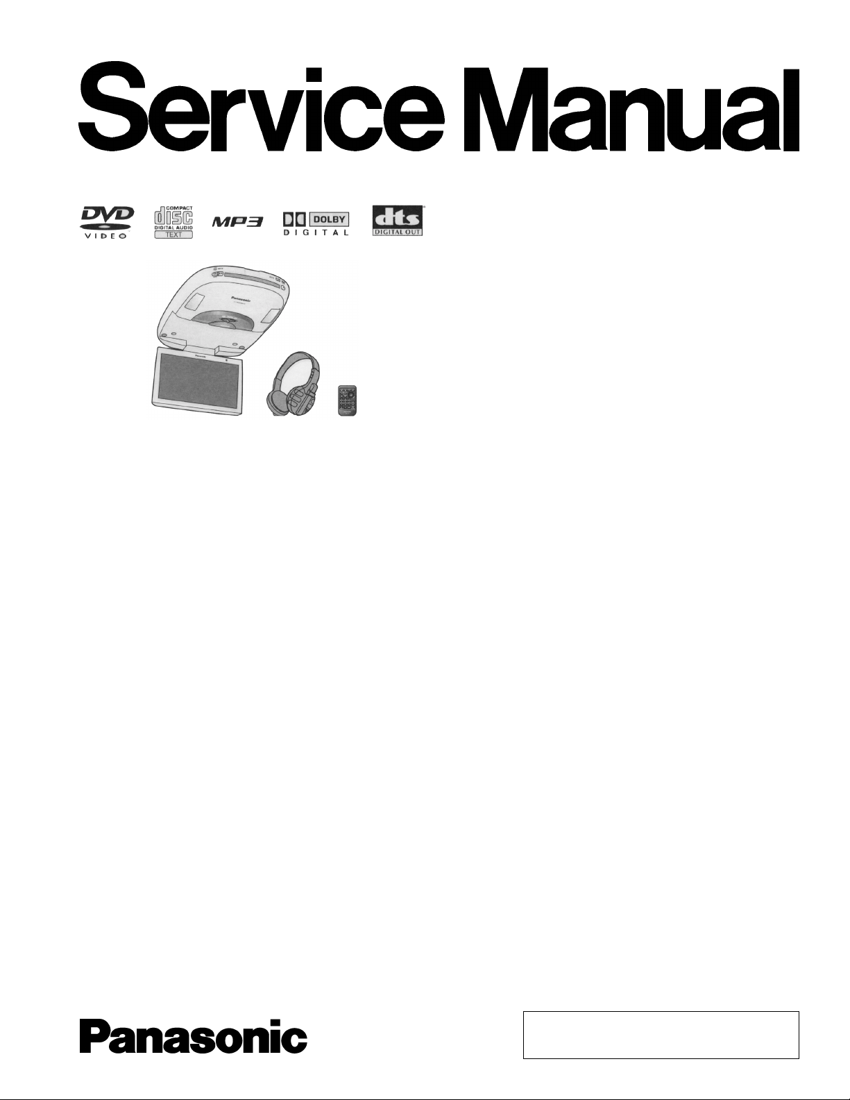
Panasonic CYVHD-9401-N Service manual
ORDER NO.ACED050205C8
AUTOMOTIVE AFTERMARKET
CY-VHD9401N
Overhead 9” Widescreen Color LCD
Monitor with Built-in DVD Player
Specifications*
Overall System
General
Power Supply DC 12V (11V-16V),
Test Voltage 14.4V
Negative Ground
Current Consumption Less than 2.0A
(Without Dome Light)
Usage Temperature Range 10°C to 40°C
Storage Temperature Range -20°C to 80°C
Bulbs for Dome Light DC12V, 5W 2 Pieces
Video Input Signal Composite Video Signal
1.0Vp-p (75Ω)
Video Output Signal Composite Video Signal
1.0Vp-p (75Ω)
Video section
Signal Format PAL/NTSC
Video Output 75Ω, 1 Vp-p
Region Number 2 and ALL
Laser products
Wave length 650 nm
Laser power No hazardous radiation is emitted with
safety protection
Disc Played
(1) DVD Video Disc 12cm Single-sided,
single-layer/double layer
12cm Double-sided,
single-layer/double layer
(2) Compact Disc (CD-DA,
Video CD, CD-R, CD-RW)
Audio section
Audio Input Sensitivity 2.0Vrms (VTR1, VTR2)
Pre-amp Output Voltage 1.8Vrms
Pre-amp Output Impedance 600Ω
Output Voltage/ Impedance 1.8Vrms/ 600Ω
Audio Signal Output
Characteristics
(1) Frequency Response 20Hz - 20kHz (CD)
(2) S/N Ratio 95dB (IHF, A)
(3) Wow and Flutter Below Measurable Limits
Digital audio output
Sound recording format Optical digital audio output form
Disc
DVD video
Dolby Digital Dolby Digital bitstream (1-5.1 ch)
DTS*** DTS bitstream (1-5.1 ch)
Linear PCM
(48 kHz 16/20/24 bit)
Video CD
12cm Disc
20Hz - 22kHz
(DVD Video 48kHz Sampling)
20Hz - 44kHz
(DVD Video 96kHz Sampling)
connector
(The analog portion is not output.)
Linear PCM (2 ch)
(48 kHz sampling /16 bit only)
© 2005 Matsushita Electric Industrial Co., Ltd. All
rights reserved. Unauthorized copying and
distribution is a violation of law.
CY-VHD9401N
MPEG 1 MPEG 1 bitstream
Linear PCM Linear PCM (2 ch) (44.1 kHz
sampling/16 bit)
CD
Linear PCM Linear PCM (2 ch) (44.1 kHz
sampling/16 bit)
DTS*** DTS bitstream (1-5.1 ch)
(The analog portion is not output.)
MP3
MP3 Linear PCM (2 ch)
(32 kHz/44.1 kHz sampling/16 bit)
*** DTS only works with optical outputs.
Light Source 3-Wavelength Straight Cold-Cathode
Tube/Edgelight
Dimensions (W×H×D)** 375×250×56mm
Weight** 3.0 kg
IR Wireless Headphones
Type Open-air Dynamic Stereo Headphones
Unit 40mm Diameter
Power Supply DC 3V (Two R03, AAA, UM-4
Batteries)
Display Unit
Liquid Crystal Panel 9” widescreen
Screen Dimensions
Width 198mm
Height 112mm
Diagonal 227mm
Number of Pixels 336 960 Pixels
(234 Vertical×480 Horizontal×3)
Display Method RGB Vertical Stripe
Drive Method a-SiTFT Active Matrix Format
Dimensions (W×H×D)**
Weight** 210g (Including Batteries)
* Specifications and the design are subject to possible modification
without notice due to improvements.
** Dimensions and Weight shown are approximate.
** Above specifications comply with EIA standards.
(When The Unit is Extended
Maximally)
180×205×80mm
CONTENTS
Page Page
3
1 ABOUT LEAD FREE SOLDER (PbF)
2 LASER PRODUCTS
3 FEATURES
4 REPLACING THE FUSE
5 MAINTENANCE
6 NOTES
7 DIMENSIONS
8 WIRING CONNECTION
9 DISASSEMBLY INSTRUCTIONS
10 TERMINAL S DESCRIPTION
11 IC BLOCK DIAGRAM 9
3
12 REPLACEM ENT PARTS LIST
13 EXPLODED VIEW (Unit)
3
3
14 DVD PLAYER PARTS LIST
3
15 EXPLODED VIEW [DVD Deck]
16 WIRING DIAGRAM
3
3
17 SCHEMAT IC DIAGRAM -1
4
18 SCHEMAT IC DIAGRAM -2
19 BLOCK DIAGRAM
5
6
2
15
25
27
31
32
39
41
47

CY-VHD9401N
1 ABOUT LEAD FREE
SOLDER (PbF)
Distinction of PbF PCB:
PCBs (manufactured) using lead free solder will have a PbF
stamp on the PCB.
Caution :
•
•
Pb free solder has a higher melting point than standard
• •
solder; Typically the melting point is 50 - 70°F (30 40°C) higher. Please use a soldering iron with
temperature control and adjust it to 700 ± 20°F (370 ±
10°C). In case of using high temperature soldering iron,
please be careful not to heat too long.
•
•
Pb free solder will tend to splash when heated too high
• •
(about 1100°F/600°C)
•
•
This lead free solder will be used for the products after
• •
serial No. 1,000,001.
2 LASER PRODUCTS
3 FEATURES
•
•
9 inch Flip-down Overhead Monitor
• •
•
•
Built-in DVD Video Player
• •
•
•
Built-in IR Transmitter for Wireless Headphones
• •
•
•
Game Position
• •
•
•
2 sets of VTR Input Terminals (PAL/NTSC) and 1 set each
• •
of VTR Output and Video Output Terminals (PAL)
•
•
Digital Audio Output Terminal for Upgrading to Dolby Digital
• •
and dts Surround
•
•
Monitor Position and Angle Adjustment Functions
• •
4 REPLACING THE FUSE
Use fuses of the same specified rating 3 amps. Using different
substitutes or fuses with higher ratings, or connecting the unit
directly without a fuse, could cause fire or damage to the stereo
unit.
5 MAINTENANCE
Your products is designed and manufactured to ensure a
minimum of maintenance. Use a soft cloth for routine exterior
cleaning. Never use benzine, thinner or other solvent.
6 NOTES
[DVD DECK BLOCK]
This model has no servo alignment points because
microcomputer controls the servo circuit
7 DIMENSIONS
3
CY-VHD9401N
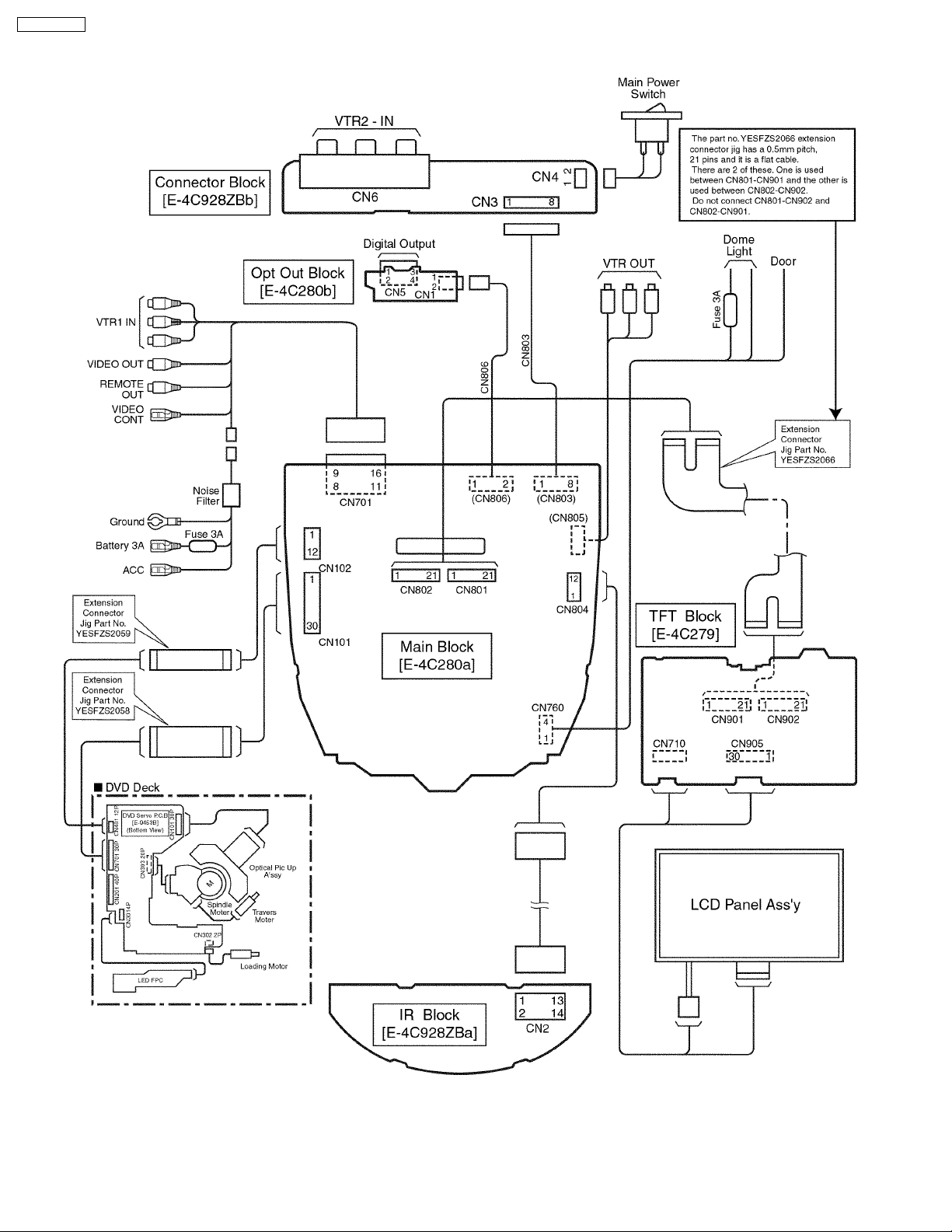
8 WIRING CONNECTION
4
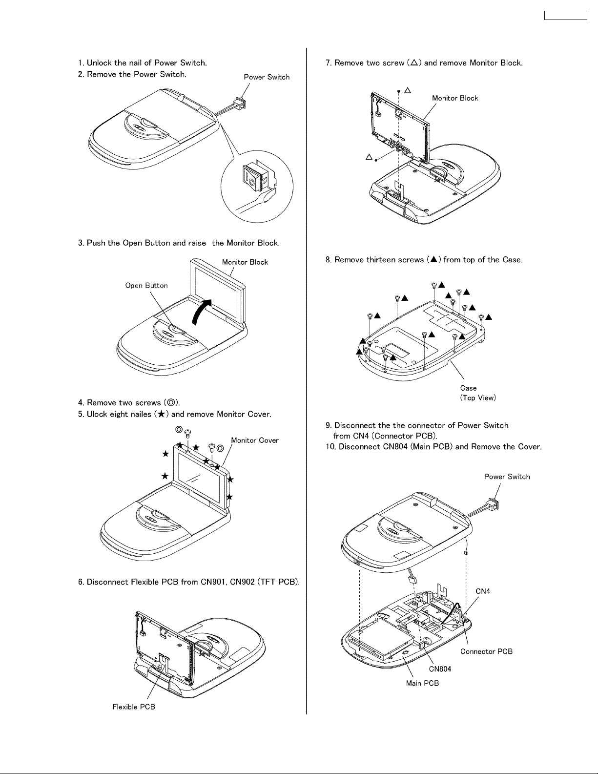
9 DISASSEMBLY INSTRUCTIONS
CY-VHD9401N
5
CY-VHD9401N
10 TERMINALS DESCRIPT ION
10.1. Main Block
IC601 : C2DBJH000034
Pin
No.
1 SD SI SD Card data O 0
2 SD CLK SD Card clock O 0
3 OSDC CS OSD controller chip select O 3.6
4 OSDC COM OSD controller COM O 0.8
5 OSDC SCK OSD controller SCK O 1.5
6 EVDD Power supply (+5V) - 5.2
7 EVSS Ground - 0
8 OSDC REST OSD controller Reset O 5.1
9 BEEP Buzzer output O 0
10 REMO DATA Remote control data I 0
11 NC (Connecting to ground) - 0
12 VD COUNT VD Control O 0
13 DVD MUTE DVD mute O 0
14 NC (Connecting to ground) - 0
15 NC (Connecting to ground) - 0
16 DVD RESET DVD reset O 0
17 DVD CNT DVD power control O 5.2
18 IC/VPP - - 0
19 IR CNT IR modulator output control O 5.2
20 NC (Connecting to ground) - 0
21 NC (Connecting to ground) - 0
22 NC (Connecting to ground) - 0
23 NC (Connecting to ground) - 0
24 NC (Connecting to ground) - 0
25 EJECT LED Eject LED control O 5.2
26 LED CONT
27 EJECT Eject switch signal I 5.2
28 NC (Connecting to ground) - 29 NC (Connecting to ground) - 30 NC (Connecting to ground) - 31 RESET Reset I 5.2
32 XT1 (Connecting to ground) - 0
33 XT2 (NC) No Connection - 34 CPUREG (Capacitor for internal
35 X2 Crystal oscillator - 1.6
36 X1 Crystal oscillator - 1.5
37 VSS Ground - 0
38 VDD Power supply (+5V) - 5.2
39 CLKOUT(NC) No Connection - 40 NC (Connecting to ground) - 0
41 NC (Connecting to ground) - 0
42 NC (Connecting to ground) - 0
43 NC (Connecting to ground) - 0
44 NC (Connecting to ground) - 0
45 NC (Connecting to ground) - 0
46 SYS PWR System powe control O 5.1
47 MAIN PWR Main power control O 5.2
48 MONI CNT Monitor power control O 5.1
49 VIDEO CNT Video control signal I 5.4
50 CLOSE SW Close Switch signal I 0
51 CTL1 - O 0
52 NC (Connecting to ground) - 0
53 CTL2 - O 0
54 NC (Connecting to ground) - 0
55 BVDD Power supply (+5V) 5.2
56 BVSS Ground - 0
57 NC (Connecting to ground) - 0
58 NC (Connecting to ground) - 0
59 NC (Connecting to ground) - 0
Port Description I/O (V)
No Connection - -
(NC)
- 3.3
regulation)
Pin
No.
60 NC (Connecting to ground) - 0
61 NC (Connecting to ground) - 0
62 SD 3.2 Not Used O 0
63 SD 5.5 Not Used O 5.2
64 SD MUTE EN Not Used O 0
65 SD V MUTE Not Used O 5.2
66 SYS MUTE System mute O 0
67 NC (Connecting to ground) - 0
68 NC (Connecting to ground) - 0
69 NC (Connecting to ground) - 0
70 NC (Connecting to ground) - 0
71 AVDD Power supply (+5V) - 5.2
72 AVSS Ground - 0
73 AVREF Analog reference voltage - 5.4
74 A/D KEY Key switch analog input I 5.4
75 LIGHT SENS Dimmer sensor signal I 0.6
76 NC (Connecting to ground) - 0
77 NC (Connecting to ground) - 0
78 NC (Connecting to ground) - 0
79 NC (Connecting to ground) - 0
80 NC (Connecting to ground) - 0
81 NC (Connecting to ground) - 0
82 NC (Connecting to ground) - 0
83 NC (Connecting to ground) - 0
84 NC (Connecting to ground) - 0
85 NC (Connecting to ground) - 0
86 NC (Connecting to ground) - 0
87 NC (Connecting to ground) - 0
88 BATT SENS BATT voltage detection signal I 5.2
89 ACC SENS ACC voltage detection signal I 5.2
90 NC (Connecting to ground) - 0
91 NC (Connecting to ground) - 0
92 AV MUTE AV mute signal (for AV
93 NC (Connecting to ground) - 0
94 I2C SDA I2C sirial data O 5.4
95 NC (Connecting to ground) - 0
96 I2C SCL I2C clock O 5.2
97 DVD DO DVD data I 4.8
98 DVD DI DVD data O 5.1
99 NC (Connecting to ground) - 0
100 SD SO Not Used I 0
Port Description I/O (V)
O 0
switch)
6
10.2. DVD Servo Block
IC501 C1AB00001622
Pin
No.
1 VDDIO I/O pad power (3.3V) - 3.3
2 MD10 SDRAM data bus I/O 0
3 MD11 SDRAM data bus I/O 0.6
4 VDD Core power (1.8V) - 1.8
5 MD12 SDRAM data bus I/O 0
6 VSSIO I/O pad ground - 0
7 MD13 SDRAM data bus I/O 0.7
8 MD14 SDRAM data bus I/O 0.5
9 MD15 SDRAM data bus I/O 0
10 VDDIO I/O pad power (3.3V) - 3.3
11 /DQM1 SDRAM data byte enable O 0
12 MA9 SDRAM address bus O 0
13 MA8 SDRAM address bus O 0
14 VSSIO I/O pad ground - 0
15 MA7 SDRAM address bus O 2.3
16 MA6 SDRAM address bus O 1.9
17 VSS Core ground - 0
18 MA5 SDRAM address bus O 1.1
19 VDDIO I/O pad power (3.3V) - 3.3
20 MA4 SDRAM address bus O 2.0
21 MA3 SDRAM address bus O 2.3
22 MCLK SDRAM clock O 1.7
23 VSSIO I/O pad ground - 0
24 CKE SDRAM clock enable O 3.3
25 MA2 SDRAM address bus O 2.3
26 MA1 SDRAM address bus O 1.0
27 VDDIO I/O pad power (3.3V) - 3.3
28 MA0 SDRAM address bus O 1.0
29 MA10 SDRAM address bus O 0
30 MA11 Not used - 31 VSSIO I/O pad ground - 0
32 MA12 SDRAM address bus O 2.1
33 MA13 SDRAM address bus O 2.1
34 VDD Core power (1.8V) - 1.8
35 /CS0 SDRAM primary bank chip select O 2.7
36 VDDIO I/O pad power (3.3V) - 3.3
37 /RAS SDRAM command bit O 3.1
38 /CAS SDRAM command bit O 2.9
39 /WE SDRAM command bit O 3.2
40 VSSIO I/O pad ground - 0
41 /DQM0 SDRAM data byte enable O 0
42 /DQM2 SDRAM data byte enable O 0
43 MD16 SDRAM data bus I/O 0.5
44 VDDIO I/O pad power (3.3V) - 3.3
45 MD17 SDRAM data bus I/O 0.5
46 MD18 SDRAM data bus I/O 0.5
47 VSS Core ground - 0
48 MD19 SDRAM data bus I/O 0.7
49 VSSIO I/O pad ground - 0
50 MD20 SDRAM data bus I/O 0
51 MD21 SDRAM data bus I/O 1.5
52 MD22 SDRAM data bus I/O 1.0
53 VDDIO I/O pad power (3.3V) - 3.3
54 MD23 SDRAM data bus I/O 0
55 MD24 SDRAM data bus I/O 0.5
56 MD25 SDRAM data bus I/O 0.5
57 VSSIO I/O pad ground - 0
58 MD26 SDRAM data bus I/O 0.5
59 MD27 SDRAM data bus I/O 0.8
60 MD28 SDRAM data bus I/O 0
61 MD29 SDRAM data bus I/O 1.0
62 VDDIO I/O pad power (3.3V) - 3.3
63 MD30 SDRAM data bus I/O 0.7
64 MD31 SDRAM data bus I/O 0.5
65 /DQM3 SDRAM data byte enable O 0
66 /CS1 Not used - 67 VSSIO I/O pad ground - 0
68 SPDIF S/PDIF digital audio output O 1.3
69 VSS Core ground - 0
Port Descriptions I/O(V)Vol
(V)
CY-VHD9401N
Pin
No.
70 AIN Digital audio input for digital micro I 3.3
71 AOUT3 Serial audio data (Left/Right CH) O 0
72 AOUT2 Serial audio data (Center/LFE CH) O 0
73 AOUT1 Serial audio data (Sound Left/Right CH) O 0
74 AOUT0 Serial audio data (Left/Right CH) O 0
75 VDDIO I/O pad power (3.3V) - 3.3
76 PCMCLK Audio DAC PCM sampling clock O 1.8
77 VDD Core power (1.8V) - 1.8
78 ACLK Audio interface serial data clock O 1.7
79 LRCLK Left/Right channel clock O 1.7
80 /SRST Reset signal O 3.3
81 /RSTP Power on reset I 3.3
82 VSSIO I/O pad ground - 0
83 RXD1 Not used - 84 SSPIN1 SSP1 data in / UART1 16X clock I/O 15
85 VSS Core ground - 0
86 SSPOUT1 SSP1 sata out / UART1 DTR I/O 0
87 SSPCLK1 SSP1 clock / UART1 CTS I/O 3.3
88 SSPCLK0 Not used - 89 VDD Core power (1.8V) - 1.8
90 SSIN0 Not used - 91 VDDIO I/O pad power (3.3V) - 3.3
92 SSPOUT0 Not used - 93 TXD0 UART0 serial data O 3.2
94 RXD0 UART0 serial data I 3.0
95 /CTS0 Not used - 96 /RTS0 Not used - 97 VSSIO I/O pad ground - 0
98 CXI Crystal Oscillator terminal I 1.6
99 CXO Not used - 100 OSCVSS Oscillator ground - 0
101 OSCVDD Oscillator power (1.8V) - 1.8
102 MVCLVDD Main/Video clock PLL power (3.3V) - 3.3
103 SCEN Not used - 104 MVCKVSS Main/Video clock PLL Ground - 0
105 ACLKVSS Audio clock PLL ground - 0
106 SCMD Not used - 107 ACLKVDD Audio clock PLL power - 3.3
108 VDDDAC DAC digital power (1.8V) - 1.8
109 VSSDAC DAC digital ground - 0
110 CVBS2/CR/R Composite Cr/Component Cr/SCART Red O 0.5
111 IOM Cascaded DAC differential output O 1.0
112 C/CB/B Chrominance/Component Cb/SCART Cb O 0.7
113 VAA3 DAC analog power (3.3V) - 3.3
114 Y/G Luminance/SCART G O 0.4
115 VSSA DAC analog ground - 0
116 VREF Not used - 117 VAA - - 1.8
118 CVBS/C Composite/S-Video Chrominance O 0.5
119 RSET Current setting resistor connection O 1.4
120 COMP Compensation capacitor connection O 2.0
121 VSS Core ground - 0
122 VCLK Not used - 123 VSYNC Not used - 124 HSYNC Not used - 125 VDDIO I/O pad power (3.3V) - 3.4
126-
131
132 VSSIO I/O pad ground - 0
133 Not used - 134 Not used - 135 VDD Core power (1.8V) - 1.9
136-
139
140 VDDIO I/O pad power (3.3V) - 3.4
141-
144
145 /PWE3 Not used - 146 AD23 Not used - 147 VSSIO I/O pad ground - 0
148-
150
151-
153
Port Descriptions I/O(V)Vol
VI07-02 Not used - -
AD31-28 Not used - -
AD27-24 Not used - -
AD22-20 Not used - -
AD19-17 Address/Data bus I/O 0
(V)
7
CY-VHD9401N
Pin
No.
154 VDDIO I/O pad power (3.3V) - 3.4
155 AD16 Address/Data bus I/O 0
156 /PWE2 Not used - -
157,
158
159 VDD Core power (1.8V) - 1.9
160 SCLK External bus clock O 2.1
161 ACK Programmable WAIT/ACK/RDY control I 3.4
162 VSSIO I/O pad ground - 0
163-
168
169 VDDIO I/O pad power (3.3V) - 3.4
170 /PWE1 Not used - 171 VSS Core ground - 0
172-
176
177 VSSIO I/O pad ground - 0
178-
180
181 VDDIO I/O pad power (3.3V) - 3.4
182 /PWE0 Byte write enable O 0
183 ALE Address latch enable O 0
184-
187
188 VSSIO I/O pad ground - 0
189 RD Read signal O 3.4
190 LHLDA Not used - 191 LHLD Not used - 192 VDD Core power (1.8V) - 1.9
193 /PCS0 Peripheral chip select 0 O 3.4
194 XI01 Not used - 195 DACCS2 DAC output select 2 O 3.4
196 VDDIO I/O pad power (3.3V) - 3.4
197 DACCS1 DAC output select 1 O 3.4
198 NINTCPPM Not used - 199 CPPMCS Not used - 200 XI06 Not used - 201 VSS Core ground - 0
202 FRAMCS FRAM chip selection O 0
203 DACRST DAC reset O 0
204 VSSIO I/O pad ground - 0
205 FEPCS Front End Pro. LSI chip select O 3.4
206 FEPRST Front End Pro. reset O 3.4
207 SODCCS SODC LSI chip selection O 3.4
208 NINTHOST HOST interrupt I 3.4
209 NINTDDC DDC interrupt I 3.2
210 VDDIO I/O pad power (3.3V) - 3.4
211 NINTDSC DSC interrupt I 3.5
212 VDD Core power (1.8V) - 1.9
213 DSYNV DVD parallel mode sector SYNC I 3.4
214 DREQ DVD parallel mode data request O 3.4
215 DCLK Data sampling clock I 3.4
216 DSTB Parallel mode data valid/Serial mode clock I 0.7
217 DVD0 DVD drive parallel data port I 0
218 VSSIO I/O pad ground - 0
219 DVD1 DVD drive parallel data port I 0
220 DVD2 DVD drive parallel data port I 0
221 DVD3 DVD drive parallel data port I 3.4
222 DVD4 DVD drive parallel data port I 0.8
223 DVD5 DVD drive parallel data port I 0.8
224 VDDIO I/O pad power (3.3V) - 3.4
225 DVD6 DVD drive parallel data port I 3.4
226 DVD7 DVD drive parallel data port I 3.4
227 MD0 SDRAM data bus I/O 0.5
228 VSSIO I/O pad ground - 0
229 MD1 SDRAM data bus I/O 0
230 VSS Core ground - 0
231 MD2 SDRAM data bus I/O 0.8
232 MD3 SDRAM data bus I/O 0.8
233 VDDIO I/O pad power (3.3V) - 3.3
234 MD4 SDRAM data bus I/O 3.3
235 MD5 SDRAM data bus I/O 0
236 MD6 SDRAM data bus I/O 0.8
237 VSSIO I/O pad ground - 0
Port Descriptions I/O(V)Vol
AD15, 14 Address/Data bus I/O 0
AD13-08 Address/Data bus I/O 0
AD7-3 Address/Data bus I/O 0
AD02-00 Address/Data bus I/O 0
LA0-3 Latch address O 3.3
(V)
Pin
No.
238 MD7 SDRAM data bus I/O 0
239 MD8 SDRAM data bus I/O 0
240 MD9 SDRAM data bus I/O 0
Port Descriptions I/O(V)Vol
(V)
8
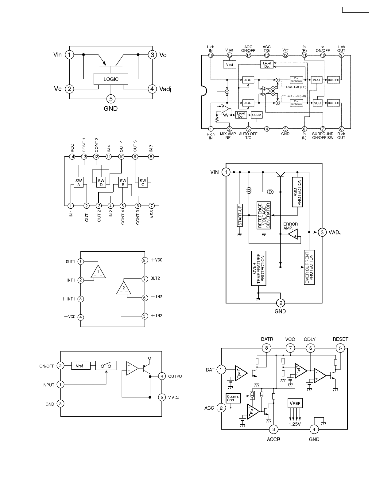
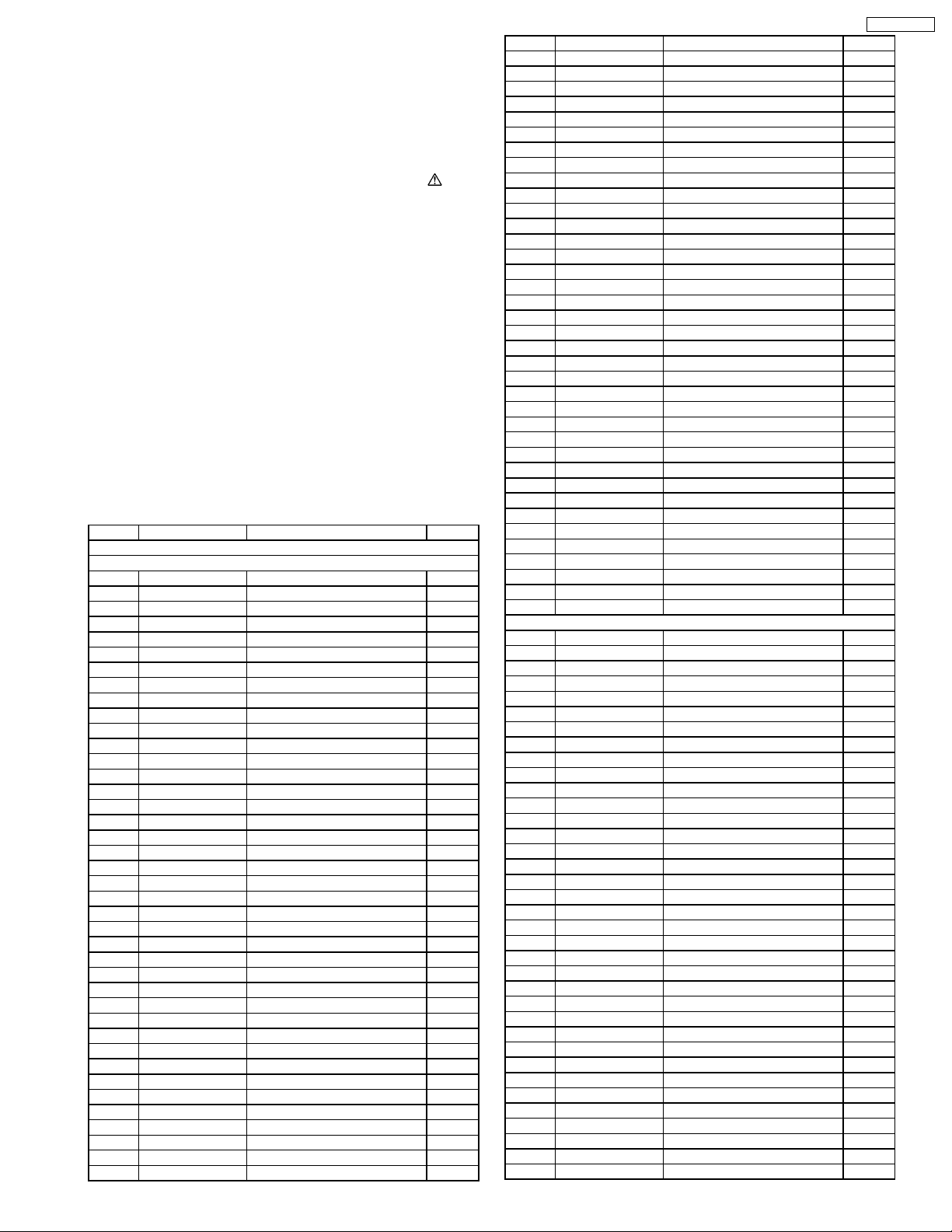
11 IC BLOCK DIAGRAM
11.1. Main Block
IC120 : C0DBEZG00010
CY-VHD9401N
IC371 : C1BB00000710
IC261 : C0JBZS000003
IC370 : C0ABBB000179
IC701 : C0CBYA00006
IC730 : C0DBEKG00001
IC702 : AN8065SE1
9
CY-VHD9401N
11.2. IR Block
IC850: C0DBAMA00005
IC640 : PNA4602M01MC
10
11.3. TFT Block
CY-VHD9401N
IC801 : AN2526FH
IC802 : C1AB00000279
11
CY-VHD9401N
IC805 : C0ZBZ0000432
IC806 : C3EBCC000033
IC905 : C0FBBD000038
12
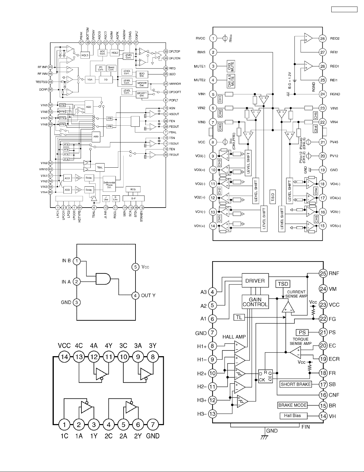
11.4. DVD Deck Block
CY-VHD9401N
IC101 : AN8703FH-V
IC271 : YEAMT7ST08UL
IC311 : C0GBY0000012
IC275, IC561 : C0JBAZ001014
IC321 : C0GBH0000006
13
CY-VHD9401N
IC411 : YEAMC78L05E2
IC441 : MN13821JP
IC651 : C3GBCC000001
IC652 : C0JBAB000255
IC631, IC641 : C0JBAH000082
14
12 REPLACEMENT PARTS
LIST
Notes :
1. Be sure to make your orders of replacement parts
according to this list.
2. Important safety notice: Components, identified by
have special characteristics important for safety. When
replacing any of these components, use only
manufacturer´s specified parts.
3. Location keys in the remarks column indicates the general
location of the parts shown in the exploded drawing, as in a
road map.
4. The marking (RTL) indicates that Retention Time is limited
for this item. After the discontinuation of assembly in
production, the item will continue to be available for a
specific period of time. The retention period of availability is
dependent on the type of assembly, and in accordance with
the laws governing part and product retention. After the end
of this period, the assembly will no longer be available.
•
•
Order intake period is basically six months after the first
• •
shipment.
5. “T” marks in remarks colum are indicated supply parts of
TAMACO.
Ref. No. Part No. Part Name & Description Remarks
[E-4C280a/b] Main/ Opt Out Block
IC´s and TRANSISTORs
IC10 YEAMPJ78L05AC IC T
IC120 C0DBEZG00010 IC
IC121 C0ABBB000090 IC
IC130 C0JBAA000115 IC
IC140 C0JBAA000102 IC
IC150 C0JBAA000115 IC
IC211 C0ABBB000090 IC
IC261 C0JBZS000003 IC
IC330 C0ABBB000090 IC
IC340 C0ABBB000090 IC
IC370 C0ABBB000179 IC
IC371 C1BB00000710 IC T
IC401 C1AB00000284 IC
IC402 C1AB00001604 IC
IC601 C2DBJH000034 IC T
IC602 C0JBAA000115 IC
IC631 C0JBAZ000525 IC
IC701 C0CBAYA00006 IC
IC702 AN8065SE1 IC
IC720 C0ABAB000001 IC
IC730 C0DBEKG00001 IC
IC801 YEAM5001IDR IC
IC850 C0DBAMA00005 IC
Q10 YEANFP1F3PT1 Transistor
Q11 B1GBCFNN0004 Transistor
Q130 B1GBCFJJ0002 Transistor
Q131 B1GBCFJJ0002 Transistor
Q250 XN0F26100L Transistor
Q251 B1GBCFNN0004 Transistor
Q270 YEANDTC323TK Transistor
Q351 B1GBCFNN0004 Transistor
Q362 2SD0601AHR Transistor
Q370 YEANDTC323TK Transistor
Q400 2SD11190LL Transistor
Q401 YEANA812T2 Transistor
Q430 2SD11190LL Transistor
Q431 YEANA812T2 Transistor
Q450 2SB0709AWL Transistor
Q460 2SB0709AWL Transistor
Q470 2SB0709AWL Transistor
mark
CY-VHD9401N
Ref. No. Part No. Part Name & Description Remarks
Q631 B1GBCFJN0009 Transistor
Q640 B1GBCFNN0004 Transistor
Q656 B1GBCFNN0004 Transistor
Q680 YEANA124EKTX Transistor
Q681 B1GDCFJJ0002 Transistor
Q682 B1GBCFNN0004 Transistor
Q701 B1BDEL000001 Transistor
Q702 YEANFB1F3PT1 Transistor
Q703 2SB10730LL Transistor
Q704 YEANC3618 Transistor
Q705 B1GBNCEJ0001 Transistor
Q706 B1GBCFJJ0002 Transistor
Q707 B1BBCG000002 Transistor
Q719 B1DFDG000006 Transistor
Q720 B1BBCG000002 Transistor
Q721 2SB1572T1 Transistor T
Q760 YEANFP1F3PT1 Transistor
Q761 B1DFDG000006 Transistor
Q762 YEANFB1F3PT1 Transistor
Q770 YEANC114YKX Transistor
Q801 2SB0709AWL Transistor
Q802 B1GBCFJN0009 Transistor
Q803 2SD0601AHR Transistor
Q804 B1DHGD000005 Transistor
Q805 B1BDEL000001 Transistor
Q806 YEANFB1F3PT1 Transistor
Q807 2SB0709AWL Transistor
Q850 B1GDCFJJ0002 Transistor
Q851 B1BDEL000001 Transistor
Q852 2SD0601AHR Transistor
Q853 YEANFP1F3PT1 Transistor
Q854 B1GBCFJJ0002 Transistor
Q855 B1GDCFJJ0002 Transistor
Q856 2SD0601AHR Transistor
Q857 B1BDEL000001 Transistor
DIODEs
D250 YEADAP202KTX Diode
D251 MA3X15300L Diode
D280 MA2J72900L Diode
D362 MA3X152A0L Diode
D370 B0ADCJ000025 Diode
D380 MA2J72900L Diode
D601 MA2J72900L Diode
D630 MA3X152E0L Diode
D631 B0BC5R600010 Diode T
D650 B0BC5R600010 Diode T
D651 YEAD1921BHC LED T
D652 YEAD1921BHC LED T
D653 YEAD1921BHC LED T
D680 YEADAP202KTX Diode
D701 B0BA04700003 Diode
D702 B0JCRC000002 Diode
D703 B0ACCK000005 Diode
D704 B0ECKL000001 Diode
D705 YEADSR1544TL Diode
D706 B0ACCK000005 Diode
D707 B0BC5R600004 Diode
D708 YEADRD91M2T2 Diode T
D709 YEADDAN202KT Diode
D720 B0JCRC000002 Diode
D760 B0BA04700003 Diode
D761 YEADRD51MBT1 Diode
D762 YEADDAN202KT Diode
D763 YEADDAN202KT Diode
D764 YEADDAN202KT Diode
D765 B0BC5R600004 Diode
D801 B0JCQD000002 Diode
D850 B0JCQD000002 Diode
D851 B0ADCJ000012 Diode
D852 B0ADCJ000012 Diode
D853 B0JCQD000002 Diode
15
CY-VHD9401N
Ref. No. Part No. Part Name & Description Remarks
CAPACITORs
C10 F1J1C334A006 Ceramic, 0.33µF 16WV
C11 F1J1C334A006 Ceramic, 0.33µF 16WV
C12 ECEV1CA100SR Electrolytic, 10µF 16WV
C13 F1H1H104A842 Chip, 0.1µF 50WV T
C14 ECEV0JA221WP Electrolytic, 220µF 6.3WV
C15 F1H1H104A842 Chip, 0.1µF 50WV T
C16 ECEV1CA101P Electrolytic, 100µF 16WV
C80 F1J1C104A148 Chip, 0.1µF 16WV T
C81 F1J1C104A148 Chip, 0.1µF 16WV T
C82 F1J1C104A148 Chip, 0.1µF 16WV T
C83 F1J1C104A148 Chip, 0.1µF 16WV T
C84 F1J1C104A148 Chip, 0.1µF 16WV T
C85 F1J1C104A148 Chip, 0.1µF 16WV T
C86 ECEV1CA100SR Electrolytic, 10µF 16WV
C87 F1J1C104A148 Chip, 0.1µF 16WV T
C88 F1J1C104A148 Chip, 0.1µF 16WV T
C89 F1J1C104A148 Chip, 0.1µF 16WV T
C133 F1H1H104A842 Chip, 0.1µF 50WV T
C134 F3G1C226A001 Tantal, 22µF 16WV
C135 F1H1H104A842 Chip, 0.1µF 50WV T
C136 ECUV0J106KBM Chip, 10µF 6.3WV
C137 ECUV0J106KBM Chip, 10µF 6.3WV
C138 F1H1H104A842 Chip, 0.1µF 50WV T
C139 F1H1H104A842 Chip, 0.1µF 50WV T
C140 F1H1H104A842 Chip, 0.1µF 50WV T
C141 F1K1C225A069 Chip, 2.2µF 16WV T
C142 EEVFC1C100R Electrolytic, 10µF 16WV
C143 F1K1C225A069 Chip, 2.2µF 16WV T
C144 EEVFC0J101P Electrolytic, 100µF 6.3WV
C145 F1K1C225A069 Chip, 2.2µF 16WV T
C146 EEVFC0J101P Electrolytic, 100µF 6.3WV
C147 F1K1C225A069 Chip, 2.2µF 16WV T
C148 EEVFC0J101P Electrolytic, 100µF 6.3WV
C150 F1H1H104A842 Chip, 0.1µF 50WV T
C213 F1J1C105A173 Chip, 1µF 16WV T
C230 ECEV1CA100SR Electrolytic, 10µF 16WV
C231 ECEV1CA100SR Electrolytic, 10µF 16WV
C232 F1H1H331A842 Chip, 330PF 50WV T
C233 F1J1C105A173 Chip, 1µF 16WV T
C234 F1H1H331A842 Chip, 330PF 50WV T
C235 ECEV1CA220SR Electrolytic, 22µF 16WV
C236 F1H1H104A842 Chip, 0.1µF 50WV T
C240 ECEV1CA100SR Electrolytic, 10µF 16WV
C241 ECEV1CA100SR Electrolytic, 10µF 16WV
C242 F1H1H331A842 Chip, 330PF 50WV T
C243 F1J1C105A173 Chip, 1µF 16WV T
C244 F1H1H331A842 Chip, 330PF 50WV T
C245 ECEV1CA220SR Electrolytic, 22µF 16WV
C246 F1H1H104A842 Chip, 0.1µF 50WV T
C251 F1H1H102A842 Chip, 1000PF 50WV T
C252 ECEV1EA4R7SR Electrolytic, 4.7µF 25WV
C253 F1H1H560A841 Chip, 56PF 50WV T
C256 ECEV1AA101SP Electrolytic, 100µF 10WV
C257 ECEV1HA2R2SR Electrolytic, 2.2PF 50WV
C258 F1J1A225A063 Chip, 2.2µF 10WV T
C260 F1L1C4750005 Electrolytic, 4.7µF 16WV
C262 F1H0J1050010 Chip, 1µF 6.3WV
C263 ECUV1H101KBN Chip, 100PF 50WV
C264 ECUV1H101KBN Chip, 100PF 50WV
C265 ECEV1CA100SR Electrolytic, 10PF 16WV
C266 ECEV1CA100SR Electrolytic, 10PF 16WV
C267 ECEV1CA220SR Electrolytic, 22µF 16WV
C268 F1J1H104A036 Chip, 0.1µF 50WV
C269 ECEV1CA100SR Electrolytic, 10µF 16WV
C270 F1J1C105A173 Chip, 1µF 16WV T
C271 F1J1C105A173 Chip, 1µF 16WV T
C272 F1H1H392A842 Chip, 3900PF 50WV T
C273 F1J1C224A173 Chip, 0.22µF 16WV T
C274 F1H1H392A842 Chip, 3900PF 50WV T
C275 ECEV1EA4R7R Electrolytic, 4.7µF 25WV
C276 ECEV1CA220SR Electrolytic, 22µF 16WV
C277 ECEV1CA100SR Electrolytic, 10µF 16WV
Ref. No. Part No. Part Name & Description Remarks
C278 F1H1H104A842 Chip, 0.1µF 50WV T
C279 F1J1C224A173 Chip, 0.22µF 16WV T
C281 F1J1C104A148 Chip, 0.1µF 16WV T
C283 F1H1H104A842 Chip, 0.1µF 50WV T
C313 F1J1C105A173 Chip, 1µF 16WV T
C330 ECEV1CA100SR Electrolytic, 10µF 16WV
C331 ECEV1CA100SR Electrolytic, 10µF 16WV
C332 F1H1H331A842 Chip, 330PF 50WV T
C333 F1J1C105A173 Chip, 1µF 16WV T
C334 ECEV1CA220SR Electrolytic, 22µF 16WV
C335 F1H1H331A842 Chip, 330PF 50WV T
C340 ECEV1CA100SR Electrolytic, 10µF 16WV
C341 ECEV1CA100SR Electrolytic, 10µF 16WV
C342 F1H1H331A842 Chip, 330PF 50WV T
C343 F1J1C105A173 Chip, 1µF 16WV T
C344 ECEV1CA220SR Electrolytic, 22µF 16WV
C345 F1H1H331A842 Chip, 330PF 50WV T
C352 ECEV1EA4R7SR Electrolytic, 4.7µF 25WV
C353 F1H1H560A841 Chip, 56PF 50WV T
C356 F1H1H104A842 Chip, 0.1µF 50WV T
C357 ECEV1HA2R2SR Electrolytic, 2.2PF 50WV
C358 F1J1A225A063 Chip, 2.2µF 10WV T
C362 F1H0J1050010 Chip, 1µF 6.3WV
C363 ECUV1H101KBN Chip, 100PF 50WV
C364 ECUV1H101KBN Chip, 100PF 50WV
C365 ECEV1CA100SR Electrolytic, 10PF 16WV
C366 ECEV1CA100SR Electrolytic, 10PF 16WV
C367 ECEV1CA220SR Electrolytic, 22µF 16WV
C370 F1J1C105A173 Chip, 1µF 16WV T
C371 F1J1C105A173 Chip, 1µF 16WV T
C372 F1H1H392A842 Chip, 3900PF 50WV T
C373 F1J1C224A173 Chip, 0.22µF 16WV T
C374 F1H1H392A842 Chip, 3900PF 50WV T
C375 ECEV1CA470SP Electrolytic, 47µF 16WV
C376 ECEV1CA470SP Electrolytic, 47µF 16WV
C377 F1H1H104A842 Chip, 0.1µF 50WV T
C378 ECEV1CA470SP Electrolytic, 47PF 16WV
C379 F1J1C224A173 Chip, 0.22µF 16WV T
C381 F1J1C104A148 Chip, 0.1µF 16WV T
C401 ECEV1AA101SP Electrolytic, 100µF 10WV
C402 F1H1H104A842 Chip, 0.1µF 50WV T
C403 F1H1H104A842 Chip, 0.1µF 50WV T
C413 F1J1C105A173 Chip, 1µF 16WV T
C430 ECEV1HA010SR Electrolytic, 1µF 50WV
C440 ECEV1HA010SR Electrolytic, 1µF 50WV
C451 ECEV1CA471P Electrolytic, 470µF 16WV
C452 ECEV1AA470WR Electrolytic, 47µF 10WV T
C460 ECEV1AA470WR Electrolytic, 47µF 10WV T
C470 ECEV1AA470WR Electrolytic, 47µF 10WV T
C471 ECEV1CA471P Electrolytic, 470µF 16WV
C472 F1H1H104A842 Chip, 0.1µF 50WV T
C473 F1J1C105A173 Chip, 1µF 16WV T
C601 ECEV0JA101SP Electrolytic, 100µF 6.3WV
C602 F1H1H104A842 Chip, 0.1µF 50WV T
C604 F1H1H104A842 Chip, 0.1µF 50WV T
C605 F1H0J1050010 Chip, 1µF 6.3WV
C606 F1H1H150A841 Chip, 15PF 50WV T
C607 F1H1H150A841 Chip, 15PF 50WV T
C608 ECEV0JA101SP Electrolytic, 100µF 6.3WV
C609 F1H1H104A842 Chip, 0.1µF 50WV T
C610 F1H1H104A842 Chip, 0.1µF 50WV T
C611 ECEV0JA101SP Electrolytic, 100µF 6.3WV
C612 F1K1C105A026 Ceramic, 1µF 16WV
C613 F1K1C105A026 Ceramic, 1µF 16WV
C614 F4D551040007 Electrolytic, 0.1µF 5.5WV
C615 F1H1H104A842 Chip, 0.1µF 50WV T
C631 F1H1H104A842 Chip, 0.1µF 50WV T
C632 F1H1H330A841 Chip, 33PF 50WV T
C650 F1H1H102A842 Chip, 1000PF 50WV T
C680 ECEV1CA100SR Electrolytic, 10µF 16WV
C700 F1H1H104A842 Chip, 0.1µF 50WV T
C701 F2A1C222A715 Electrolytic, 2200µF 16WV T
C702 F1L1C1060016 Ceramic, 10µF 16WV
C703 F1H1H102A842 Chip, 1000PF 50WV T
16
Ref. No. Part No. Part Name & Description Remarks
C704 F1L1C1060016 Ceramic, 10µF 16WV
C705 ECEV1CA101P Electrolytic, 100µF 16WV
C706 F1H1H104A842 Chip, 0.1µF 50WV T
C707 ECEV1CA101P Electrolytic, 100µF 16WV
C708 ECEV1CA100SR Electrolytic, 10µF 16WV
C709 F1H1H104A842 Chip, 0.1µF 50WV T
C710 F1H1H104A842 Chip, 0.1µF 50WV T
C711 F1J1C224A173 Chip, 0.22µF 16WV
C712 F1J1C474A173 Chip, 0.47µF 16WV T
C713 ECEV0JA101SP Electrolytic, 100µF 6.3WV
C714 F1K1C225A069 Chip, 2.2µF 16WV T
C715 EEVFC1C681P Electrolytic, 680µF 16WV
C716 ECEV1CA471P Electrolytic, 470µF 16WV
C717 ECEV1CA101P Electrolytic, 100µF 16WV
C718 F1H1H104A842 Chip, 0.1µF 50WV T
C719 ECEV1AA221P Electrolytic, 220µF 10WV
C723 F1L1C1060016 Ceramic, 10µF 16WV
C724 F1H1H102A842 Chip, 1000PF 50WV T
C725 F1L1C1060016 Ceramic, 10µF 16WV
C726 F1H1H104A842 Chip, 0.1µF 50WV T
C730 ECEV1CA101P Electrolytic, 100µF 16WV
C731 F3G1V1050001 Electrolytic, 1µF 35WV
C732 F1H1H104A842 Chip, 0.1µF 50WV T
C733 F1H1H104A842 Chip, 0.1µF 50WV T
C734 ECEV1CA101P Electrolytic, 100µF 16WV
C760 EEVFC1C681P Electrolytic, 680µF 16WV
C761 F1H1H104A842 Chip, 0.1µF 50WV T
C762 F1J1H104A036 Chip, 0.1µF 50WV
C770 F1H1H104A842 Chip, 0.1µF 50WV T
C801 F2A1C222A715 Electrolytic, 2200µF 16WV T
C802 F1K1C105A026 Ceramic, 1µF 16WV
C803 ECEV1CA221P Electrolytic, 220µF 16WV
C804 F1H1H471A190 Ceramic, 470PF 50WV
C805 F1H1E273A086 Chip, 0.027µF 25WV T
C806 ECUV1C106KBM2 Chip, 10µF 16WV T
C807 F1H1H104A842 Chip, 0.1µF 50WV T
C808 F1H1H104A842 Chip, 0.1µF 50WV T
C809 EEVFC1C331P Electrolytic, 330µF 16WV
C810 F1H1H103A842 Chip, 0.01µF 50WV T
C824 F1H1H103A842 Chip, 0.01µF 50WV T
C850 EEVFC1C681P Electrolytic, 680µF 16WV
C851 EEVFC1C681P Electrolytic, 680µF 16WV
C852 F1J1C104A148 Chip, 0.1µF 16WV T
C853 EEVFC1C681P Electrolytic, 680µF 16WV
C854 F1L1C4750005 Electrolytic, 4.7µF 16WV
C856 F1H1H102A842 Chip, 1000PF 50WV T
C857 EEVFC1C681P Electrolytic, 680µF 16WV
C858 F1K1C225A069 Chip, 2.2µF 16WV T
C859 F1J1C474A173 Chip, 0.47µF 16WV T
C861 F1L1C4750005 Electrolytic, 4.7µF 16WV
C862 F1J1C104A148 Chip, 0.1µF 16WV T
C863 F1H1H102A190 Ceramic, 1000PF 50WV
C864 F1L1C1060016 Ceramic, 10µF 16WV
C865 F1H1H102A842 Chip, 1000PF 50WV T
C866 F1J1C104A148 Chip, 0.1µF 16WV T
C868 F1H1H103A842 Chip, 0.01µF 50WV T
C869 F1J1H151A785 Chip, 150PF 50WV T
C870 F1H1H332A748 Chip, 3300PF 50WV T
C871 F1L1C4750005 Electrolytic, 4.7µF 16WV
C872 EEVFC1C681P Electrolytic, 680µF 16WV
C873 F1J1C104A148 Chip, 0.1µF 16WV T
RESISTORs
R11 D0GDR00JA017 Chip, 0Ω1/8W T
R12 D0GDR00JA017 Chip, 0Ω1/8W T
R13 D0GDR00JA017 Chip, 0Ω1/8W T
R14 D0GDR00JA017 Chip, 0Ω1/8W T
R15 D0GDR00JA017 Chip, 0Ω1/8W T
R16 D0GDR00JA017 Chip, 0Ω1/8W T
R17 D0GDR00JA017 Chip, 0Ω1/8W T
R18 D0GDR00JA017 Chip, 0Ω1/8W T
R20 D1BD4702A030 Chip, 47kΩ1/8W T
R21 D0GD470JA017 Chip, 47Ω1/8W T
CY-VHD9401N
Ref. No. Part No. Part Name & Description Remarks
R22 D0GDR00JA017 Chip, 0Ω1/8W T
R23 D0GDR00JA017 Chip, 0Ω1/8W T
R24 D0GDR00JA017 Chip, 0Ω1/8W T
R26 D0GDR00JA017 Chip, 0Ω1/8W T
R120 D1BD3601A030 Chip, 3.6kΩ1/8W T
R121 D1BD6801A030 Chip, 6.8kΩ1/8W T
R130 D0GB103JA008 Chip, 10kΩ1/10W T
R131 D0GB102JA008 Chip, 1kΩ1/10W T
R132 D0GB103JA008 Chip, 10kΩ1/10W T
R133 D0GB102JA008 Chip, 1kΩ1/10W T
R134 D0GB102JA008 Chip, 1kΩ1/10W T
R150 D0GD101JA017 Chip, 100Ω1/8W T
R151 D0GDR00JA017 Chip, 0Ω1/8W T
R152 D0GD471JA017 Chip, 470Ω1/8W T
R153 D0GDR00JA017 Chip, 0Ω1/8W T
R156 D0GD220JA017 Chip, 22Ω1/8W T
R157 D0GD220JA017 Chip, 22Ω1/8W T
R158 D0GD220JA017 Chip, 22Ω1/8W T
R159 D0GD220JA017 Chip, 22Ω1/8W T
R161 D0GDR00JA017 Chip, 0Ω1/8W T
R163 D0GDR00JA017 Chip, 0Ω1/8W T
R164 D0GFR00JA017 Chip, 0Ω1/8W T
R165 D0GFR00JA017 Chip, 0Ω1/8W T
R166 D0GDR00JA017 Chip, 0Ω1/8W T
R202 D0GB332JA008 Chip, 3.3kΩ1/10W T
R203 D0GB822JA008 Chip, 8.2kΩ1/10W T
R204 D0GB822JA008 Chip, 8.2kΩ1/10W T
R207 D0GB101JA008 Chip, 100Ω1/10W T
R210 D0GDR00JA017 Chip, 0Ω1/8W T
R230 D1BD4702A030 Chip, 47kΩ1/8W T
R231 D0GB183JA008 Chip, 18kΩ1/10W T
R232 D0GB183JA008 Chip, 18kΩ1/10W T
R233 D0GB103JA008 Chip, 10kΩ1/10W T
R234 D0GB103JA008 Chip, 10kΩ1/10W T
R235 D0GB103JA008 Chip, 10kΩ1/10W T
R236 D0GB103JA008 Chip, 10kΩ1/10W T
R240 D1BD4702A030 Chip, 47kΩ1/8W T
R241 D0GB183JA008 Chip, 18kΩ1/10W T
R242 D0GB183JA008 Chip, 18kΩ1/10W T
R243 D0GB103JA008 Chip, 10kΩ1/10W T
R244 D0GB103JA008 Chip, 10kΩ1/10W T
R245 D0GB103JA008 Chip, 10kΩ1/10W T
R246 D0GB103JA008 Chip, 10kΩ1/10W T
R250 D1BD1002A030 Chip, 10kΩ1/8W T
R251 D0GD561JA017 Chip, 560Ω1/8W T
R252 D0GB683JA008 Chip, 68kΩ1/10W T
R253 D0GB363JA008 Chip, 36kΩ1/10W T
R254 D0GB683JA008 Chip, 68kΩ1/10W T
R257 D0GB363JA008 Chip, 36kΩ1/10W T
R259 D0GDR00JA017 Chip, 0Ω1/8W T
R261 D0GB472JA008 Chip, 4.7kΩ1/10W T
R262 D0GB392JA008 Chip, 3.9kΩ1/10W T
R263 D0GB512JA008 Chip, 5.1kΩ1/10W T
R264 D0GD183JA017 Chip, 18kΩ1/8W T
R265 D0GD183JA017 Chip, 18kΩ1/8W T
R266 D0GD363JA017 Chip, 36kΩ1/8W T
R267 D0GD363JA017 Chip, 36kΩ1/8W T
R268 D0GD103JA017 Chip, 10kΩ1/8W T
R270 D0GB822JA008 Chip, 8.2kΩ1/10W T
R271 D0GB822JA008 Chip, 8.2kΩ1/10W T
R272 D0GB153JA008 Chip, 15kΩ1/10W T
R273 D0GB153JA008 Chip, 15kΩ1/10W T
R274 D0GB561JA008 Chip, 560Ω1/10W T
R275 D0GB473JA008 Chip, 47kΩ1/10W T
R276 D0GD103JA017 Chip, 10kΩ1/8W T
R280 D0GBR00JA008 Chip, 0Ω1/10W T
R281 D0GD220JA017 Chip, 22Ω1/8W T
R282 D0GB123JA008 Chip, 12kΩ1/10W T
R283 D0GB272JA008 Chip, 2.7kΩ1/10W T
R284 D0GB473JA008 Chip, 47kΩ1/10W T
R286 D1BD4702A030 Chip, 47kΩ1/8W T
R287 D1BD1501A030 Chip, 1.5kΩ1/8W T
R289 D0GDR00JA017 Chip, 0Ω1/8W T
R290 D0GD100JA017 Chip, 10Ω1/8W T
17
CY-VHD9401N
Ref. No. Part No. Part Name & Description Remarks
R291 D0GFR00JA017 Chip, 0Ω1/8W T
R302 D0GB332JA008 Chip, 3.3kΩ1/10W T
R303 D0GB822JA008 Chip, 8.2kΩ1/10W T
R304 D0GB822JA008 Chip, 8.2kΩ1/10W T
R307 D0GB101JA008 Chip, 100Ω1/10W T
R310 D0GDR00JA017 Chip, 0Ω1/8W T
R330 D1BD4702A030 Chip, 47kΩ1/8W T
R331 D0GB183JA008 Chip, 18kΩ1/10W T
R332 D0GB183JA008 Chip, 18kΩ1/10W T
R333 D0GB103JA008 Chip, 10kΩ1/10W T
R334 D0GB103JA008 Chip, 10kΩ1/10W T
R335 D0GB103JA008 Chip, 10kΩ1/10W T
R336 D0GB103JA008 Chip, 10kΩ1/10W T
R340 D1BD4702A030 Chip, 47kΩ1/8W T
R341 D0GB183JA008 Chip, 18kΩ1/10W T
R342 D0GB183JA008 Chip, 18kΩ1/10W T
R343 D0GB103JA008 Chip, 10kΩ1/10W T
R344 D0GB103JA008 Chip, 10kΩ1/10W T
R345 D0GB103JA008 Chip, 10kΩ1/10W T
R346 D0GB103JA008 Chip, 10kΩ1/10W T
R350 D1BD1002A030 Chip, 10kΩ1/8W T
R351 D0GD561JA017 Chip, 560Ω1/8W T
R352 D0GB683JA008 Chip, 68kΩ1/10W T
R353 D0GB363JA008 Chip, 36kΩ1/10W T
R354 D0GB683JA008 Chip, 68kΩ1/10W T
R357 D0GB363JA008 Chip, 36kΩ1/10W T
R361 D0GB472JA008 Chip, 4.7kΩ1/10W T
R362 D0GB472JA008 Chip, 4.7kΩ1/10W T
R364 D0GD183JA017 Chip, 18kΩ1/8W T
R365 D0GD183JA017 Chip, 18kΩ1/8W T
R366 D0GD363JA017 Chip, 36kΩ1/8W T
R367 D0GD363JA017 Chip, 36kΩ1/8W T
R368 D0GD103JA017 Chip, 10kΩ1/8W T
R370 D0GB822JA008 Chip, 8.2kΩ1/10W T
R371 D0GB822JA008 Chip, 8.2kΩ1/10W T
R372 D0GB153JA008 Chip, 15kΩ1/10W T
R373 D0GB153JA008 Chip, 15kΩ1/10W T
R374 D0GB561JA008 Chip, 560Ω1/10W T
R375 D0GB473JA008 Chip, 47kΩ1/10W T
R376 D0GD103JA017 Chip, 10kΩ1/8W T
R378 D0GB105JA008 Chip, 1MΩ1/10W T
R381 D0GD220JA017 Chip, 22Ω1/8W T
R382 D0GB123JA008 Chip, 12kΩ1/10W T
R383 D0GB272JA008 Chip, 2.7kΩ1/10W T
R384 D0GB473JA008 Chip, 47kΩ1/10W T
R386 D1BD4702A030 Chip, 47kΩ1/8W T
R387 D1BD1501A030 Chip, 1.5kΩ1/8W T
R389 D0GDR00JA017 Chip, 0Ω1/8W T
R390 D0GD100JA017 Chip, 10Ω1/8W T
R391 D0GFR00JA017 Chip, 0Ω1/8W T
R400 D0GB101JA008 Chip, 100Ω1/10W T
R402 D0GB221JA008 Chip, 220Ω1/10W T
R403 D0GB221JA008 Chip, 220Ω1/10W T
R404 D0GB221JA008 Chip, 220Ω1/10W T
R405 D0GB101JA008 Chip, 100Ω1/10W T
R406 D0GB221JA008 Chip, 220Ω1/10W T
R407 D0GB221JA008 Chip, 220Ω1/10W T
R410 D0GDR00JA017 Chip, 0Ω1/8W T
R411 D0GD750JA017 Chip, 75Ω1/8W T
R412 D0GDR00JA017 Chip, 0Ω1/8W T
R430 D0GD750JA017 Chip, 75Ω1/8W T
R440 D0GD750JA017 Chip, 75Ω1/8W T
R450 D0GD750JA017 Chip, 75Ω1/8W T
R451 D0GD331JA017 Chip, 330Ω1/8W T
R452 D0GD331JA017 Chip, 330Ω1/8W T
R453 D0GD101JA017 Chip, 100Ω1/8W T
R460 D0GD101JA017 Chip, 100Ω1/8W T
R461 D0GB102JA008 Chip, 1kΩ1/10W T
R462 D0GB101JA008 Chip, 100Ω1/10W T
R470 D0GD101JA017 Chip, 100Ω1/8W T
R471 D0GD331JA017 Chip, 330Ω1/8W T
R472 D0GD331JA017 Chip, 330Ω1/8W T
R473 D0GD750JA017 Chip, 75Ω1/8W T
R474 D0GB124JA008 Chip, 120kΩ1/10W T
Ref. No. Part No. Part Name & Description Remarks
R475 D0GB474JA008 Chip, 470kΩ1/10W T
R476 D0GB101JA008 Chip, 100Ω1/10W T
R604 D0GB102JA008 Chip, 1kΩ1/10W T
R605 D0GB102JA008 Chip, 1kΩ1/10W T
R606 D0GB102JA008 Chip, 1kΩ1/10W T
R607 D0GB102JA008 Chip, 1kΩ1/10W T
R608 D0GB102JA008 Chip, 1kΩ1/10W T
R609 D0GB472JA008 Chip, 4.7kΩ1/10W T
R610 D0GB102JA008 Chip, 1kΩ1/10W T
R611 D0GB101JA008 Chip, 100Ω1/10W T
R613 D0GB102JA008 Chip, 1kΩ1/10W T
R614 D0GB102JA008 Chip, 1kΩ1/10W T
R615 D0GB102JA008 Chip, 1kΩ1/10W T
R616 D0GB102JA008 Chip, 1kΩ1/10W T
R617 D0GB102JA008 Chip, 1kΩ1/10W T
R618 D0GB473JA008 Chip, 47kΩ1/10W T
R623 D0GB102JA008 Chip, 1kΩ1/10W T
R624 D0GB102JA008 Chip, 1kΩ1/10W T
R625 D0GB103JA008 Chip, 10kΩ1/10W T
R626 D0GB102JA008 Chip, 1kΩ1/10W T
R627 D0GB102JA008 Chip, 1kΩ1/10W T
R628 D0GB102JA008 Chip, 1kΩ1/10W T
R629 D0GB102JA008 Chip, 1kΩ1/10W T
R630 D0GB103JA008 Chip, 10kΩ1/10W T
R631 D0GB472JA008 Chip, 4.7kΩ1/10W T
R632 D0GB472JA008 Chip, 4.7kΩ1/10W T
R633 D0GB101JA008 Chip, 100Ω1/10W T
R634 D0GB101JA008 Chip, 100Ω1/10W T
R635 D0GB101JA008 Chip, 100Ω1/10W T
R636 D0GB103JA008 Chip, 10kΩ1/10W T
R637 D0GB103JA008 Chip, 10kΩ1/10W T
R638 D0GB101JA008 Chip, 100Ω1/10W T
R639 D0GB102JA008 Chip, 1kΩ1/10W T
R640 D1BD1002A030 Chip, 10kΩ1/8W T
R641 D0GB102JA008 Chip, 1kΩ1/10W T
R642 D0GB102JA008 Chip, 1kΩ1/10W T
R643 D0GB102JA008 Chip, 1kΩ1/10W T
R644 D0GB102JA008 Chip, 1kΩ1/10W T
R645 D0GB102JA008 Chip, 1kΩ1/10W T
R646 D0GB102JA008 Chip, 1kΩ1/10W T
R647 D0GB102JA008 Chip, 1kΩ1/10W T
R648 D0GB102JA008 Chip, 1kΩ1/10W T
R649 D0GB102JA008 Chip, 1kΩ1/10W T
R650 D0GB221JA008 Chip, 220Ω1/10W T
R651 D0GB331JA008 Chip, 330Ω1/10W T
R652 D0GB221JA008 Chip, 220Ω1/10W T
R653 D0GB272JA008 Chip, 2.7kΩ1/10W T
R654 D0GB102JA008 Chip, 1kΩ1/10W T
R655 D0GB473JA008 Chip, 47kΩ1/10W T
R656 D0GB102JA008 Chip, 1kΩ1/10W T
R657 D0GBR00JA008 Chip, 0Ω1/10W T
R665 D0GB102JA008 Chip, 1kΩ1/10W T
R666 D0GB102JA008 Chip, 1kΩ1/10W T
R667 D0GB102JA008 Chip, 1kΩ1/10W T
R668 D0GB102JA008 Chip, 1kΩ1/10W T
R670 D0GB102JA008 Chip, 1kΩ1/10W T
R671 D0GB102JA008 Chip, 1kΩ1/10W T
R672 D0GB102JA008 Chip, 1kΩ1/10W T
R680 D0GD102JA017 Chip, 1kΩ1/8W T
R681 D1BD1002A030 Chip, 10kΩ1/8W T
R701 D0GB473JA008 Chip, 47kΩ1/10W T
R702 D0GN102JA005 Chip, 1kΩ1/2W T
R703 D0GN102JA005 Chip, 1kΩ1/2W T
R704 D0GN102JA005 Chip, 1kΩ1/2W T
R705 D0GG100JA012 Chip, 10Ω1/3W T
R706 D0GB221JA008 Chip, 220Ω1/10W T
R707 D1BD15020001 Chip, 15kΩ1/10W
R708 D1BD4701A030 Chip, 4.7kΩ1/8W T
R709 D0GDR00JA017 Chip, 0Ω1/8W T
R710 D0GG100JA012 Chip, 10Ω1/3W T
R711 D1BD1002A030 Chip, 10kΩ1/8W T
R712 D0GB102JA008 Chip, 1kΩ1/10W T
R713 D0GB274JA008 Chip, 270kΩ1/10W T
R714 D0GB154JA008 Chip, 150kΩ1/10W T
18
 Loading...