

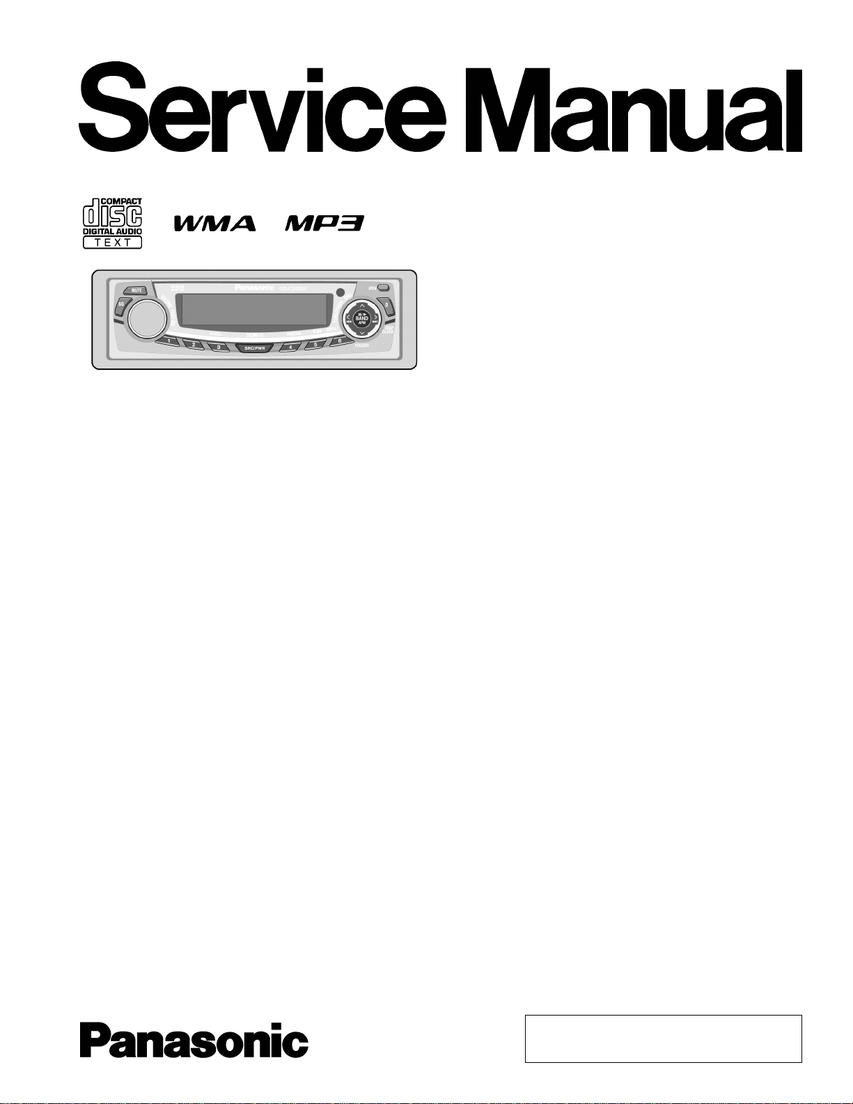
Panasonic CQC-3403-W Service manual
Specifications*
ORDER NO.ACED060110C3
AUTOMOTIVE AFTERMARKET
CQ-C3403W
WMA MP3 CD Player/Receiver
General
Power Supply DC 12V (11V - 16V),
Test Voltage 14.4V
Negative Ground
Current Consumption Less than 2.1A (CD mode ; 0.5W
4-channels)
Maximum Power Output 50W×4ch (at 1kHz)
Volume control maximum
Power Output 18W×4ch (1kHz, 1%, 4Ω)
Tone Adjustment Range Bass ; ±12dB at 100Hz
Treble ; ±12dB at 10kHz
Speaker Impedance 4-8Ω
Pre-Amp Output Voltage 2.5V (CD mode; 1kHz, 0dB)
Pre-Amp Output Impedance 200Ω
FM Stereo Radio
Frequency Range 87.5MHz - 108MHz
Usable Sensitivity 6dB/µV (S/N 30dB)
Frequency Response 30Hz-15kHz (±3dB)
Alternate Channel Selectivity 75dB
Stereo Separation 35dB (1kHz)
Image Rejection Ratio 70dB
IF Rejection Ratio 100dB
Signal to Noise Ratio 62dB
CD Player
Sampling Frequency 8 Times Oversampling
DA Converter 1bit DAC System
Pick-Up Type Astigma 3-beam
Light Source Semiconductor Laser
Wave Length 790nm
Frequency Response 20Hz to 20kHz (±1dB)
Signal to Noise Ratio 96dB
Total Harmonic Distortion 0.01% (1kHz)
Wow and Flutter Below measurable limits
Channel Separation 75dB
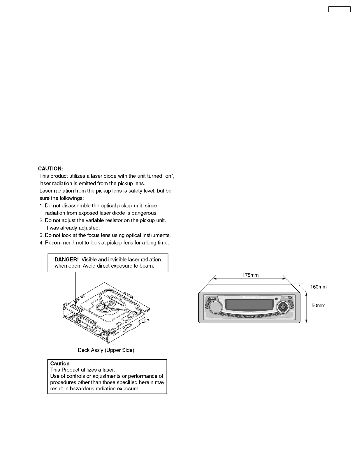
Dimensions** 178×50×160mm
Weight** 1.4kg
* Specifications and the design are subject to possible modification
without notice due to improvements.
** Dimensions and Weight shown are approximate.
•
• Above specifications comply with EIA standards.
• •
AM Radio
Frequency Range 531kHz - 1,602kHz
Usable Sensitivity 28dB/µV (S/N 20dB)
© 2006 Matsushita Electric Industrial Co., Ltd. All
rights reserved. Unauthorized copying and
distribution is a violation of law.
CQ-C3403W
CONTENTS
Page Page
1 ABOUT LEAD FREE SOLDER (PbF) 3
2 LASER PRODUCTS
3 FEATUERS
4 REPLACING THE FUSE
5 MAINTENANCE
6 NOTES
7 DIMENSIONS
8 WIRING CONNECTION
9 TERMINALS DESCRIPTION
10 PACKAGE AND IC BLOCK DIAGRAM
11 REPLACEMENT PARTS LIST
3
3
12 EXPLODE D VIEW (Unit)
3
13 CD PLAYER PARTS LIST
14 EXPLODE D VIEW (CD Deck)
3
3
15 WIRING DIAGRAM
3
16 SCHEMATIC DIAGRAM -1
17 SCHEMATIC DIAGRAM -2
4
5
18 BLOCK DIAGRAM
7
10
16
17
20
21
27
29
33
2
CQ-C3403W
1 ABOUT LEAD FREE
SOLDER (PbF)
Distinction of PbF PCB:
PCBs (manufactured) using lead free solder will have a PbF
stamp on the PCB.
Caution :
•
• Pb free solder has a higher melting point than standard
• •
solder; Typically the melting point is 50 - 70°F (30 40°C) higher. Please use a soldering iron with
temperature control and adjust it to 700 ± 20°F (370 ±
10°C). In case of using high temperature soldering iron,
please be careful not to heat too long.
•
• Pb free solder will tend to splash when heated too high
• •
(about 1100°F/600°C)
•
• This lead free solder will be used for the products after
• •
serial No. 1,000,001.
2 LASER PRODUCTS
3 FEATUERS
•
• The optional adapter allows you to connect the optional
• •
Panasonic CD changer unit (CX-DP880).
•
• The optional adapter allows you to connect the optional
• •
®
iPod
series.
•
• Hands Free Phone System. (The optional Bluetooth hands-
• •
free kit : CY-BT100N)
•
• Large-sized volume control.
• •
•
• SQ (Sound Quality).
• •
4 REPLACING THE FUSE
Use fuses of the same specified rating (15amps). Using
different substitutes or fuses with higher ratings, or connecting
the product directly without a fuse, could cause fire or damage
to the stereo unit.
5 MAINTENANCE
Your product is designed and manufactured to ensure a
minimum of maintenance. Use a dry, a soft cloth for routine
exterior cleaning. Never use benzine, thinner or other solvents.
6 NOTES
[RADIO BLOCK]
Do not align the AM/FM package block. When the package
block is necessary, it will be supplied already aligned at the
factory.
[CD DECK BLOCK]
This model has no servo alignment points because
microcomputer controls the servo circuit.
7 DIMENSIONS
3
CQ-C3403W
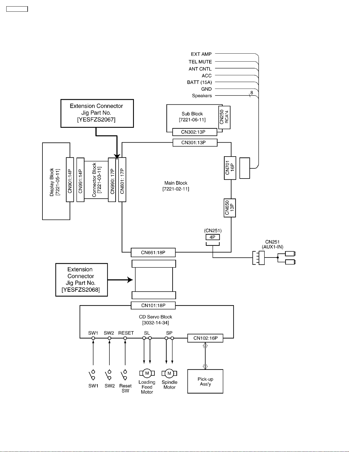
8 WIRING CONNECTION
4
9 TERMINALS DESCRIPTION
9.1. Main Block
IC601 : YESAM355
Pin
Port Description I/O (V)
No.
1 BATT DET Battery voltage detection I 1.9 1.9 1.9
2 SYSID 1 System upgrade ID1 I 4 4 4
3 SYSID 2 System upgrade ID2 I 4 4 4
4 PLL DO PLL data I 4.9 4.9 4.9
5 PLL CLK PLL data clock O 4.8 4.8 4.8
6 PLL DI PLL data O 0 0 0
7 PLL CE PLL chip select O 0 0 0
8 LED1 LED drive control 1 O 0 0 0
9 LED2 LED drive control 2 O 0 0 0
10 RESET Reset I 4.9 4.9 4.9
11 XT2 Crystal oscillator - 2.6 4.3 2.6
12 XT1 Crystal oscillator - 2.1 1.8 2
13 FLMD0
(NC)
14 X2 Crystal oscillator - 2.6 2.6 2.6
15 X1 Crystal oscillator - 2.4 2.4 2.4
16 REGC (Regulator capacitor) - 2.5 2.5 2.5
17 VSS Ground - 0 0 0
18 EVSS Ground - 0 0 0
19 VDD +5V power supply - 4.8 4.8 4.8
20 EVDD +5V power supply - 4.8 4.8 4.8
21 ROT 1 Rotary encoder input 1 I 4.8 4.8 4.8
22 ROT 2 Rotary encoder input 2 I 4.8 4.8 4.8
23 OP/CL Panel open/close detect I 4.7 4.7 4.7
24 (NC) - - - - 25 LED3 LED drive control 3 O 0 0 0
26 (NC) - - - - 27 PANEL Panel detection I 0 0 0
28 (NC) - - - - 29 (NC) - - - - 30 LCD 5V
CNT
31 LCD CE LCD chip enable O 0 0 0
32 EJECT EJECT switch I 4.9 4.9 4.9
33 EJ ILL LED control (EJ/ILL) O 4.7 4.7 4.7
34 AMP CNT Amp power control O 4.7 4.7 4.7
35 ANT CNT Antenna power control O 4.7 4.7 0
36 EXT.MUTEExternal mute O 4.9 4.9 4.9
37 (NC) - - - - 38 RM DATA Remote control data I 4.7 4.7 4.7
39 AF MUTE AF mute control O 4.7 4.7 4.7
40 INV CNT Illumination control O 4.7 4.7 4.7
41 (NC) - - - - 42 HUB ACC
CNT
43 INI A Mode setting A I 4.8 4.8 4.8
44 INI B Mode setting B I 0 0 0
45 INI C Mode setting C I 4.8 4.8 4.8
46 CHSTB /
SYSID4
47 CD MUTE CD mute I 0 0 0
48 EVENT System upgrade EVENT I 0 0 0
49 HUB CNT HUB control signal O 3.6 3.6 3.6
50 UART RX UART serial data I 0 0 0
51 UART TX UART serial data O 2.2 0 1.9
52 CD SI CD data input O 0 0 0
53 CD SO CD data output I 0 0 0.8
54 CD SCK CD clock O 4.7 4.7 4.7
55 CD RST CD reset O 4.7 4.7 4.7
56 CD STB CD strobe I 4.7 4.7 3.5
Display 5V control O 0 0 0
HUB ACC regulator control O 0 0 0
CD changer strobe /
System upgrade ID4
- - - - -
FM AM CD
I 0 0 0
Pin
Port Description I/O (V)
No.
57 (NC) - - - - 58 (NC) - - - - 59 AVREF (Conecting to +5V) - 4.9 4.9 4.9
60 AVSS Ground - 0 0 0
61 ACC ACC detection I 4.9 4.9 4.9
62 (NC) - - - - 63 LEVEL Audio level meter signal I 0 0 0
64 VSM Radio signal strength I 0 0 0
65 (NC) - - - - 66 SCL Audio control serial clock O 4.9 4.9 4.9
67 SDA Audio control data O 4.9 4.9 4.9
68 SD/ST Radio station detect I 4.8 4.8 4.8
69 MAIN CNT Main power control O 4.8 4.8 4.8
70 LCD CLK LCD Clock O 4.7 4.7 4.7
71 LCD DO LCD data I 4.7 4.7 4.7
72 LCD DI LCD data O 4.7 4.7 4.7
73 CH REM CD changer remote O 0 1.6 2.8
74 AMP
MUTE
75 STBY Power IC stundby control O 4.8 4.8 4.8
76 (NC) - - - - 77 CH DATA CD changer data I 0 0 0
78 CH CLK /
SYSID3
79 CD SW1 CD mechanism SW1 I 4.8 4.8 4.8
80 CD SW2 CD mechanism SW2 I 0 0 4.8
Amp mute control O 4.8 4.8 4.8
CD changer clock / System
upgrade ID3
FM AM CD
I 0 0 0
9.2. Display Block
IC901 : C0HBA0000195
Pin
No.
1-39 SEG1-39 LCD segment data O 2.4
40-43 COM1-4 LCD common O 2.4
44,45 SEG40,41 Not used - 46-49 KS3-6 Key scan O 4.7
50-54 Kl1-5 Key data I 0
55 TEST (Connecting to ground) - 0
56 VDD +5V power supply - 4.7
57 VDD1 VDD1 filter terminal - 3.1
58 VDD2 VDD2 filter terminal - 1.6
59 VSS Ground - 0
60 OSC Oscillator terminal - 3.7
61 DO Key data output O 4.7
62 CE LCD driver chip enable I 0
63 CLK LCD clock I 4.7
64 DI LCD data I 4.7
Port Description I/O (V)
CQ-C3403W
5

CQ-C3403W
9.3. CD Servo Block
IC101 : YESAM337
Pin No. Port Descriptions I/O (V)
1 AVSS GND - 0
2 LD-MT Loading Motor drive IC control 1 O 3.2
3 CNT Loading Motor drive IC control 2 O 3.2
4 - - - 5 LD-EJ Loading Motor drive IC control
(Eject)
6 AMUTE Mute signal output O 0
7 - - - 8 SBSY DSP IC SBSY O 0
9 - - - -
10 - - - 11 TXD0 Serial data output O 0
12 RXD0 Serial data input I 0
13 CLK0 Clock input I 2.9
14 - - - 15 - - - 16 - - - 17 AMD - - 3.2
18 DVCC Power supply (3.3V) - 3.2
19 X2 Crystal oscillator - 1.3
20 DVSS GND - 0
21 X1 Crystal oscillator - 1.3
22 AMI - - 3.2
23 RESET Reset I 3
24 - - - 25 - - - 26 NMI - - 3.2
27 - - - 28 STBY DSP IC STBY O 0
29 RST DSP IC RST O 3.2
30 CCE DSP IC CCE O 2.6
31 BUCK DSP IC CK O 2.8
32 BUS3 DSP IC BUS3 O 2.8
33 BUS2 DSP IC BUS2 O 2.8
34 BUS1 DSP IC BUS1 O 2.8
35 BUS0 DSP IC BUS0 O 2.9
36 RESETSWMechanics deck REST SW input I 3.2
Pin No. Port Descriptions I/O (V)
60 P50/AN0 Reference voltage I 0.3
61 P51/AN0 Loading motor detect I 2.1
62 P52/AN2 - - 0
63 P53/AN3 - - 0
64 AVCC Power supply (3.3V) - 3.2
O 0
37 SW1 Mechanics deck SW1 input I 0
38 SW2 Mechanics deck SW2 input I 0
39 CONT
(P13)
40 - - - 41 - - - 42 - - - 43 CONT
(P17)
44 PIO0 DSP IC PIO0 O 0
45 ZDET LOAD detect I 0
46 - - - 47 - - - 48 - - - 49 - - - 50 - - - 51 - - - 52 - - - 53 - - - 54 - - - 55 - - - 56 - - - 57 - - - 58 - - - 59 CDFS Serial frame sink signal input
DSP IC power control 1 O 3.2
DSP IC power control 2 O 3.2
I 2.3
(CD ON)
6
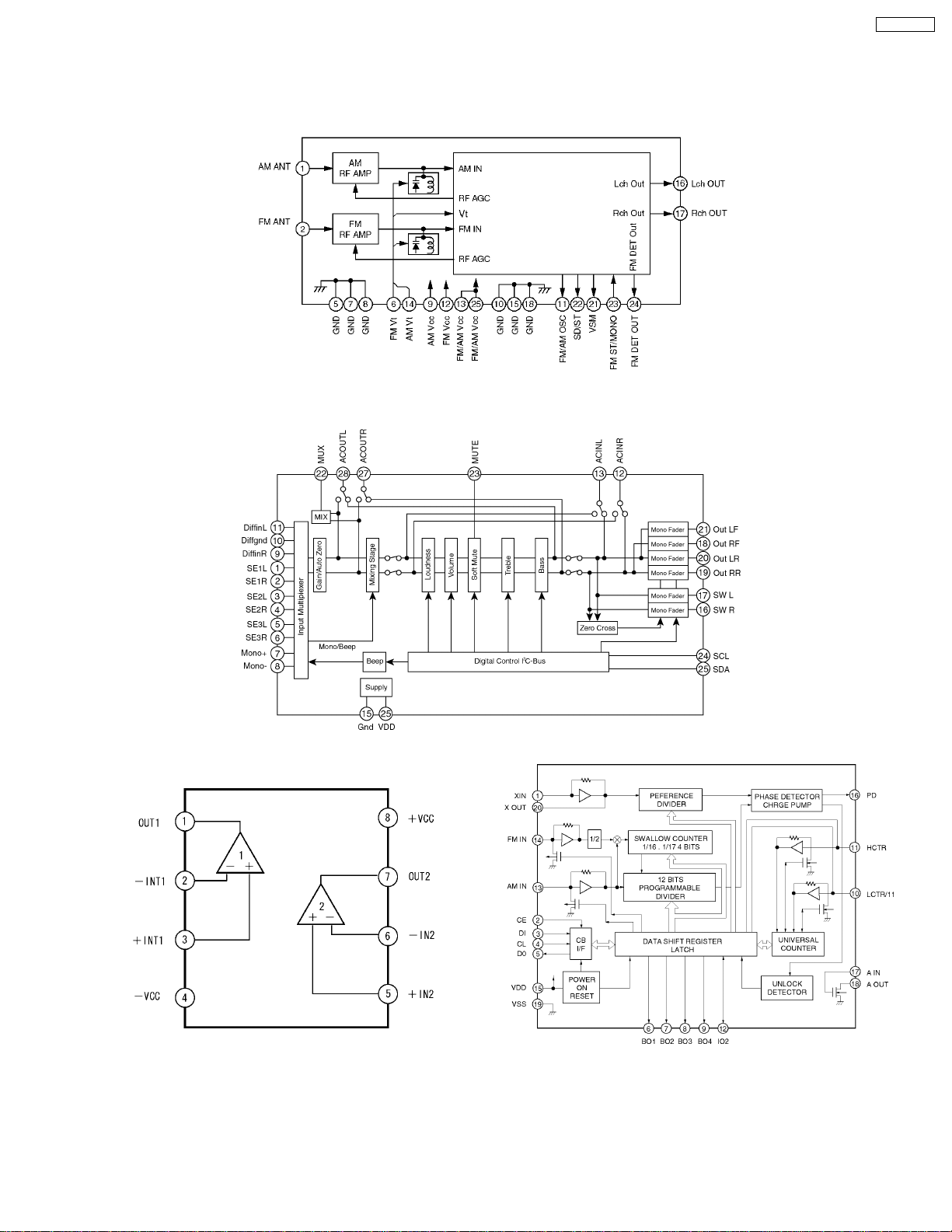
10 PACKAGE AND IC BLOCK DIAGRAM
10.1. Main Block
PA051 : YESAP403
CQ-C3403W
IC231 : C0ABBB000038
IC201 : YESAM293
IC401 : YESAM321
7
CQ-C3403W
IC271 : C1EA00000041
IC650 : YESAM265
IC681 : YESAM346
IC791 : YESAM344
IC750 : YESAM267
10.2. Display Block
IC710 : YESAM340
IC905 : YESAM264
8
10.3. CD Servo Block
IC401,403 : YESAM341
CQ-C3403W
IC402 : YESAM342
9
CQ-C3403W
11 REPLACEMENT PARTS
LIST
Notes :
1. Be sure to make your orders of replacement parts
according to this list.
2. Important safety notice: Components, identified by
have special characteristics important for safety. When
replacing any of these components, use only
manufacturer´s specified parts.
3. Location keys in the remarks column indicates the general
location of the parts shown in the exploded drawing, as in a
road map.
4. The marking (RTL) indicates that Retention Time is limited
for this item. After the discontinuation of assembly in
production, the item will continue to be available for a
specific period of time. The retention period of availability is
dependent on the type of assembly, and in accordance with
the laws governing part and product retention. After the end
of this period, the assembly will no longer be available.
•
• Order intake period is basically six months after the first
• •
shipment.
Ref. No. Part No. Part Name & Description Remarks
[7221-02-11] MAIN BLOCK
IC´s and TRANSISTORs
IC201 YESAM293 IC
IC231 C0ABBB000038 IC
IC271 C1EA00000041 IC
IC401 YESAM321 IC
IC601 YESAM355 IC (w/program)
IC650 YESAM265 IC
IC681 YESAM346 IC
IC710 YESAM340 IC
IC740 YESAM299 IC
IC750 YESAM267 IC
IC755 YESAM347 IC
IC791 YESAM344 IC
PA051 YESAP403 Tuner Pack
Q052 YESAN117 Transistor
Q055 YESAN117 Transistor
Q660 YESAN119 Transistor
Q671 YESAN118 Transistor
Q672 YESAN120 Transistor
Q681 YESAN123 Transistor
Q682 YESAN122 Transistor
Q683 YESAN122 Transistor
Q720 YESAN115 FET
Q721 YESAN123 Transistor
Q730 YESAN115 FET
Q731 YESAN123 Transistor
Q740 YESAN079 Transistor
Q751 YESAN079 Transistor
Q761 YESAN090 Transistor
Q770 YESAN088 Transistor
DIODEs
D053 YESAD119 Zener Diode
D245 YESAD155 Diode
D270 YESAD146 Diode
D271 YESAD146 Diode
D272 YESAD146 Diode
D273 YESAD146 Diode
D274 YESAD146 Diode
D275 YESAD146 Diode
D276 YESAD146 Diode
D277 YESAD146 Diode
D601 YESAD155 Diode
mark
Ref. No. Part No. Part Name & Description Remarks
D602 YESAD147 Zener Diode
D603 YESAD147 Zener Diode
D636 YESAD144 Diode
D637 YESAD143 Diode
D638 YESAD119 Zener Diode
D650 YESAD144 Diode
D652 YESAD119 Zener Diode
D654 YESAD119 Zener Diode
D655 YESAD119 Zener Diode
D701 YESAD139 Diode
D702 YESAD119 Zener Diode
D703 YESAD146 Diode
D705 YESAD119 Zener Diode
D710 YESAD144 Diode
D720 YESAD146 Diode
D721 YESAD146 Diode
D741 1SS133T77 Diode
D750 YESAD141 Diode
D760 YESAD146 Diode
D761 YESAD140 Diode
D770 YESAD123 Zener Diode
D790 YESAD143 Diode
CAPACITORs
C051 YECUS1H470JC Ceramic, 47pF 50WV
C053 YESCC482 Ceramic, 0.01µF 50WV
C055 YESCC482 Ceramic, 0.01µF 50WV
C057 YESCC482 Ceramic, 0.01µF 50WV
C058 YESCC482 Ceramic, 0.01µF 50WV
C061 YESCC527 Ceramic, 0.022µF 25WV
C062 YESCC527 Ceramic, 0.022µF 25WV
C065 YESCC481 Ceramic, 0.001µF 50WV
C067 YESCC482 Ceramic, 0.01µF 50WV
C203 YESCC550 Electrolytic, 3.3µF 50WV
C204 YESCC454 Ceramic, 2.2µF
C206 YESCC454 Ceramic, 2.2µF
C208 YESCC529 Ceramic, 0.22µF 16WV
C210 YESCC228 Ceramic, 0.1µF 16WV
C220 YESCC549 Electrolytic, 2.2µF 50WV
C234 YESCC228 Ceramic, 0.1µF 16WV
C235 YESCC526 Ceramic, 0.18µF 25WV
C237 YESCC530 Ceramic, 0.082µF 25WV
C238 YESCC545 Electrolytic, 22µF 10WV
C244 YESCC454 Ceramic, 2.2µF
C245 YESCC482 Ceramic, 0.01µF 50WV
C263 YESCC487 Ceramic, 0.47µF 16WV
C267 YESCC487 Ceramic, 0.47µF 16WV
C268 YESCC487 Ceramic, 0.47µF 16WV
C269 YESCC487 Ceramic, 0.47µF 16WV
C271 YESCC486 Ceramic, 0.0047µF 50WV
C272 YESCC486 Ceramic, 0.0047µF 50WV
C276 YESCC548 Electrolytic, 47µF 16WV
C277 YESCC452 Ceramic, 1µF 16WV
C278 YESCC228 Ceramic, 0.1µF 16WV
C279 YESCC368 Electrolytic, 2200µF 16WV
C295 YESCC454 Ceramic, 2.2µF
C296 YESCC454 Ceramic, 2.2µF
C303 YESCC550 Electrolytic, 3.3µF 50WV
C304 YESCC454 Ceramic, 2.2µF
C306 YESCC454 Ceramic, 2.2µF
C308 YESCC529 Ceramic, 0.22µF 16WV
C309 YESCC546 Electrolytic, 10µF 16WV
C310 YESCC313 Electrolytic, 220µF 10WV
C320 YESCC549 Electrolytic, 2.2µF 50WV
C339 YESCC527 Ceramic, 0.022µF 25WV
C363 YESCC487 Ceramic, 0.47µF 16WV
C367 YESCC487 Ceramic, 0.47µF 16WV
C368 YESCC487 Ceramic, 0.47µF 16WV
C369 YESCC487 Ceramic, 0.47µF 16WV
C371 YESCC486 Ceramic, 0.0047µF 50WV
C372 YESCC486 Ceramic, 0.0047µF 50WV
C375 YESCC546 Electrolytic, 10µF 16WV
C378 YESCC228 Ceramic, 0.1µF 16WV
10
Ref. No. Part No. Part Name & Description Remarks
C401 YESCC476 Ceramic, 18pF 50WV
C402 YESCC245 Ceramic, 12pF 50WV
C403 YESCC482 Ceramic, 0.01µF 50WV
C404 YESCC482 Ceramic, 0.01µF 50WV
C405 YESCC544 Electrolytic, 100µF 6.3WV
C409 YESCC543 Electrolytic, 680µF 10WV
C411 F1J1H101A667 Ceramic, 100pF 50WV
C412 F1J1H101A667 Ceramic, 100pF 50WV
C413 F1J1H101A667 Ceramic, 100pF 50WV
C414 YESCC551 Electrolytic, 4.7µF 50WV
C415 YESCC482 Ceramic, 0.01µF 50WV
C416 YESCC482 Ceramic, 0.01µF 50WV
C430 YESCC313 Electrolytic, 220µF 10WV
C602 YESCC378 Electrolytic, 1000µF 6.3WV
C605 YESCC452 Ceramic, 1µF 16WV
C606 YESCC487 Ceramic, 0.47µF 16WV
C607 YECUS1H470JC Ceramic, 47pF 50WV
C608 YECUS1H470JC Ceramic, 47pF 50WV
C609 YECUS1H470JC Ceramic, 47pF 50WV
C610 YECUS1H470JC Ceramic, 47pF 50WV
C611 YECUS1H470JC Ceramic, 47pF 50WV
C628 YESCC228 Ceramic, 0.1µF 16WV
C629 YECUS1H470JC Ceramic, 47pF 50WV
C631 YESCC483 Ceramic, 0.1µF 50WV
C632 YESCC377 Electrolytic, 47µF 6.3WV
C634 YESCC223 Ceramic, 27pF 50WV
C635 YECUS1H220JC Ceramic, 22pF 50WV
C636 YESCC454 Ceramic, 2.2µF
C637 YESCC481 Ceramic, 0.001µF 50WV
C638 YESCC454 Ceramic, 2.2µF
C650 YESCC483 Ceramic, 0.1µF 50WV
C651 YESCC482 Ceramic, 0.01µF 50WV
C652 YESCC482 Ceramic, 0.01µF 50WV
C655 F1J1H101A667 Ceramic, 100pF 50WV
C660 YESCC549 Electrolytic, 2.2µF 50WV
C661 YESCC567 Ceramic, 0.0027µF 50WV
C665 YESCC483 Ceramic, 0.1µF 50WV
C670 YESCC482 Ceramic, 0.01µF 50WV
C671 YESCC483 Ceramic, 0.1µF 50WV
C673 YESCC452 Ceramic, 1µF 16WV
C681 YESCC228 Ceramic, 0.1µF 16WV
C682 YESCC228 Ceramic, 0.1µF 16WV
C683 YESCC228 Ceramic, 0.1µF 16WV
C701 YESCC452 Ceramic, 1µF 16WV
C710 YESCC482 Ceramic, 0.01µF 50WV
C711 YESCC482 Ceramic, 0.01µF 50WV
C741 YESCC538 Electrolytic, 150µF 6.3WV
C751 YESCC368 Electrolytic, 2200µF 16WV
C752 YESCC539 Electrolytic, 120µF 10WV
C753 YESCC377 Electrolytic, 47µF 6.3WV
C755 YESCC228 Ceramic, 0.1µF 16WV
C756 YESCC482 Ceramic, 0.01µF 50WV
C757 YESCC228 Ceramic, 0.1µF 16WV
C770 YESCC547 Electrolytic, 100µF 16WV
C790 YESCC228 Ceramic, 0.1µF 16WV
C791 YESCC529 Ceramic, 0.22µF 16WV
C792 YESCC515 Electrolytic, 47µF 16WV
RESISTORs
J101 ERJ8GX0R00V Chip, 0Ω 1/8W
J103 ERJ8GX0R00V Chip, 0Ω 1/8W
J104 YESRG196 Chip, 0Ω 1/8W
J105 ERJ8GX0R00V Chip, 0Ω 1/8W
J106 ERJ8GX0R00V Chip, 0Ω 1/8W
J107 YESRG196 Chip, 0Ω 1/8W
J108 ERJ8GX0R00V Chip, 0Ω 1/8W
J109 YESRG196 Chip, 0Ω 1/8W
J110 ERJ8GX0R00V Chip, 0Ω 1/8W
J111 ERJ8GX0R00V Chip, 0Ω 1/8W
J112 ERJ8GX0R00V Chip, 0Ω 1/8W
J113 YESRG196 Chip, 0Ω 1/8W
J114 ERJ8GX0R00V Chip, 0Ω 1/8W
J116 YESRG196 Chip, 0Ω 1/8W
CQ-C3403W
Ref. No. Part No. Part Name & Description Remarks
J117 YESRG196 Chip, 0Ω 1/8W
J118 YESRG196 Chip, 0Ω 1/8W
J119 ERJ8GX0R00V Chip, 0Ω 1/8W
J120 ERJ8GX0R00V Chip, 0Ω 1/8W
J121 ERJ8GX0R00V Chip, 0Ω 1/8W
J201 YESRG132 Chip, 0Ω 1/4W
J202 YESRG132 Chip, 0Ω 1/4W
J203 YESRG132 Chip, 0Ω 1/4W
J204 YESRG132 Chip, 0Ω 1/4W
J205 YESRG132 Chip, 0Ω 1/4W
J206 YESRG132 Chip, 0Ω 1/4W
J207 YESRG132 Chip, 0Ω 1/4W
J208 ERJ8GX0R00V Chip, 0Ω 1/4W
J209 ERJ8GX0R00V Chip, 0Ω 1/4W
J210 ERJ8GX0R00V Chip, 0Ω 1/4W
J211 ERJ8GX0R00V Chip, 0Ω 1/4W
J212 ERJ8GX0R00V Chip, 0Ω 1/4W
J213 YESRG132 Chip, 0Ω 1/4W
J214 YESRG132 Chip, 0Ω 1/4W
J215 YESRG132 Chip, 0Ω 1/4W
J216 ERJ8GX0R00V Chip, 0Ω 1/4W
J217 YESRG132 Chip, 0Ω 1/4W
J218 YESRG132 Chip, 0Ω 1/4W
J219 YESRG132 Chip, 0Ω 1/4W
J220 ERJ8GX0R00V Chip, 0Ω 1/4W
J221 YESRG132 Chip, 0Ω 1/4W
J222 ERJ8GX0R00V Chip, 0Ω 1/4W
J223 ERJ8GX0R00V Chip, 0Ω 1/4W
J224 ERJ8GX0R00V Chip, 0Ω 1/4W
J226 YESRG132 Chip, 0Ω 1/4W
J227 ERJ8GX0R00V Chip, 0Ω 1/4W
J228 YESRG132 Chip, 0Ω 1/4W
J229 YESRG132 Chip, 0Ω 1/4W
J230 YESRG132 Chip, 0Ω 1/4W
J231 ERJ8GX0R00V Chip, 0Ω 1/4W
J232 YESRG132 Chip, 0Ω 1/4W
J233 YESRG132 Chip, 0Ω 1/4W
J234 ERJ8GX0R00V Chip, 0Ω 1/4W
J235 ERJ8GX0R00V Chip, 0Ω 1/4W
J236 ERJ8GX0R00V Chip, 0Ω 1/4W
J237 ERJ8GX0R00V Chip, 0Ω 1/4W
J238 YESRG132 Chip, 0Ω 1/4W
J239 YESRG132 Chip, 0Ω 1/4W
J240 ERJ8GX0R00V Chip, 0Ω 1/4W
J241 YESRG132 Chip, 0Ω 1/4W
J242 YESRG132 Chip, 0Ω 1/4W
J243 YESRG132 Chip, 0Ω 1/4W
J244 ERJ8GX0R00V Chip, 0Ω 1/4W
R050 YESRG399 Chip, 5.6kΩ 1/8W
R053 YESRG426 Chip, 120Ω 1/8W
R058 ERJ8GX0R00V Chip, 0Ω 1/8W
R059 YESRG361 Chip, 100kΩ 1/8W
R060 YESRG385 Chip, 33kΩ 1/8W
R065 YESRG387 Chip, 39kΩ 1/8W
R066 YESRG196 Chip, 0Ω 1/8W
R202 YESRG388 Chip, 4.3kΩ 1/8W
R203 YESRG385 Chip, 33kΩ 1/8W
R204 YESRG397 Chip, 5.6kΩ 1/8W
R205 YESRG406 Chip, 9.1kΩ 1/8W
R206 YESRG397 Chip, 5.6kΩ 1/8W
R207 YESRG406 Chip, 9.1kΩ 1/8W
R208 YESRG415 Chip, 18kΩ 1/8W
R209 YESRG338 Carbon, 100Ω 1/4W
R225 YESRG205 Carbon, 1kΩ 1/4W
R226 YESRG205 Carbon, 1kΩ 1/4W
R237 YESRG360 Chip, 10kΩ 1/8W
R237 YESRG360 Chip, 10kΩ 1/8W
R238 YESRG385 Chip, 33kΩ 1/8W
R239 YESRG361 Chip, 100kΩ 1/8W
R245 YESRG349 Chip, 22Ω 1/4W
R261 ERJ8GX0R00V Chip, 0Ω 1/8W
R262 ERJ8GX0R00V Chip, 0Ω 1/8W
R263 YESRG396 Chip, 560Ω 1/8W
R267 YESRG396 Chip, 560Ω 1/8W
11
CQ-C3403W
Ref. No. Part No. Part Name & Description Remarks
R275 YESRG376 Chip, 22kΩ 1/8W
R295 YESRG365 Chip, 130Ω 1/8W
R302 YESRG388 Chip, 4.3kΩ 1/8W
R303 YESRG385 Chip, 33kΩ 1/8W
R304 YESRG352 Chip, 5.6kΩ 1/4W
R305 YESRG354 Chip, 9.1kΩ 1/4W
R306 YESRG397 Chip, 5.6kΩ 1/8W
R307 YESRG406 Chip, 9.1kΩ 1/8W
R308 YESRG415 Chip, 18kΩ 1/8W
R309 YESRG338 Carbon, 100Ω 1/4W
R325 YESRG360 Chip, 10kΩ 1/8W
R326 YESRG360 Chip, 10kΩ 1/8W
R338 YESRG148 Chip, 47kΩ 1/4W
R361 ERJ8GX0R00V Chip, 0Ω 1/8W
R362 ERJ8GX0R00V Chip, 0Ω 1/8W
R363 YESRG396 Chip, 560Ω 1/8W
R367 YESRG396 Chip, 560Ω 1/8W
R375 YESRG364 Chip, 12kΩ 1/8W
R401 YESRG320 Chip, 2.2kΩ 1/8W
R402 YESRG320 Chip, 2.2kΩ 1/8W
R403 YESRG320 Chip, 2.2kΩ 1/8W
R404 YESRG320 Chip, 2.2kΩ 1/8W
R405 YESRG390 Chip, 4.7kΩ 1/8W
R406 ERJ8GX0R00V Chip, 0Ω 1/8W
R407 YESRG391 Chip, 47kΩ 1/8W
R408 YESRG391 Chip, 47kΩ 1/8W
R409 YESRG367 Chip, 1.5kΩ 1/8W
R412 YESRG391 Chip, 47kΩ 1/8W
R413 ERJ8GX0R00V Chip, 0Ω 1/8W
R416 YESRG384 Chip, 330Ω 1/8W
R417 YESRG367 Chip, 1.5kΩ 1/8W
R418 YESRG311 Chip, 2.7kΩ 1/4W
R419 YESRG367 Chip, 1.5kΩ 1/8W
R420 ERJ8GX0R00V Chip, 0Ω 1/8W
R601 YESRG134 Chip, 1kΩ 1/4W
R602 YESRG147 Chip, 4.7kΩ 1/4W
R603 YESRG319 Chip, 1kΩ 1/8W
R604 YESRG319 Chip, 1kΩ 1/8W
R605 YESRG319 Chip, 1kΩ 1/8W
R606 YESRG134 Chip, 1kΩ 1/4W
R607 YESRG205 Carbon, 1kΩ 1/4W
R608 YESRG360 Chip, 10kΩ 1/8W
R609 ERJ8GX0R00V Chip, 0Ω 1/8W
R610 YESRG139 Chip, 180kΩ 1/4W
R611 YESRG360 Chip, 10kΩ 1/8W
R612 YESRG359 Chip, 100Ω 1/8W
R613 YESRG361 Chip, 100kΩ 1/8W
R614 YESRG361 Chip, 100kΩ 1/8W
R615 YESRG319 Chip, 1kΩ 1/8W
R616 YESRG319 Chip, 1kΩ 1/8W
R617 YESRG319 Chip, 1kΩ 1/8W
R618 YESRG134 Chip, 1kΩ 1/4W
R619 ERJ8GX0R00V Chip, 0Ω 1/8W
R622 YESRG361 Chip, 100kΩ 1/8W
R623 YESRG361 Chip, 100kΩ 1/8W
R624 YESRG244 Carbon, 100kΩ 1/4W
R625 YESRG205 Carbon, 1kΩ 1/4W
R626 YESRG205 Carbon, 1kΩ 1/4W
R632 YESRG319 Chip, 1kΩ 1/8W
R633 YESRG319 Chip, 1kΩ 1/8W
R634 YESRG377 Chip, 220kΩ 1/8W
R636 YESRG319 Chip, 1kΩ 1/8W
R637 YESRG391 Chip, 47kΩ 1/8W
R638 YESRG360 Chip, 10kΩ 1/8W
R639 YESRG360 Chip, 10kΩ 1/8W
R640 YESRG382 Chip, 27kΩ 1/8W
R641 YESRG391 Chip, 47kΩ 1/8W
R644 YESRG391 Chip, 47kΩ 1/8W
R645 YESRG391 Chip, 47kΩ 1/8W
R648 YESRG391 Chip, 47kΩ 1/8W
R649 YESRG391 Chip, 47kΩ 1/8W
R650 YESRG205 Carbon, 1kΩ 1/4W
R651 YESRG205 Carbon, 1kΩ 1/4W
R652 YESRG319 Chip, 1kΩ 1/8W
Ref. No. Part No. Part Name & Description Remarks
R653 YESRG396 Chip, 560Ω 1/8W
R654 YESRG134 Chip, 1kΩ 1/4W
R655 YESRG319 Chip, 1kΩ 1/8W
R656 YESRG134 Chip, 1kΩ 1/4W
R657 YESRG319 Chip, 1kΩ 1/8W
R658 ERJ8GX0R00V Chip, 0Ω 1/8W
R660 YESRG041 Chip, 270Ω 1/4W
R661 YESRG397 Chip, 5.6kΩ 1/8W
R662 YESRG391 Chip, 47kΩ 1/8W
R663 ERJ8GX0R00V Chip, 0Ω 1/8W
R664 ERJ8GX0R00V Chip, 0Ω 1/8W
R665 YESRG391 Chip, 47kΩ 1/8W
R666 YESRG148 Chip, 47kΩ 1/4W
R667 YESRG148 Chip, 47kΩ 1/4W
R668 YESRG391 Chip, 47kΩ 1/8W
R669 YESRG134 Chip, 1kΩ 1/4W
R670 YESRG208 Carbon, 47kΩ 1/4W
R672 YESRG391 Chip, 47kΩ 1/8W
R673 YESRG319 Chip, 1kΩ 1/8W
R674 YESRG389 Chip, 470Ω 1/8W
R675 YESRG389 Chip, 470Ω 1/8W
R676 YESRG389 Chip, 470Ω 1/8W
R677 YESRG319 Chip, 1kΩ 1/8W
R678 YESRG373 Chip, 180kΩ 1/8W
R679 YESRG319 Chip, 1kΩ 1/8W
R680 YESRG389 Chip, 470Ω 1/8W
R681 YESRG389 Chip, 470Ω 1/8W
R682 YESRG389 Chip, 470Ω 1/8W
R683 YESRG389 Chip, 470Ω 1/8W
R684 YESRG319 Chip, 1kΩ 1/8W
R685 YESRG319 Chip, 1kΩ 1/8W
R686 YESRG150 Chip, 5.6Ω 1/4W
R687 YESRG391 Chip, 47kΩ 1/8W
R688 YESRG391 Chip, 47kΩ 1/8W
R690 YESRG205 Carbon, 1kΩ 1/4W
R691 YESRG360 Chip, 10kΩ 1/8W
R692 YESRG381 Chip, 2.7kΩ 1/8W
R693 YESRG381 Chip, 2.7kΩ 1/8W
R694 YESRG319 Chip, 1kΩ 1/8W
R695 YESRG381 Chip, 2.7kΩ 1/8W
R696 YESRG394 Chip, 5.1kΩ 1/8W
R697 YESRG394 Chip, 5.1kΩ 1/8W
R698 YESRG219 Chip, 5.1kΩ 1/4W
R699 YESRG217 Chip, 1.8kΩ 1/4W
R701 YESRG207 Carbon, 3.3kΩ 1/4W
R702 YESRG366 Chip, 13kΩ 1/8W
R704 YESRG362 Chip, 11kΩ 1/8W
R710 YESRG410 Chip, 200kΩ 1/8W
R711 YESRG414 Chip, 620kΩ 1/8W
R712 YESRG413 Chip, 30kΩ 1/8W
R713 YESRG134 Chip, 1kΩ 1/4W
R714 YESRG319 Chip, 1kΩ 1/8W
R717 YESRG409 Chip, 2kΩ 1/8W
R718 ERJ8GX0R00V Chip, 0Ω 1/8W
R722 YESRG191 Chip, 22kΩ 1/4W
R723 YESRG404 Chip, 8.2kΩ 1/8W
R724 YESRG388 Chip, 4.3kΩ 1/8W
R725 YESRG191 Chip, 22kΩ 1/4W
R730 YESRG388 Chip, 4.3kΩ 1/8W
R731 YESRG404 Chip, 8.2kΩ 1/8W
R740 YESRG136 Chip, 100k Ω 1/4W
R750 YESRG132 Chip, 0Ω 1/4W
R751 YESRG148 Chip, 47kΩ 1/4W
R752 YESRG367 Chip, 1.5kΩ 1/8W
R753 ERJ8GX0R00V Chip, 0Ω 1/8W
R760 YESRG319 Chip, 1kΩ 1/8W
R761 YESRG337 Chip, 3.3kΩ 1/8W
R762 YESRG319 Chip, 1kΩ 1/8W
R763 YESRG132 Chip, 0Ω 1/4W
R770 YESRG319 Chip, 1kΩ 1/8W
R790 YESRG389 Chip, 470Ω 1/8W
R791 YESRG411 Chip, 2.4kΩ 1/8W
R792 YESRG412 Chip, 27kΩ 1/8W
12
Ref. No. Part No. Part Name & Description Remarks
CONNECTORs
CN251 YESAJ07031 RCA Wire (AUX1-IN)
CN601 YESAE404 Connector, 17P
CN650 YESAE411 Connector, 13P
CN651 YESAJ07032 Connector w/ shield wire
CN661 YESAE410 Connector, 18P
CN701 YESAE351 Connector 16P
RESISTOR NETWORK
RA602 YESXB017 Registor Network, 1kΩ *4
COILs
L051 YESLQ035 Inductor
L052 YESLQ028 Inductor
L401 YESLQ017 Inductor
L402 YESLQ017 Inductor
L601 YESLQ045 Inductor
L602 YESLQ045 Inductor
L680 YESLQ027 Inductor
L701 YESLT030 Inductor
L710 YESLQ012 Inductor
L770 YESLQ045 Inductor
CRYSTALs
XL401 YESXL034 Crystal
XL601 YESXL035 Crystal
XL602 YESXL036 Crystal
POSISTOR
PH701 YESRTD011 Posistor
CQ-C3403W
Ref. No. Part No. Part Name & Description Remarks
J204 ERJ8GX0R00V Chip, 0Ω 1/4W
J206 ERJ8GX0R00V Chip, 0Ω 1/4W
J207 ERJ8GX0R00V Chip, 0Ω 1/4W
J209 ERJ8GX0R00V Chip, 0Ω 1/4W
J210 YESRG132 Chip, 0Ω 1/4W
J211 YESRG132 Chip, 0Ω 1/4W
R260 YESRG241 Chip, 0Ω 1/8W
R261 YESRG241 Chip, 0Ω 1/8W
R262 YESRG138 Chip, 180Ω 1/4W
R264 YESRG371 Chip, 180Ω 1/8W
R265 YESRG360 Chip, 10kΩ 1/8W
R266 YESRG360 Chip, 10kΩ 1/8W
R268 YESRG370 Chip, 18Ω 1/8W
R269 YESRG348 Chip, 18Ω 1/4W
R360 YESRG241 Chip, 0Ω 1/8W
R361 YESRG241 Chip, 0Ω 1/8W
R362 YESRG371 Chip, 180Ω 1/8W
R364 YESRG371 Chip, 180Ω 1/8W
R365 YESRG360 Chip, 10kΩ 1/8W
R366 YESRG360 Chip, 10kΩ 1/8W
R368 YESRG370 Chip, 18Ω 1/8W
R369 YESRG370 Chip, 18Ω 1/8W
CONNECTORs
CN250 YESAE412 Jack, RCA * 4
CN302 YESAE407 Connector, 13P
[7221-05-11] DISPLAY BLOCK
IC´s
IC901 C0HBA0000195 IC
IC905 YESAM264 IC
SERGE PROTECTOR / VARISTOR
Z050 YESRTD014 Serge Protector
Z701 YESRTD012 Varistor
SWITCH
SW670 YEAS08042 Switch
[7221-06-11] SUB BLOCK
TRANSISTORs
Q260 YESAN118 Transistor
Q261 YESAN121 Transistor
Q262 YESAN118 Transistor
Q263 YESAN121 Transistor
Q360 YESAN118 Transistor
Q361 YESAN121 Transistor
Q363 YESAN118 Transistor
Q364 YESAN121 Transistor
CAPACITORs
C264 YESCC536 Electrolytic, 4.7µF 25WV
C265 YESCC536 Electrolytic, 4.7µF 25WV
C291 YESRG196 Chip, 0Ω 1/8W
C364 YESCC536 Electrolytic, 4.7µF 25WV
C365 YESCC536 Electrolytic, 4.7µF 25WV
RESISTORs
J101 YESRG241 Chip, 0Ω 1/8W
J102 YESRG241 Chip, 0Ω 1/8W
J104 YESRG241 Chip, 0Ω 1/8W
J105 YESRG241 Chip, 0Ω 1/8W
J201 YESRG132 Chip, 0Ω 1/4W
J203 ERJ8GX0R00V Chip, 0Ω 1/4W
DIODEs
D901 YESAD166 LED
D902 YESAD170 LED
D903 YESAD170 LED
D904 YESAD170 LED
D906 YESAD170 LED
D907 YESAD170 LED
D908 YESAD170 LED
D909 YESAD170 LED
D910 YESAD170 LED
D911 YESAD170 LED
D912 YESAD170 LED
D913 YESAD170 LED
D914 YESAD170 LED
D915 YESAD170 LED
D920 YESAD168 LED
D921 YESAD168 LED
D931 YESAD150 Zener Diode
D932 YESAD167 Diode
D933 YESAD147 Zener Diode
D934 YESAD150 Zener Diode
D938 YESAD119 Zener Diode
CAPACITORs
C905 YESCC523 Ceramic, 0.1µF 16WV
C906 YESCC441 Ceramic, 1000pF 50WV
C914 YESCC523 Ceramic, 0.1µF 16WV
C915 YESCC523 Ceramic, 0.1µF 16WV
C916 YESCC523 Ceramic, 0.1µF 16WV
C922 YESCC532 Ceramic, 47pF 50WV
C923 YESCC542 Ceramic, 680pF
RESISTORs
R903 YESRG358 Chip, 470Ω 1/10W
R904 YESRG222 Chip, 1kΩ 1/10W
R905 YESRG222 Chip, 1kΩ 1/10W
13
 Loading...