

Panasonic CQC-1301-U, CQC-1401-U Service manual
Specifications*
ORDER NO. ACED041180C7
C4
AUTOMOTIVE AFTERMARKET
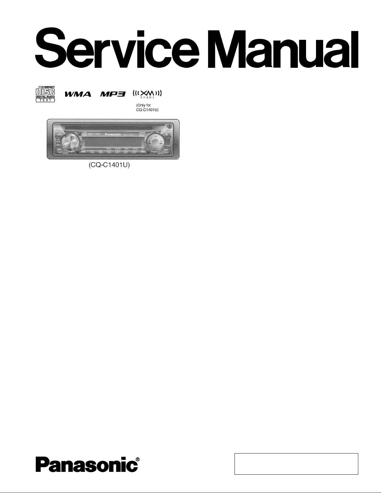
CQ-C1401U
CQ-C1301U
WMA MP3 CD Player/Receiver with CD
Changer Control
General
Power Supply DC 12V (11V - 16V),
Test Voltage 14.4V
Negative Ground
Current Consumption Less than 2.2A (CD mode ; 0.5W
4-channels)
Maximum Power Output 50W×4ch (at 1kHz)
Tone Adjustment Range Bass ; ±12dB at 100Hz
Treble ; ±12dB at 10kHz
Speaker Impedance 4-8Ω
Pre-Amp Output Voltage 2.5V (CD play mode ; 1kHz 0dB)
Pre-Amp Output Impedance 200Ω
Subwoofer Output Voltage 2.5V (CQ-C1401U)
Subwoofer Output Impedance 200Ω (CQ-C1401U)
FM Stereo Radio
Frequency Range 87.9MHz - 107.9MHz
Usable Sensitivity 10.2dBf. (75Ω)
50dB Quieting Sensitivity 15.2dBf. (75Ω)
Frequency Response 30Hz-15kHz(±3dB)
Alternate Channel Selectivity 75dB
Stereo Separation 35dB(1kHz)
Image Rejection Ratio 55dB
IF Rejection Ratio 100dB
Signal to Noise Ratio 62dB
AM Radio
Frequency Range 530 - 1,710kHz
Usable Sensitivity 27dB/µV (S/N 20dB)
CD Player
Sampling Frequency 8 Times Oversampling
DA Converter 1bit DAC System
Pick-Up Type Astigma 3-beam
Light Source Semiconductor Laser
Wave Length 790nm
Frequency Response 20Hz to 20,000Hz (±1dB)
Signal to Noise Ratio 96dB
Total Harmonic Distortion 0.01%(1kHz)
Wow and Flutter Below measurable limits
Channel Separation 75dB
Dimensions** 7”×1-15/16”×6-5/16”
(178×50×160mm)
Weight** 2lbs 14oz (1.3kg)
* Specifications and the design are subject to possible modification
without notice due to improvements.
** Dimensions and Weight shown are approximate.
•
• Above specifications comply with EIA standards.
• •
© 2004 Matsushita Electric Industrial Co., Ltd. All
rights reserved. Unauthorized copying and
distribution is a violation of law.
CQ-C1401U / CQ-C1301U
CONTENTS
Page Page
1 ABOUT LEAD FREE SOLDER (PbF) 3
2 LASER PRODUCTS
3 FEATUERS
4 REPLACING THE FUSE
5 MAINTENANCE
6 NOTES
7 DIMENSIONS
8 WIRING CONNECTION
9 TERMINALS DESCRIPTION
10 PACKAGE AND IC BLOCK DIAGRAM
11 PACKING PARTS LIST 11
12 REPLACEM ENT PARTS LIST [CQ-C1401U]
3
3
13 EXPLODE D VIEW (Unit) [CQ-C1401U]
3
14 REPLACEM ENT PARTS LIST [CQ-C1301U]
15 EXPLODE D VIEW (Unit) [CQ-C1301U]
3
3
16 CD PLAYER PARTS LIST
3
17 EXPLODED VIEW (CD Deck)
18 WIRING DIAGRAM
4
5
19 SCHEMAT IC DIAGRAM
8
20 BLOCK DIAGRAM
12
16
17
21
22
25
26
31
35
2
CQ-C1401U / CQ-C1301U
1 ABOUT LEAD FREE
SOLDER (PbF)
Distinction of PbF PCB:
PCBs (manufactured) using lead free solder will have a PbF
stamp on the PCB.
Caution :
•
•
Pb free solder has a higher melting point than standard
• •
solder; Typically the melting point is 50 - 70°F (30 40°C) higher. Please use a soldering iron with
temperature control and adjust it to 700 ± 20°F (370 ±
10°C). In case of using high temperature soldering iron,
please be careful not to heat too long.
•
•
Pb free solder will tend to splash when heated too high
• •
(about 1100°F/600°C)
•
•
This lead free solder will be used for the products after
• •
serial No. 1,000,001.
2 LASER PRODUCTS
3 FEATUERS
•
•
Digital servo for reliable playback.
• •
•
•
PLL (Phase Locked Loop) synthesized tuning.
• •
•
•
18-FM, 6-AM presets with preset scan.
• •
•
•
Removable face plate.
• •
•
•
MP3/WMA Playback from CD-R/RW.
• •
•
•
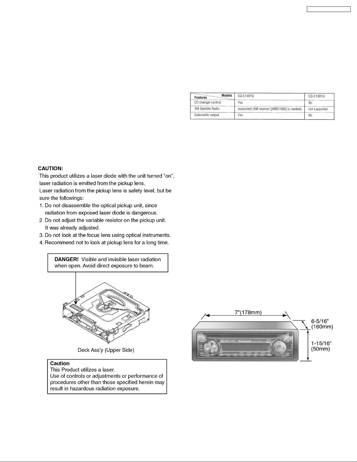
CD Changer Control. (CQ-C1401U)
• •
•
•
The following table describes the differences between
• •
2 models
4 REPLACING THE FUSE
Use fuses of the same specified rating (15amps). Using
different substitutes or fuses with higher ratings, or connecting
the product directly without a fuse, could cause fire or damage
to the stereo unit.
5 MAINTENANCE
Your product is designed and manufactured to ensure a
minimum of maintenance. Use a dry, a soft cloth for routine
exterior cleaning. Never use benzine, thinner or other solvents.
6 NOTES
[RADIO BLOCK]
Do not align the AM/FM package block. When the package
block is necessary, it will be supplied already aligned at the
factory.
[CD DECK BLOCK]
This model has no servo alignment points because
microcomputer controls the servo circuit.
7 DIMENSIONS
3
CQ-C1401U / CQ-C1301U
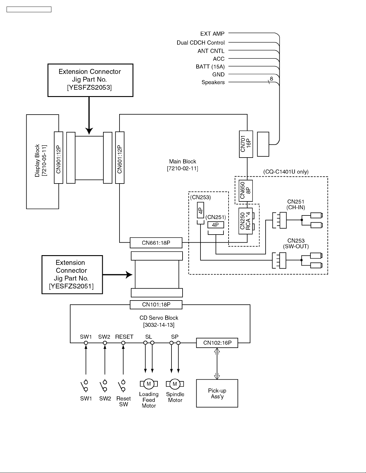
8 WIRING CONNECTION
4
9 TERMINALS DESCRIPTION
CQ-C1401U / CQ-C1301U
9.1. Main Block
IC601 : YESAM276
Pin
No.
1 (NC) - - - - 2 VSM Radio signal strength I 0 0 0
3 SD/ST Radio station detect I 0.3 0 0.8
4 AVSS Ground - 0 0 0
5 SCL Audio control serial clock O 4.9 4.9 4.9
6 SDA Audio control data O 4.9 4.9 4.9
7 AVREF (Conecting to +5V) - 4.9 4.9 4.9
8 CD SO CD data output I 2.1 2.3 1.7
9 CD SI CD data input O 0 0 3.3
10 CD SCK CD clock O 4.7 4.7 4.7
11 CDC DATA/
12 XM-RX SI XM radio RX signal O 4.8 4.8 4.8
13 CDC CLK CD changer clock I 0 0 0
14 CDC REM CD changer remote O 4.8 4.8 4.8
15 BZ OUT (NC) - - - - 16 LCD DO LCD data I 4.8 4.8 4.8
17 LCD DI LCD data O 4.7 4.7 4.7
18 LCD CLK LCD Clock O 4.8 4.8 4.8
19 CD MUTE CD mute I 0 0 4.8
20 CD RST CD reset O 4.8 4.8 4.8
21 CD STB CD strobe I 3.7 3.7 3.7
22 CDC SENS
23 PLL DO PLL data I 4.9 4.9 4.9
24 PLL CLK PLL data clock O 4.8 4.8 4.8
25 PLL DI PLL data O 0 0 0
26 PLL CE PLL chip select O 0 0 0
27 (NC) - - - - 28 (NC) - - - - 29 (NC) - - - - 30 (NC) - - - - 31 (NC) - - - - 32 (NC) - - - - 33 VSS1 Ground - 0 0 0
34 RDS DATA
35 S-LED (NC) - - - - 36 LCD CE LCD chip enable O 0 0 0
37 LCD 5V CNT Display 5V control O 0 0 0
38 (NC) - - - - 39 (NC) - - - - 40 (NC) - - - - 41 (NC) - - - - 42 ROTARY 1 Rotary encoder input 1 I 4.8 4.8 4.8
43 ROTARY 2 Rotary encoder input 2 I 4.7 4.7 4.7
44 (NC) - - - - 45 (NC) - - - - 46 PANEL Panel detection I 4.6 4.6 4.6
47 STBY Power IC stundby control O 4.8 4.8 4.8
48 EEPROM CE
49 EEPROM SK
50 EEPROM DI
51 EEPROM DO
52 (NC) - - - - 53 INV CNT Illumination control O 4.8 4.8 4.8
54 AMP CNT Amp power control O 4.8 4.8 4.8
Port Description I/O (V)
XM-TX SO
(NC)
(NC)
(NC)
(NC)
(NC)
(NC)
CD changer data/XM
radio TX signal
- - - - -
- - - - -
- - - - -
- - - - -
- - - - -
- - - - -
FM AM CD
I 0 0 0
Pin
No.
55 ANT CNT Antenna power control O 4.8 4.8 4.8
56 EXT.MUTE External mute O 4.8 4.8 4.8
57 MAIN CNT Main power control O 4.8 4.8 4.8
58 AMP MUTE Amp mute control O 4.8 4.8 4.8
59 AF MUTE AF mute control O 4.8 4.8 4.8
60 RESET Reset I 4.8 4.8 4.8
61 RDS CLK (NC) - - - - 62 (NC) - - - - 63 (NC) - - - - 64 RM DATA Remote control data I 4.8 4.8 4.8
65 BATT Battery voltage detection I 4.5 4.5 4.5
66 CDC STB/
67 VSS0 Ground - 0 0 0
68 VDD1 +5V power supply - 4.8 4.8 4.8
69 X2 Crystal oscillator - 2.9 2.9 2.9
70 X1 Crystal oscillator - 2.3 2.3 2.3
71 TEST (TEST terminal) - 0 0 0
72 XT2 Crystal oscillator - 2.7 2.7 2.7
73 XT1 Crystal oscillator - 2 2 2
74 VDD0 +5V power supply - 4.9 4.9 4.9
75 AVDD +5V power supply - 4.8 4.8 4.8
76 INI A Mode setting A I 0 0 0
77 INI B Mode setting B I 4.8 4.8 4.8
78 ACC ACC detection I 4.9 4.9 4.9
79 (NC) (Connecting to ground) - 0 0 0
80 LEVEL (Connecting to ground) - 0 0 0
Port Description I/O (V)
XM DET
CD Changer strobe/ XM
receiver detection
FM AM CD
I 4.8 4.8 4.8
9.2. Display Block
IC901 : YEAMLC75854T
Pin
No.
1-35 SEG1-35 LCD segment data O 2.5
36-39 NC - - 40-43 COM1-4 LCD common O 2.5
44 KS1 Not used - 45-49 KS2-6 Key scan O 5.0
50-54 Kl1-5 Key data I 0
55 TEST (Connecting to ground) - 0
56 VDD +5V power supply - 5.0
57 VDD1 VDD1 filter terminal - 3.3
58 VDD2 VDD2 filter terminal - 1.7
59 VSS Ground - 0
60 OSC Oscillator terminal - 3.9
61 DO Key data output O 5.0
62 CE LCD driver chip enable I 0
63 CLK LCD clock I 4.9
64 DI LCD data I 4.9
Port Description I/O (V)
5
CQ-C1401U / CQ-C1301U
9.3. CD Servo Block
IC401 : YESAM275
Pin
No.
Port Descriptions I/O (V)
1 CVSS1 GND - 0
2 - - - 3 CVSS2 GND - 0
4 DVDD1 I/O system (3.3V) power supply - 3.3
5 A10 Address bus of FLASH ROM O 0
6 - - - 7 A11 Address bus of FLASH ROM O 3.3
8 A12 O 3.3
9 A13 O 3.3
10 A14 O 3.3
11 A15 O 3.3
12 /CVDD1 CORE CPU system (1.6V) power
supply
13 - - - 14 DVSS1 GND - 0
15 CVSS3 GND - 0
16 /CVDD2 I/O system (3.3V) power supply - 1.6
17 - - - 18 - - - 19 READY - - 3.3
20 /PS FLASH ROM selection signal O 3.3
21 - - - 22 - - - 23 R/W Lead/light signal to FLASH ROM O 3.3
24 /MSTRB Memory access signal O 3.3
25 - - - 26 /MSC - - 3.3
27 MUTE Mute signal output (H:Mute on) O 0
28 - - - 29 - - - 30 /HOLD - - 3.3
31 BIO SUBO input I 0
32 MP/MC Operation mode setting (external pull-
up)
33 DVDD2 I/O system (3.3V) power supply - 3.3
34 CVSS4 GND - 0
35 BD R1 GND I 0
36 - - - 37 CVSS5 GND - 0
38 - - - 39 - - - 40 DVSS2 GND - 0
41 CLK C M AUDIO bit clock input I 1.6
42 SCK Clock input I 3.3
43 LRCK CMAUDIO L/R identifying signal input I 1.6
44 CDFS Serial frame sink signal input I 2.6
45 DATACMAUDIO serial data input I 1.6
46 - - - 47 SI Serial data input I 0
48 CLK M C AUDIO bit clock output O 1.6
49 SCK Clock input I 3.3
50 CVSS6 GND - 0
51 - - - 52 CVDD3 CORE CPU system (1.6V) power
supply
53 LRCK MCAUDIO L/R identifying signal output O 1.6
54 CDFS Serial frame sink signal input I 2.4
55 - - - 56 DVDD3 I/O system (3.3V) power supply - 3.3
57 DVSS3 GND - 0
- 1.6
I 3.3
- 1.6
Pin
No.
100 D1 I/O 0
101 D2 I/O 0
102 D3 I/O 0
103 D4 I/O 0
104 D5 I/O 0
105 A16 Address bus of FLASH ROM O 0
106 DVSS7 GND - 0
107 A17 Address bus of FLASH ROM O 3.3
108 A18 O 0
109 A19 Address bus of FLASH ROM O 0
110 A20 O 0
111 CVSS9 GND - 0
112 DVDD5 I/O system (3.3V) power supply - 3.3
113 D6 Data bus of FLASH ROM I/O 0
114 D7 I/O 0
115 D8 I/O 0
116 D9 I/O 0
117 D10 I/O 0
Port Descriptions I/O (V)
58 RESTSWMechanics deck REST SW input I 3.3
59 DATA MCAUDIO serial data output O 1.6
60 SO Serial data output O 1.2
61 - - - 62 - - - 63 /NMI - - 3.3
64 /INT0 - - 3.3
65 /INT1 - - 3.3
66 BLKCK Subcode block clock pulse input I 0
67 /INT3 - - 3.3
68 CV DD4 CORE CPU system (1.6V) power
69 SW1 Mechanics deck SW1 input I 0
70 CVSS7 GND - 0
71 MCLK Clock output (To Servo DSP) O 3.3
72 DVSS4 GND - 0
73 MLD Command load signal output (To
74 MDATA Command data output (To Servo
75 DVDD4 I/O system (3.3V) power supply - 3.3
76 DVSS5 GND - 0
77 CLK MD1 Clock mode setting (L fixation) I 0
78 CLK MD2 Clock mode setting (H fixation) I 3.3
79 CLK MD3 Clock mode setting (L fixation) I 80 - - - 81 SW2 Mechanics deck SW2 input I 0
82 - - - 83 EMU0 - - 0
84 EMU/OF
F
85 TDO - - 3.3
86 TDI - - 0
87 /TRST - - 3.3
88 TCK - - 0
89 TMS - - 3.3
90 CVSS8 GND - 3.3
91 CVDD5 CORE CPU system (1.6V) power
92 HPIENA GND I 1.6
93 DVSS6 GND - 0
94 - - - 95 CLKENA Oscillation output Cainabl signal O 3.3
96 X1 Crystal Connection O 0
97 X2/CLKIN Crystal Connection I 0
98 RS Reset signal input I 1
99 D0 Data base of FLASH ROM I/O 3.4
supply
Servo DSP)
DSP)
- - 3.3
supply
- 1.6
I 3.3
O 3.3
- 0
6
Pin
Port Descriptions I/O (V)
No.
118 D11 Data bus of FLASH ROM I/O 0
119 D12 I/O 0
120 STAT Status signal input I 0.4
121 D13 Data path of FLASH ROM I/O 0
122 D14 I/O 0
123 D15 I/O 0
124 - - - 125 CVDD6 CORE CPU system (1.6V) power
- 1.6
supply
126 CVSS10 GND - 0
127 - - - 128 DVSS8 I/O system (3.3V) power supply - 0
129 - - - 130 DVDD6 I/O system (3.3V) power supply - 3.3
131 A0 Address bus of FLASH ROM O 0
132 A1 O 0
133 A2 O 3.3
134 A3 O 3.3
135 /RST Reset signal output(To Servo DSP) O 3.3
136 A4 Address bus of FLASH ROM O 3.3
137 A5 O 0
138 A6 O 3.3
139 A7 O 3.3
140 A8 O 0
141 A9 O 3.3
142 CVDD7 CORE CPU system (1.6V) power
- 1.6
supply
143 - - - 144 DVSS9 GND - 0
CQ-C1401U / CQ-C1301U
7

CQ-C1401U / CQ-C1301U
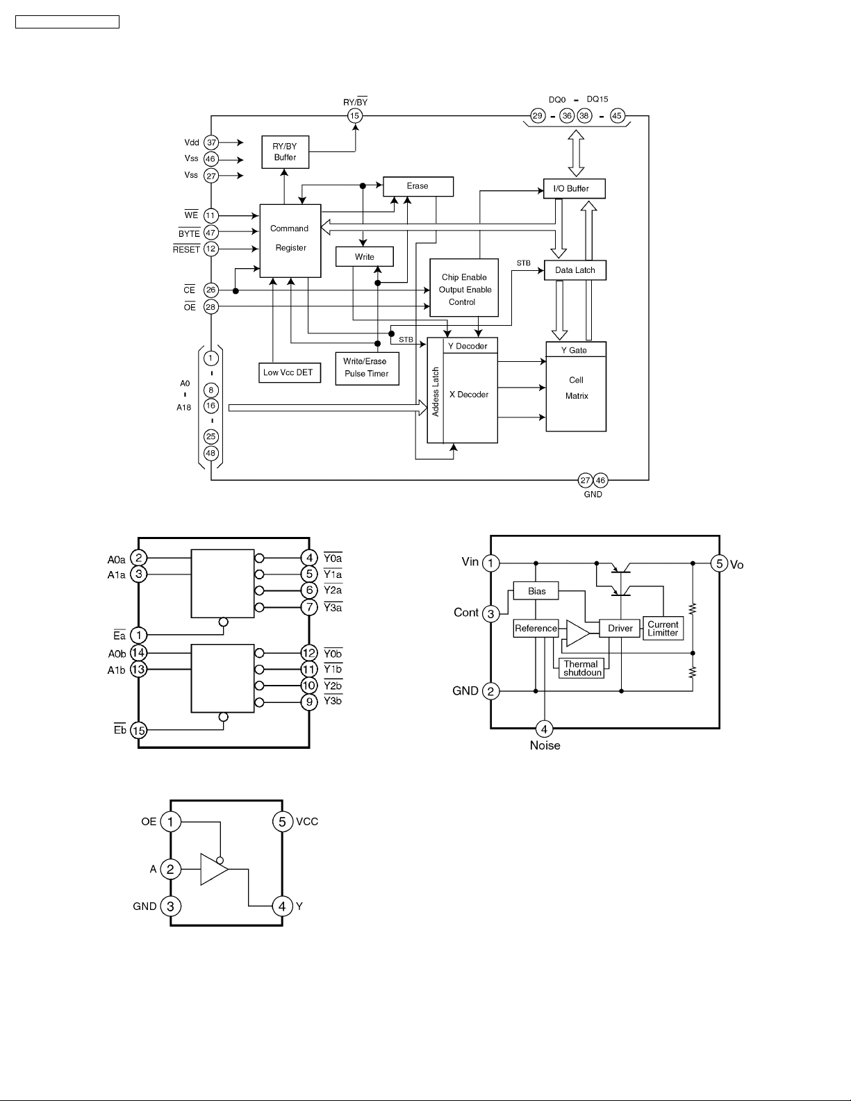
10 PACKAGE AND IC BLOCK DIAGRAM
10.1. Main Block
PA051 : YESAP387
IC201 : C1BB00000543
IC271 : YESAM274
8
IC401 : YESAM194
CQ-C1401U / CQ-C1301U
IC650 : YESAM265 (CQ-C1401U)
10.2. Display Block
IC902 : YESAM264
IC681 : YESAM273
9
CQ-C1401U / CQ-C1301U
10.3. CD Servo Block
IC403 : YESAM171
IC402 : YESAM271
IC404 : YESAM178
IC405 : YESAM270
10
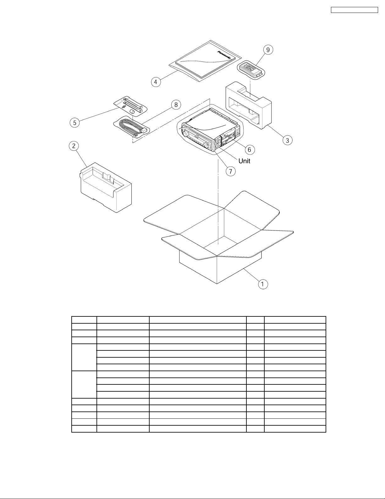
11 PACKING PARTS LIST
CQ-C1401U / CQ-C1301U
•
•
Item numbers listed below should not order regular spare parts.
• •
Item No. Part No. Part Name & Description Q´ty Remarks
1 — Inner Carton 1 Not available
2 — Packing Pad (Front) 1 Not available
3 — Packing Pad (Rear) 1 Not available
4 — Instruction Kit 1 Not available
— Operating Instructions (1) Not available
— Installation Instructions (1) Not available
— Owners Information Card (1) Not available
5 YEP0FZ5698 Installation Kit 1
— Lock Cancel Plate (2) Not available
— Mounting Bolt (1) Not available
— Rubber Bushing (1) Not available
6 YEFX0217263 Mounting Collar 1
7 YEFC05657 Trim plate 1
8 YESAJ01223 Power Connector 1
9 EUR7641010 Remote Control Unit (includes a battery) 1
(not available)
11
CQ-C1401U / CQ-C1301U
12 REPLACEMENT PARTS
LIST [CQ-C1401U]
Ref.
No.
Q770 YESAN088 Transistor
Part No. Part Name & Description Remarks
Notes :
1. Be sure to make your orders of replacement parts
according to this list.
2. Important safety notice: Components, identified by
mark
have special characteristics important for safety. When
replacing any of these components, use only
manufacturer´s specified parts.
3. Location keys in the remarks column indicates the general
location of the parts shown in the exploded drawing, as in a
road map.
4. The marking (RTL) indicates that Retention Time is limited
for this item. After the discontinuation of assembly in
production, the item will continue to be available for a
specific period of time. The retention period of availability is
dependent on the type of assembly, and in accordance with
the laws governing part and product retention. After the end
of this period, the assembly will no longer be available.
•
•
Order intake period is basically six months after the first
• •
shipment.
5. Reference materials of parts with the “TSN“ mark in the
remarks column are uploaded in the TSN (Technical
Service Navigation) system website. Please download from
that website for references.
Ref.
No.
[7210-02-11] MAIN BLOCK
IC´s and TRANSITORs
IC201 C1BB00000543 IC
IC231 YESAM268 IC
IC271 YESAM274 IC
IC401 YESAM194 IC
IC601 YESAM276 IC
IC650 YESAM265 IC
IC681 YESAM273 IC
IC710 YESAM277 IC
IC740 YESAM269 IC
IC750 YESAM267 IC
IC755 YESAM263 IC
PA051 YESAP387 Tuner Pack
Q052 YESAN082 Transistor
Q055 YESAN082 Transistor
Q262 YESAN085 Transistor
Q266 YESAN085 Transistor
Q346 YESAN085 Transistor
Q362 YESAN085 Transistor
Q366 YESAN085 Transistor
Q411 YEAN2SK536TB FET
Q660 YESAN081 Transistor
Q661 YESAN080 Transistor
Q662 YESAN080 Transistor
Q681 YESAN084 Transistor
Q720 YESAN089 FET
Q721 YESAN084 Transistor
Q722 YESAN089 FET
Q723 YESAN084 Transistor
Q730 YESAN089 FET
Q731 YESAN084 Transistor
Q740 YESAN079 Transistor
Q751 YESAN087 Transistor
Q761 YESAN090 Transistor
Part No. Part Name & Description Remarks
DIODEs
D270279
D650 YESAD144 Diode
D652 YESAD119 Zener Diode
D653 YESAD144 Diode
D671 YESAD143 Diode
D672 YESAD143 Diode
D683 YESAD115 Zener Diode
D684 YESAD115 Zener Diode
D685 YESAD115 Zener Diode
D689 YESAD115 Zener Diode
D701 YESAD139 Diode
D702 YESAD119 Zener Diode
D710 YESAD144 Diode
D720 YESAD146 Diode
D721 YESAD146 Diode
D740 YESAD146 Diode
D741 YESAD118 Diode
D750 YESAD141 Diode
D760 YESAD146 Diode
D761 YESAD140 Diode
D770 YESAD123 Zener Diode
D790 YESAD143 Diode
CPACITORs
C051 YECUS1H470JC Ceramic 47pF 50WV
C053 YECUS1H103KX Ceramic 0.01µF 50WV
C055 YECUS1H103KX Ceramic 0.01µF 50WV
C059 F1J1H101A025 Ceramic 100pF 50WV
C061 YESCC318 Ceramic 0.027µF 50WV
C062 YESCC318 Ceramic 0.027µF 50WV
C065 YECUS1H102KX Ceramic 0.001µF 50WV
C067 YECUS1H103KX Ceramic 0.01µF 50WV
C203 YESCC314 Electrolytic 3.3µF 50WV
C204 YESCC191 Ceramic 2.2µF 50WV
C208 YESCC199 Ceramic 0.33µF 16WV
C210 YESCC228 Ceramic 0.1µF 16WV
C220 YESCC375 Electrolytic 2.2µF 50WV
C235 YESCC284 Ceramic 0.18µF 50WV
C236 YESCC319 Ceramic 0.082µF 50WV
C237 YESCC284 Ceramic 0.18µF 50WV
C261 YESCC372 Electrolytic 4.7µF 25WV
C263 YECUS1C474KX Ceramic 0.47µF 16WV
C265 YESCC372 Electrolytic 4.7µF 25WV
C267 YECUS1C474KX Ceramic 0.47µF 16WV
C268 YECUS1C474KX Ceramic 0.47µF 16WV
C269 YECUS1C474KX Ceramic 0.47µF 16WV
C271 YECUS1H472KX Ceramic 0.0047µF 50WV
C272 YECUS1H472KX Ceramic 0.0047µF 50WV
C276 YESCC366 Electrolytic 10µF 16WV
C277 YESCC229 Ceramic 1µF 16WV
C278 YECUS1H104KX Ceramic 0.1µF 50WV
C279 YESCC368 Electrolytic 2200µF 16WV
C280 YESCC191 Ceramic 2.2µF 50WV
C281 YESCC191 Ceramic 2.2µF 50WV
C291 YECUS1H103KX Ceramic 0.01µF 50WV
C292 F1J1H101A025 Ceramic 100pF 50WV
C303 YESCC314 Electrolytic 3.3µF 50WV
C304 YESCC191 Ceramic 2.2µF 50WV
C308 YESCC199 Ceramic 0.33µF 16WV
C309 YESCC366 Electrolytic 10µF 16WV
YESAD146 Diode
12

Ref.
Part No. Part Name & Description Remarks
No.
C310 YESCC313 Electrolytic 220µF 10WV
C320 YESCC375 Electrolytic 2.2µF 50WV
C325 YECUS1H221JC Ceramic 220pF 50WV
C339 YECUS1H103KX Ceramic 0.01µF 50WV
C345 YESCC372 Electrolytic 4.7µF 25WV
C361 YESCC372 Electrolytic 4.7µF 25WV
C363 YECUS1C474KX Ceramic 0.47µF 16WV
C365 YESCC372 Electrolytic 4.7µF 25WV
C367 YECUS1C474KX Ceramic 0.47µF 16WV
C368 YECUS1C474KX Ceramic 0.47µF 16WV
C369 YECUS1C474KX Ceramic 0.47µF 16WV
C371 YECUS1H472KX Ceramic 0.0047µF 50WV
C372 YECUS1H472KX Ceramic 0.0047µF 50WV
C375 YESCC373 Electrolytic 0.47µF 50WV
C378 YECUS1H104KX Ceramic 0.1µF 50WV
C380 YECUS1H104KX Ceramic 0.1µF 50WV
C401 YESCC219 Ceramic 10pF 50WV
C402 F1J1H120A025 Ceramic 12pF 50WV
C403 YESCC376 Electrolytic 100µF 6.3WV
C405 F1J1H101A025 Ceramic 100pF 50WV
C411 YECUS1H103KX Ceramic 0.01µF 50WV
C412 YECUS1E223KX Ceramic 0.022µF 25WV
C413 ECQV1H224JL2 Plastic Film 0.22µF 50WV
C417 YESCC371 Electrolytic 680µF 16WV
C425 YECUS1H103KX Ceramic 0.01µF 50WV
C430 YESCC313 Electrolytic 220µF 10WV
C602 YESCC378 Electrolytic 1000µF 6.3WV
C605 YECUS1H103KX Ceramic 0.01µF 50WV
C628 YESCC228 Ceramic 0.1µF 16WV
C631 YESCC229 Ceramic 1µF 16WV
C634 YECUS1H220JC Ceramic 22pF 50WV
C635 YECUS1H220JC Ceramic 22pF 50WV
C650 YECUS1H103KX Ceramic 0.01µF 50WV
C660 YESCC375 Electrolytic 2.2µF 50WV
C672 YESCC377 Electrolytic 47µF 6.3WV
C681 YESCC228 Ceramic 0.1µF 16WV
C682 YECUS1H103KX Ceramic 0.01µF 50WV
C701 YESCC374 Electrolytic 01µF 50WV
C710 YESCC284 Ceramic 0.18µF 50WV
C711 YECUS1H103KX Ceramic 0.01µF 50WV
C740 YESCC369 Electrolytic 470µF 16WV
C741 YESCC379 Electrolytic 150µF 6.3WV
C751 YESCC370 Electrolytic 1000µF 16WV
C752 YESCC365 Electrolytic 120µF 10WV
C753 YESCC377 Electrolytic 47µF 6.3WV
C755 YESCC228 Ceramic 0.1µF 16WV
C756 YESCC380 Electrolytic 39µF 6.3WV
C770 YESCC367 Electrolytic 100µF 16WV
C771 F1J1H101A025 Ceramic 100pF 50WV
C790 YECUS1H104KX Ceramic 0.1µF 50WV
R771 F1J1H101A025 Ceramic 100pF 50WV
RESISTORs
J722 YESRG204 Carbon 560Ω 1/4W
J724 YESRG204 Carbon 560Ω 1/4W
J801-
YESRG132 Chip 0Ω 1/4W
821
J823-
YESRG132 Chip 0Ω 1/4W
829
J830 ERJ8GX0R00V Chip 0Ω 1/4W
J831-
YESRG132 Chip 0Ω 1/4W
835
J837-
YESRG132 Chip 0Ω 1/4W
840
J901 YESRG093 Chip 0Ω 1/8W
J902 YESRG093 Chip 0Ω 1/8W
Ref.
Part No. Part Name & Description Remarks
No.
J904 YESRG093 Chip 0Ω 1/8W
J906 YESRG093 Chip 0Ω 1/8W
L290 YESRG093 Chip 0Ω 1/8W
L291 YESRG093 Chip 0Ω 1/8W
L292 YESRG093 Chip 0Ω 1/8W
R050 YESRG127 Chip 5.6Ω 1/8W
R051 YESRG132 Chip 0Ω 1/4W
R052 YESRG094 Chip 100Ω 1/8W
R053 YESRG114 Chip 330Ω 1/8W
R058 YESRG093 Chip 0Ω 1/8W
R059 YESRG097 Chip 100kΩ 1/8W
R060 YESRG115 Chip 33kΩ 1/8W
R065 YESRG117 Chip 3.9kΩ 1/8W
R202 YESRG184 Chip 4.3kΩ 1/8W
R203 YESRG115 Chip 33kΩ 1/8W
R204 YESRG125 Chip 5.6kΩ 1/8W
R205 YESRG216 Chip 9.1kΩ 1/8W
R208 YESRG202 Chip 18kΩ 1/4W
R225 YESRG205 Carbon 1kΩ 1/4W
R226 YESRG205 Carbon 1kΩ 1/4W
R231 YESRG191 Chip 22kΩ 1/4W
R233 YESRG096 Chip 10kΩ 1/8W
R235 YESRG096 Chip 10kΩ 1/8W
R248 YESRG102 Chip 18Ω 1/8W
R261 YESRG103 Chip 180Ω 1/8W
R262 YESRG096 Chip 10kΩ 1/8W
R263 YESRG124 Chip 560Ω 1/8W
R265 YESRG103 Chip 180Ω 1/8W
R266 YESRG096 Chip 10kΩ 1/8W
R267 YESRG124 Chip 560Ω 1/8W
R275 YESRG109 Chip 22kΩ 1/8W
R280 YESRG212 Chip 130Ω 1/8W
R290 YESRG093 Chip 0Ω 1/8W
R291 YESRG093 Chip 0Ω 1/8W
R302 YESRG184 Chip 4.3kΩ 1/8W
R303 YESRG115 Chip 33kΩ 1/8W
R304 YESRG125 Chip 5.6kΩ 1/8W
R305 YESRG216 Chip 9.1kΩ 1/8W
R308 YESRG202 Chip 18kΩ 1/4W
R325 YESRG096 Chip 10kΩ 1/8W
R326 YESRG096 Chip 10kΩ 1/8W
R331 YESRG191 Chip 22kΩ 1/4W
R345 YESRG103 Chip 180Ω 1/8W
R346 YESRG109 Chip 22kΩ 1/8W
R348 YESRG102 Chip 18Ω 1/8W
R361 YESRG103 Chip 180Ω 1/8W
R362 YESRG096 Chip 10kΩ 1/8W
R363 YESRG124 Chip 560Ω 1/8W
R365 YESRG103 Chip 180Ω 1/8W
R366 YESRG096 Chip 10kΩ 1/8W
R367 YESRG124 Chip 560Ω 1/8W
R375 YESRG136 Chip 100k Ω 1/4W
R390 YESRG132 Chip 0Ω 1/4W
R391 YESRG093 Chip 0Ω 1/8W
R401 YESRG133 Chip 10 Ω 1/4W
R402 YESRG124 Chip 560Ω 1/8W
R403 YESRG100 Chip 1.5kΩ 1/8W
R404 YESRG189 Chip 100Ω 1/4W
R405 YESRG206 Carbon 2.2kΩ 1/4W
R406 YESRG208 Carbon 47kΩ 1/4W
R407 YESRG104 Chip 1.8kΩ 1/8W
R408 YESRG108 Chip 2.2kΩ 1/8W
R409 YESRG108 Chip 2.2kΩ 1/8W
R410 YESRG108 Chip 2.2kΩ 1/8W
R411 YESRG108 Chip 2.2kΩ 1/8W
R412 YESRG147 Chip 4.7kΩ 1/4W
CQ-C1401U / CQ-C1301U
13
 Loading...