

Page 1

NTLJD3119C
Power MOSFET
20 V/-20 V, 4.6 A/-4.1 A, mCoolt
Complementary, 2x2 mm, WDFN Package
Features
•Complementary N-Channel and P-Channel MOSFET
•WDFN Package with Exposed Drain Pad for Excellent Thermal
Conduction
•Footprint Same as SC-88 Package
•Leading Edge Trench Technology for Low On Resistance
•1.8 V Gate Threshold Voltage
•Low Profile (< 0.8 mm) for Easy Fit in Thin Environments
•This is a Pb-Free Device
Applications
•Synchronous DC-DC Conversion Circuits
•Load/Power Management of Portable Devices like PDA's, Cellular
Phones and Hard Drives
•Color Display and Camera Flash Regulators
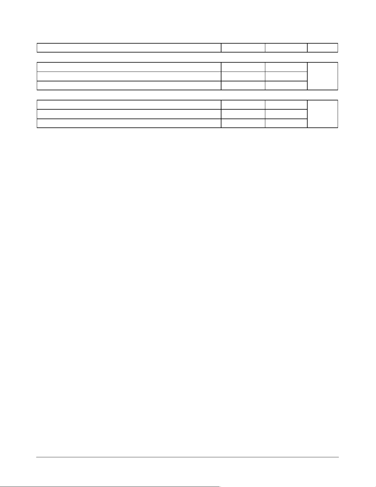
MAXIMUM RATINGS (T
Parameter
Drain-to-Source Voltage
Gate-to-Source Voltage
N-Channel
Continuous Drain
Current (Note 1)
P-Channel
Continuous Drain
Current (Note 1)
Power Dissipation
(Note 1)
N-Channel
Continuous Drain
Current (Note 2)
P-Channel
Continuous Drain
Current (Note 2)
Power Dissipation
(Note 2)
Pulsed Drain Current
Operating Junction and Storage Temperature TJ, T
Lead Temperature for Soldering Purposes
(1/8″ from case for 10 s)
Stresses exceeding Maximum Ratings may damage the device. Maximum
Ratings are stress ratings only. Functional operation above the Recommended
Operating Conditions is not implied. Extended exposure to stresses above the
Recommended Operating Conditions may affect device reliability.
1. Surface Mounted on FR4 Board using 1 in sq pad size (Cu area = 1.127 in sq
[2 oz] including traces).
2. Surface Mounted on FR4 Board using the minimum recommended pad size
of 30 mm
2
, 2 oz Cu.
= 25°C unless otherwise noted)
J
Symbol Value Unit
N-Ch
P-Ch -20
N-Ch
P-Ch
T
Steady
State
t ≤ 5 s T
Steady
State
t ≤ 5 s T
Steady
State
t ≤ 5 s 2.3
Steady
State
Steady
State
Steady
State
N-Ch
P-Ch -20
= 25°C
A
T
= 85°C 2.8
A
= 25°C 4.6
A
T
= 25°C
A
T
= 85°C -2.4
A
= 25°C -4.1
A
T
= 25°C
A
T
= 25°C
A
T
= 85°C 1.9
A
T
= 25°C
A
T
= 85°C -1.6
A
T
= 25°C
A
t
= 10 ms
p
V
V
I
DSS
GS
I
D
I
D
P
I
D
I
D
P
DM
T
D
D
STG
L
±8.0 V
-3.3
-2.3
0.71 W
-55 to
150
260 °C
20
3.8
1.5
2.6
18
V
A
A
W
A
A
A
°C
http://onsemi.com
(BR)DSS
N-Channel
20 V
P-Channel
-20 V
D2
Pin 1
MAX
DS(on)
65 mW @ 4.5 V
85 mW @ 2.5 V
120 mW @ 1.8 V
100 mW @ -4.5 V
135 mW @ -2.5 V
200 mW @ -1.8 V
D1
WDFN6
CASE 506AN
JD = Specific Device Code
M = Date Code
G = Pb-Free Package
(Note: Microdot may be in either location)
ID MAXV
3.8 A
2.0 A
1.7 A
-4.1 A
-2.0 A
-1.6 A
MARKING
DIAGRAM
1
JDMG
2
G
3
R
PIN CONNECTIONS
S1
G1
D2
1
D1
2
D2
3
(Top View)
D1
6
G2
5
4
S2
ORDERING INFORMATION
Device Package Shipping
NTLJD3119CTAG WDFN6
(Pb-Free)
NTLJD3119CTBG WDFN6
(Pb-Free)
†For information on tape and reel specifications,
including part orientation and tape sizes, please
refer to our Tape and Reel Packaging Specification
Brochure, BRD8011/D.
3000/Tape & Reel
3000/Tape & Reel
†
6
5
4
© Semiconductor Components Industries, LLC, 2007
August, 2007 - Rev. 2
1 Publication Order Number:
NTLJD3119C/D
Page 2
NTLJD3119C
THERMAL RESISTANCE RATINGS
Parameter Symbol Max Unit
SINGLE OPERATION (SELF-HEATED)
Junction-to-Ambient – Steady State (Note 3)
Junction-to-Ambient – Steady State Min Pad (Note 4)
Junction-to-Ambient – t ≤ 5 s (Note 3)
DUAL OPERATION (EQUALLY HEATED)
Junction-to-Ambient – Steady State (Note 3)
Junction-to-Ambient – Steady State Min Pad (Note 4)
Junction-to-Ambient – t ≤ 5 s (Note 3)
3. Surface Mounted on FR4 Board using 1 in sq pad size (Cu area = 1.127 in sq [2 oz] including traces).
4. Surface Mounted on FR4 Board using the minimum recommended pad size (30 mm
R
R
R
R
R
R
2
, 2 oz Cu).
q
JA
q
JA
q
JA
q
JA
q
JA
q
JA
83
177
54
58
133
40
°C/W
°C/W
http://onsemi.com
2
Page 3
NTLJD3119C
ELECTRICAL CHARACTERISTICS (T
Parameter
= 25°C unless otherwise noted)
J
Symbol N/P Test Conditions Min Typ Max Unit
OFF CHARACTERISTICS
Drain-to-Source Breakdown Voltage
Drain-to-Source Breakdown Voltage
Temperature Coefficient
Zero Gate Voltage Drain Current I
Gate-to-Source Leakage Current I
V
(BR)DSS
V
(BR)DSS/TJ
DSS
GSS
ON CHARACTERISTICS (Note 5)
Gate Threshold Voltage
Gate Threshold Temperature
Coefficient
Drain-to-Source On Resistance R
Forward Transconductance g
V
GS(TH)
V
GS(TH)/TJ
DS(on)
FS
CHARGES, CAPACITANCES AND GATE RESISTANCE
Input Capacitance
Output Capacitance C
Reverse Transfer Capacitance C
Total Gate Charge Q
Threshold Gate Charge Q
Gate-to-Source Charge Q
Gate-to-Drain Charge Q
C
ISS
OSS
RSS
G(TOT)
G(TH)
GS
GD
N
P
VGS = 0 V
ID = 250 mA
ID = -250 mA
20
-20
N 10.4
V
mV/°C
P 9.95
N VGS = 0 V, VDS = 16 V
P VGS = 0 V, VDS = -16 V -1.0
TJ = 25 °C
N VGS = 0 V, VDS = 16 V
P VGS = 0 V, VDS = -16 V -10
TJ = 85 °C
N VDS = 0 V, VGS = ±8.0 V ±100
1.0 mA
10
nA
P VDS = 0 V, VGS = ±8.0 V ±100
N
VGS = V
P
DS
ID = 250 mA
ID = -250 mA
0.4 0.7 1.0
-0.4 -0.7 -1.0
N -3.0
V
mV/°C
P 2.44
N VGS = 4.5 V , ID = 3.8 A 37 65 mW
P VGS = -4.5 V , ID = -4.1 A 75 100
N VGS = 2.5 V , ID = 2.0 A 46 85
P VGS = -2.5 V, ID = -2.0 A 101 135
N VGS = 1.8 V , ID = 1.7 A 65 120
P VGS = -1.8 V, ID = -1.6 A 150 200
N VDS = 10 V, ID = 1.7 A 4.2
S
P VDS = -5.0 V , ID = -2.0 A 3.1
N
VDS = 10 V 271
pF
P VDS = -10 V 531
N VDS = 10 V 72
f = 1.0 MHz, VGS = 0 V
P VDS = -10 V 91
N VDS = 10 V 43
P VDS = -10 V 56
N VGS = 4.5 V, VDS = 10 V, ID = 3.8 A 3.7
nC
P VGS = -4.5 V, VDS = -10 V, ID = -2.0 A 5.5
N VGS = 4.5 V, VDS = 10 V, ID = 3.8 A 0.3
P VGS = -4.5 V, VDS = -10 V, ID = -2.0 A 0.7
N VGS = 4.5 V, VDS = 10 V, ID = 3.8 A 0.6
P VGS = -4.5 V, VDS = -10 V, ID = -2.0 A 1.0
N VGS = 4.5 V, VDS = 10 V, ID = 3.8 A 1.0
P VGS = -4.5 V, VDS = -10 V, ID = -.02 A 1.4
http://onsemi.com
3
Page 4

NTLJD3119C
ELECTRICAL CHARACTERISTICS (T
= 25°C unless otherwise noted)
J
Parameter UnitMaxTypMinTest ConditionsN/PSymbol
SWITCHING CHARACTERISTICS (Note 6)
Turn-On Delay Time
Rise Time t
Turn-Off Delay Time t
Fall Time t
Turn-On Delay Time t
Rise Time t
Turn-Off Delay Time t
Fall Time t
t
d(ON)
r
d(OFF)
f
d(ON)
r
d(OFF)
f
N
P
VGS = 4.5 V, VDD = 16 V,
= 1.0 A, RG = 2.0 W
I
D
VGS = -4.5 V, VDD = -10 V,
= -2.0 A, RG = 2.0 W
I
D
DRAIN-SOURCE DIODE CHARACTERISTICS
Forward Diode Voltage
V
SD
N
VGS = 0 V, TJ = 25 °C
P IS = -1.0 A -0.75 -1.0
N
VGS = 0 V, TJ = 125 °C
P IS = -1.0 A -0.64
Reverse Recovery Time t
RR
N
P IS = -1.0 A 16.2
Charge Time t
Discharge Time t
a
b
N IS = 1.0 A 6.0
P IS = -1.0 A 10.6
N IS = 1.0 A 4.2
VGS = 0 V,
/ dt = 100 A/ms
dI
S
P IS = -1.0 A 5.6
Reverse Recovery Charge Q
RR
N IS = 1.0 A 3.0
P
5. Pulse Test: pulse width v 300 ms, duty cycle v 2%.
6. Switching characteristics are independent of operating junction temperatures.
3.8
4.7
11.1
5.8
5.2
13.2
13.7
19.1
IS = 1.0 A 0.69 1.0
IS = 1.0 A 0.52
IS = 1.0 A 10.2
IS = -1.0 A
5.7
ns
V
ns
nC
http://onsemi.com
4
Page 5

NTLJD3119C
TYPICAL PERFORMANCE CURVES - N-CHANNEL (T
10
8
6
4
2
, DRAIN CURRENT (AMPS)
D
I
0
0 0.5 21
0.1
0.09
0.08
VGS = 4 V to 2.2 V
, DRAIN-TO-SOURCE VOLTAGE (V)
V
DS
Figure 1. On-Region Characteristics Figure 2. Transfer Characteristics
TJ = 25°C
1.5 2.5 3.5
TJ = 25°C
I
= 3.8 A
D
2.0 V
1.8 V
1.6 V
1.4 V
1.2 V
10
VDS ≥ 10 V
8
6
4
TJ = 100°C
, DRAIN CURRENT (AMPS)
2
D
I
0
4
13
0.14
TJ = 25°C
0.12
0.1
= 25°C unless otherwise noted)
J
TJ = 25°C
TJ = -55°C
1.5
, GATE-TO-SOURCE VOLTAGE (V)
V
GS
2
VGS = 1.8 V
2.5
0.07
0.06
0.05
0.04
, DRAIN-TO-SOURCE RESISTANCE (W)
0.03
DS(on)
R
1.0
VGS, GATE-TO-SOURCE VOLTAGE (V)
4.03.0
Figure 3. On-Resistance versus Drain Current
1.5
ID = 3.8 A
1.4
V
= 4.5 V
GS
1.3
1.2
1.1
1.0
(NORMALIZED)
0.9
0.8
, DRAIN-TO-SOURCE RESISTANCE
0.7
DS(on)
-50 50250-25 75 125100
R
TJ, JUNCTION TEMPERATURE (°C)
Figure 5. On-Resistance Variation with
Temperature
0.08
0.06
VGS = 2.5 V
0.04
VGS = 4.5 V
0.02
, DRAIN-TO-SOURCE RESISTANCE (W)
0
DS(on)
R
1
5.02.0
6.0
32
410
56789
ID, DRAIN CURRENT (A)
Figure 4. On-Resistance versus Drain Current
and Gate Voltage
10000
1000
, LEAKAGE (nA)
DSS
I
150
100
VGS = 0 V
212104
TJ = 150°C
TJ = 100°C
6 8 14 16 18
VDS, DRAIN-TO-SOURCE VOLTAGE (V)
20
Figure 6. Drain-to-Source Leakage Current
versus Voltage
http://onsemi.com
5
Page 6

NTLJD3119C
TYPICAL PERFORMANCE CURVES - N-CHANNEL (T
600
500
400
300
200
C, CAPACITANCE (pF)
100
0
10
GATE-TO-SOURCE OR DRAIN-TO-SOURCE VOLTAGE (V)
100
VDS = 0 V
C
iss
C
rss
5 5 15 20
VGS = 0 V
C
oss
010
V
GS
V
DS
Figure 7. Capacitance Variation
VDD = 16 V
I
= 1.0 A
D
= 4.5 V
V
GS
t
d(off)
TJ = 25°C
= 25°C unless otherwise noted)
J
5
QT
4
3
V
DS
Q
GS
2
Q
GD
V
GS
1
, GATE-TO-SOURCE VOLTAGE (VOLTS)
GS
V
0
0
123
ID = 3.8 A
T
QG, TOTAL GATE CHARGE (nC)
Figure 8. Gate-To-Source and Drain-To-Source
Voltage versus Total Charge
2
VGS = 0 V
TJ = 25°C
1.5
= 25°C
J
V
20
DS
, DRAIN-TO-SOURCE VOLTAGE (VOLTS)
16
12
8
4
0
4
t
f
10
t, TIME (ns)
1
1 10 100
RG, GATE RESISTANCE (W)
Figure 9. Resistive Switching Time
Variation versus Gate Resistance
t
r
t
d(on)
1
0.5
, SOURCE CURRENT (AMPS)
S
I
0
0.4
0.6
, SOURCE-TO-DRAIN VOLTAGE (V)
V
SD
0.80.70.5
Figure 10. Diode Forward Voltage versus Current
0.9
http://onsemi.com
6
Page 7

NTLJD3119C
TYPICAL PERFORMANCE CURVES - P-CHANNEL (T
5
4.5
4
3.5
3
2.5
2
1.5
, DRAIN CURRENT (AMPS)
1
D
-I
0.5
0
0 4.521
-V
, DRAIN-TO-SOURCE VOLTAGE (V)
DS
Figure 11. On-Region Characteristics Figure 12. Transfer Characteristics
0.1
VGS = -4.5 V
0.09
0.08
0.07
VGS = -1.9 V to -6 V
3
2.51.50.5
TJ = 100°C
TJ = 25°C
TJ = 25°C
3.5
-1.8 V
-1.7 V
-1.6 V
-1.5 V
-1.4 V
-1.3 V
-1.2 V
4
= 25°C unless otherwise noted)
J
5
VDS ≥ 10 V
4
3
2
TJ = 25°C
, DRAIN CURRENT (AMPS)
1
D
-I
TJ = 125°C
0
0
-V
1
, GATE-TO-SOURCE VOLTAGE (V)
GS
0.15
TJ = 25°C
0.1
TJ = -55°C
1.5
VGS = -2.5 V
VGS = -4.5 V
20.5
2.5
3
0.06
0.05
, DRAIN-TO-SOURCE RESISTANCE (W)
0.04
DS(on)
1.0 2.01.5
R
TJ = -55°C
-ID, DRAIN CURRENT (A)
Figure 13. On-Resistance versus Drain
Current
1.6
ID = -2.2 A
V
= -4.5 V
GS
1.4
1.2
1.0
(NORMALIZED)
0.8
, DRAIN-TO-SOURCE RESISTANCE
0.6
DS(on)
-50 50250-25 75 125100
R
TJ, JUNCTION TEMPERATURE (°C)
Figure 15. On-Resistance Variation with
Temperature
0.05
, DRAIN-TO-SOURCE RESISTANCE (W)
2.5 3
12
R
0
DS(on)
-ID, DRAIN CURRENT (A)
Figure 14. On-Resistance versus Drain
Current and Gate Voltage
10000
1000
, LEAKAGE (nA)
DSS
-I
150
100
10
VGS = 0 V
TJ = 150°C
TJ = 100°C
212104
6 8 14 16 18
-VDS, DRAIN-TO-SOURCE VOLTAGE (V)
Figure 16. Drain-to-Source Leakage Current
versus Voltage
4
5
20
http://onsemi.com
7
Page 8

NTLJD3119C
TYPICAL PERFORMANCE CURVES - P-CHANNEL (T
1200
VDS = 0 V
1000
C
iss
800
600
400
C
rss
C, CAPACITANCE (pF)
200
0
5 5 15 20
GATE-TO-SOURCE OR DRAIN-TO-SOURCE VOLTAGE (V)
1000
VDD = -15 V
I
= -2.2 A
D
V
GS
100
VGS = 0 V
C
oss
010
V
GS
V
DS
Figure 17. Capacitance Variation
= -4.5 V
TJ = 25°C
= 25°C unless otherwise noted)
J
5
QT
4
, GATE-TO-SOURCE VOLTAGE (VOLTS)
GS
-V
3
V
DS
Q
GS
2
Q
GD
1
0
0
V
GS
43
ID = -2.2 A
T
= 25°C
J
5
QG, TOTAL GATE CHARGE (nC)
Figure 18. Gate-To-Source and Drain-To-Source
Voltage versus Total Charge
3
VGS = 0 V
2.5
2
-V
20
DS
, DRAIN-TO-SOURCE VOLTAGE (VOLTS)
16
12
8
4
0
621
t
f
t
t, TIME (ns)
10
t
d(off)
t
d(on)
r
1
1 10 100
RG, GATE RESISTANCE (W)
Figure 19. Resistive Switching Time
Variation versus Gate Resistance
100
TC = 25°C
T
= 150°C
J
SINGLE PULSE
10
1
*See Note 2 on Page 1
0.1
, DRAIN CURRENT (AMPS)
D
-I
0.01
0.1 1 100
-V
DS
Figure 21. Maximum Rated Forward Biased
1.5
1
0.5
, SOURCE CURRENT (AMPS)
s
-I
0
0
0.1 0.7 0.90.50.3
-V
SD
Figure 20. Diode Forward Voltage versus Current
10 ms
100 ms
1 ms
10 ms
R
LIMIT
DS(on)
THERMAL LIMIT
dc
PACKAGE LIMIT
10
, DRAIN-TO-SOURCE VOLTAGE (V)
Safe Operating Area
TJ = 150°C
0.6
TJ = 25°C
0.80.40.2
, SOURCE-TO-DRAIN VOLTAGE (V)
1.0
http://onsemi.com
8
Page 9

NTLJD3119C
1000
100
0.1
EFFECTIVE TRANSIENT THERMAL RESISTANCE
10
1
D = 0.5
0.2
0.1
0.05
0.02
0.01
TYPICAL PERFORMANCE CURVES (T
P
SINGLE PULSE
t, TIME (s)
Figure 22. Thermal Response
= 25°C unless otherwise noted)
J
(pk)
t
1
t
2
DUTY CYCLE, D = t1/t
10.010.00001
*See Note 2 on Page 1
D CURVES APPLY FOR POWER
PULSE TRAIN SHOWN
READ TIME AT t
T
- TA = P
J(pk)
2
(pk)
1
R
(t)
q
JA
100 1000100.10.0010.00010.000001
http://onsemi.com
9
Page 10

NTLJD3119C
PACKAGE DIMENSIONS
WDFN6, 2x2
CASE 506AN-01
ISSUE B
NOTES:
1. DIMENSIONING AND TOLERANCING PER
ASME Y14.5M, 1994.
2. CONTROLLING DIMENSION: MILLIMETERS.
3. DIMENSION b APPLIES TO PLATED
TERMINAL AND IS MEASURED BETWEEN
0.15 AND 0.20mm FROM TERMINAL.
4. COPLANARITY APPLIES TO THE EXPOSED
PAD AS WELL AS THE TERMINALS.
MILLIMETERS
DIMAMIN MAX
0.70 0.80
A1 0.00 0.05
A3 0.20 REF
b 0.25 0.35
D 2.00 BSC
D2 0.57 0.77
2.00 BSC
E
E2
0.90 1.10
e
0.65 BSC
0.25 REF
K
L
0.20 0.30
J
0.15 REF
2X
2X
PIN ONE
REFERENCE
0.10 C
0.10 C
0.10 C
D
A
B
E
A3
A
6X
0.08 C
6X
D2
L
1
A1
SEATING
C
D2
4X
3
e
PLANE
6X
0.43
SOLDERMASK DEFINED
MOUNTING FOOTPRINT*
2.30
6X
0.35
1
E2
2X
0.65
PITCH
6X
K
6
J6X
BOTTOM VIEW
4
b
6X
A0.10 C
B
0.05 C
NOTE 3
0.250.25
2X
0.72
1.05
DIMENSIONS: MILLIMETERS
*For additional information on our Pb-Free strategy and soldering
details, please download the ON Semiconductor Soldering and
Mounting Techniques Reference Manual, SOLDERRM/D.
ON Semiconductor and are registered trademarks of Semiconductor Components Industries, LLC (SCILLC). SCILLC reserves the right to make changes without further notice
to any products herein. SCILLC makes no warranty, representation or guarantee regarding the suitability of its products for any particular purpose, nor does SCILLC assume any liability
arising out of the application or use of any product or circuit, and specifically disclaims any and all liability, including without limitation special, consequential or incidental damages.
“Typical” parameters which may be provided in SCILLC data sheets and/or specifications can and do vary in different applications and actual performance may vary over time. All
operating parameters, including “Typicals” must be validated for each customer application by customer's technical experts. SCILLC does not convey any license under its patent rights
nor the rights of others. SCILLC products are not designed, intended, or authorized for use as components in systems intended for surgical implant into the body, or other applications
intended to support or sustain life, or for any other application in which the failure of the SCILLC product could create a situation where personal injury or death may occur. Should
Buyer purchase or use SCILLC products for any such unintended or unauthorized application, Buyer shall indemnify and hold SCILLC and its officers, employees, subsidiaries, affiliates,
and distributors harmless against all claims, costs, damages, and expenses, and reasonable attorney fees arising out of, directly or indirectly, any claim of personal injury or death
associated with such unintended or unauthorized use, even if such claim alleges that SCILLC was negligent regarding the design or manufacture of the part. SCILLC is an Equal
Opportunity/Affirmative Action Employer. This literature is subject to all applicable copyright laws and is not for resale in any manner.
PUBLICATION ORDERING INFORMATION
LITERATURE FULFILLMENT:
Literature Distribution Center for ON Semiconductor
P.O. Box 5163, Denver, Colorado 80217 USA
Phone: 303-675-2175 or 800-344-3860 Toll Free USA/Canada
Fax: 303-675-2176 or 800-344-3867 Toll Free USA/Canada
Email: orderlit@onsemi.com
N. American Technical Support: 800-282-9855 Toll Free
USA/Canada
Europe, Middle East and Africa Technical Support:
Phone: 421 33 790 2910
Japan Customer Focus Center
Phone: 81-3-5773-3850
ON Semiconductor Website: www.onsemi.com
Order Literature: http://www.onsemi.com/orderlit
For additional information, please contact your local
Sales Representative
http://onsemi.com
10
NTLJD3119C/D
 Loading...