

Page 1

NTE990
Integrated Circuit
Dual Audio Power Amplifier
Description:
The NTE990 is a monolithic dual power amplifier designed to deliver 2W/channel continuous into 8Ω
loads. The NTE990 is designed to operate with a low number of external components, and still provide flexibility for use in stereo phonographs, tape records and AM–FM stereo receivers, etc. Each
power amplifier is biased from a common internal regulator to provide high power supply rejection,
and output Q point centering. The NTE990 is internally compensated for all gains greater than 10.
Features:
D 2W/channel
D –65 dB Ripple Rejection, Output Referred
D –65 dB Channel Separation, Output Referred
D Wide Supply Range: 6V to 24V
D Very Low Cross–Over Distortion
D Low Audio Band Noise
D AC Short Circuit Protected
D Internal Thermal Shutdown
Applications:
D Multi–Channel Audio Systems
D Stereo Phonographs
D Tape Recorders and Players
D AM–FM Radio Receivers
D Servo Amplifiers
D Intercom Systems
D Automotive Products
Absolute Maximum Ratings:
Supply Voltage, V
Input Voltage, V
Operating Junction Temperature, T
Operating Temperature Range, T
Storage Temperature Range, T
CC
I
J
opr
stg
Lead Temperature (During Soldering, 10sec), T
26V. . . . . . . . . . . . . . . . . . . . . . . . . . . . . . . . . . . . . . . . . . . . . . . . . . . . . . . . . . . . . . . .
±0.7V. . . . . . . . . . . . . . . . . . . . . . . . . . . . . . . . . . . . . . . . . . . . . . . . . . . . . . . . . . . . . . . . .
+150°C. . . . . . . . . . . . . . . . . . . . . . . . . . . . . . . . . . . . . . . . . . . . . . .
0° to +70°C. . . . . . . . . . . . . . . . . . . . . . . . . . . . . . . . . . . . . . . . . . .
–65° to +150°C. . . . . . . . . . . . . . . . . . . . . . . . . . . . . . . . . . . . . . . . . .
L
+300°C. . . . . . . . . . . . . . . . . . . . . . . . . . . . . . . . . . . .
Page 2
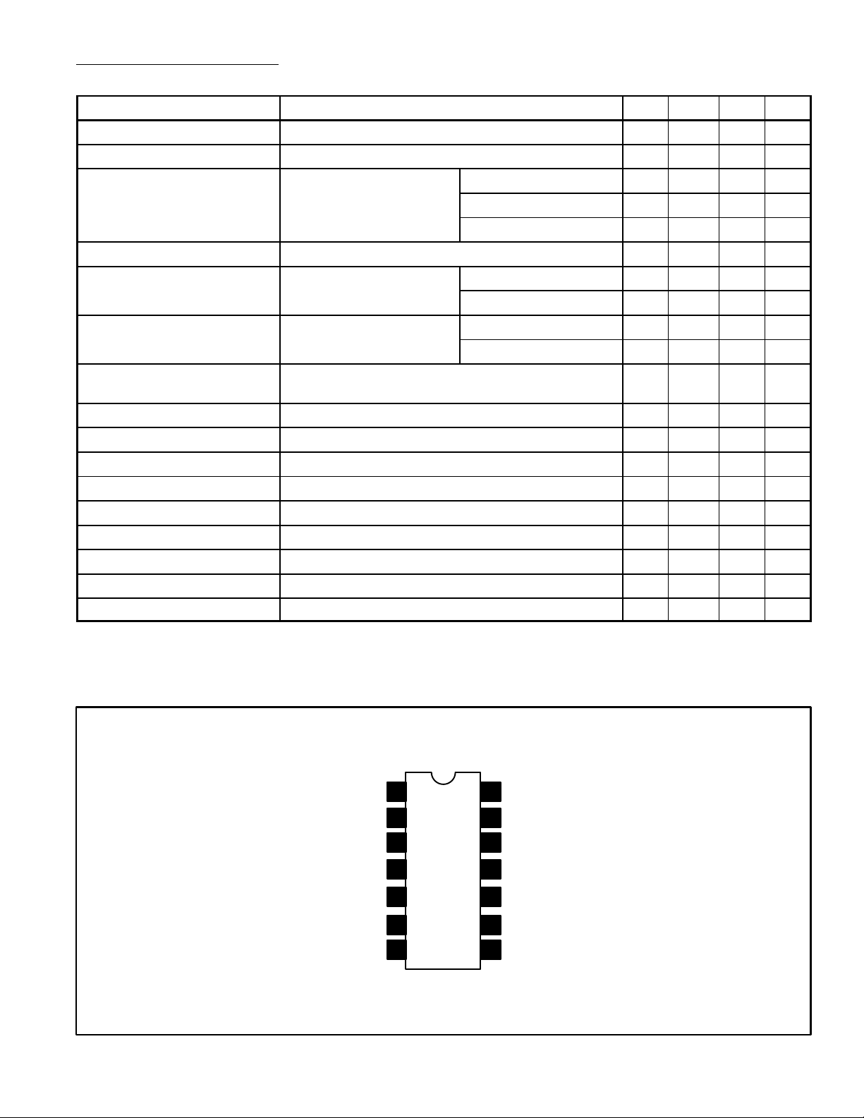
Electrical Characteristics: (VS = 20V, TA = +25°C, RL = 8Ω, AV = 50 (34 dB) unless otherwise
specified)
Parameter Test Conditions Min Typ Max Unit
Total Supply Current PO= 0W – 25 50 mA
Output Power THD = 10% 2.0 – – W/Ch
Total Harmonic Distortion f = 1kHz, VS = 14V PO = 50mW/Ch – 0.075 – %
PO = 500mW/Ch – 0.045 – %
PO = 1W/Ch – 0.055 – %
Output Swing RL = 8Ω – VS –6 – V
Channel Separation
CF = 50µF, CIN = 0.1µF,
f = 1kHz, Output Referred
Power Supply Rejection Ratio
CF = 50µF, CIN = 0.1µF,
f = 120Hz, Output Referred
Equivalent Noise Input RS = 0, CIN = 0.1µF, BW = 20Hz to 20kHz,
VS = 20V, VO = 4V
VS = 7V, VO = 0.5V
VS = 20V, V
VS = 7V, V
ripple
ripple
= 1V
= 0.5V
rms
rms
–50 –70 – dB
– –60 – dB
–50 –65 – dB
rms
rms
– –40 – dB
– 2.5 – µA
P–P
Output Noise Wideband
RS = 0, CIN = 0.1µF, AV = 200 – 0.8 – mV
Open Loop Gain RS = 0, f = 100kHz, RL = 8Ω – 70 – dB
Input Offset Voltage – 15 – mV
Input Bias Current – 50 – nA
Input Impedance Open Loop – 4 – MΩ
DC Output Level VS = 20V 9 10 11 V
Slew Rate – 2.0 – V/µs
Power Bandwidth – 65 – kHz
Current Limit – 1.0 – A
Note 1 For operation at ambient temperature greater than +25°C, the NTE990 must be derated
based on a maximum 150°C junction temperature using a thermal resistance which depends upon device mounting techniques..
Pin Connection Diagram
Bias
Output 1
GND
GND
GND
Input 1
Feedback 1
1
2
3
4
5
6
7
V
14
Output 2
13
GND
12
GND
11
10
GND
Input 2
9
Feedback 2
8
CC
Page 3

14 8
17
.785 (19.95)
Max
.200 (5.08)
Max
.100 (2.45) .099 (2.5) Min
.600 (15.24)
.300
(7.62)
 Loading...