

Page 1

NTE976
Integrated Circuit
Operational Amplifier
Description:
The NTE976 is a general purpose operational amplifier with the necessary frequency compensation
built into a single 8–Lead DIP type package. Advanced processing techniques make the input currents a factor of ten lower than industry standards like the NTE909. Yet, it is a direct plug–in replacement for the NTE909 and the NTE941M.
This device provides better accuracy and lower noise in high impedance circuitry. The low input currents also make it particularly well suited for long interval integrators or timers, sample and hold circuits, and low frequency waveform generators. Further, replacing circuits where matched transistor
pairs buf fer the inputs of conventional IC op amps, the NTE976 can give lower of fset voltage and drift
at a lower cost.
Features:
D Offset Voltage over Temperature: 3mV Max
D Input Current over Temperature: 100nA Max
D Offset Current over Temperature: 20nA Max
D Guaranteed Drift Characteristics
Absolute Maximum Ratings:
Supply Voltage,
V
CC
V
EE
Power Dissipation (Note 1), P
Differential Input Voltage, V
Input Voltage (Note 2), V
Output Short–Circuit Duration, t
Operating Temperature Range, T
Storage Temperature Range, T
D
ID
IN
s
A
stg
Lead Temperature (During Soldering, 10sec), T
0° to +70°C. . . . . . . . . . . . . . . . . . . . . . . . . . . . . . . . . . . . . . . . . . . . .
–65° to +150°C. . . . . . . . . . . . . . . . . . . . . . . . . . . . . . . . . . . . . . . . . .
L
+18V. . . . . . . . . . . . . . . . . . . . . . . . . . . . . . . . . . . . . . . . . . . . . . . . . . . . . . . . . . . . . . . . . . . . . . .
–18V. . . . . . . . . . . . . . . . . . . . . . . . . . . . . . . . . . . . . . . . . . . . . . . . . . . . . . . . . . . . . . . . . . . . . . . .
500mW. . . . . . . . . . . . . . . . . . . . . . . . . . . . . . . . . . . . . . . . . . . . . . . . . . .
±30V. . . . . . . . . . . . . . . . . . . . . . . . . . . . . . . . . . . . . . . . . . . . . . . . . . . . . . .
15V. . . . . . . . . . . . . . . . . . . . . . . . . . . . . . . . . . . . . . . . . . . . . . . . . . . . . . . . .
Indefinite. . . . . . . . . . . . . . . . . . . . . . . . . . . . . . . . . . . . . . . . . . . . . . . .
+300°C. . . . . . . . . . . . . . . . . . . . . . . . . . . . . . . . . . . .
Note 1. The ma ximu m jun ctio n temp era ture o f the NT E976 i s +10 0°C. The thermal resistance
junction to ambient is +100°C/W.
Note 2. For supply voltages less than –15V, the absolute maximum input voltage is equal to the
supply voltage.
Page 2
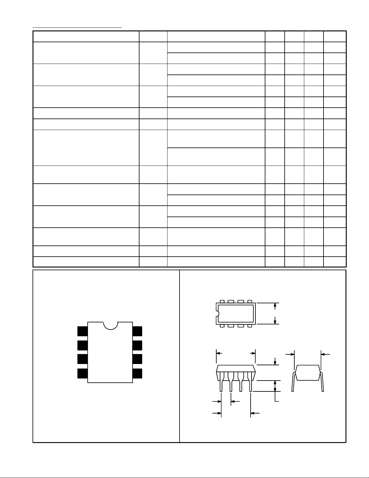
Electrical Characteristics: (0° ≤ TA ≤ +70°C, ±5V ≤ VS ≤ ±15V unless otherwise specified)
Parameter Symbol Test Conditions Min Typ Max Unit
Input Offset Voltage V
Input Offset Current I
Input Bias Current I
Input Resistance r
Supply Current I
Large Signal Voltage Gain A
Average Temperature Coefficient
TCV
of Input Offset Voltage
Average Temperature Coefficient
TCI
of Input Offset Current
Output Voltage Swing V
IO
IB
TA = +25°C, RS ≤ 50kΩ – 2.0 7.5 mV
IO
RS ≤ 50kΩ – – 10 mV
TA = +25°C – 3.0 50 nA
– – 70 nA
TA = +25°C – 70 250 nA
– – 300 nA
TA = +25°C 0.5 2.0 – MΩ
i
TA = +25°C, VS = ±15V – 1.8 3.0 mA
D
TA = +25°C, VS = ±15V,
v
IO
IO
= ±10V, RL ≥ 2kΩ
V
OUT
VS = ±15V, V
≥ 2kΩ
R
L
OUT
= ±10V,
+25°C ≤ TA ≤ +70°C – 0.01 0.3 nA/°C
25 160 – V/mV
15 – – V/mV
– 6.0 30 µV/°C
0°C ≤ TA ≤ +25°C – 0.02 0.6 nA/°C
VS = ±15V, RL = 10kΩ ±12 ±14 – V
O
VS = ±15V, RL = 2kΩ ±10 ±13 – V
Input Voltage Range V
ICR
VS = ±15V ±12 +15
– V
–13
Common Mode Rejection Ratio CMRR RS ≤ 50kΩ 70 90 – dB
Supply Voltage Rejection Ratio PSRR RS ≤ 50kΩ 70 96 – dB
Pin Connection Diagram
85
.256 (6.52) Max
N.C.
Inverting Input12
Non–Inverting
Input
V (–)
8
N.C.
V (+)
7
3
4
Output
6
5 N.C.
14
.393 (10.0)
Max
.150
(3.81)
.300 (7.62)
.070 (1.77) Min.100 (2.54)
.300 (7.62)
 Loading...