

3.3 - 119
3.3
OM3914NKM
1 08 R2
Supersedes 4 11 R1
OM3914STM
OM3914NTM
Three Terminal, Negative Adjustable
Voltage Regulator In Hermetic
Packages
3 AMP NEGATIVE ADJUSTABLE REGULATOR APPROVED
TO DESC DRAWING 5962-87741
FEATURES
• Similar To Industry Standard LT1033
• Approved To DESC Standardized Military Drawing Number 5962-8774101
• Adjustable Output Voltage
• Built In Thermal Overload Protection
• Short Circuit Current Limiting
• Maximum Output Voltage Tolerance is Guaranteed To ±1%
• Guaranteed Dropout Voltage At Multiple Current Levels
• TO-257 Available in Isolated and Non-Isolated Packages
DESCRIPTION
This three terminal negative adjustable voltage regulator is designed to provide 3A
with higher efficiency than conventional voltage regulators. This device is designed
to operate down to 1 Volt input to output differential and the dropout voltage is fully
specified as a function of load current. Supplied in easy-to-use hermetic TO-257 and
TO-3, this device is ideally suited for Military applications where small size and high
reliability is required.
ABSOLUTE MAXIMUM RATINGS @ 25°C
Power Dissipation (Pd) . . . . . . . . . . . . . . . . . . . . . . . . . . . . . . . . . . . Internally Limited
Input - Output Voltage Differential . . . . . . . . . . . . . . . . . . . . . . . . . . . . . . . . . . . . 35 V
Operating Junction Temperature Range . . . . . . . . . . . . . . . . . . . . . - 55°C to + 150°C
Storage Temperature Range . . . . . . . . . . . . . . . . . . . . . . . . . . . . . . - 65°C to + 150°C
Lead Temperature (Soldering 10 seconds) . . . . . . . . . . . . . . . . . . . . . . . . . . . . 300°C
Thermal Resistance Junction to Case:
(TO-257, Isolated) . . . . . . . . . . . . . . . . . . . . . . . . . . . . . . . . . . . . . . . . 3.5°C/W
(TO-257, Non-Isolated) . . . . . . . . . . . . . . . . . . . . . . . . . . . . . . . . . . . . . 2.3°C/W
(TO-3) . . . . . . . . . . . . . . . . . . . . . . . . . . . . . . . . . . . . . . . . . . . . . . . . . . 3.0°C/W
Recommended Operating Conditions:
Output Voltage Range . . . . . . . . . . . . . . . . . . . . . . . . . . . . . . . . . . . . . -3V to -15 V
Ambient Operating Temperature Range (TA) . . . . . . . . . . . . . . . . - 55°C to + 125°C
Input Voltage Range . . . . . . . . . . . . . . . . . . . . . . . . . . . . . . . . . . . . . . . - 5V to -35 V
3.3 - 120
3.3
OM3914STM OM3914NTM OM3914NKM
ELECTRICAL CHARACTERISTICS -55°C ≤ T
A
≤ +125°C (unless otherwise specified)
Parameter Symbol Test Conditions Min. Max. Unit
Reference Voltage V
REFVIN
- V
OUT
= 5 V, I
OUT
= 5 mA, TA= 25° C -1.238 -1.262
V
3 V ≤V
IN
- V
OUT
≤35 V • -1.215 -1.285
Line Regulation ∆V
OUT
3 V ≤VIN- V
OUT
≤35 V
0.015
%/V
(Note 1) ∆V
IN
• 0.04
Load Regulation ∆V
OUT
V
OUT
≤5 V, TA= 25° C 50
mV
(Note 1) ∆I
OUT
10 mA ≤ I
OUT
≤ I
MAX.
• 75
V
OUT
≥ 5.0 V 1.0
%
10 mA ≤ I
OUT
≤ I
MAX.
• 1.5
Thermal Regulation - 30 ms pulse, T
A
= 25° C 0.02 %/W
Ripple Rejection ∆V
IN
V
OUT
= -10 V, f = 120 Hz, C
Adj
= 0
56
dB
(Note 2) ∆V
REF
• 53
V
OUT
= -10 V, f = 120 Hz, C
Adj
= 10 µF
70
dB
• 60
Adjust Pin Current I
Adj
V
DIFF
= 35 V, IL= 10 mA • 100 µA
Adjust Pin Current Change ∆I
Adj
10 mA ≤ I
OUT
≤ I
MAX.
• 2.0
µA
3 V ≤V
IN
- V
OUT
≤35 V • 5.0
Minimum Load Current I
Min
VIN- V
OUT
≤35 V • 5.0
mA
V
IN
- V
OUT
≤10 V • 3.0
Current Limit I
Lim
VIN- V
OUT
≤10 V
3.0 6.0
A
• 3.0
V
IN
- V
OUT
= 35 V
0.5 2.5
A
• 0.5
Temperature Stability ∆V
OUT
-55° C ≤ TJ≤ +125° C
•
1.5 %
(Note 2) ∆T
Long Term Stability ∆V
OUT
TA= +125° C, t = 1000 hrs 1.0 %
(Note 2) ∆T
Notes:
1. Line and Load Regulation are measured at a constant junction temperature using a low duty cycle pulse technique.
Although power dissipation is internally limited, regulation is guaranteed up to the maximum power dissipation of 30 W.
Power dissipation is determined by the input/output differential voltage and the output current. Guaranteed maximum
power dissipation will not be available over the full input/output voltage range.
2. Guaranteed by design, characterization or correlation to other tested parameters.
3. The • denotes the specifications which apply over the full operating temperature range.
Part Numbering System
Voltage Regulators
OM-3914-S-T-M
Company
Identification
Part
Number
S= Isolated
N= Non isolated
Package
(see Package codes*)
Screening
M= MIL-M 38535
PART NUMBER DESIGNATOR
Standard Military Drawing Number Omnirel Part Number
5962-8774101U OM3914STM
5962-8774101T OM3914NTM
5962-8774101X OM3914NKM
“U” = Isolated
“T” = Non-Isolated

3.3 - 121
3.3
OM3914STM OM3914NTM OM3914NKM
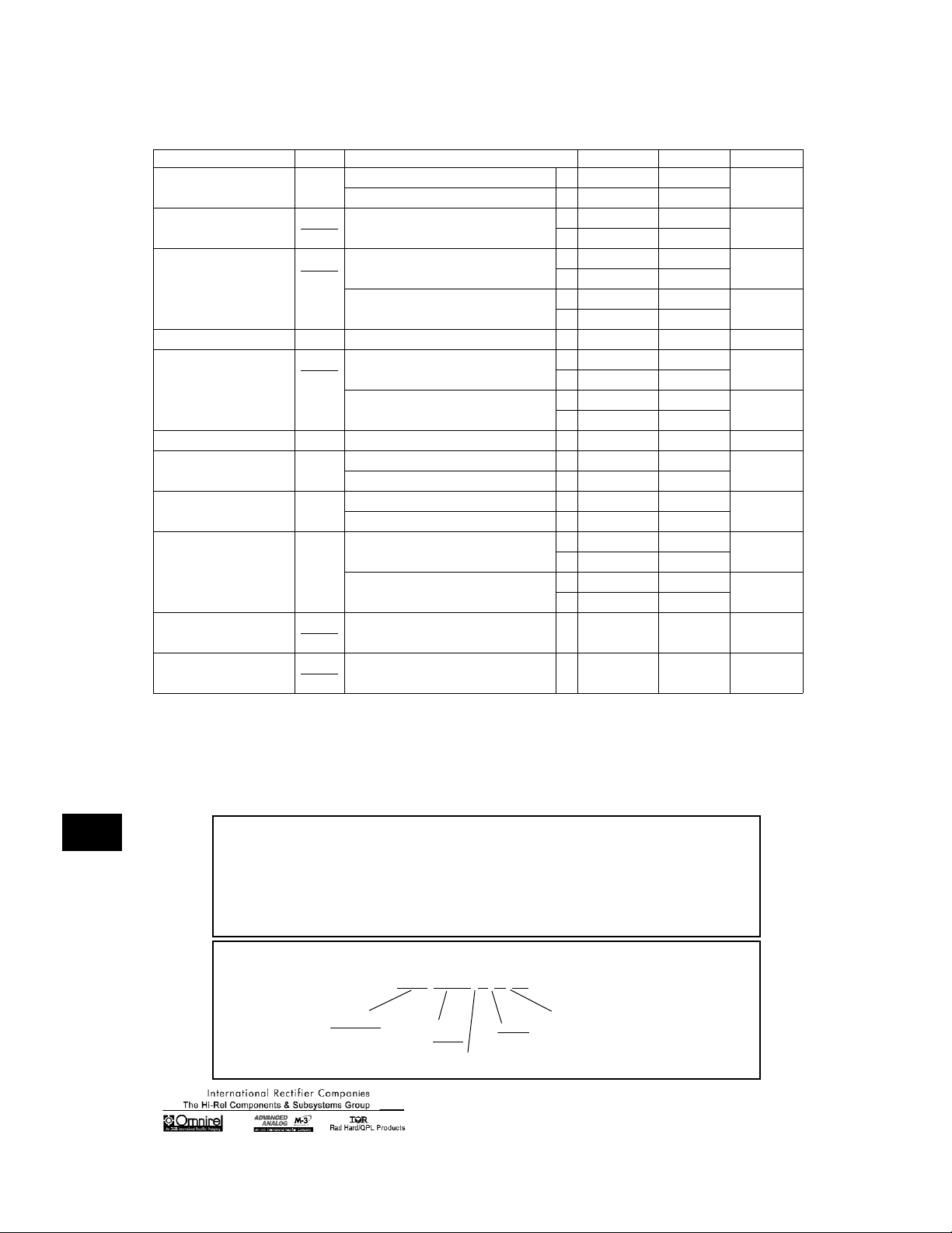
TYPICAL PERFORMANCE CHARACTERISTICS
Reference Voltage (V)
1.270
1.260
1.250
1.240
1.230
-75 -50 -25 0 25 50 75 100 125150
Temperature (°C)
Output Current (A)
5
4
3
2
1
0
0 5 10 15 20 25 30 35
Input-Output Differential (V)
Output Voltage
Deviation (%)
0.8
0.4
0
-0.4
-0.8
0 0.8 1.6 2.4 3.2 4.0
Output Current (A)
Ripple Rejection (dB)
100
80
60
40
20
0
0.01 0.1 1 10
C
ADJ
= 0
VIN = -15 V
V
OUT
= -10 V
C
ADJ
= 10µF
f = 120Hz, TJ = 25°C
Current (mA)
1.8
1.6
1.4
1.2
1.0
0.8
0.6
0.4
0.2
0
0 10203040
Input-Output Differential (V) Output Current (A)
TJ = -55°C
TJ = 25°C
TJ = 150°C
Input-Output Differential (V)
2.8
2.6
2.4
2.2
2.0
1.8
1.6
1.4
1.2
0.5 1.0 1.5 2.0 2.5 3.0
Output Current (A)
TJ = -55°C
TJ = -25°C
TJ = -150°C
DROPOUT VOLTAGE TEMPERATURE STABILITY
MINIMUM LOAD CURRENT RIPPLE REJECTION
LOAD REGULATION GUARANTEED MINIMUM
OUTPUT CURRENT

3.3
OM3914STM OM3914NTM OM3914NKM
TYPICAL APPLICATIONS
Front View
123
MECHANICAL OUTLINES
.430
.410
.200
.190
.038 MAX.
.005
.120 TYP.
.537
.527
.665
.645
.420
.410
.150
.140
.750
.500
.100 TYP.
.035
.025
.045
.035
MULTIPLE TRACKING REGULATORS
HIGH STABILITY REGULATOR
-V
OUT
-V
IN
V
IN
V
OUT
C2
+
5µF
C1
C3
+
10µF
2µF
ADJ.
OM3914
R2
R1
+
V
REF
I
ADJ
V
OUT
= V
REF
(
1+ R2 )+ I
ADJ
(R2)
R1
NOTES:
• Case is metal/hermetically sealed
• Isolated Tab
Tab
4
CASE T
Pin 1 - Adjust
Pin 2 - VIN
Pin 3 - VOUT
Tab - VIN
CASE U
Pin 1 - Adjust
Pin 2 - VIN
Pin 3 - VOUT
Tab - No Connection
1.197
1.177
0.675
0.655
0.188 R.
MAX.
0.440
0.420
0.161
0.151
0.525 R.
MAX.
0.225
0.205
SEATING
PLANE
0.312
MIN.
0.450
0.250
0.043
0.038
2 PLCS.
0.135
MAX.
0.875
MAX.
1.53
REF.
OM3914NKM
Pin 1 – Adjust
Pin 2 – Vout
Case – Vin
TO-3
+
C3
+
10µF
R2
2µF
-V
IN
V
IN
OM3914
ADJ.
R1
IN4002
V
OUT
+
C1
2µF
Solid
Tantalum
-V
OUT
1
7V
LM329B
+
5µF 2µF
R3
1.5k
1%
ADJ.
V
-V
IN
IN
OM3914
V
OUT
*R2 =
R2*
R1
1k
1%
V
OUT
9.08 X 10
+
Solid
Tantalum
-V
-3
OUT
+
2µF
ADJ.
V
R2
IN
OM3914
+
2µF
IN4002
V
OUT
ADJ.
V
V
R#N
IN
OUT
OM3914
+
2µF
Solid
Tantalum
-V
+
2µF
Solid
Tantalum
-V
OUT
OUT
2
3
 Loading...