OKI OKIPAGE 6w Repair manual

OKIPAGE6w
LED Page Printer
Troubleshooting Manual
with Component Parts List
(OEL)
All specifications are subject to change without notice.

CONTENTS
1. OUTLINE.....................................................................................................1
2. TOOLS........................................................................................................1
3. CIRCUIT DESCRIPTION............................................................................2
3.1 Outline.....................................................................................................................2
3.2 CPU and Memory....................................................................................................4
3.3 Reset Control...........................................................................................................6
3.4 EEPROM Control.....................................................................................................7
3.5 Centronics Parallel Interface....................................................................................8
3.6 Front Operator Panel...............................................................................................9
3.7 LED Head Control.................................................................................................10
3.8 Motor and clutch control........................................................................................12
3.9 Fuser Temperature Control....................................................................................14
3.10Sensor Control.......................................................................................................17
3.11Cover Open...........................................................................................................18
3.12Power Supply Part.................................................................................................19
4. TROUBLESHOOTING..............................................................................21
4.1 Troubleshooting Table............................................................................................21
4.2 Troubleshooting Flowchart.....................................................................................23
5. CIRCUIT DIAGRAM..................................................................................27
6. COMPONENT PARTS LIST AND LAYOUT.............................................. 36
6.1 HUK PCB ............................................................................................................
6.2 P2H PCB
6.3 P6L PCB
............................................................................................................
............................................................................................................
37
41
46

1. OUTLINE
This manual has been written to provide guidance for troubleshooting of the OKIPAGE6w Printer
(primarily for its printed circuit boards), on an assumption that the reader is knowledgeable of the
printer. Read the maintenance manual for this printer if necessary.
Note:
1. High voltage power supply board and power supply unit containing a high voltage power
supply is dangerous. From the viewpoint of the safety standards, the local repairing of a
defective board is not allowed. Thus, the objects to be locally repaired as a result of
troubleshooting are switches.
2. TOOLS
For troubleshooting the printer, the tools listed below may be needed in addition to general
maintenance tools.
Oscilloscope Frequency response 100 MHz or higher
Soldering iron A slender tip type, 15-20 watts
Tool Remarks
- 1 -

3. CIRCUIT DESCRIPTION
3.1 Outline
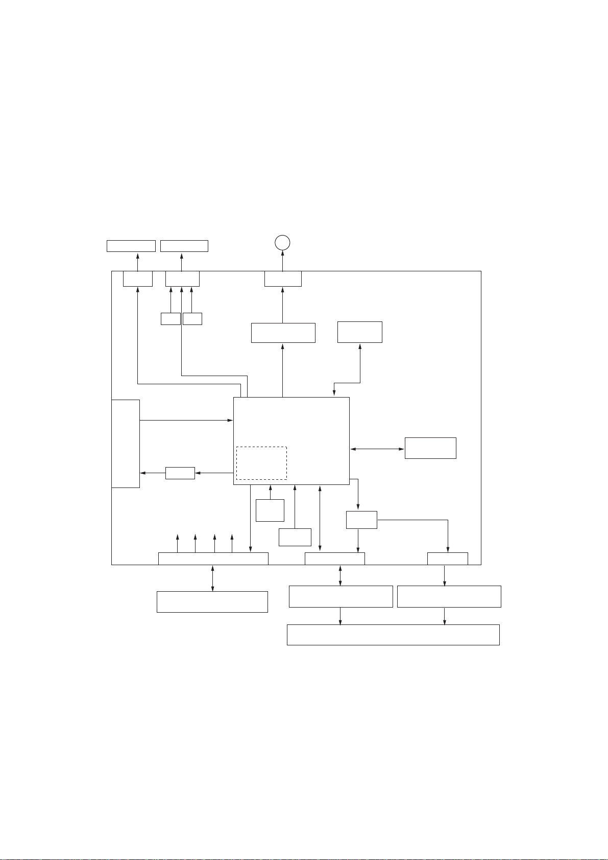
The circuit of OKIPAGE6w consists of a main control board, a main high voltage power supply
board,a syb-high voltage power supply board and a power supply unit. The block diagram is
shown in Fig. 3-1. The main control board controls the reception and transmission of data with
a host I/f and processes command analysis, bit image development, raster buffer read. It also
controls the engine and high voltage outputs.
(1)Reception and transmission control
The main control board has one parallel I/F port which is compliant to the IEEE 1284
specification.
An interface task stores all data received from the host into a receive buffer first, and returns
the printer status upon request of the host.
(2)Command analysis processing
The OKIPAGE6w printer has the following emulation mode.
Hiper-W: OKI original
An edit task fetches data from the receive buffer, analizes commands, and sets I/O registers.
(3)Raster data processing
The decompression circuit in the CPU expands the compressed data and stores the data into
the raster buffer.
(4)Raster data transfer
The LED head control circuit in the CPU sends the data stored in the raster buffer to the LED
head.
(5)High voltage control (main, sub)
The high voltage control circuit in the CPU.
The high voltage power supply board generates high voltage outputs, and have sensors, LED for
display.
The power supply unit generates +26VDC output, +5DC output.
- 2 -
Motor
Parallel
I/F
PLUNGER
CN4
LED HEAD
HEAD1CN8
0V5V
LS07
+5V+26V
Motor Driver
MTD2005F
PCB H63-ONLY
Internal
MASK ROM
62KB
OSC
16MHz
0VP0V
CN7
CPU
(nX8)
RST
EEPROM
Serial I/F
DRAM Bus
(Data : 4)
(Address : 11)
1kb
DRAM
512kB
DRAM
1M x 4
HC125
CN2
High Voltage Power Unit
Power Supply Unit
Figure 3-1 OKIPAGE6w Block Diagram
- 3 -
P2H
CN10CN1
High Voltage Power Unit
P6L
ID Unit

3.2 CPU and Memory
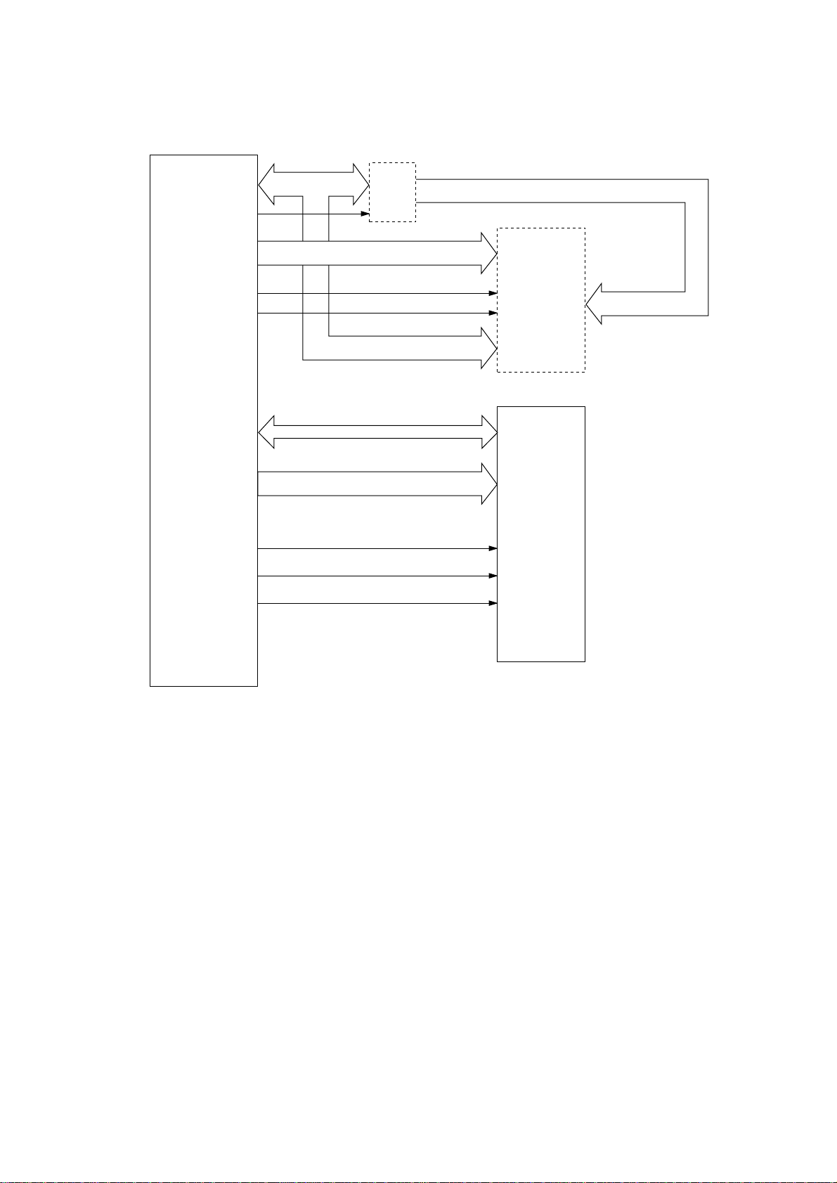
(1)CPU (MSM65917)
CPU core nX-8
CPU clock 16 MHz
Data bus width External 8 bits, Internal 8 bits
(2)Program ROM
ROM capacity 64k-bytes
ROM type 512 kbits (64k x 8 bits)
Access time 90 nsec
(3)Resident RAM
RAM capacity 512k bytes (1M x 4 bits D-RAM one piece)
RAM type 4M bits (1M x 4 bits)
Access time 60 ns
- 4 -
CPU
IC 6
ALE
RDN
ROCS
DA10
DWR
CAS
AD00 to AD07
LS373
IC3
A08 to A15
DD00 to DD03
DA00 to DA09
A00 to A07
IC2
EPROM
(64k x 8 bits)
IC11
DRAM
(1M x 4 bits)
RAS0
RAS1
RAS2
Main Control Board
Figure 3-2 Block Diagram of CPU & Memory in OKIPAGE6w
- 5 -
3.3 Reset Control
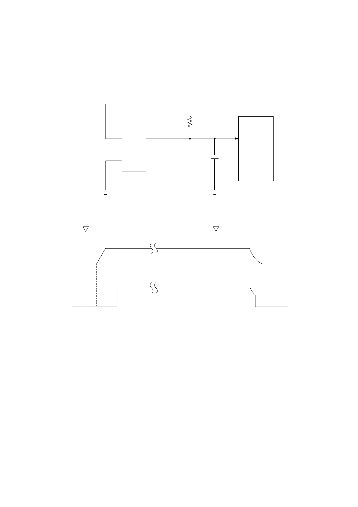
When power is turned on, RST-N signal is generated by IC5.
+5V+5V
IC6
+5V
Power ON
IC5
1
3
2
Power OFF
63
CPU
RSTN
RST-N
- 6 -
3.4 EEPROM Control
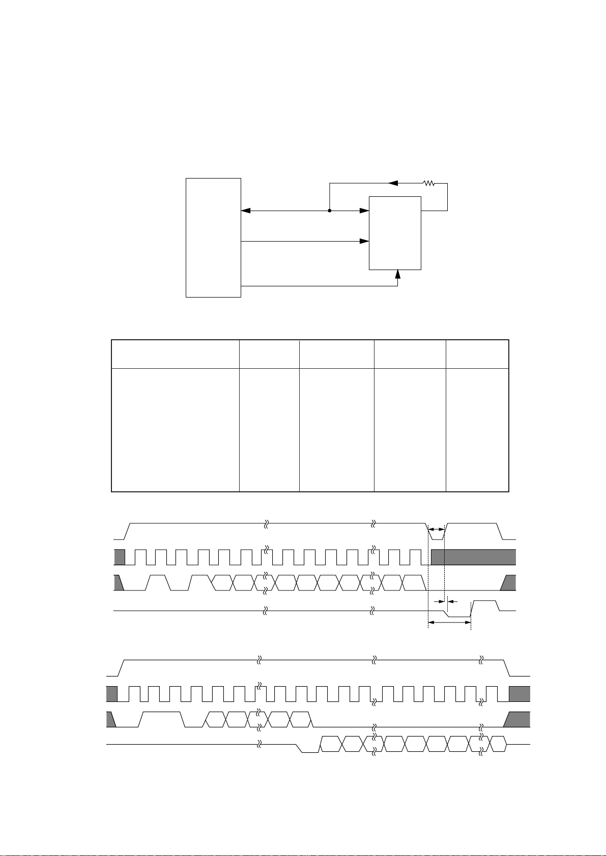
The BR93LC46A on the main control board is an electrical erasable/programmable ROM of 64bit x 16-bit configuration. Data input to and output from the ROM are bidirectionally transferred
in units of 16 bits through I/O port (EEPRMDT-P) in serial transmission synchronized with a clock
signal from the CPU.
The EEPROM operates in the following instruction modes.
Instruction Start bit Operation Address Data
Read (READ) 1 10 A5 to A0
Write Enabled (WEN) 1 00 11XXXX
Write (WRITE) 1 01 A5 to A0 D15 to D0
Write All Address (WRAL) 1 00 01XXXX D15 to D0
Write Disabled (WDS) 1 00 00XXXX
Erase 1 11 A5 to A0
Chip Erasable (ERAL) 1 00 10XXXX
IC6
CPU
39
38
37
EEPRMDT-P
EEPRMCS-P
EEPRMCLK-P
code
3
DI DO
EEPROM
1
CS
IC4
4
SK
2
Write cycle timing (WRITE)
CS
SK
DI
DO
1 2 4 9 10 25
10 1
HIGH-Z
Read cycle timing (READ)
CS
SK
DI
DO
HIGH-Z
12
110
A5 A4 A1 A0 D15
4
A5 A4 A1 A0
910
- 7 -
Min. 450 ns
D14
D15 D14 D1 D00 D15 D14
D1 D0
Max. 500 ns
BUSY READY
Max. 10 ms
25 26
STATUS
3.5 Parallel Interface
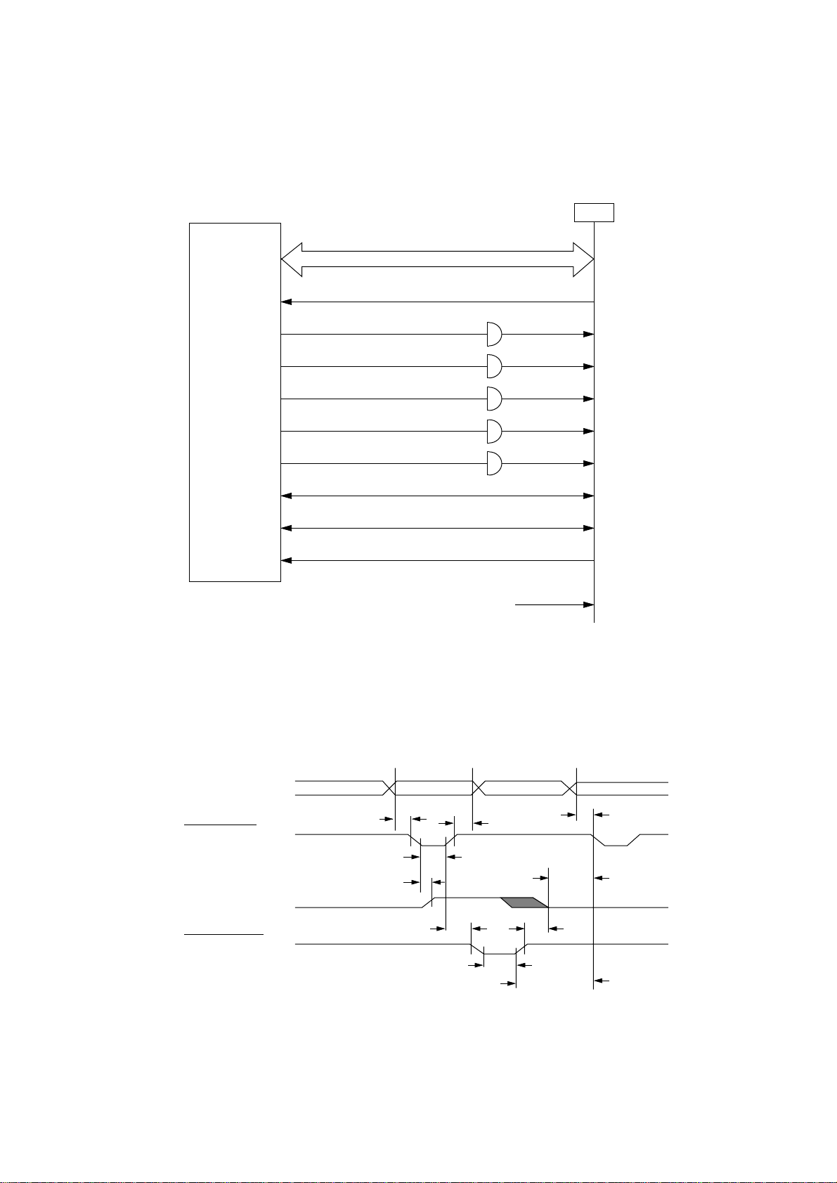
Parallel data is received from a host system via parallel interface which is compliant to the
IEEE1284 specification.
IC6
CPU
65 to 68, 71 to 74
64
78
77
79
80
81
82
83
84
PSTB-N
BUSY-P
ACK-N
PE-P
SEL-P
FAULT-N
IPRIME-N
SELIN-N
AUTOFD-N
PDATA1-P to PDATA8-P
+5V or High level
IC7
2 to 9
11
10
12
13
32
31
36
14
18
CN4
1
DATA8-P
to
DATA1-P
STB-N
BUSY-P
ACK-N
PE-P
SEL-P
FAULT-N
IPRIME-N
SELIN-N
AUTOFEED-N
+5V
Compatible mode
The CPU sets a BUSY-P signal to ON at the same time when it reads the parallel data (PDATA1P to PDATA 8-P) from the parallel port at the fall of PSTB-N signal. Furthermore, it makes the
store processing of received data into a receive buffer terminate within a certain fixed time and
outputs an ACK-N signal, setting the BUSY-P signal to OFF.
PARALLEL DATA
(DATA BITs 1 to 8)
0.5 µs min.
DATA STROBE
0.5 µs min.
0.5 µs max.
BUSY
0 min.
ACKNOWLEDGE
0.5 µs to 10 µs
0.5 µs min.
0.5 µs min.
0 min.
0 min.
0 min.
- 8 -
3.6 LED Lamp Control
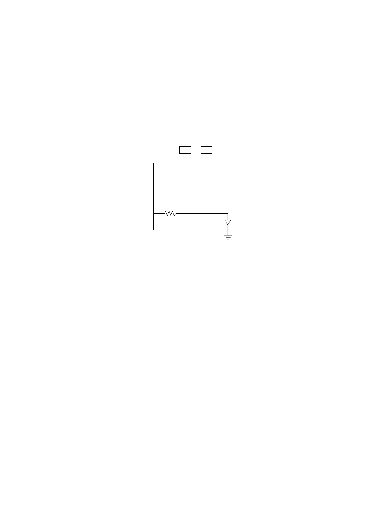
There is an LED lamp on the high voltage power supply board which is connected to and controled
by the CPU on the main control board.
The light from the LED lamp can be seen on the Lens Cover through the LED Lens.
CN1
main control board high voltage power supply board
IC6
CPU
LED-P
41
CN1
- 9 -
3.7 LED Head Control
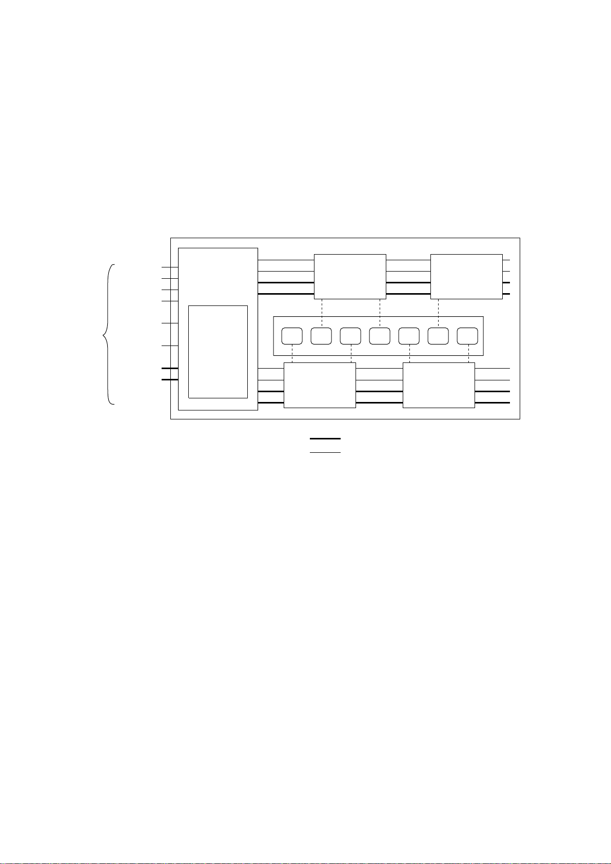
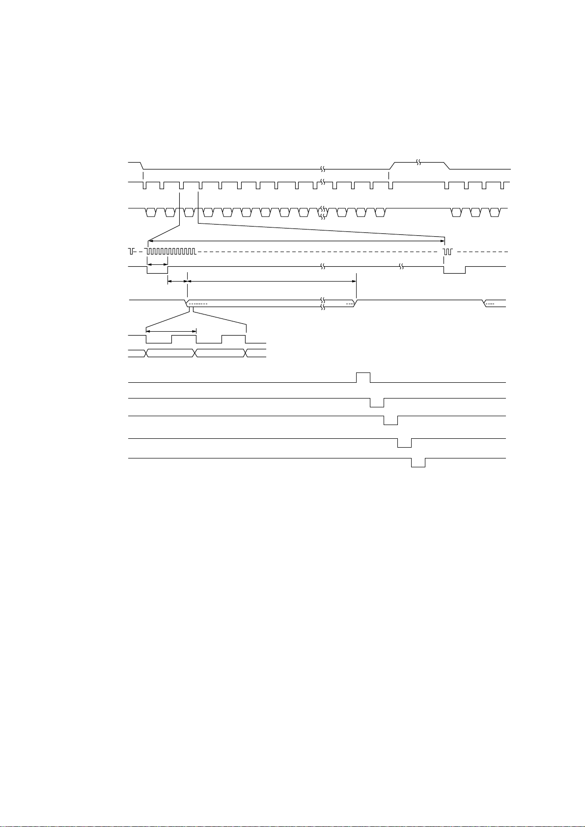
An LED correcting head, which is capable of correcting the illumination of the LED for each dot,
is being used in this printer. LED illumination correction function of 16 steps is carried out by using
an EEPROM which is installed in the LSI that maintains the LED illumination correction values,
and an LED correction drivers (MSM6731BWAF or MSM6732BWAF) together as a pair.
The LED correcting head consists of the correction control LSI (MSM6730WAF), LED drivers
(MSM6731BWAF or MSM6732BWAF), and an LED array.
From
CPU
STRB0-N
STRB1-N
STRB2-N
STRB3-N
LOADI
CLOCKI
DATAI0
DATAI1
MSM6730
WAF
EEPROM
Correction
Values
LED Driver
MSM6732BWAF
LED Array
LED LED LED LED LED LED LED
LED Driver
MSM6731BWAF
Printing and correction data combined sign
Correction data signal line
LED Driver
MSM6731BWAF
LED Driver
MSM6732BWAF
- 10 -
Page
synchronous
signal*
Line
synchronous
signal*
VDT-P
0.78 msec
VCLK-P
VDT-P
VCLK-P
VDT-P
VLD-P
VSTB4-N
VSTB3-N
VSTB2-N
VSTB1-N
* CPU internal signal
8 bits
8 bits
0.3 µs
4992 bits
- 11 -
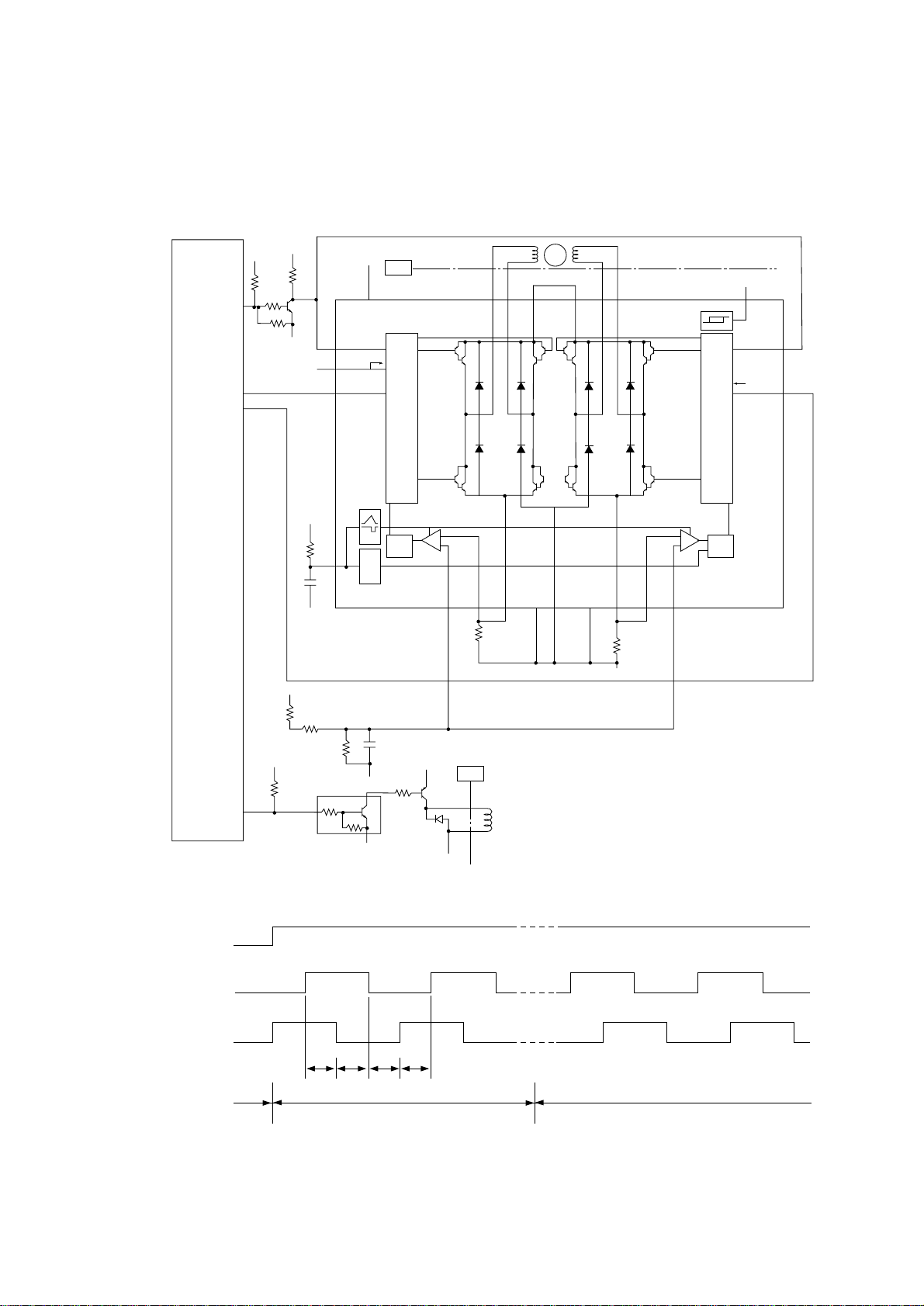
3.8 Motor and clutch control
The electromagnetic clutch is driven by a control signal from the CPU and the drive circuit shown
below.
The main motor is driven by the control signals from the CPU and the driver IC.
CPU
DMON
DMP1
DMP2
+5V
98
96
97
+5V
0V
+5V
Main Motor
8
Out4Vmm A Vmm B
+5V
IC10
27
18
26
+5V
19
ENA A
To Out3, 4Logic
DECAY
CN7
M
+26V OPEN
37 1 1412 24
Out2 Out3
Out1
SW1 SW3
SW1 SW3
PHASE A PHASE B
GATE CIRCUIT
SW4SW2
SW4SW2
+5V
0V
25
BRUNK
OSC
Current
Q
-
R
+
S
Sensor
Vref A Vref B
Vs A Vs BRs A Rs BLG A PG LG B
23 22 28 15 10 21 20TAB5
Current
Sensor
0V
ALARM
120°C 140°C
GATE CIRCUIT
RQ
+
S
ENA B
Signal of
DECACY
16
17
RMON
(1) Main motor
DMON-P
DMPH1-P
DMPH2-P
Rotation
+5V +26V
0V
99
0V
T0 T1 T2 T3
Forward rotation
CN8
Electromagnetic clutch
0VP
Reverse rotationStop
Operation at normal speed: T0 to T3 = 0.781 ms
- 12 -
(2) Motor drive control
Time T0 to T3 determines the motor speed, while the phase different direction between
phase signals DMPH1-P and DMPH2-P determines the rotation direction. DMON-P signal
control a motor coil current. According to the polarity of the phase signal, the coil current flow
as follows:
1) +26V → SW1 → motor coil → SW4 → resistor → earth, or,
2) +26V → SW3 → motor coil → SW2 → resistor → earth
The drop voltage across the resistor is input to comparator, where it is compared with a
reference voltage. If an overcurrent flows, a limiter operates to maintain it within a certain
fixed current.
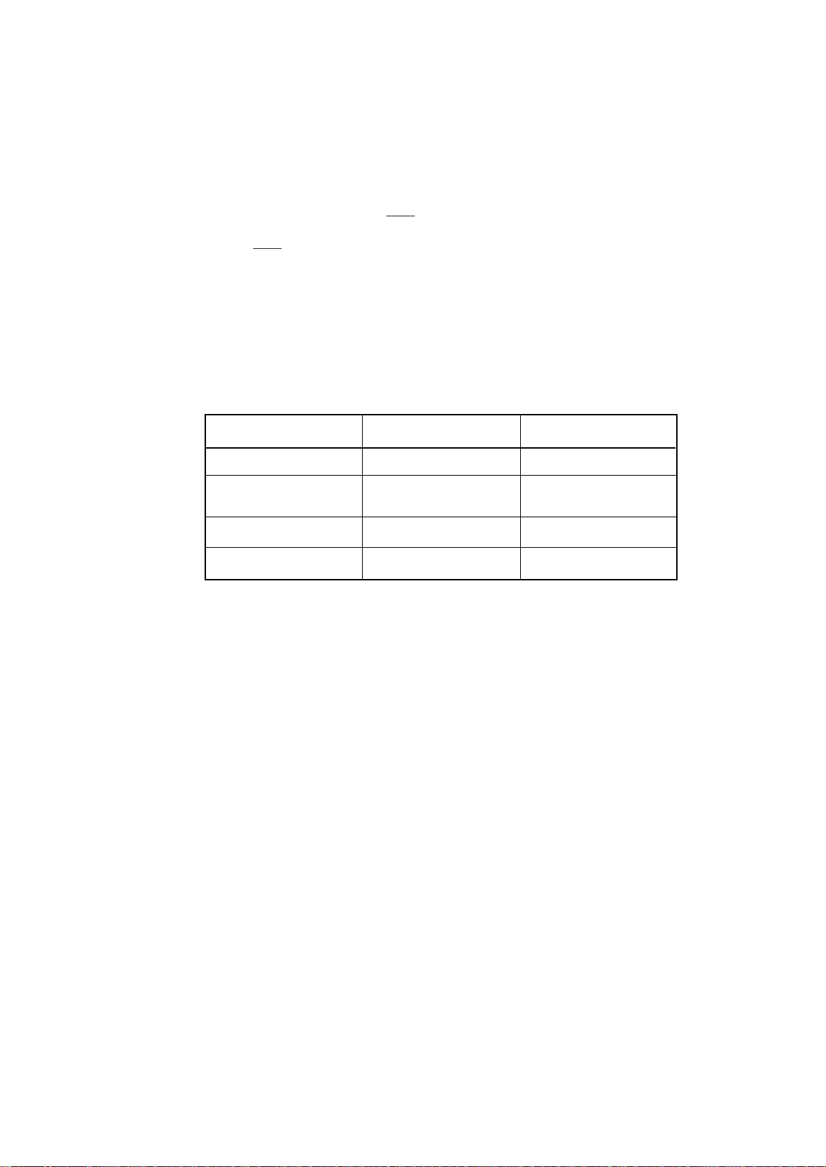
(3) Electromagnetic clutch control
Mechanical operation mode is switched by the combination of the clutch status and the
direction of motor rotation.
clutch status
off
off
on
on
rotation direction
Forward
Reverse
Forward
Reverse
operation mode
cleaning
Hopping from manual
feed slot
illegal operation
Hopping from tray
- 13 -
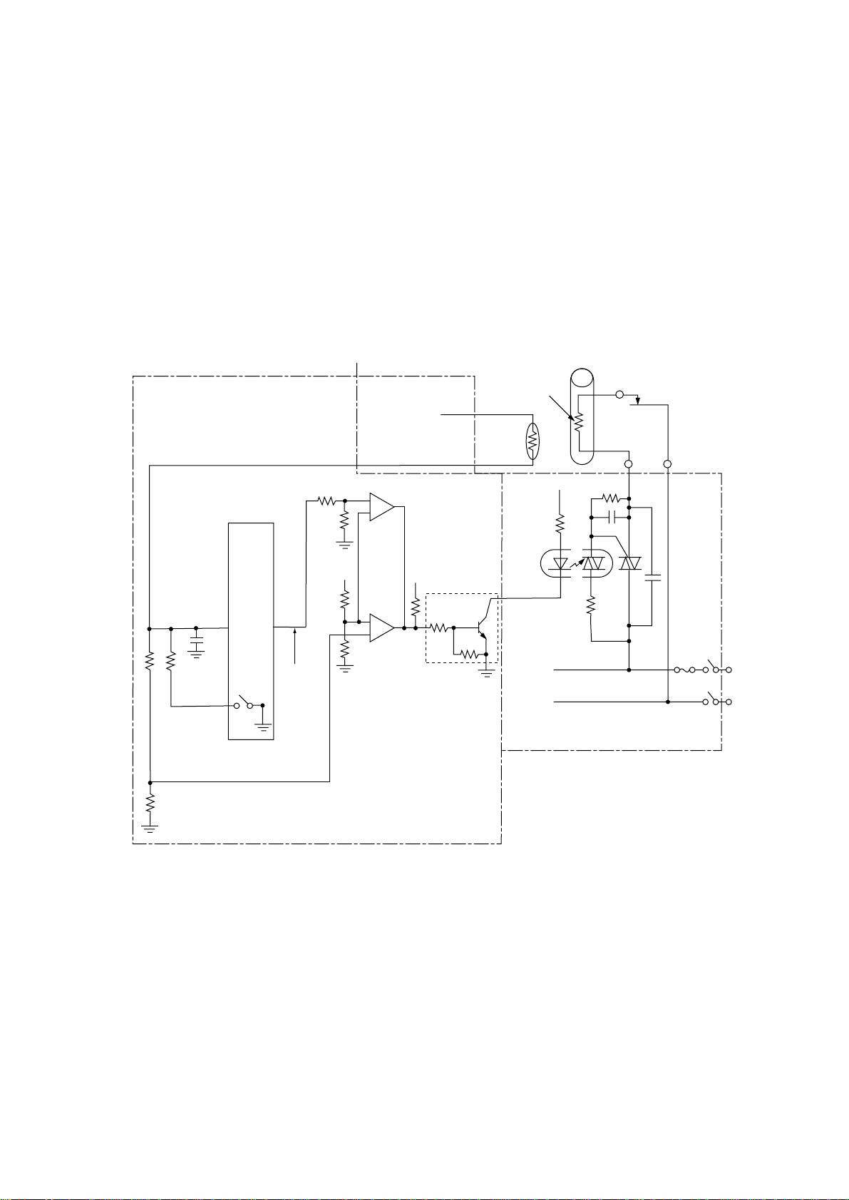
3.9 Fuser Temperature Control
The temperature change in a heat controller is converted into the electric potential TEMP
corresponding to the change in the resistance value of a thermistor, and the resultant potential
is fed back to the control circuit. The CPU performs ON/OFF control of the HEATON-P signal to
keep the heat roller temperature constant in accordance with the state at which the thermistor
voltage (TEMP) is read into directly by the AD converter of the CPU.
When the paper thickness is set on the menu of the host, the temperature is adjusted to the
targeted thickness accordingly.
Main Control Board
CPU
TEMP
27
AI4
(A/D)
THCHK-N
34
85
HEATON-P
High voltage power
supply board
IC20
5
+
6
-
7
+5V +5V
IC20
3
+
2
-
1
+5V
Thermistor
HEATON-N
Heater
Thermostat
Heat Roller
+5V
ACIN
Power supply unit
- 14 -
 Loading...