OKI MSM6636BGS-K Datasheet

E2E1035-27-Y2
¡ Semiconductor MSM6636B
¡ Semiconductor
This version: Jan. 1998
Previous version: Nov. 1996
MSM6636B
SAE-J1850 Multiplex Communication Protocol Conformity Transmission Controller for
Automotive LAN
GENERAL DESCRIPTION
The MSM6636B is a transmission controller for automotive LAN based on data communication
protocol SAE-J1850. This device can realize a data bus topology bus LAN system with a PWM
bit encoding method (41.6 kbps). In addition to a protocol control circuit, MSM6636B has an
enclosed quartz oscillation circuit, host CPU interface (parallel interface), a transmit/receive
buffer, and a bus receiver circuit that decreases the burden on the host CPU.
FEATURES
• Based on SAE-J1850 CLASS B DATA COMMUNICATION NETWORK INTERFACE (issued
August 12, 1991)
• Non-destructive collision and priority control using CSMA/CD
• Internal transmit buffer (1 frame) and receive buffer (2 frames)
• Modulating/demodulating: PWM (Pulse Width Modulation)
• Transmission speed: 41.6 kbps
• Multi-address setting with physical addressing: 1 type / functional addressing: 15 types
• Address filter function by multi-addressing (broadcasting possible)
• Automatic retransmission function by arbitration loss and non ACK
• Three types of in-frame response support:
q Single-byte response from a single node
w Multi-byte response from a single node (with CRC code)
e Single-byte response from multiple nodes (ID response as ACK)
• Error detection by cyclic redundancy check (CRC)
• Various communication error detections
• Dual-wire bus abnormality detection by internal bus receiver and fault tolerance function
• Host CPU interface is accessed in parallel
• Sleep function
Low current consumption mode by oscillation stop (IDS Max < 50µA)
SLEEP / WAKE UP control from host CPU, WAKE UP via LAN bus
• Package: 24-pin plastic SOP (SOP24-P-430-1.27-K) (Product name : MSM6636BGS-K)
1/13

¡ Semiconductor MSM6636B
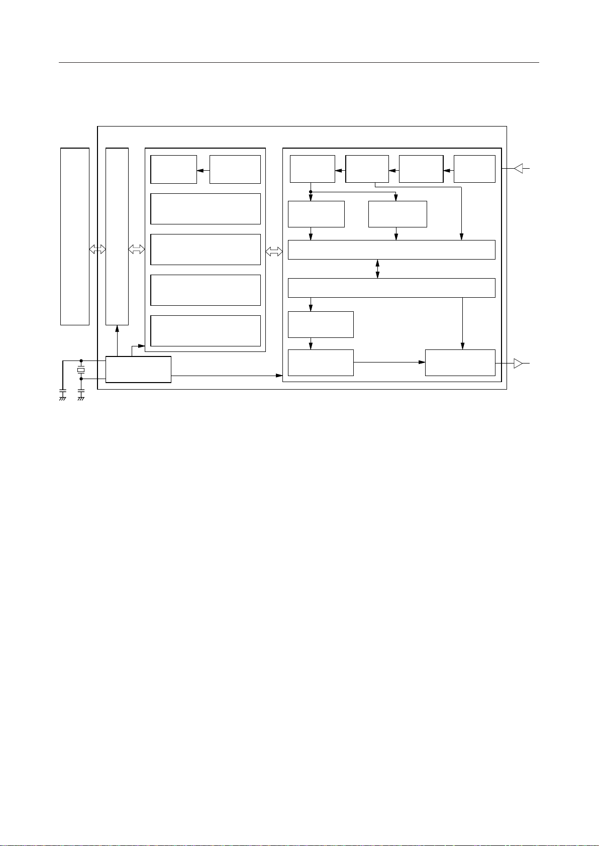
BLOCK DIAGRAM
CPU
x'tal
Buffer Register
Receive
Register
Address Register
Status Register
Parallel Interface
Transmission Register
Response Register
Clock
Generator
Receive
Buffer
S-P
Converter
CRC
Checker
Generator
Converter
MSM6636B
CRC
P-S
LAN Controller
PWM
Decoder
Receive Controller
Transmission Controller
Degital
Filter
Address
Filter
Bus
Receiver
PWM
Encoder
LAN
Bus
Input
LAN
Bus
Output
2/13

¡ Semiconductor MSM6636B
PIN CONFIGURATION (TOP VIEW)
24
23
22
21
20
19
AD3
18
17
16
15
14
13
DD
1
2
3
4
5
6
7
8
9
10
11
12
WR DV
RD AD7
ALE AD6
INT AD5
RES AD4
AV
BO– AD2
BI– AD1
BI+ AD0
BO+ CS
AGND OSC0
DGND OSC1
24-Pin Plastic SOP
PIN DESCRIPTION
Pin Description
Symbol
WR1I
RD2I
ALE3I
INT4O
RES5I
6—
AV
DD
BO–7O
BI–8I
BI+9I
BO+10 O
AGND11 —
DGND12 —
OSC113 O
OSC014 I
CS15 I
AD0-716-23 I/O
24 —
DV
DD
Type
Data write enable input pin
Data read enable input pin
Address latch input pin
Interrupt output pin
Reset input pin
Analog power supply voltage
LAN—BUS output –
LAN—BUS input –
LAN—BUS input +
LAN—BUS output +
Analog ground pin
Digital ground pin
Crystal (or ceramic resonator) oscillation output
Crystal (or ceramic resonator) oscillaiton input
Chip select input pin
Address input/data input-output pin
Digital power supply voltage
DD
3/13

¡ Semiconductor MSM6636B
ABSOLUTE MAXIMUM RATINGS
DGND=AGND=0V
Parameter
Power Supply Voltage
Input Voltage
Output Voltage V
Power Dissipation P
Storage Temperature T
Symbol
DVDD, AV
V
I
O
D(SOP)
STG
DD
1
*
*1 24-pin SOP package power dissipation
Power Dissipation Curve
< 24-pin SOP package>
1000
[mW]
780
Condition Rating
—
AVDD=DV
AVDD=DV
DD
DD
–0.3 to +7.0
–0.3 to DVDD+0.3
–0.3 to DVDD+0.3
Ta=25°C 780
— –55 to +150
Unit
V
V
V
mW
°C
D(SOP)
500
–40 25 125 150
Power dissipation P
Ambient temperature Ta (°C)
4/13
 Loading...