

E2D0011-27-43
SUNSTAR单片机专用电路 http://www.icasic.com/ TEL: 0755-83387030 FAX:0755-83376182 E-MAIL:szss20@163.com
SUNSTAR半导体集成电路 http://www.icasic.com/ TEL: 0755-83387016 FAX:0755-83376182 E-MAIL:szss20@163.com
¡ Semiconductor
¡ Semiconductor
This version: Jan. 1998
Previous version: May. 1997
MSM6585
MSM6585
ADPCM Voice Synthesis IC
GENERAL DESCRIPTION
The MSM6585 is an version-up product of the MSM5205 voice synthesis IC. Mainly improved points
are improvement for the precision of an internal DA converter, a built-in low-pass filter, and
expansion on the sampling frequency. The MSM6585 does not include a control circuit to drive an
external memory similar to the MSM5205. Therefore, the MSM6585 can be connected with not only
semiconductor memories, but other memory media (CD-ROM, etc.) by the control of CPU.
FEATURES
• 4-bit ADPCM method
• Built-in 12-bit DA converter
• Built-in low-pass filter (LPF) (–40dB/oct)
• Sampling frequencies: 4k/8k/16k/32kHz
• Master clock frequency (ceramic oscillator) : 640kHz
• Voice data synthesis : Supported by voice analysis editing tools AR76-202 and AR203
• Package options :
18-pin plastic DIP (DIP18-P-300-2.54) (Product name : MSM6585RS)
24-pin plastic SOP (SOP24-P-430-1.27-K) (Product name : MSM6585 GS-K)
30-pin plastic SSOP (SSOP30-P-56-0.65-K) (Product name : MSM6585 GS-AK)
DIFFERENCES BETWEEN MSM6585 AND MSM5205
MSM6585 MSM5205
• Master clock frequency: 640kHz 384kHz
• Sampling frequency: 4k/8k/16k/32kHz 4k/6k/8kHz
• ADPCM bit length: 4-bit 3-bit/4-bit
• DA Converter: 12-bit 10-bit
• Low-pass filter: Included (–40dB/oct) Not included
• Overflow preventing circuit: Included Not included
• Power supply voltage: 4.5 to 5.5V 3.0 to 6.0V
• Operating current consumption: 10mA 4mA
• Operating temperature: –40 to +85°C –30 to +70°C
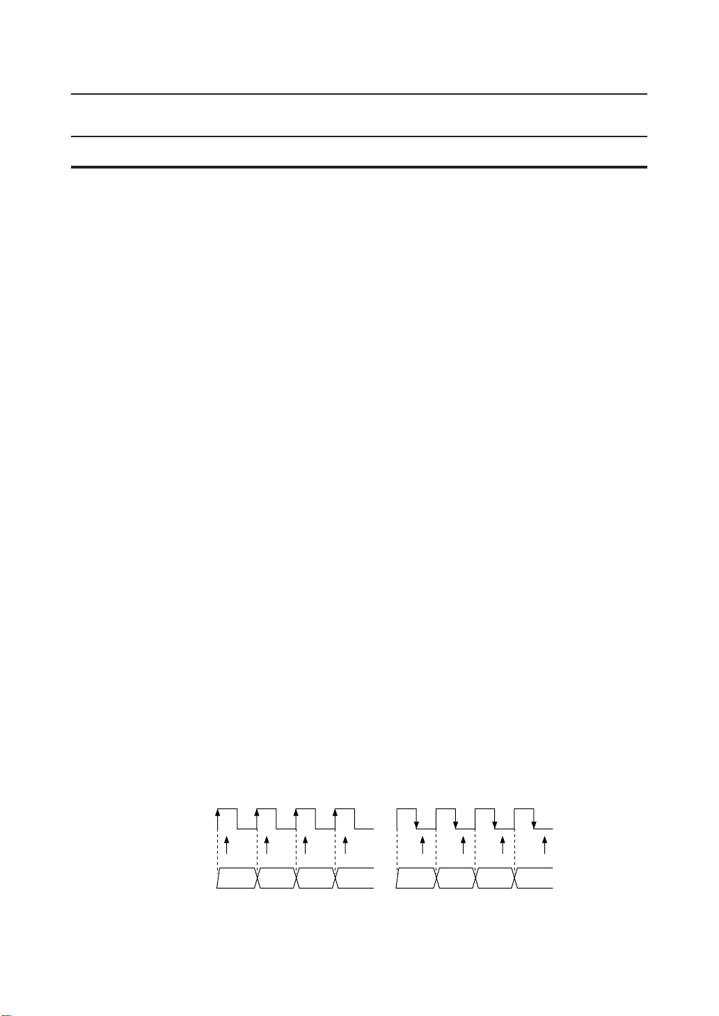
• D3 to D0 input timing
VCK (O)
D3 - D0
input timing
ADPCM Data
1/14
¡ Semiconductor
SUNSTAR单片机专用电路 http://www.icasic.com/ TEL: 0755-83387030 FAX:0755-83376182 E-MAIL:szss20@163.com
SUNSTAR半导体集成电路 http://www.icasic.com/ TEL: 0755-83387016 FAX:0755-83376182 E-MAIL:szss20@163.com
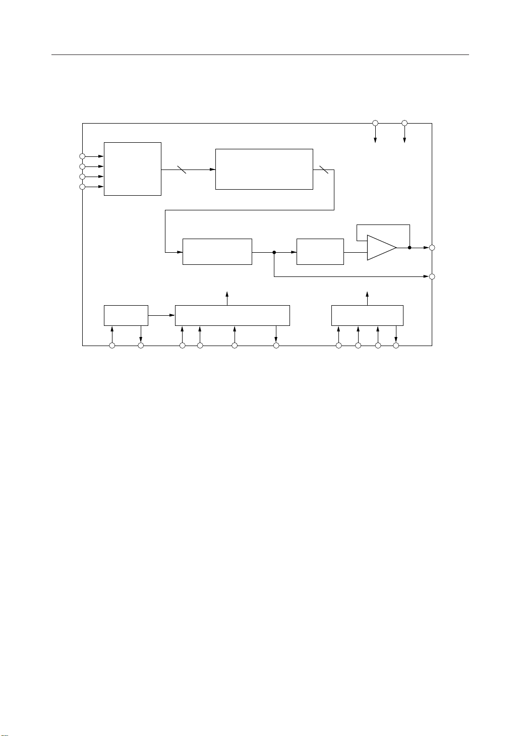
BLOCK DIAGRAM
MSM6585
GND
V
DD
D3
D2
D1
D0
4124-Bit
LATCH
12-Bit DAC LPF
OSC Timing Controller TEST CIRCUIT
XT XT S1 S2 RESET VCK T1 T2 T3 T4
ADPCM
Synthesizer
–
+
AOUT
DAO
2/14
¡ Semiconductor
SUNSTAR单片机专用电路 http://www.icasic.com/ TEL: 0755-83387030 FAX:0755-83376182 E-MAIL:szss20@163.com
SUNSTAR半导体集成电路 http://www.icasic.com/ TEL: 0755-83387016 FAX:0755-83376182 E-MAIL:szss20@163.com
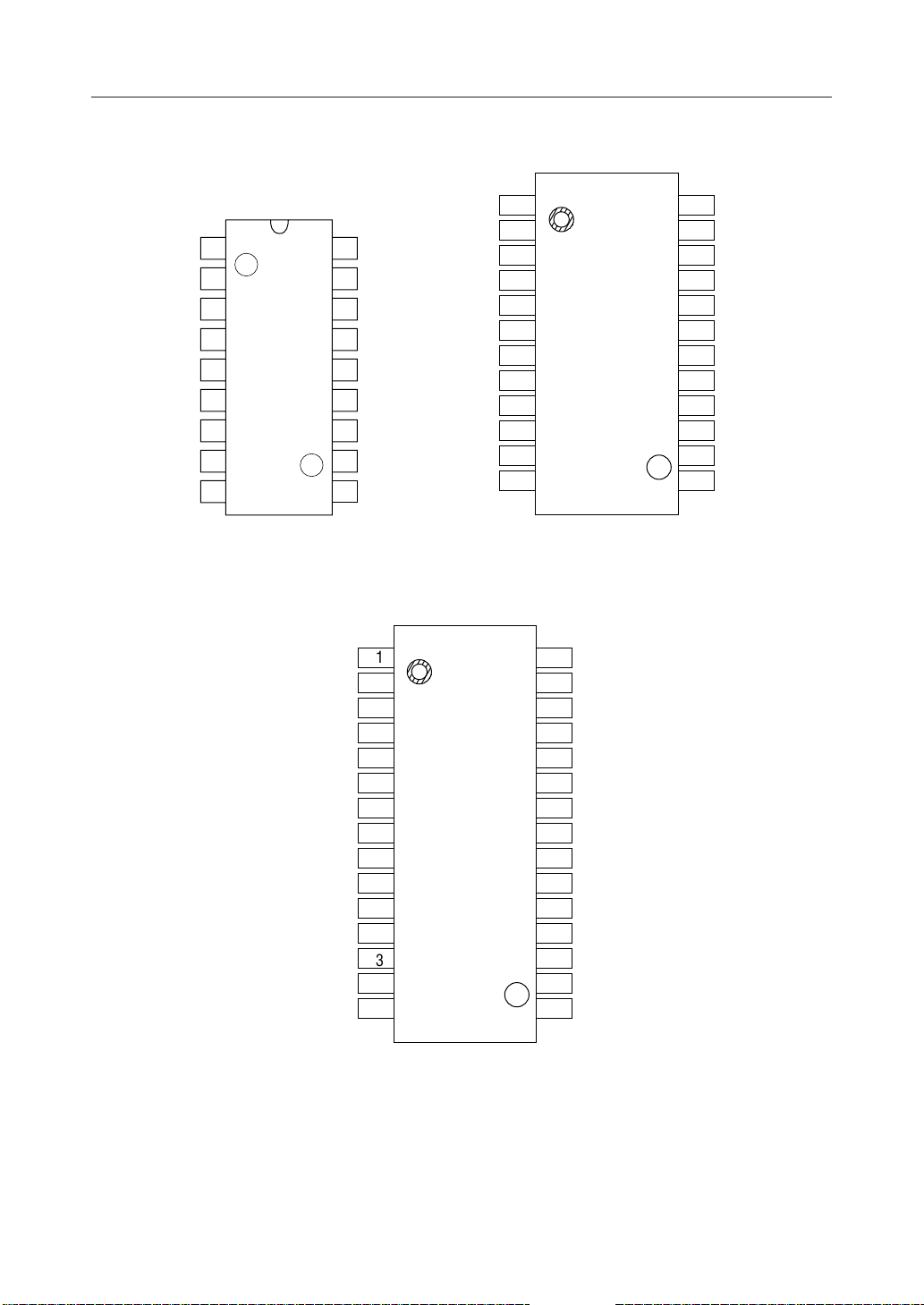
PIN CONFIGURATION (TOP VIEW)
MSM6585
S1
1
S2
2
T3
3
D0
4
D1
5
D2
6
D3
7
T4
8
GND
9
18-Pin Plastic DIP
18
17
16
15
14
13
12
11
10
S1
S2
NC
NC
NC
T3
D0
D1
D2
D3
NC
NC
NC
T4
GND
V
DD
XT
XT
RESET
VCK
T2
T1
DAO
AOUT
1
2
3
4
5
6
7
8
9
10
11
12
13
14
15
S1
S2
T3
NC
D0
NC
D1
D2
NC
D3
T4
GND
1
2
3
4
5
6
7
8
9
10
11
12
NC : No connection
24-Pin Plastic SOP
30
V
DD
XT
29
NC
28
NC
27
NC
26
XT
25
RESET
24
VCK
23
T2
22
T1
21
NC
20
NC
19
NC
18
DAO
17
AOUT
16
24
23
22
21
20
19
18
17
16
15
14
13
V
DD
XT
XT
NC
RESET
NC
VCK
T2
T1
NC
DAO
AOUT
NC : No connection
30-Pin Plastic SSOP
3/14
¡ Semiconductor
SUNSTAR单片机专用电路 http://www.icasic.com/ TEL: 0755-83387030 FAX:0755-83376182 E-MAIL:szss20@163.com
SUNSTAR半导体集成电路 http://www.icasic.com/ TEL: 0755-83387016 FAX:0755-83376182 E-MAIL:szss20@163.com
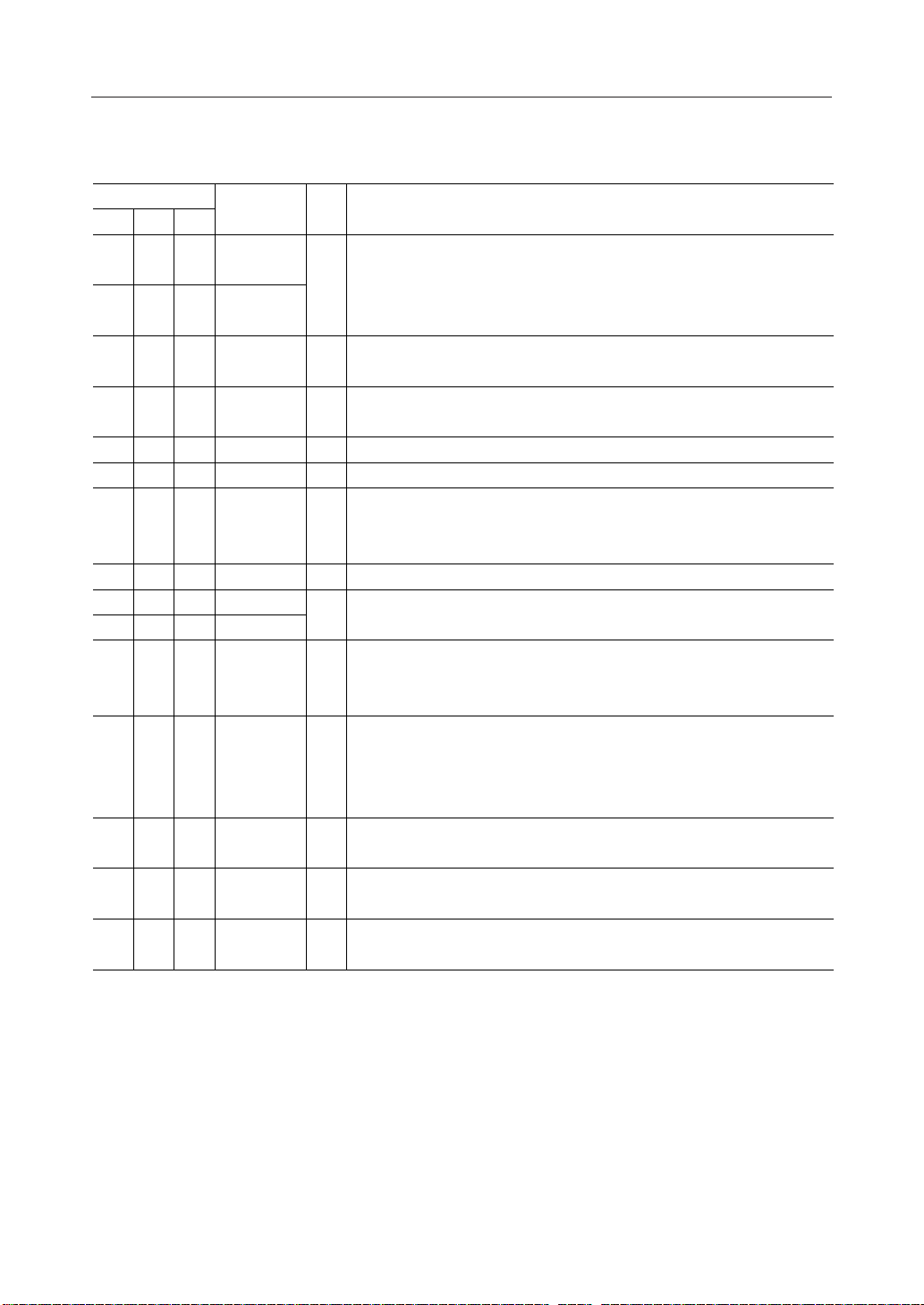
PIN DESCRIPTION
MSM6585
Pin
DIP SOP
SSOP
111
336
5, 7,
4-7
8, 10
7-10
81114
91215
10 13 16
11 14 17
12 16 21
14 18 23
15 20 24
16 22 25
17 23 29
18 24 30
Symbol Type Description
S1
S2222
T3 I
D0-D3 I
T4 O
GND —
Pins to determine the sampling frequency.
The sampling frequencies of 32k, 16k, 8k, and 4kHz can be selected by
I
combinations. (See the sampling frequencies in FUNCTIONAL
DESCRIPTION on the selection of combinations.)
Pin to test the internal circuit. Set this pin to a high level or make it open
because it has a built-in pull-up resistor.
Input pins for ADPCM data.
Pin to test the internal circuit. Make this pin open.
Pin to test the internal circuit. Make this pin open.
Ground pin
Pin to output the analog voice from the low-pass filter. Connect a 0.01 mF
AOUT O
capacitor to this pin. (See the AOUT connecting circuit in FUNCTIONAL
DESCRIPTION on the connecting circuit.)
DAO O
T1
T213 17 22
Pin to output the analog voice from the DA converter.
Pins to test the internal circuit. Set these pins to a low level or make them
I
open because pull-down resistors are included.
This pin outputs the sampling frequency selected by the combinations of
VCK O
S1 and S2.
The voice synthesis starts or stops by synchronizing with VCK.
Reset pin. The voice synthesis circuit is initialized by synchronizing with
RESET I
VCK. If this pin is set to a high level, the D0 to D3 data inputs are disabled
by synchronizing with VCK. The AOUT and DA0 pins output 1/2 V
become the state of no voice.
XT I
XT O
V
DD
Pin to connect an oscillator. When the external clock is used, input it
from this pin.
Pin to connect an oscillator.
When the external clock is used, make this pin open.
Power supply pin. Insert a bypass capacitor of 0.1 mF or more between
—
this pin and the GND pin.
DD
and
4/14
¡ Semiconductor
SUNSTAR单片机专用电路 http://www.icasic.com/ TEL: 0755-83387030 FAX:0755-83376182 E-MAIL:szss20@163.com
SUNSTAR半导体集成电路 http://www.icasic.com/ TEL: 0755-83387016 FAX:0755-83376182 E-MAIL:szss20@163.com
ABSOLUTE MAXIMUM RATINGS
Parameter
Power Supply Voltage
Input Voltage
Storage Temperature
Symbol
V
DD
V
IN
T
STG
Condition
Ta = 25°C
Ta = 25°C
—
Rating
–0.3 to +7.0
–0.3 to V
–55 to +150
DD
+0.3
MSM6585
(GND=0 V)
Unit
V
V
°C
RECOMMENDED OPERATING CONDITIONS
Parameter
Power Supply Voltage
Operating Temperature
Master Clock Frequency
DD
op
OSC
Condition Range UnitSymbol
— 4.5 to 5.5 VV
— –40 to +85 °CT
oscillator connection 640 kHzf
ELECTRICAL CHARACTERISTICS
DC Characteristics
Parameter
"H" Input Voltage
"L" Input Voltage
"H" Output Voltage
"L" Output Voltage
"H" Input Current
"H" Input Current
"H" Input Current
"L" Input Current
"L" Input Current
"L" Input Current
Current Consumption
DA Output Relative Error
DA Output Impedance
LPF Load Resistance
Symbol
V
IH
V
IL
V
OH
V
OL
I
IH1
I
IH2
I
IH3
I
IL1
I
IL2
I
IL3
I
DD
| V
DAE
R
DAO
R
AOUT
S1, S2, D0 - D3, T3: V
|
Condition Unit
—
—
VCK: I
OH
= –40mA
VCK: IOL = 40mA
T1, T2, RESET: V
XT: VIH = V
IH
DD
T3: VIL = 0V
S1, S2, D0 - D3, T1, T2,
IL
=0V
IL
=0V
RESET: V
XT=V
f
=640kHz, No load
osc
No load
—
—
(VDD=4.5 to 5.5V, GND=0V, Ta=–40 to +85°C)
= V
IH
DD
= V
DD
Min.
0.8¥V
–0.1
V
DD
—
20
—
—
–400
–10
–20
—
—
10
50
–0.4
DD
Typ.
—
—
—
—
150
—
—
–120
—
—
5
—
—
—
Max.
V
0.2¥V
(GND = 0V)
+0.1
DD
DD
—
0.4
400
10
20
–20
—
—
10
40
40
—
V
V
V
V
mA
mA
mA
mA
mA
mA
mA
mV
kW
kW
5/14

¡ Semiconductor
SUNSTAR单片机专用电路 http://www.icasic.com/ TEL: 0755-83387030 FAX:0755-83376182 E-MAIL:szss20@163.com
SUNSTAR半导体集成电路 http://www.icasic.com/ TEL: 0755-83387016 FAX:0755-83376182 E-MAIL:szss20@163.com
AC Characteristics
MSM6585
Parameter
Original Oscillation
Duty Cycle
RESET Input Pulse Width
Data Setup Time
Data Hold Time
f
duty
t
W(RST)
t
S
t
H
f
SAM
= 4kHz
= 8kHz
=16kHz
=32kHz
—
...
t
= 250ms
VCK
...
...
...
= 125ms
= 62.5ms
=31.25ms
Min. Typ. Max.
50 60 %40
2¥t
t
VCK
—
VCK
—
—
—
/2
—
—
UnitSymbol Condition
ms
3
ms
ms
When data is shared with the MSM5205, note that the D3 to D0 selection timings of the MSM6585
and MSM5205 are different. (Refer to DIFFERENCES BETWEEN MSM6585 AND MSM5205.)
TIMING DIAGRAM
VCK (O)
RESET (I)
D3 - D0 (I)
IC internalD3 - D0
selection timings
AOUT, DAO (O)
t
VCK
t
W(RST)
t
H
ADPCM1 ADPCM2 ADPCMN
t
S
t
VCK/8
ADPCM
N+1
The VCK clock rising and falling edges are reversed between the MSM5205 and the MSM6588, as
indicated in DIFFERENCES BETWEEN MSM6585 AND MSM5205.
Note that the MSM6585 cannot accept data if the MSM5205 controls to repeat valid and invalid each
half cycle, when the MSM5205 is replaced with the MSM6585.
6/14

¡ Semiconductor
SUNSTAR单片机专用电路 http://www.icasic.com/ TEL: 0755-83387030 FAX:0755-83376182 E-MAIL:szss20@163.com
SUNSTAR半导体集成电路 http://www.icasic.com/ TEL: 0755-83387016 FAX:0755-83376182 E-MAIL:szss20@163.com
FUNCTIONAL DESCRIPTION
1. Sampling Frequency
The relationship of the sampling frequencies on S1 and S2, and the cutoff frequencies are
listed below.
MSM6585
S1
S2
L
H
L
H
L
L
H
H
Sampling frequency (f
4 kHz
8 kHz
16 kHz
32 kHz
SAM
)
Cutoff frequency (f
1.6 kHz
3.2 kHz
6.4 kHz
12.8 kHz
CUT
)
2. AOUT Connecting Circuit
Connect a 0.01mF capacitor to the AOUT pin. The circuit diagram is as shown below.
MSM6585
AOUT
0.01mF
Amplifier Speaker
Even when the DAO pin is used, connect a 0.01mF capacitor to the AOUT pin. This capacitor is used
for the improvement of a voice quality.
3. Voice Output
The MSM6585 has two voice output pins. The DAO is direct output pin from the internal DA
converter. The AOUT is a pin to output a voice after which the DAO output passed a built-in LPF.
3.1 DA Converter Output Waveform
The output amplitude from the DA converter is max. (4095/4096) ¥ VDD and becomes a stair step
waveform synchronized with the sampling frequency. The DAO output impedance varies in the
ranges from 10kW to 40kW. Therefore, determine the filter constant so that the resistor variation does
not
have influence on the cutoff frequency of the filter.
7/14

¡ Semiconductor
q
)
SUNSTAR单片机专用电路 http://www.icasic.com/ TEL: 0755-83387030 FAX:0755-83376182 E-MAIL:szss20@163.com
SUNSTAR半导体集成电路 http://www.icasic.com/ TEL: 0755-83387016 FAX:0755-83376182 E-MAIL:szss20@163.com
3.2 Low-pass Filter Output
The cutoff frequency of the low-pass filter varies in proportion to the sampling frequency.
The following figure shows the low-pass filter characteristics in the sampling frequency
8kHz.
0
–20
–40
Damping factor (dB)
–60
MSM6585
4. Oscillation
Following show external circuit diagrams using a ceramic resonator, KBR-640B made by
Kyocera Corp. and CSB640P made by Murata MFG. Co., Ltd.
XT XT
220pF
100 1k 10k
uency (Hz
Fre
KBR-640B used
MSM6585
640kHz
220pF
100pF
CSB640P used
MSM6585
XT XT
1MW
640kHz
100pF
8/14

¡ Semiconductor
SUNSTAR单片机专用电路 http://www.icasic.com/ TEL: 0755-83387030 FAX:0755-83376182 E-MAIL:szss20@163.com
SUNSTAR半导体集成电路 http://www.icasic.com/ TEL: 0755-83387016 FAX:0755-83376182 E-MAIL:szss20@163.com
APPLICATION CIRCUITS
Centronics Interface Circuit (sampling frequency : 8kHz)
MSM6585
+5V
BUSY
STROBE
RESET
D0
D1
D2
D3
D4
D5
D6
D7
1
6
MSM4013
3
5
8
7
12 9 13
9
7
5
MSM4019
3
1
6
4
2
15
8
0.1mF
0.1mF
144
10
2
11
14
13
12
11
10
16
S1
RESET
VCK
T4
T1
S2
GND
T2
T3 V
MSM6585
ADPCM
DECODER
D2D3
D1
DD
AOUT
DAO
XT
D0
0.1mF
AMP
0.01mF
XT
640kHz
Centronics Timing Chart
RESET
RES
DATA
STROBE
VCK
KA
KB
BUSY
MIN250msec
First byte
125msec
High nibble
Low nibble
9/14

¡ Semiconductor
SUNSTAR单片机专用电路 http://www.icasic.com/ TEL: 0755-83387030 FAX:0755-83376182 E-MAIL:szss20@163.com
SUNSTAR半导体集成电路 http://www.icasic.com/ TEL: 0755-83387016 FAX:0755-83376182 E-MAIL:szss20@163.com
MSM6585
Example of Interface Circuit with 256K-bit EPROM
The circuit example and timing diagram that used the 256K-bit EPROM are shown below.
A0 ~ A
O0 ~ O11O
MSM4013
RESET
S1Q2D2Q
MSM4013
R1D1S2Q1R
START SW
10kW
0.1mF
100kW
MSM27256
A11A12A13A14O0O4O1O5O2O6O3O
10
11
B1A
12
CL
2
CL
1
CL
2
2
1
KB
D1D2D3D
KA
D0 D1 D2 D3
VCK
MSM6585
RESET
S2 S1
Q
CL
MSM4040
RESET
(MSM4025)
B2A2B3B4A3A
MSM4019
AOUT
Q2Q
1
3
Q
4
CE
7
4
4
640kHz
XT
XT
0.01mF
100kW
M6585 VCK (O)
START SW
M4013 S
1
M4013 Q
M4013 Q
1
2
(M6585 RESET)
(Lower 4-bit)
Q
M4040 Q
M4040 Q
2
1
Q
2
Q
12
3
Q
4
(Upper 4-bit)
10/14

¡ Semiconductor
SUNSTAR单片机专用电路 http://www.icasic.com/ TEL: 0755-83387030 FAX:0755-83376182 E-MAIL:szss20@163.com
SUNSTAR半导体集成电路 http://www.icasic.com/ TEL: 0755-83387016 FAX:0755-83376182 E-MAIL:szss20@163.com
PAD CONFIGURATION
Pad Layout
Product name MSM6585
Function ADPCM voice synthesis IC
Die size ¥ = 2.92 mm, Y = 3.58 mm
Die thickness 350 µm ±30 µm
Pad size 130 µm ¥ 130 µm
Substrate voltage GND
MSM6585
13
16
17
12
20
Y
8
7
X
3
21
Pad Coordiantes
(The die center is located at X=0, Y=0)
PAD No. PAD Name X-axis Y-axis PAD No. PAD Name X-axis Y-axis
1 S1 377 –1635 11 AOUT 38 1635
2 S2 819 –1635 12 DAO –1125 1635
3 T3 1305 –1635 13 T1 –1305 1579
4 D0 1305 –943 14 T2 –1305 1009
5 D1 1305 44 15 VCK –1305 –88
6 D2 1305 1095 16 RESET –1305 –818
7 D3 1305 1635 17 XT –1281 –1635
8 T4 830 1635 18 XT –529 –1635
9AV
10 V
SS
SS
447 1580 19 V
267 1580 20 AV
DD
DD
–299 –1549
–119 –1549
(Unit: mm)
11/14

¡ Semiconductor
SUNSTAR单片机专用电路 http://www.icasic.com/ TEL: 0755-83387030 FAX:0755-83376182 E-MAIL:szss20@163.com
SUNSTAR半导体集成电路 http://www.icasic.com/ TEL: 0755-83387016 FAX:0755-83376182 E-MAIL:szss20@163.com
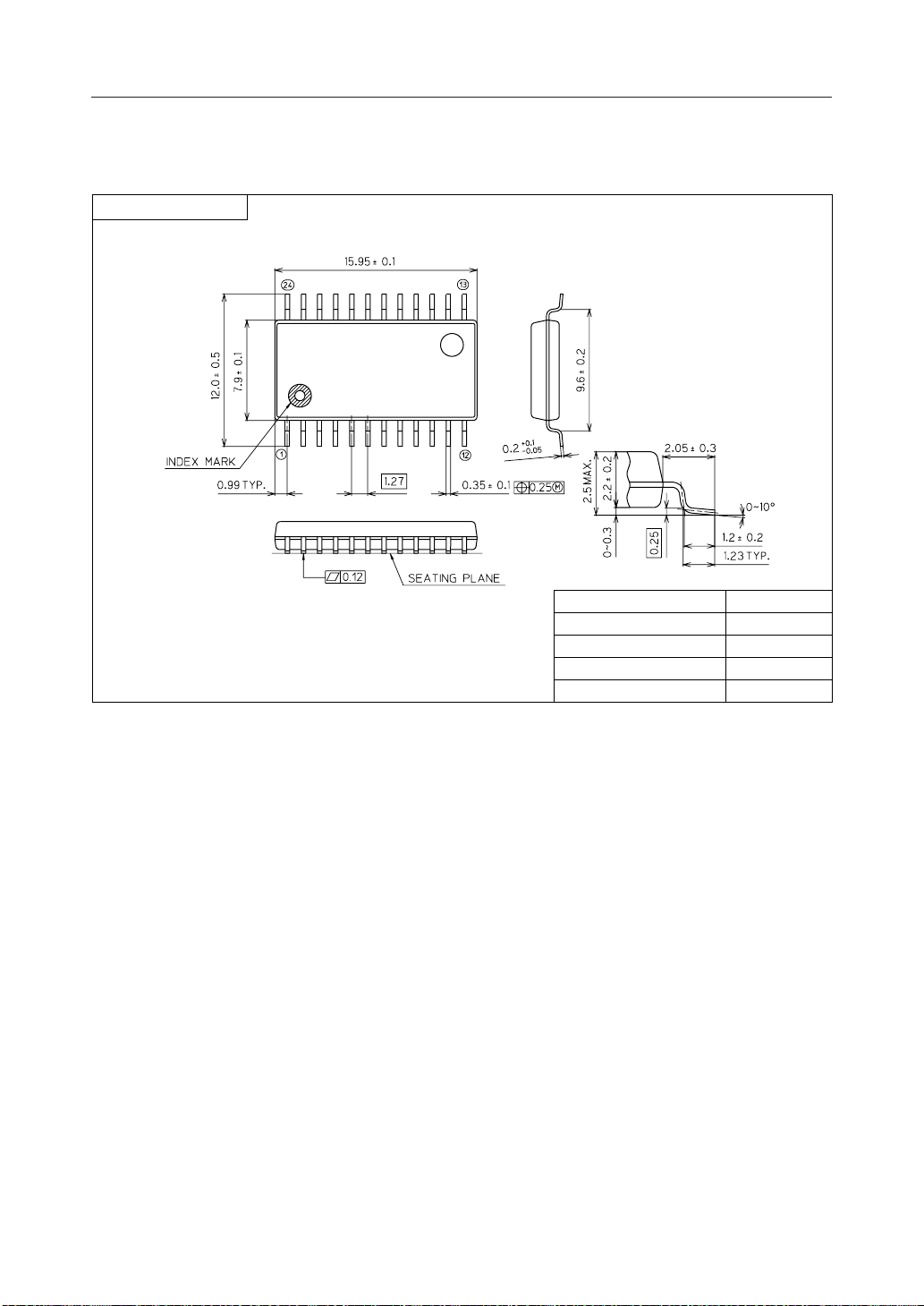
PACKAGE DIMENSIONS
DIP18-P-300-2.54
MSM6585
(Unit : mm)
Package material
Lead frame material
Pin treatment
Solder plate thickness
Package weight (g)
Epoxy resin
42 alloy
Solder plating
5 mm or more
1.30 TYP.
12/14
¡ Semiconductor
SUNSTAR单片机专用电路 http://www.icasic.com/ TEL: 0755-83387030 FAX:0755-83376182 E-MAIL:szss20@163.com
SUNSTAR半导体集成电路 http://www.icasic.com/ TEL: 0755-83387016 FAX:0755-83376182 E-MAIL:szss20@163.com
SOP24-P-430-1.27-K
Mirror finish
MSM6585
(Unit : mm)
Package material
Lead frame material
Pin treatment
Solder plate thickness
Package weight (g)
Epoxy resin
42 alloy
Solder plating
5 mm or more
0.58 TYP.
Notes for Mounting the Surface Mount Type Package
The SOP, QFP, TSOP, SOJ, QFJ (PLCC), SHP and BGA are surface mount type packages, which
are very susceptible to heat in reflow mounting and humidity absorbed in storage.
Therefore, before you perform reflow mounting, contact Oki’s responsible sales person for the
product name, package name, pin number, package code and desired mounting conditions
(reflow method, temperature and times).
13/14

¡ Semiconductor
SUNSTAR单片机专用电路 http://www.icasic.com/ TEL: 0755-83387030 FAX:0755-83376182 E-MAIL:szss20@163.com
SUNSTAR半导体集成电路 http://www.icasic.com/ TEL: 0755-83387016 FAX:0755-83376182 E-MAIL:szss20@163.com
SSOP30-P-56-0.65-K
Mirror finish
MSM6585
(Unit : mm)
Package material
Lead frame material
Pin treatment
Solder plate thickness
Package weight (g)
Epoxy resin
42 alloy
Solder plating
5 mm or more
0.19 TYP.
Notes for Mounting the Surface Mount Type Package
The SOP, QFP, TSOP, SOJ, QFJ (PLCC), SHP and BGA are surface mount type packages, which
are very susceptible to heat in reflow mounting and humidity absorbed in storage.
Therefore, before you perform reflow mounting, contact Oki’s responsible sales person for the
product name, package name, pin number, package code and desired mounting conditions
(reflow method, temperature and times).
14/14

欢迎索取免费详细资料、设计选型指南和光盘、样品;产品繁多未能尽录,欢迎
SUNSTAR单片机专用电路 http://www.icasic.com/ TEL: 0755-83387030 FAX:0755-83376182 E-MAIL:szss20@163.com
SUNSTAR半导体集成电路 http://www.icasic.com/ TEL: 0755-83387016 FAX:0755-83376182 E-MAIL:szss20@163.com
来电查询。
中国传感器科技信息网:HTTP://WWW.SENSOR-IC.COM/
工控安防网:HTTP://WWW.PC-PS.NET/
消费电子专用电路网:HTTP://WWW.SUNSTARE.COM/
E-MAIL: xjr5@163.com szss20@163.com
MSN: suns8888@hotmail.com
QQ: 195847376
地址: 深圳市福田区福华路福庆街鸿图大厦 1602 室
电话:0755-83376549 83376489 83387030 83387016
传真:0755-83376182 83338339 邮编:518033 手机:(0)13902971329
深圳展销部: 深圳华强北路赛格电子市场 2583 号 TEL/FAX :
0755-83665529 25059422
北京分公司:北京海淀区知春路 132 号中发电子大厦 3097 号
TEL:010-81159046 82615020 13501189838 FAX:010-82613476
上海分公司:上海市北京东路 668 号上海賽格电子市场 2B35 号
TEL:021-28311762 56703037 13701955389 FAX:021-56703037
西安分公司:西安高新开发区 20 所(中国电子科技集团导航技术研究所)
西安劳动南路 88 号电子商城二楼 D23 号
TEL:029-81022619 13072977981 FAX:029-88789382
成都:TEL:(0)13717066236
技术支持:0755-83394033 13501568376
 Loading...