


E2B0035-27-Y3
¡ Semiconductor MSM6562B-xx
¡ Semiconductor
This version: Nov. 1997
Previous version: Mar. 1996
MSM6562B-xx
DOT MATRIX LCD CONTROLLER DRIVER
GENERAL DESCRIPTION
The MSM6562B-xx controls a character type dot matrix LCD in combination with an 8-bit or 4bit microcontroller.
The MSM6562B-xx can control a display of up to 40 characters. With the display data serial
transfer function, the MSM6562B-xx, when used in combination with the character extension IC
(MSM5259), can control a maximum of 80 characters.
FEATURES
• Easy interface with an 8-bit or 4-bit microcontroller.
• Dot matrix LCD controller driver for 5 ¥ 7 dots font or 5 ¥ 10 dots font.
• Automatic power ON reset.
• 16 COMMON signal drivers and 100 SEGMENT signal drivers are built in.
• Can control up to 80 characters when used in combination with MSM5259.
• Built-in character generator ROM for 160 characters with 5 ¥ 7 dots font and 32 characters with
5 ¥ 10 dots font.
• Character patterns can be programmed by CG RAM. (5 ¥ 8 dots font: 8 kinds, 5 ¥ 11 dots font:
4 kinds)
• 1/8 duty (1 line; 5 ¥ 7 dots + cursor), 1/11 duty (1 line; 5 ¥ 10 dots + cursor), or 1/16 duty (2
lines; 5 ¥ 7 dots + cursor) selectable.
• Built-in RC oscillation circuit by an external resistor or an internal resistor.
• Built-in bias dividing resistors for LCD driving.
• Built-in contrast adjusting circuit.
• Bidirectional transfer available on segment output.
• Aluminum pad chip (Product name: MSM6562B-xx)
xx indicates code number.
1/50
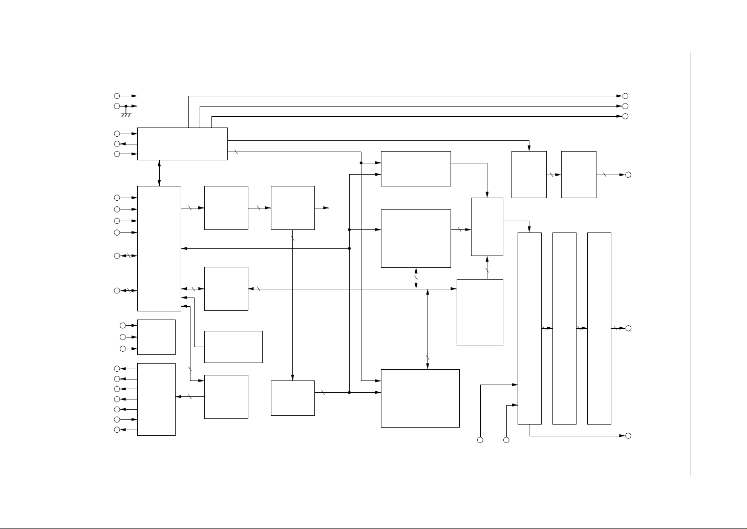
BLOCK DIAGRAM
¡ Semiconductor MSM6562B-xx
2/50
V
V
OSC
OSC
OSC
R/W
RS
RS
DB0 - DB
DB4 - DB
DD
V
V
V3'
V
V
V
V5'
L
SS
CP
DF
1
R
2
E
0
1
4
3
4
7
T
1
T
2
T
3
1
2
3
4
5
Timing
generation
circuit
Input/
output
buffer
8
Test
circuit
voltage dividing circuit
LCD bias
5
Instruction
5
Contrast
register
(IR)
Data
register
(DR)
Busy flag
(BF)
register
(CR)
7
88
Instruction
decoder
(ID)
7
Cursor blink
control
Character
generator
RAM
5
Parallel/ serial
conversion
16-bit
shift
register
COMMON
16 16
signal
driver
COM
1 - 16
(CG RAM)
8
8
5
Character generator
ROM (CG ROM)
100-bit shift register
100-bit latch
100
100
SEGMENT signal driver
100
SEG
1 - 100
8
Address
counter
(ADC)
7
Display data
RAM
(DD RAM)
DO
SHL
SHL
0
1
¡ Semiconductor MSM6562B-xx
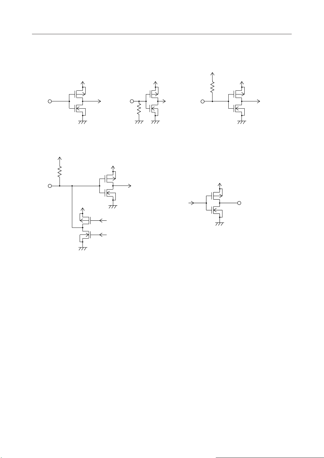
INPUT AND OUTPUT CONFIGURATION
V
DD
V
DD
V
DD
V
DD
P
N
Applied to Pin E. Applied to Pins R/W, RS0 and RS1.
V
DD
Applied to Pins T1, T2 and T3.
V
DD
P
N
V
DD
P
N
Applied to DB
- DB7.
0
P
N
V
DD
P
N
Applied to DO, CP, L and DF.
P
N
3/50
¡ Semiconductor MSM6562B-xx
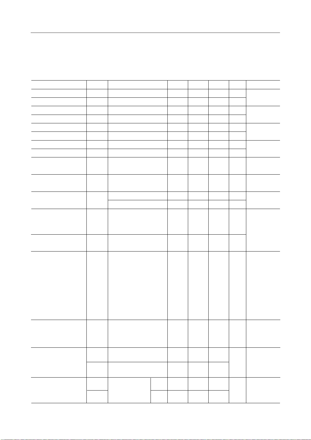
PIN DESCRIPTIONS
Symbol Description
R/W
RS0, RS
1
E
- DB
DB
0
7
OSC1, OSC2,
OSC
R
COM1 - COM
SEG1 - SEG
SHL0, SHL
100
1
DO Data output pin to send serial data to the character extension IC.
CP Clock output pin to transfer the serial data to the character extension IC.
L Latch output pin to latch the transferred data to the character extension IC.
DF Output pin for the alternating signal (DF, display frequency) required for an LCD display.
V
DD
V
SS
V1 - V5, V3' Bias voltage input pins to drive an LCD and bias setting pin. (Built-in bias dividing resistor)
V5' Contrast adjusting voltage output pin.
Read/write selection input pin.
"H": Read, and "L": Write
Register selection input pins.
RS0 "H" RS1 "H": Data register
RS0 "L" RS1 "H": Instruction register
RS0 "L" RS1 "L": Contrast register
Input pin for data input/output between CPU and MSM6562B-xx and for activating
instruction.
Input/output pins for data send/receive between CPU and MSM6562B-xx.
Clock oscillating pins required for internal operation upon receipt of CPU instruction and
the LCD drive signal.
When oscillated by an external resistor, connect a resistor between OSC
When oscillated by a built-in resistor, connect OSC
LCD COMMON signal output pins.
16
and OSC2 externally.
R
LCD SEGMENT signal output pins.
Input pins to control the transfer direction of the SEGMENT signal output data. See table below.
Power supply pin.
Ground pin.
1/4 bias : Connect V
1/5 bias : Connect V
Since V
V
SS
value depends on V5 voltage, connect a variable resistor between V5 pin and
LCD
potential or connect V5 pin and V5' pin to adjust V
and V3. Leave V3' open.
2
and V3'.
3
LCD
.
and OSC2.
1
SHL
SHL
0
1
LL
LH
HL
HH
Segment data transfer direction
SEG1ÆSEG
SEG
100
ÆSEG
100
1
SEG1ÆSEG50fiSEG
SEG
ÆSEG
100
1
100
ÆSEG
51
4/50
¡ Semiconductor MSM6562B-xx
ABSOLUTE MAXIMUM RATINGS
Parameter
Supply voltage
Supply voltage for LCD
display
Input voltage
Junction temperature
Storage temperature
Symbol
V
DD
V1, V2, V3,
, V
V
4
5
V
I
T
j
T
STG
Condition
Ta = 25°C
Ta = 25°C
Ta = 25°C
—
—
RECOMMENDED OPERATING CONDITIONS
Parameter
Supply voltage
LCD driving voltage
Operating temperature
*1 This voltage should be applied to VDD – V5.
Voltages applicable to V1, V2, V3 and V4 are as follows:
V1 = VDD – 1/4 (VDD – V5)
V2 = V3 = VDD – 1/2 (VDD – V5)
V4 = VDD – 3/4 (VDD – V5)
Symbol
V
DD
V
LCD
op
Condition
– V
V
DD
VDD – V
—
1/4 bias
SS
1/5 bias
SS
—T
*
*
1
2
Rating
–0.3 to + 7.0
–0.3 to V
–0.3 to V
150
–55 to + 150
Range
4.5 to 5.5
3.0 to 5.5
3.0 to 5.5
–30 to +85
DD
DD
+ 0.3
+ 0.3
3
*
3
*
Unit
V
V
V
°C
°C
Unit
V
V
V
°C
Applicable Pin
VDD, V
SS
V
, V2, V3,
1
, V
V
4
5
R / W, RS1,
, E,
RS
0
- DB
DB
0
7
OSC
1
—
—
Applicable Pin
VDD, V
SS
, V
V
DD
5
—
*2 This voltage should be applied to VDD – V5.
Voltages applicable to V1, V2, V3 and V4 are as follows:
V1 = VDD – 1/5 (VDD – V5)
V2 = VDD – 2/5 (VDD – V5)
V3 = VDD – 3/5 (VDD – V5)
V4 = VDD – 4/5 (VDD – V5)
*3 The relation of VDD > V1 > V
≥ V
(=V3') > V4 > V
2
3
(High ¨Æ Low)
LCD driving voltage can be adjusted by varying V5.
However, V5 cannot be used under VSS voltage.
≥ V
5
must be kept.
SS
5/50
¡ Semiconductor MSM6562B-xx
ELECTRICAL CHARACTERISTICS
DC Characteristics
(VDD = 4.5 to 5.5V, Ta = -30 to +85°C)
Parameter
"H" input voltage
"H" input voltage
"L" input voltage
"H" output voltage
"L" output voltage
"H" output voltage
"L" output voltage
COM voltage drop
Symbol
V
IH1
IL1
V
IH2
V
IL2
V
OH1
V
OL1
V
OH2
V
OL2
V
C
Condition
I
= –0.205mA
O
= 1.6mA
I
O
= –40mA
I
O
= 40mA
I
O
I
= ± 40mA
O
(Note 1)
—
Min.
2.2
Typ.—Max.
V
— –0.3 — 0.6
—
—
V
0.9V
DD
– 0.8
–0.3
2.4
—
—
—
DD
—V
—
—
—
—
—
—
0.8
—
0.4
—
0.1V
2.3
DD
DD
DD
Unit
V
V"L" input voltage V
V
V
V
V
V
V
V
Applied Pin
R/W, RS
0
DB0 - DB
OSC
SHL0, SHL
DB0 - DB
DO, CP, L,
DF, OSC
COM1 - COM
, RS1, E,
7
1
1
7
2
16
SEG voltage drop
Input leakage current
"H" input current
"L" input current I
Supply current
LCD driving bias
resistance
Variable range by built-in
variable resistor for LCD
driving voltage
V
S
I
IL
I
IH2
IO = ± 40mA
(Note 1)
= V
V
I
DD
VI = V
SS
VI = V
DD
Except the current flowing
to the pull-up resistor and
output driving MOS.
VDD = 5.0V
IL2
I
DD
LBR kW
V
LCD MAX
V
LCD MIN
= V
V
I
SS
V
= 5.0V
DD
E = "L" level, SHL
Built-in R
clock input to OSC
External clock frequency (f
270kHz.
R/W, RS
open.
Output pins are all no load. Except
bias current for LCD driving.
(Note 2, 3, 4)
, SHL1 = "L" level
0
oscillation or external
f
.
1
) is
IN
, RS1, and DB0 to DB7 are
0
—
V
= 5.0V, 1/5 bias
DD
VDD = 5.0V, 1/5 bias
—
—
—
—
—
—
3.0
1
–1
—— 2mA
–34
–83
–204
—— 1
248
4.6 — —
— — 3.7
V
mA
mA
mA
mA
V
SEG1 - SEG
E, SHL0, SHL
R/W, RS0, RS1,
VDD – V1, V1 – V
V2 – V3', V3 – V
V
DD
DB0 - DB
V
DD
V4 – V
– V5 (V5')
100
7
5
1
2
4
LCD driving bias voltage
(external input)
V
V
LCD1
LCD2
– V
V
DD
(Note 5)
5
1/5 bias
1/4 bias
3.0 — 5.5
3.0 — 5.5
V
VDD, V1, V2, V3,
V
', V
, V
3
4
5
6/50
¡ Semiconductor MSM6562B-xx
(Note 1) Applies to the voltage drop (VC) from VDD, V1, V4 and V5 to each COMMON pin
(COM1 to COM16) as well as to voltage drop (VS) from VDD, V2, V3 and V5 to each
SEG pin (SEG1 to SEG
) when 40mA is flowed through one COM or SEG pin.
100
When output level is at VDD, V1, or V2 level, 40mA is flowed out, while 40mA is
flowed in when the output level is at V3, V4 or V5 level.
This occurs when 5V is input to VDD, V1 and V2 , and 0V is input to V3, V4 and
V5.
(Note 2) Applies to the current value flowed in the pin VDD, in the case of VDD = 5V,
VSS = 0V, V1, V2 = 5V, V3, V4, V5 = 0V and V5' is open.
(Note 3) Built-in Rf oscillation circuit
OSC
1
Minimum wiring is required between OSCR and OSC2.
OSC
OSC
R
2
Leave OSC1 open.
(Note 4) External clock input circuit
Input pulse
OSC
OSC
OSC
1
R
2
Leave OSCR and OSC2 open.
(Note 5) Input the voltage to V5. (However, V5 cannot be used under VSS voltage.)
N (number of LCD lines)
Pin
V
1
V
2
V
3
V
4
V
5
1-line mode
Bias : 1/4
V
LCD
VDD –
4
V
LCD
VDD –
2
V
LCD
VDD –
2
3V
VDD – V
LCD
4
LCD
VDD –
2-line mode
Bias : 1/5
V
LCD
VDD –
5
2V
VDD – V
LCD
5
3V
LCD
5
4V
LCD
5
LCD
VDD –
VDD –
VDD –
At 1/4 bias : Connect V2 and V3 externally and leave V3' open.
At 1/5 bias : Connect V3 and V3' externally.
V
is the LCD driving voltage. (For N [number of LCD lines], refer to
LCD
the explanation of the Function setting instruction of the instruction code.)
7/50
¡ Semiconductor MSM6562B-xx
y
AC Characteristics
Parameter Symbol Condition Unit
R
= 120 kW ± 2%
Rf clock oscillation
frequency
f
External clock frequency f
External clock duty f
External clock rise time t
External clock fall time t
Built-in Rf clock
oscillation frequency
f
OSC1
IN
duty
rf
ff
OSC2
f
(Note 1)
OSC
and OSC2 are open.
R
Input a pulse to OSC
(Note 4)
(Note 2)
(Note 3)
(Note 3)
OSC
is open.
1
Connect OSC
(Note 5)
and OSC2.
R
(Note 1)
OSC
OSC
OSC
1
R
R
2
f
Minimum wiring is required between OSC1 and Rf and
between OSC2 and Rf.
Leave OSCR open.
Min. Typ. Max.
.
1
R
= 120kW ± 2%
f
Applicable Pin
kHz175 270 350
kHz125 — 480
%45 50 55
ms— — 0.2
ms— — 0.2
kHz140 280 480
OSC
OSC
OSC
OSC
OSC
OSC
OSC
OSC
OSC
1
2
1
1
1
1
1
R
2
(Note 2)
t
HW
V
DD
f
IN
2
V
DD
2
waveform
f
= t
dut
/(tHW + tLW) ¥ 100 (%)
HW
(Note 3) Applies to the pulse to be input to OSC
V
– 0.8V
DD
f
IN
0.8V
V
– 0.8V
DD
0.8V
waveform
t
rf
t
ff
(Note 4) See Note 4 to "DC Characteristics."
t
LW
Applies to the pulse to be
input to OSC
V
DD
1
2
.
1
Applies to the pulse to be
input to OSC
1
(Note 5) See Note 3 to "DC Characteristics."
8/50
¡ Semiconductor MSM6562B-xx
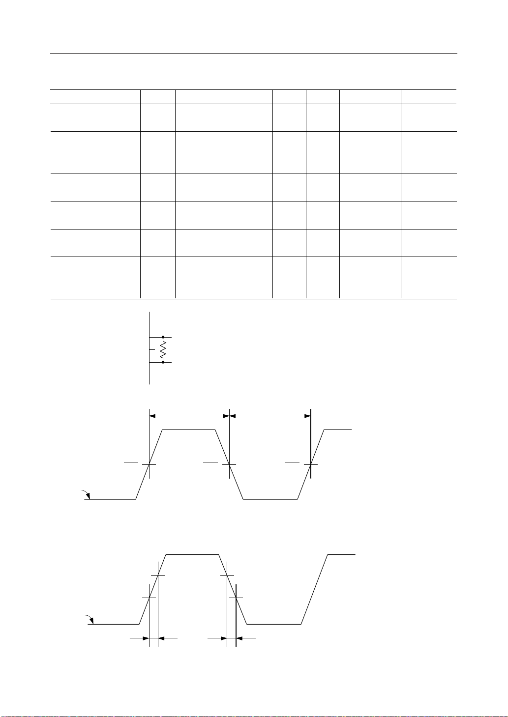
Switching Characteristics
1. Timing for input from the CPU (write operation)
= 4.5 to 5.5V, Ta = –30 to +85°C)
(V
DD
Parameter Symbol
R/W, RS0 and RS1 setup time
E "H" pulse width
R/W, RS
and RS1 hold time
0
E rise time
E fall time
E "L" pulse width
E cycle time
DB
to DB7 input data setup time
0
DB
to DB7 input data hold time
0
RS1,
0
R/W
E
Min. Typ. Max. Unit
t
B
t
W
t
A
t
r
t
f
t
L
t
C
t
I
t
H
V
IH1
V
IL1
V
IL1
t
B
t
L
V
IL1
V
IL1
40
220
10
—
—
210
500
100
10
t
r
V
IH1
—
—
—
—
—
—
—
—
—
t
t
W
f
V
IH1
t
I
—
—
—
20
20
—
—
—
—
V
IH1
V
IL1
V
IL1
t
A
V
IL1
t
H
ns
ns
ns
ns
ns
ns
ns
ns
ns
DB
0-7
V
IH1
Input data
V
IL1
t
c
V
IH1
V
IL1
9/50
¡ Semiconductor MSM6562B-xx
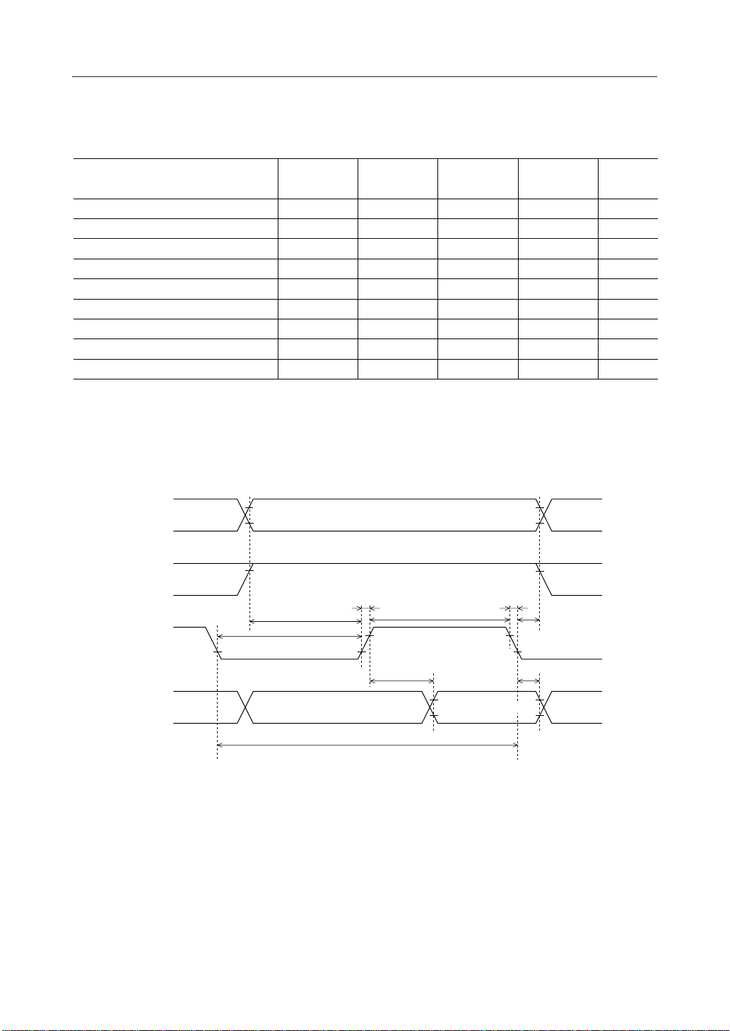
2. Timing for output to the CPU (read operation)
= 4.5 to 5.5V, Ta = –30 to +85°C)
(V
DD
Parameter Symbol
R/W, RS0 and RS1 setup time
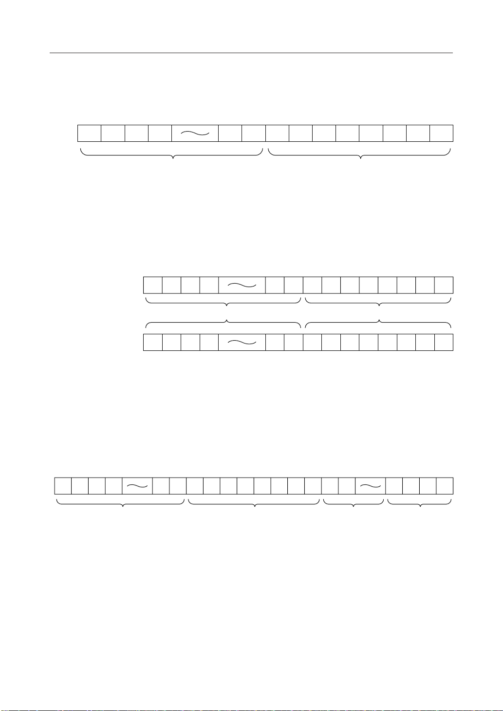
E "H" pulse width
R/W, RS
and RS1 hold time
0
E rise time
E fall time
E "L" pulse width
E cycle time
DB
to DB7 data ouput delay time
0
DB
to DB7 data ouput hold time
0
RS1,
0
R/W
Min. Typ. Max. Unit
t
B
t
W
t
A
t
r
t
f
t
L
t
C
t
D
t
O
V
IH1
V
IL1
V
IL1
40
220
10
—
—
210
500
—
20
—
—
—
—
—
—
—
—
—
—
—
—
20
20
—
—
150
—
V
IH1
V
IL1
V
IL1
ns
ns
ns
ns
ns
ns
ns
ns
ns
DB
t
t
B
t
E
0-7
V
IL1
L
V
IL1
r
V
IL1
t
c
t
W
t
D
V
OH1
V
OL1
t
f
V
IH1
Output data
t
A
V
IL1
t
O
V
OH1
V
OL1
10/50
¡ Semiconductor MSM6562B-xx
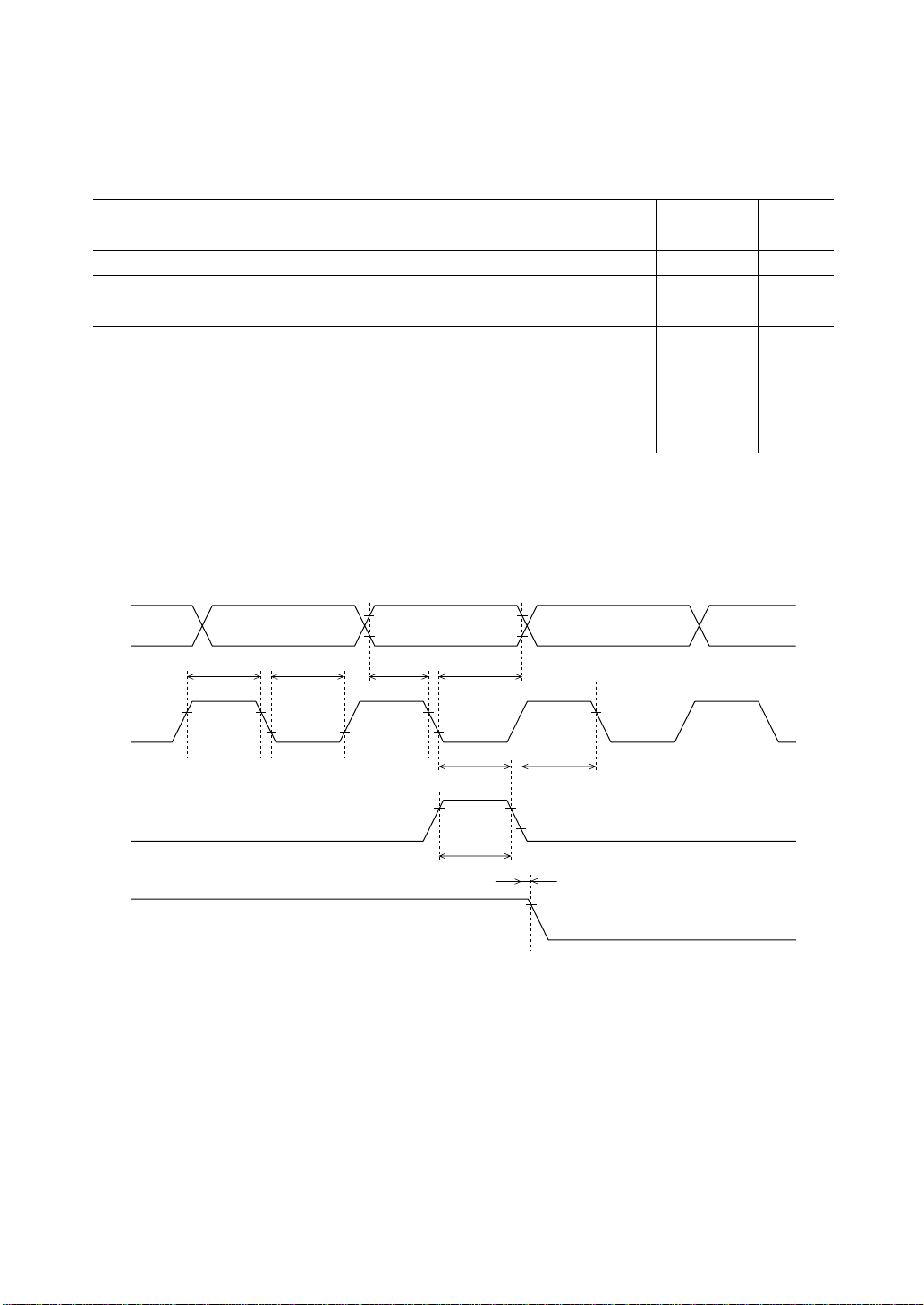
3. Timing for output to character extension IC
(V
= 4.5 to 5.5V, Ta = –30 to +85°C)
DD
Parameter Symbol
CP "H" pulse width
CP "L" pulse width
DO setup time
DO hold time
L clock setup time
L clock hold time
L "H" pulse width
DF delay time
DO
V
OH2
CP
t
HW1
Min. Typ. Max. Unit
t
HW1
t
LW
t
S
t
DH
t
SU
t
HO
t
HW2
t
M
V
OH2
V
OL2
t
LW
V
OH2
V
OL2
t
S
V
OH2
V
OL2
800
800
300
300
500
100
800
–1000
V
OH2
V
OH2
t
DH
V
OL2
t
SU
—
—
—
—
—
—
—
—
V
OH2
t
HO
—
—
—
—
—
—
—
1000
ns
ns
ns
ns
ns
ns
ns
ns
L
DF
V
OH2
t
HW2
V
OH2
V
OL2
t
M
V
OH2
11/50
¡ Semiconductor MSM6562B-xx
FUNCTIONAL DESCRIPTION
1. Instruction Register (IR), Data Register (DR), Contrast Register (CR)
These three registers are selected by the register selector pins, RS0 and RS1.
When RS0 and RS1 are "H" level input, the DR is selected and when RS0 = "L" level input and RS
= "H", the IR is selected. On the other hand, when RS0 and RS1 are "L" level input, the CR is
selected. (When RS0 = "H" level input and RS1 = "L", the registers are ignored.)
The IR is used to store the address codes for the display data RAM (DD RAM) or character
generator RAM (CG RAM) and instruction codes.
The IR can be written into, but not be read out by the microcomputer (CPU).
The CR can be used to read out and write. The CR values provide 0 to 1F (hexadecimal) and when
this value is 0, V
1F.) Therefore, the contrast can be adjusted by varying the CR value (providing that V5 and V5'
are connected).
The DR is used to write into/read out the data to/from the DD RAM or CG RAM.
The data written to the DR by the CPU is automatically written to the DD RAM or CG RAM as
an internal operation.
When an address code is written to the IR, the data (of the specified address) is automatically
transferred from the DD RAM or CG RAM to the DR. By having the CPU subsequently read the
DR (from the DR data), it is possible to verify the DD RAM or CG RAM data.
After the writing of the DR by the CPU, the DD RAM or CG RAM of the next address is selected
to be ready for the next CPU writing. Likewise, after the reading out of the DR by the CPU, the
DD RAM or CG RAM data is read out by the DR to be ready for the next CPU reading.
Write/read to and from the three registers is carried out by the READ/WRITE (R/W) pin.
is lowest. On the other hand, when it is 1F, it is highest. (The initial value is
LCD
1
Table 1 Register and R/W pins function table
R/W RS
LLH
HLH
LHH
HHH
LLL
HLL
0
RS
1
IR write
Read of busy flag (BF) and address counter (ADC)
DR write
DR read
CR write
CR read
Function
2. Busy Flag (BF)
When the busy flag output is at "H", it indicates that the MSM6562B-xx is engaged in internal
operation.
When the busy flag is at "H" level, any new instruction is ignored.
When R/W = "H", RS0 = "L", and RS1 = "H", the busy flag is output from DB7.
New instruction should be input when BF is "L" level.
When the busy flag is set to "H", the output code of the address counter (ADC) are undefined.
12/50

¡ Semiconductor MSM6562B-xx
3. Address Counter (ADC)
The address counter (ADC) allocates the address for the DD RAM and CG RAM and also for the
cursor display.
When the instruction code for the DD RAM address or CG RAM address setting is input to the
IR, after deciding whether it is the DD RAM or CG RAM, the address code is transferred from
the IR to the ADC. After writing (reading) the display data to (from) the DD RAM or CG RAM,
the ADC is automatically incremented (decremented) by 1 as its internal operation.
The data of the ADC is output to DB0 - DB6 under the conditions that R/W = "H", RS0 = "L", RS
= "H" and BF = "L".
4. Timing Generator Circuit
This circuit generates timing signals used for internal operations upon receipt of CPU instruction. It also generates timing signals for activating such internal circuits as the DD RAM, CG RAM
and CG ROM.
It is so designed that the internal operation caused by accessing from the CPU will not interfere
with the internal operation caused by the LCD display.
Consequently, when data is written from the CPU to DD RAM no ill effect, e.g., flickering occurs
in portions other than the display where the data is written.
In addition, the circuit generates transfer signals to the character extension IC (MSM5259).
1
13/50
¡ Semiconductor MSM6562B-xx
5. Display Data RAM (DD RAM)
This RAM is used to store the display data of 8-bit character codes (see Table 2).
DD RAM address corresponds to the display position of the LCD. The correspondence between
the two is described in the following.
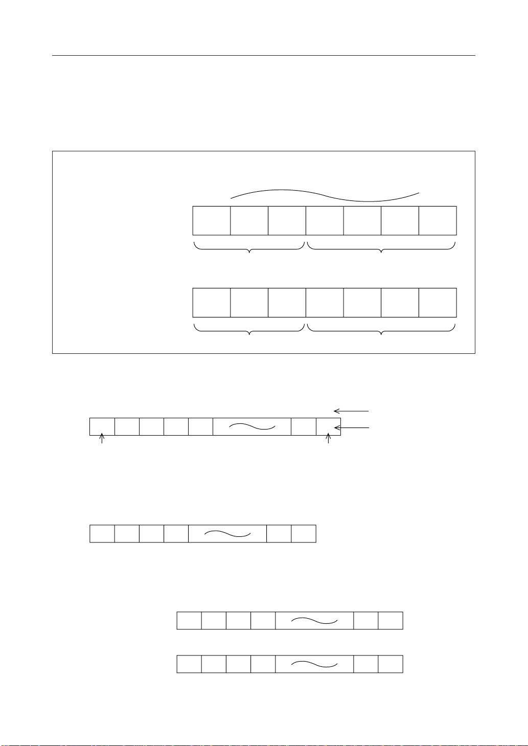
DD RAM address (set to ADC) is expressed in hexadecimal notation as shown below:
ADC
(Example)
When DD RAM address
is 2A
DB
6
MSB LSB
Hexadecimal notation
LLHLHLH
2
Hexadecimal notation
A
DB
0
1-1) Correspondence between address and display position in the 1-line display mode
79 80First digit 2345
00 01 02 03 04 4E 4F
MSB LSB
Display position
DD RAM address (hex.)
1-2) When the MSM6562B-xx alone is used, up to 20 characters can be displayed from the
first digit to the twentieth digit.
19 20First digit 2 3 4
00 01 02 03 12 13
When the display is shifted by instruction, the correspondence between the LCD
display position and the DD RAM address changes as shown below:
19 20First digit 2 3 4
(Display shifted to right)
(Display shifted to left)
4F 00 01 02 11 12
19 20First digit 2 3 4
01 02 03 04 13 14
14/50
¡ Semiconductor MSM6562B-xx
1-3) When the MSM6562B-xx is used with one MSM5259, up to 28 characters can be
displayed from the first digit to the twenty-eighth digit as shown below:
00 01 02 03 12 13
When the display is shifted by instruction, the correspondence between the
LCD display and DD RAM address changes as shown below:
(Display shifted to right)
(Display shifted to left)
19 20First digit 2 3 4
1421152216231724182519261A271B
MSM6562B-xx display
19 20First digit 2 3 4
4F 00 01 02 11 12 13 14 15 16 17 18 19 1A
MSM6562B-xx display
01 02 03 04 13 14 15 16 17 18 19 1A 1B 1C
MSM5259 display
21 22 23 24 25 26 27 28
MSM5259 display
28
1-4) Since the MSM6562B-xx has a DD RAM with a capacity of 80 characters, up to 8 devices
of MSM5259 can be connected to MSM6562B-xx so that 80 characters can be displayed.
First
digit 2 3 4
00 01 02 03 12 13
MSM6562B-xx display
19 20
28
1421152216231724182519261A271B
MSM5259 (1) display
29 30 77 78 79 80
1C 1D 4C 4D 4E 4F
MSM5259
(2)-(7) display
i.e., O
MSM5259
(8) display
(Only the half of the
segment output pins,
to O20, are used.)
1
15/50

¡ Semiconductor MSM6562B-xx
2-1) Correspondence between address and display position in the 2-line display mode
39 40First digit 2345 Display position
First line
00 01 02 03 04 26 27
DD RAM address (hex.)
Second line
40 41 42 43 44 66 67
(Note) Note that the last address of the first line and the leading address of the
second line are not consecutive.
2-2) When the MSM6562B-xx alone is used, up to 40 characters (20 character ¥ 2 lines) can
be displayed from the first digit to the twentieth digit.
19 20First digit 2 3 4
First line
Second line
00 01 02 03 12 13
40 41 42 43 52 53
When the display is shifted by instruction, the correspondence between the LCD
display position and the DD RAM address changes as shown below:
19 20First digit 2 3 4
(Display shifted to right)
First line
Second line
27 00 01 02 11 12
67 40 41 42 51 52
19 20First digit 2 3 4
(Display shifted to left)
First line
Second line
01 02 03 04 13 14
41 42 43 44 53 54
2-3) When the MSM6562B-xx is used with one MSM5259, up to 56 characters (28 characters
¥ 2 lines) can be displayed from the first digit to the twenty-eighth digit as shown
below:
First line
Second line
19 20First digit 2 3 4
00 01 02 03 12 13
40 41 42 43 52 53
MSM6562B-xx display
21
14
54
22
23
15
16
55
56
MSM5259 display
24
17
57
25
18
58
26
19
59
27
1A
5A
28
1B
5B
16/50

¡ Semiconductor MSM6562B-xx
When the display is shifted by instruction, the correspondence between the LCD
display position and the DD RAM address changes as shown below:
(Display shifted to right)
First line
Second line
(Display shifted to left)
First line
Second line
27 00 01 02 11 12
67 40 41 42 51 52
01 02 03 04 13 14
41 42 43 44 53 54
19 20First digit 2 3 4
MSM6562B-xx display
19 20First digit 2 3 4
MSM6562B-xx display
21
13
53
21
15
55
22
23
14
15
54
55
MSM5259 display
22
23
16
17
56
57
MSM5259 display
24
16
56
24
18
58
25
17
57
25
19
59
26
18
58
26
1A
5A
27
19
59
27
1B
5B
2-4) Since the MSM6562B-xx has a DD RAM with a capacity of 80 characters, up to 3 devices
of MSM5259 can be connected to the MSM6562B-xx in the 2-line display mode.
First
digit
234
00 01 02 03 12 13
40 41 42 43 52 53 54 55 56 57 58 59 5A 5B 5C 5D 64 65 66 67
19 20
1421152216231724182519261A271B
28
29 30 37 38 39 40
1C 1D 24 25 26 27
28
1A
5A
28
1C
5C
MSM6562B display
MSM5259 (1) display
MSM5259
(2) display
(Only the half of the segment
output pins, i.e., O
1
MSM5259
(3) display
to O20, are used.)
6. Character Generator ROM (CG ROM)
The CG ROM is used to generate 5 ¥ 7 dot (160 kinds) character patterns or 5 ¥ 10 dot (32 kinds)
character patterns from an 8-bit DD RAM character code signal.
The correspondence of 8-bit character codes to character patterns is shown in Table 2.
When the 8-bit character code of the CG ROM is written to the DD RAM, the character pattern
of the CG ROM corresponding to the code is displayed on the LCD display position corresponding to the DD RAM address.
17/50

¡ Semiconductor MSM6562B-xx
Lower
4 bits
0000
LSB
0001
0010
0011
0100
0101
0110
0111
1000
1001
1010
1011
Upper
4 bits
MSB
0000 0010 0011 0100 0101 0110 0111 1010 1011 1100 1101 1110 1111
CG
RAM (1)
(2)
(3)
(4)
(5)
(6)
(7)
(8)
(1)
(2)
(3)
(4)
0
!
1
2
#
$
%
&
3
4
5
6
7
(
)
*
+
8
9
:
;
@
A
B
C
D
E
F
G
H
I
J
K
P
Q
R
S
T
U
V
W
X
Y
Z
[
/
a
b
c
d
e
f
n
h
i
j
k
p
q
r
s
t
u
v
w
x
y
z
{
a
ä
b
e
m
s
r
g
√
–1
j
x
Table 2 Character codes and character patterns of standard code (MSM6562B-01)
R
q
Q
•
W
ü
S
p
X
18/50
1100
1101
1110
1111
(5)
(9)
(7)
(8)
¢
£
÷
n
ö
Æ
¨
Ù
}
°
<
–
.
/
=
>
?
L
M
N
O
¥
]
^
_
l
m
n
o

¡ Semiconductor MSM6562B-xx
7. Character Generator RAM (CG RAM)
The CG RAM is used to display user's original character patterns other than those stored in the
CG ROM.
The CG RAM has the capacity (64 bytes = 512 bits) to write 8 kinds for 5 ¥ 7 dots or 4 kinds for
5 ¥ 10 dots.
When displaying character patterns stored in the CG RAM, write 8-bit character codes (00 to 07
or 08 to 0F; hex.) shown on the left in Table 2 to the DD RAM. It is then possible to output the
character pattern to the LCD display position corresponding to the DD RAM address.
The following is a description on how to write and read character patterns to and from the CG
RAM.
(1) When the character pattern is 5 ¥ 7 dots (see Table 3)
• Method of writing character pattern into the CG RAM by the CPU :
The CG RAM address bits 0 to 2 correspond to the line position of the character pattern.
First, set increment or decrement by the CPU, and then input the CG RAM address.
After this, write character pattern into the CG RAM through DB0 to DB7 line by line.
DB0 to DB7 correspond to the CG RAM data bits 0 to 7 in Table 3.
The display of the character pattern is turned on when "H" is set as input data, while it is
turned off when "L" is set as the input data.
Since the ADC is automatically incremented or decremented by 1 after writing the data
to the CG RAM, it is not necessary to set the CG RAM address again.
When performing a cursor indication, set to "0" all the input data for the line the CG RAM
address bits 0 to 2 of which are all "1".
Although the CG RAM data bits 0 ~ 4 are output to the LCD as display data, the CG RAM
data bits 5 ~ 7 are not. It is possible, however, to use the CG RAM as a data RAM.
• Method of displaying the CG RAM character pattern to the LCD :
The CG RAM is selected when high-order 4 bits of the character code are all "L".
Since bit 3 of the character code is invalid, the display of "0" in Table 3 is selected by
character code "00" or "08" (hex.). When the 8-bit character code of the CG RAM is written
to the DD RAM, the character pattern of the CG RAM is displayed on the LCD display
position corresponding to the DD RAM address. (DD RAM data bits 0 to 2 correspond to
CG RAM address bits 3 to 5.)
19/50

¡ Semiconductor MSM6562B-xx
(2) When the character pattern is 5 ¥ 10 dots (see Table 4).
• Method of writing character pattern into the CG RAM by the CPU :
The CG RAM address bits 0 to 3 correspond to the line position of the character pattern.
First, set increment or decrement by the CPU, and then input the CG RAM address.
After this, write the character pattern into the CG RAM through DB0 to DB7 line by line.
DB0 to DB7 correspond to the CG RAM data bits 0 to 7, in Table 4.
The display of the character pattern is turned on when "H" is set as the input data, while
it is turned off when "L" is set as the input data.
Since the ADC is automatically incremented or decremented by 1 after writing the data
to the CG RAM, it is not necessary to set the CG RAM address again.
When performing a cursor indication, set to "0" all the input data for the line the CG RAM
address bits 0 to 2 are all "1".
CG RAM data is displayed on the LCD when the CG RAM data ranges from CG RAM data
bits 0 to 4 and the CG RAM addresses (address bits 0 to 3) are "0" to "A" (hex.). Other CG
RAM data is not displayed on the LCD (that is, when the CG RAM data ranges from CG
RAM data bits 5 to 7 and the CG RAM addresses (address bits 0 to 3) are "B" to "F" (hex.)).
It is possible, however, to read such CG RAM data through DB0 to DB7.
• Method of displaying the CG RAM character pattern to the LCD :
The CG RAM is selected when high-order 4 bits of the character code are all "L".
Since bits 0 and 3 of the character code are invalid, the display of "b" in Table 4 is selected
by character codes "00", "01", "08" and "09" (hex.).
When the 8-bit character code of the CG RAM character code is written to the DD RAM,the
character pattern of the CG RAM is displayed on the LCD display position corresponding
to the DD RAM address.
(DD RAM data bits 1 to 2 correspond to CG RAM address bits 4 to 5.)
20/50

¡ Semiconductor MSM6562B-xx
,
Table 3 Example of the CG RAM data (character pattern) corresponding to the CG RAM
addresses when the character pattern is 5 ¥ 7 dots, and relationship between character
patterns and the DD RAM data
CG RAM address
CG RAM data
(character pattern)
543210 76543210
MSB LSB MSB LSB
000000
001
010
011
100
101
110
111
001000
001
010
011
100
101
110
111
111000
001
010
011
100
101
110
111
XXX011
100
100
100
100
100
011
000
XXX100
100
101
110
101
100
100
000
XXX011
001
001
001
001
001
011
000
1
0
0
0
0
0
1
0
0
1
0
0
0
1
0
0
1
0
0
0
0
0
1
0
DD RAM data
(character code)
65432107
MSB LSB
0
1
1
1
1
000 0X000
1
0
0
1
0
0
0
0
000 0X001
0
1
0
0
0
0
0
0
000 0X111
0
0
0
X : Don't Care
21/50

¡ Semiconductor MSM6562B-xx
,
,
,
Table 4 Example of the CG RAM data (character pattern) corresponding to the CG RAM
addresses when the character pattern is 5 ¥ 10 dots, and relationship between
character patterns and the DD RAM data
CG RAM address
543210 765 43210
MSB LSB MSB LSB
000000
001
0
010
0
011
0
100
0
101
0
110
0
111
0
000
1
001
1
010
1
011
1
100
1
101
1
110
1
111
1
000000
001
0
010
0
011
0
100
0
101
0
110
0
111
0
000
1
001
1
010
1
011
1
100
1
101
1
110
1
111
1
CG RAM data
(character pattern)
XXX000
000
011
100
111
100
111
100
100
100
000
XXX
XXX000
000
011
100
100
100
011
000
000
011
000
XXX
0
0
1
0
1
0
1
0
0
0
0
X
0
0
1
0
0
0
1
0
0
1
0
X
DD RAM data
(character code)
65432107
MSB LSB
0
0
0
1
0
000 0 X 0 0 X
1
0
0
0
0
0
X
0
0
1
1
1
000 0 X 0 1 X
1
1
1
1
0
0
X
000000
001
0
010
0
011
0
100
0
101
0
110
0
111
0
000
1
001
1
010
1
011
1
100
1
101
1
110
1
111
1
X : Don't care
XXX000
000
110
010
100
100
011
000
000
000
000
XXX
0
0
0
0
1
1
1
0
0
1
0
1
1
0
0
0
0
0
0
0
0
0
X
X
000 0 X 1 1 X
22/50

¡ Semiconductor MSM6562B-xx
8. Cursor and Blink Control Circuit
This circuit generates the LCD cursor and blink.
This circuit is under the control of the CPU program. The display of the cursor or blink on the LCD
is made at a position corresponding to the DD RAM address set to the ADC.
The figure below shows an example of the cursor and blink position when the value of the ADC
is set at "07" (hex.).
In 1-line display mode 06707808
In 2-line display mode
First line
Second line
DB
6
LLLADC
0
00 01 02 03 04 05
00 01 02 03 04 05
40 41 42 43 44 45 46 47 48 66 67
L H HH
56First digit 2 3 4
56First digit 2 3 4
7
DB
0
06707808
9
4E794F
Cursor and blink position
9
263927
Cursor and blink position
80
40
(Note) The cursor and blink are displayed even when the CG RAM address is set to the ADC.
For this reason, it is necessary to inhibit the display of the cursor and blink while the
CG RAM address is set to the ADC.
23/50

¡ Semiconductor MSM6562B-xx
9. LCD Display Circuit (COM1 to COM16, SEG1 to SEG
, L, CP, DO, DF, SHL0, SHL1) :
100
Since the MSM6562B-xx provides the COM signal outputs (16 outputs) and the SEG signal
outputs (100 outputs), even a single MSM6562B-xx device can display 20 characters (1-line
display) or 40 characters (2-line display).
The character pattern data is converted into the serial data and is serially transferred through the
shift register. The transfer direction of the serial data is controlled by SHL0 and SHL1 and is
shown as follows.
SHL
LL
LH
HL
HH
SHL
0
1
SEG1ÆSEG
SEG
100
SEG1ÆSEG50fiSEG
SEG
100
ÆSEG
ÆSEG
Transfer direction
100
1
ÆSEG
100
1
51
Connect SHL0 and SHL1 to VDD or VSS. Keep the set states of the SHL0 and SHL1 pins unchanged
during IC operation.
The SEG1 to SEG
are used to display 20-digit display on the LCD. To display more than 20
100
digits, the character extension IC (MSM5259) is used.
The character extension IC (MSM5259) is an extended IC for segment signal output. Interfacing
with the MSM5259 is provided through data output pin (DO), clock output pin (CP), latch output
pin (L), and display frequency pin (DF). The character pattern data is serially transferred to the
MSM5259 through DO and CP. When 60-character (= 1-line display) or 20-character (= 2-line
display) is output, the latch pulse is also output through pin L. By this latch pulse, the data
transferred serially to the MSM5259 is latched to be used as the display data. The display
frequency (DF) signal required when the LCD is displayed is also output from DF pin in
synchronization with this latch pulse.
24/50

¡ Semiconductor MSM6562B-xx
10. Built-in Reset Circuit
The MSM6562B-xx is automatically initialized when the power is turned on.
During initialization, the busy flag (BF) holds "H" and does not accept instructions (other than
the busy flag read).
The busy flag goes to "H" for 15 ms after VDD reaches 4.5V or more.
During initialization, the MSM6562B-xx executes the following instructions :
• Display clear
• Data length of interface with CPU : 8 bits (8B/4B = "H")
• LCD : 1-line display (N = "L")
• Character font : 5 ¥ 7 dots (F = "L")
• ADC : increment (I/D = "H")
• No display shift (S = "L")
• Display : Off (D = "L")
• Cursor : Off (C = "L")
• No blink (B = "L")
• Contrast data : 1F (hex.) set
When the built-in reset circuit is used, the power supply conditions shown in the figure below
must be satisfied. If they are not satisfied, because in that case the built-in reset circuit does not
operate normally, initialize the MSM6562B-xx by instruction through the CPU (see the section
on instruction initialization).
If a battery is used as supply voltage source, be sure to initialize the instruction.
4.5V
0.2V
V
DD
t
ON
0.1ms £ t
£ 100ms 1ms £ t
ON
Power ON/OFF waveform
0.2V 0.2V
t
OFF
OFF
25/50

¡ Semiconductor MSM6562B-xx
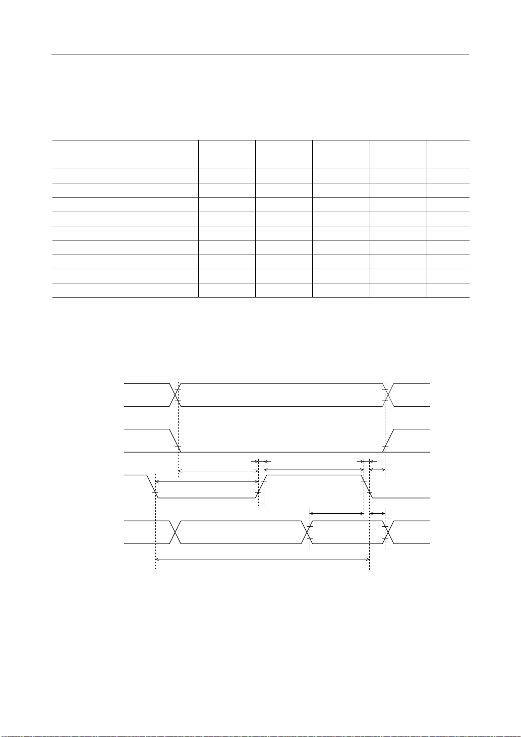
11. Data Bus with CPU
The MSM6562B-xx has either a one-step access in 8 bits or a two-step access in 4 bits to execute
an instruction so that the MSM6562B-xx can interface with both an 8-bit CPU and a 4-bit CPU.
(1) When the interface data length is 8 bits
Data buses DB0 to DB7 (8 lines) are all used and data input/output is carried out in one
step.
(2) When the interface data length is 4 bits
The 8-bit data input/output is carried out in two steps by using only high-order 4 bits of
data buses DB4 to DB7 (4 lines).
The first time data input/output is made for high-order 4 bits (DB4 to DB7 when the
interfaces data length is 8 bits) and the second time data input/output is made for loworder 4 bits (DB0 to DB3 when the interface data length is 8 bits). Even when the data
input/output can be completely made through high-order 4 bits, be sure to make another
input/output of low-order 4 bits. (Example : Busy flag read)
Since the data input/output is carried out in two steps but as one execution, no normal
data transfer is executed from the next input/output if accessed only once.
26/50

¡ Semiconductor MSM6562B-xx
RS
1
RS
0
R/W
E
Busy
(internal
operation)
DB
7
IR7
Busy
No
Busy
DR7
DB
DB
DB
DB
DB
DB
DB
6
5
4
3
2
1
0
Instruction register
IR6
IR5
IR4
IR3
IR2
IR1
IR0
(IR) write
Busy flag (BF) and
address counter (ADC) read
Example of 8-bit data transfer
ADC6
ADC5
ADC4
ADC3
ADC2
ADC1
ADC0
DR6
DR5
DR4
DR3
DR2
DR1
DR0
Data register
(DR) write
27/50

RS
1
RS
0
R/W
E
Busy
(internal operation)
DB
7
IR7
IR3
Busy
No
Busy
ADC3
DR7
¡ Semiconductor MSM6562B-xx
DR3
28/50
DB
DB
DB
DR6
DR5
DR4
Data register
(DR) write
DR2
DR1
DR0
(IR) write
IR2
IR1
IR0
ADC6
ADC5
ADC4
Busy flag (BF) and
address counter (ADC) read
ADC2
ADC1
ADC0
6
5
4
IR6
IR5
IR4
Instruction register
Example of 4-bit data transfer

¡ Semiconductor MSM6562B-xx
12. Instruction Code
• Instruction code table
Instruction
Display clear
RS1RS0R/WDB7DB6DB5DB4DB3 DB2DB1DB0
10000000001
Code
1000000001]Cursor home
100000001I/DSEntry mode setting
Display on/off control 10000001DCB
Cursor/display shift 1000001S/CR/L]]
Function setting 100001
8B/
NF]]
4B
CG RAM address setting 10001 ACG
DD RAM address setting 1001 ADD
Busy flag/address read 1 0 1 BF ADC
CG RAM/DD RAM data
write
1 1 0 WRITE DATA
Description
After all display are cleared,
address counter for DD RAM is
set to "00".
Address counter for DD RAM is set
to "00". The shifted display returns
to the position before shift. The
contents of the DD RAM are not
changed.
Direction of the cursor move and
whether display is shifted are set.
Upon data write or read, the cursor
and the display will actually be
moved and shifted.
The on/off of all display (D), the
on/off of the cursor (C) and the
blink (B) of the character at the
cursor position are set.
The cursor and display are
shifted without changing the
contents of the DD RAM.
The interface data length (8B/4B),
the display line numbers (N)
and the character font (F) are set.
The address of the CG RAM is set
and then the CG RAM data is
specified for the data for
transmission and reception.
The address of the DD RAM is set
and then the DD RAM data is
specified for the data for
transmission and reception.
The busy flag (BF) indicating that
the internal circuits are operating
and the contents of address counter
are read out.
Data is written into the DD RAM
or CG RAM
Execution Time
ƒ
=250kHz
CP=ƒOSC
1.64ms
1.64ms
40ms
40ms
40ms
40ms
40ms
40ms
1ms
40ms
CG RAM/DD RAM data
read
Contrast adjusting data
write
Contrast adjusting data
read
1 1 1 READ DATA
0000
00100010
I/D=1
:
Increment
S=1
:
Always involves display shift
S/C=1
:
Shift of display
R/L=1
:
Shift to the right
8B/4B=1
:
8 bits
N=1
:
2 lines
F=1
:
5¥10-dots
BF=1
:
Engaged in
internal operation
WRITE CONTRAST
DATA
READ CONTRAST
DATA
, I/D=0
:
, S/C=0
:
, R/L=0
:
, 8B/4B=0
:
, N=0
:
, F=0
:
, BF=0
:
Decrement
Shift of cursor
Shift to the left
4 bits
1 line
5¥7-dots
Instruction
acceptable
Data is read out from the DD RAM
or CG RAM.
The data for contrast adjustment
is written.
The data for contrast adjustment
is read.
DD RAM
:
CG RAM
ACG
ADD
ADC
Display data RAM
:
Character generator RAM
:
CG RAM address
:
DD RAM address,
corresponding to the
cursor address
:
Address counter, used for
both DD RAM and CG
RAM
40ms
40ms
40ms
When the frequency
is changed, the
execution time is
also changed.
(Example)
When
ƒ
or ƒ
=270kHz,
CP
OSC
250
40µs ¥
270
= 37µs
]: Don't Care
29/50

¡ Semiconductor MSM6562B-xx
13. Description of Instructions
The instruction code is defined as the signal through which the MSM6562B-xx is accessed by
the CPU.
The MSM6562B-xx begins operation upon receipt of the instruction code input.
As the internal processing operation of MSM6562B-xx is started with a timing that does not affect
the LCD display, the busy status continues longer than the CPU cycle time.
Under the busy status (when the busy flag is set to "H"), the MSM6562B-xx does not execute any
instructions other than the busy flag read.
Therefore, it must be confirmed before an instruction code is input from the CPU that the busy
flag is set to "L".
(1) Display clear
When this instruction is executed, the LCD display is cleared.
The I/D value for the entry mode set instruction is set to 1 (increment). The S value for the
entry mode set instruction does not change.
When the cursor and blink are being displayed, the blinking and cursor position moves
to the left end of the LCD (the left end of the first line in the 2-line display mode).
RS
RS
Instruction code
0
0
R/W0DB
0
1
1
DB
DB
DB
DB
DB
DB
7
6
5
4
3
2
0
0
0
0
0
DB
1
0
0
1
(Note) All DD RAM data goes to "20" (hex.), while the address counter (ADC) goes to
"00" (hex.) of the DD RAM address. The execution time when the OSC
oscillation frequency is 250kHz is 1.64ms (max.).
(2) Cursor home
When this instruction is executed, the cursor and blinking position move to the left end
of the LCD (to the left end of the first line in the 2-line display mode) when the cursor and
blink are being displayed.
When the display is in shift, the display returns to its original position before shifting.
RS
RS
Instruction code
0
0
R/W0DB
0
1
1
DB
DB
DB
DB
DB
7
6
5
4
3
0
0
0
0
DB
2
0
1
X : Don't Care
(Note) The address counter (ADC) goes to "00" (hex.) of the DD RAM address. The
execution time when the OSC oscillation frequency is 250kHz is 1.64ms (max.).
DB
1
0
X
30/50

¡ Semiconductor MSM6562B-xx
(3) Entry mode set
RS
RS
Instruction code
0
0
R/W0DB
0
1
1
DB
DB
DB
DB
DB
DB
I/D
DB
1
0
S
7
6
5
4
3
2
0
0
0
0
1
1 When the I/D is set, the 8-bit character code is written or read to and from the DD
RAM, the cursor and blink shift to the right by 1 character position (I/D = "H";
increment) or to the left by 1 character position (I/D = "L"; decrement).
The address counter (ADC) is incremented (I/D = "H") or decremented (I/D = "L") by
1 at this time. Even after the character pattern code is written or read to and from the
CG RAM, the address counter (ADC) is incremented (I/D = "H") or decremented (I/
D = "L") by 1.
2 When S = "H" is set, the character code is written to the DD RAM, and then the cursor
and blink stop and the entire display shifts to the left (I/D = "H") or to the right (I/D
= "L") by 1 character position.
When the character is read from the DD RAM when S = "H" is set, or when the
character pattern data is written or read to or from the CG RAM when S = "H" is set,
the entire display does not shift, but normal write/read is performed (the entire
display does not shift, but the cursor and blink shift to the right (I/D = "H") or to the
left (I/D = "L") by 1 character position).
When S = "L" is set, the display does not shift, but normal write/read is performed.
The execution time, when the OSC oscillation frequency is 250kHz, is 40ms.
(4) Display ON/OFF control
RS
RS
Instruction code
0
0
R/W0DB
0
1
1
DB
DB
DB
DB
DB
7
6
5
4
3
0
0
0
1
DB
2
D
C
1 The D bit controls whether the character pattern is displayed or not.
When D is "H", this bit makes the character pattern display on the LCD.
When D is "L", this bit makes the display of the character pattern turned off. The cursor
and blink are also cancelled at this time.
(Note) Different from the display clear, the DD RAM data is absolutely not
rewritten.
2 The cursor goes off when C = "L" and it is displayed when D = "H" and C = "H".
3 A blink is cancelled when B = "L" and a blink is executed when D = "H" and B = "H".
In the blink mode, all dots (including the cursor) and displaying character pattern
(including the cursor) are displayed alternately at 409.6ms (in 5 ¥ 7 dots character font)
or 563.2ms (in 5 ¥ 10 dots character font) when the OSC oscillation frequency is
250kHz.
The execution time, when the OSC oscillation frequency is 250kHz, is 40ms.
DB
1
0
B
31/50

¡ Semiconductor MSM6562B-xx
(5) Cursor/display shift
RS
RS
Instruction code
0
0
R/W0DB
0
1
1
DB
DB
DB
DB
DB
DB
7
6
5
4
3
2
0
0
1
S/C
R/L
DB
1
0
X
X
X : Don't Care
When S/C = "L" and R/L = "L", the cursor and blink position are shifted to the left by 1
character position (the ADC is then decremented by 1).
When S/C = "L" and R/L = "H", the cursor and blink position are shifted to the right by
1 character position (the ADC is then incremented by 1).
When S/C = "H" and R/L = "L", the entire display is shifted to the left by 1 character
position.
The cursor and blink position are also shifted together with the display (ADC
remains unchanged).
When S/C = "H" and R/L = "H", the entire display is shifted to the right by 1 character
position. The cursor and blink position are also shifted together with the display (ADC
remains unchanged).
In the 2-line display mode, the cursor and blink position are shifted from the first line to
the second line when the cursor is shifted to the right next to the fortieth digit (27; hex.)
in the first line. No such shifting is made in other cases.
When shifting the entire display, the display pattern, cursor and blink position are not
shifted between lines (from the first line to the second line or vice versa).
The execution time, when the OSC oscillation frequency is 250kHz, is 40ms.
(6) Function set
RS
RS
Instruction code
0
0
R/W0DB
0
1
1
DB
DB
DB
DB
DB
7
6
5
4
3
0
1
8B/4B
N
DB
2
F
X
X : Don't Care
1 When 8B/4B = "H", the data input/output to and from the CPU is carried out in one
step using 8 bits of DB7 to DB0 . When 8B/4B = "L", the data input/output to and from
the CPU is carried out in two steps using 4 bits of DB7 to DB4.
2 The 2-line display mode of the LCD is selected when N = "H", while the 1-line display
mode is selected when N = "L".
3 The 5 ¥ 7 dots character font is slected when F = "L", while the 5 ¥ 10 dots character
font is selected when F = "H" and N = "L".
Do this initial setting prior to other instructions except the busy flag read after power is
applied to the MSM6562B-xx. After that, no initial setting other than setting of 8B/4B
value can be done.
NF
L
L
H
H
L
H
L
H
Number of display
lines
1
1
2
2
Character font
5x7 dots
5x10 dots
5x7 dots
5x7 dots
Duty ratio
1/8
1/11
1/16
1/16
Number of biases
4
4
5
5
Number of
COMMON signals
11
16
16
The execution time, when the OSC oscillation frequency is 250kHz, is 40ms
DB
1
0
X
8
32/50

¡ Semiconductor MSM6562B-xx
(7) CG RAM address set
DB
DB
DB
DB
DB
DB
1
0
C
C
1
0
Instruction code
RS
RS
0
0
R/W0DB
0
1
1
DB
7
6
5
4
3
2
1
C
C
C
5
4
C
3
2
The CG RAM address is set to a value indicated by C5 to C0 (binary).
Once the CG RAM address is set, the CG RAM is specified until the DD RAM address is
set.
Write/read of the character pattern to and from the CPU begins with the current CG RAM
address indicated by C5 to C0.
The execution time, when the OSC oscillation frequency is 250kHz, is 40ms.
(8) DD RAM address set
DB
DB
DB
DB
DB
DB
DB
1
0
D
D
1
0
Instruction code
RS
RS
0
0
R/W1DB
0
7
6
5
4
3
2
D
D
D
D
6
5
4
D
3
2
1
1
The DD RAM address is set to a value indicated by D6 to D0 (binary).
Once the DD RAM address is set, the DD RAM is specified until the CG RAM address is
set.
Write/read of the character code to and from the CPU begins with the current DD RAM
address indicated by D6 to D0.
In the 1-line mode (N="L"), D6 to D0 (binary) must be set to one of the values among "00"
to "4F" (hex.).
Likewise, in the 2-line mode (N="H"), D6 to D0 (binary) must be set to one of the values
among "00" to "27" (hex.) or "40" to "67" (hex.).
When any value other than the above is input, it is impossible to make a normal write/
read of character codes to and from the DD RAM.
The execution time, when the OSC oscillation frequency is 250kHz, is 40ms.
(9) DD RAM and CG RAM data write
DB
DB
DB
DB
DB
DB
DB
2
E
E
2
1
Instruction code
RS
RS
1
1
R/W
0
1
0
7
6
5
4
3
E
E
E
E
7
6
5
E
4
3
E7 to E0 (binary) codes are written to the DD RAM or CG RAM. Once they are written,
the cursor and display move as described in "(5) Cursor/display shift". The execution
time, when the OSC oscillation frequency is 250kHz, is 40ms.
1
DB
0
E
0
33/50

¡ Semiconductor MSM6562B-xx
(10) Busy flag and address counter read (execution time = 1ms)
DB
DB
DB
DB
DB
DB
DB
1
0
O
O
1
0
Instruction code
RS
RS
0
0
R/WBFDB
1
7
6
5
4
3
2
O
O
O
O
6
5
4
O
3
2
1
1
The busy flag (BF) is output by this instruction to indicate whether the MSM6562B is
engaged in internal operations (BF = "H") or not (BF = "L").
When BF = "H", no new instruction is accepted. It is therefore necessary to confirm BF =
"L" before inputting a new instruction.
When BF = "L", a correct address counter value is output. The address counter value must
match the DD RAM address or CG RAM address. The decision of whether it is a DD RAM
address or CG RAM address is made by the address previously set.
Since the address counter value when BF = "H" may be incremented or decremented by
1 during internal operations, it is not always a correct value.
(11) DD RAM and CG RAM data read
DB
DB
DB
DB
DB
DB
DB
DB
1
0
P
P
1
0
Instruction code
RS
RS
1
1
R/W
0
1
1
7
6
5
4
3
2
P
P
P
P
P
7
6
5
4
P
3
2
Character codes (P7 to P0) are read from the DD RAM, and character patterns (P7 to P0)
are read from the CG RAM.
Selection of DD RAM or CG RAM is decided by the address previously set.
After reading those data, the address counter (ADC) is incremented or decremented by
1 as set by the shift mode mentioned in item "(3) Entry mode setting".
The execution time, when the OSC oscillation frequency is 250kHz, is 40ms.
(Note) Correct data is read if any of the following conditions are met:
1 When the DD RAM address or CG RAM address setting instruction is input
before inputting this instruction.
2 When the cursor/display shift instruction is input before inputting this
instruction in cases where case the character code from the DD RAM is read.
3 When reading the data after the second reading from RAM when read more
than once.
Correct data is not output in any other case.
The execution time, when the OSC oscillation frequency is 250kHz, is 40ms.
34/50

¡ Semiconductor MSM6562B-xx
(12) Contrast adjusting data write
RS
RS
Instruction code
0
0
R/W0DB
0
1
0
DB
DB
DB
DB
DB
DB
7
6
5
4
3
2
0
1
F
F
4
F
3
2
DB
1
0
F
F
1
0
The contrast adjusting data (F4 to F0) is written to the contrast register. After writing, the
voltage output to V5' is changed according to the data. When the contents of the contrast
register are "1F" (hex.), the V
becomes maximum. When they are "00" (hex.), it becomes
LCD
minimum.
(The contrast adjusting is valid only when the V5' and V5 pins are connected externally.)
V
DD
' Pin voltage
5
V
0 23456789ABCDEF1
The voltage between V
' becomes V
V
5
V5' Pin voltage
101112131415161718191A1B1C1D1E 1F
LCD
DD
and
.
Contrast Data
The execution time, when the OSC oscillation frequency is 250kHz, is 40ms.
35/50

¡ Semiconductor MSM6562B-xx
(13) Contrast adjusting data read
DB
DB
DB
DB
DB
1
0
G
G
1
0
Instruction code
RS
RS
0
0
R/W0DB
1
1
0
DB
7
DB
6
5
4
3
2
0
0
G
G
4
G
3
2
The contents (G4 to G0) of the contrast register are read out.
The execution time, when the OSC oscillation frequency is 250kHz, is 40ms.
36/50

¡ Semiconductor MSM6562B-xx
14. Interface with LCD and the Character Extension IC (MSM5259)
Display examples when setting the 5 ¥ 7 dots character font 1-line mode (Figure 1), 5 ¥ 10 dots
character font 1-line mode (Figure 2), and 5 ¥ 7 dots character font 2-line mode (Figs. 3 and 4)
through instructions are shown below.
When the 5 ¥ 7 dots character font is set in the 1-line display mode, COM9 to COM16 output the
COM signals for turning the display off.
Likewise, when the 5 ¥ 10 dots character font is set in the 1-line display mode, COM12 to COM
output the COM signals for turning the display off.
The display examples show 20 characters (40 characters in Figure 3, 32 characters in Figure 4).
When the number of MSM5259s are increased according to the increase in the number of
characters, it is possible to display a maximum of 80 characters.
The bias voltage required to operate the LCD is made by a bias dividing resistor built in the
MSM6562B-xx and this voltage must be input to the MSM5259.
These bias examples are shown in Figures 5, 6, 7 and 8 and there are following two ways for
adjusting the bias voltage.
As shown in Figures 5 and 6, this method divides the bias by installing VR to V5. On the other
hand, as shown in Figures 7 and 8, this uses the built-in contrast adjusting circuit by connecting
V5 and V5'.
Figure 9 shows the connection of the MSM6562B-xx and the MSM5259 including the bias circuit.
(The example shows the display of 40 characters and 2 lines using the built-in contrast adjusting
circuit.)
In addition, the bias voltage must keep the potential relation of VDD > V1 > V
> V
≥ V
.
5
SS
2
≥ V
(= V3') > V
3
16
4
• In the case of 1-line 20-character display (5 ¥ 7 dot/font)
COM
1
COM
8
SEG
1
MSM6562B-xx
Figure 1
SEG
100
DO
CP
LDF
37/50

¡ Semiconductor MSM6562B-xx
• In the case of 1-line 20-character display (5 ¥ 10 dot/font)
COM
1
COM
11
SEG
1
MSM6562B-xx
Figure 2
• In the case of 2-line 20 character display (5 ¥ 7 dot/font)
COM
1
COM
8
COM
9
SEG
100
DO
CP
LDF
COM
16
SEG
1
SEG
100
DO
CP
MSM6562B-xx
LDF
Figure 3
38/50

¡ Semiconductor MSM6562B-xx
• In the case of 2-line 16-character display (5 ¥ 7 dot/font)
COM
1
COM
8
COM
9
COM
16
SEG
1
SEG
80
SEG
100
DO
CP
MSM6562B-xx
LDF
Figure 4
39/50

¡ Semiconductor MSM6562B-xx
•V
variable circuit using external VR
LCD
(1-line display mode, 1/4 bias)
V
DD
V
1
V
2
MSM6562B-xx
V3'
V
3
V
4
V
5
V5'
Figure 5
•V
variable circuit using external VR
LCD
(2-line display mode, 1/5 bias)
V
DD
V
V
LCD
MSM6562B-xx
VR
V
SS
Figure 6
DD
V
V
V3'
V
V
V
V5'
V
DD
1
2
3
4
5
V
LCD
VR
V
SS
• Internal V
variable circuit
LCD
(1-line display mode, 1/4 bias)
V
DD
V
1
V
2
MSM6562B-xx
V3'
V
3
V
4
V
5
V5'
Figure 7
• Internal V
variable circuit
LCD
(2-line display mode, 1/5 bias)
V
DD
V
DD
V
V
V
LCD
MSM6562B-xx
V3'
V
V
V
V5'
Figure 8
(V
: LCD driving voltage)
LCD
V
DD
1
2
3
4
5
V
LCD
40/50

LCD
• Connection between MSM6562B-xx and MSM5259 (40 characters, 2 lines)
¡ Semiconductor MSM6562B-xx
41/50
Figure 9
COM
1-16
SEG
MSM6562B-xx
1-100
DO
O1 - O
40
MSM5259
DI
1
CP
LOAD
DF
VDDVSSV2V3V
DO
DO
40
20
DI
21
EE
O1 - O
40
MSM5259
DI
1
CP
LOAD
DF
VDDVSSV2V3V
DO
DO
O1 - O
20
MSM5259
40
20
DI
21
EE
DI
1
CP
LOAD
DF
VDDVSSV2V3V
DO
DO
40
20
DI
21
EE
CP
L
DF
V
DD
V
SS
V
1
V
2
V3'
V
3
V
4
V
5
V5'
+5V 0V

¡ Semiconductor MSM6562B-xx
15. Instruction Initialization
(1) When data input/output to and from the CPU is carried out by 8 bits (DB0 to DB7) :
1 • Turn on the power.
2 • Wait for 15ms or more after VDD has reached 4.5V or more.
3 • Set 8B/4B to "H" by the Function setting instruction.
4 • Wait for 4.1ms or more.
5 • Set 8B/4B to "H" by the Function setting instruction.
6 • Wait for 100ms or more.
7 • Set 8B/4B to "H" by the Function setting instruction.
8 • Check the busy flag as No Busy.
9 • Set 8B/4B to "H", the number of lines displayed on LCD (N) and character font (F)
by the Function setting instruction.
(After this, the number of lines displayed on LCD and character font cannot be
changed.)
0 • Check No Busy.
A • Display off by the Display on/off control instruction.
B • Check No Busy.
C • Execute the Display clear instruction.
D • Check No Busy.
E • Execute the Entry mode setting instruction.
F • Check No Busy.
G • Initialization completed.
Example of Instruction Code for Steps 3, 5 and 7.
RS
RS
1
0
1
0
X : Don't Care
R/W0DB
0
DB
DB
DB
DB
DB
DB
7
6
5
4
3
2
0
1
1
X
X
DB
1
0
X
X
(2) When data input/output to and from the CPU is carried out by 4 bits (DB4 to DB7) :
1 • Turn on the power.
2 • Wait for 15ms or more after VDD has reached 4.5V or more.
3 • Set 8B/4B to "H" by the Function setting instruction.
4 • Wait for 4.1ms or more.
5 • Set 8B/4B to "H" by the Function setting instruction.
6 • Wait for 100ms or more.
7 • Set 8B/4B to "H" by the Function setting instruction.
8 • Check the busy flag as No Busy (or wait for 100ms or more).
9 • Set 8B/4B to "L" by the Function setting instruction.
0 • Wait for 100ms or more.
A • Set 8B/4B to "L", the number of lines displayed on LCD (N) and character font (F)
by the Function setting instruction.
(After this, the number of lines displayed on LCD and character font cannot be
changed.)
42/50

¡ Semiconductor MSM6562B-xx
B • Check No Busy.
C • Display off by the Display on/off control instruction.
D • Check No Busy.
E • Execute the Display clear instruction.
F • Check No Busy.
G • Execute the Entry mode setting instruction.
H • Check No Busy.
I • Initialization completed.
Example of Instruction Code for Steps 3, 5 and 7.
RS
RS
0
0
R/W0DB
0
1
1
DB
DB
7
6
0
DB
5
4
1
1
Example of Instruction Code for Step 8.
DB
DB
RS
RS
0
0
R/WBFDB
1
7
6
O
6
1
1
DB
5
4
O
O
5
4
Example of Instruction Code for Step 9.
RS
RS
0
0
R/W0DB
0
1
1
DB
7
6
0
Execute steps A to H with two-step accesses in 4 bits.
DB
DB
5
4
1
0
43/50

¡ Semiconductor MSM6562B-xx
16. LCD Driving Waveforms
Figures 10, 11 and 12 show the LCD driving waveforms that consist of COM waveforms, SEG
waveform, DF (display frequency) signal and L (latch pulse) signal, in the duty of 1/8, 1/11 and
1/16 respectively.
The relation between duty and frame frequency is as follows:
Duty
1/8
1/11
1/16
Frame frequency
78.1Hz
56.8Hz
78.1Hz
(Note) The OSC oscillation frequency is assumed to be 250kHz.
44/50

¡ Semiconductor MSM6562B-xx
COM
COM
COM
COM
V
DD
V
1
V2,V
1
3
V
4
V
5
1 frame
V
DD
V
1
V2,V
78123456781234567812
V
V2,V
V
V2,V
V
V
DD
V
V
V
DD
V
V
V
3
4
5
1
3
4
5
1
3
4
5
2
8
9
COM
16
SEG
(Output
example)
DF
L
V
V2,V
V
V2,V
DD
V
V
V
DD
V
V
V
1
3
4
5
Display turning-off waveform
1
3
4
5
Display turning-on waveform
Figure 10 LCD driving waveforms at 1/8 duty
45/50

¡ Semiconductor MSM6562B-xx
COM
COM
COM
COM
V
DD
V
1
V2,V
1
3
V
4
V
5
1 frame
V
DD
V
1
V2,V
1011123456789101112345
V
V2,V
V
V2,V
V
V
DD
V
V
V
DD
V
V
V
3
4
5
1
3
4
5
1
3
4
5
2
11
12
COM
SEG
(Output
example)
V
DD
V
1
V2,V
16
3
V
4
V
5
Display turning-off
waveform
V
DD
V
1
V2,V
3
V
4
V
5
Display turning-on
waveform
DF
L
Figure 11 LCD driving waveforms at 1/11 duty
46/50

¡ Semiconductor MSM6562B-xx
COM
COM
COM
SEG
(Output
example)
V
151612345678910111213141516
DD
V
1
V
1
2
V
3
V
4
V
5
1 2 3 4
1 frame
V
DD
V
1
V
2
16
2
V
3
V
4
V
5
V
DD
V
1
V
2
V
3
V
4
V
5
Display turning-off
waveform
V
DD
V
1
V
2
V
3
V
4
V
5
Display turning-on
waveform
DF
L
Figure 12 LCD driving waveforms at 1/16 duty
47/50

¡ Semiconductor MSM6562B-xx
PAD CONFIGURATION
Pad Layout
Chip Size : 7.12 ¥ 4.09 mm
Pad Size : 100 ¥ 100 mm
(PV Hole) 210 ¥ 100 mm (VDD, VSS)
Chip Thickness : 525 ± 20 mm
122
123
149
1
Note : The chip substrate should be
connected to VDD or left open.
Pad Coordinates
Y
76
75
X
48
47
Pad Symbol X (µm) Y (µm) Pad Symbol
1T2–3275 –1900
2T3–3135 –1900
3V
4 COM1 –2745 –1900
5 COM2 –2605
6 COM3 –2465
7 COM4 –2325
8 COM5 –2185
9 COM6 –2045
10 COM7 –1905
11
12
13
14
15
16
17
18
19
20 SEG100
SS
COM8
COM9
COM10
COM11
COM12
COM13
COM14
COM15
COM16
–2940 –1900
–1900
–1900
–1900
–1900
–1900
–1900
–1765
–1625
–1485
–1345
–1205
–1065
–925
–785
–645
–505
–1900
–1900
–1900
–1900
–1900
–1900
–1900
–1900
–1900
–1900
21
22
23
24
25
26
27
28
29
30
31
32
33
34
35
36
37
38
39
40 SEG80 2295
SEG99 –365 –1900
SEG98 –225
SEG97 –85
SEG96 55
SEG95 195
SEG94 335
SEG93 475
SEG92 615
SEG91 755
SEG90
SEG89
SEG88
SEG87
SEG86
SEG85
SEG84
SEG83
SEG82
SEG81
X (µm) Y (µm)
–1900
–1900
–1900
–1900
–1900
–1900
–1900
–1900
895
1035
1175
1315
1455
1595
1735
1875
2015
2155
–1900
–1900
–1900
–1900
–1900
–1900
–1900
–1900
–1900
–1900
–1900
48/50

¡ Semiconductor MSM6562B-xx
Pad Coordinates (continued)
Pad Symbol
41
42
43
44
45
46
47
48
49
50
51
52
53
54
55
56
57
58
59
60
61
62
63
64
65
66
67
68
69
70
71
72
73
74
75
76
77
78
79
80
81
82
83
SEG79 2435 –1900
SEG78 2527 –1900
SEG77 2715 –1900
SEG76 2855 –1900
SEG75 2995 –1900
SEG74 3135 –1900
SEG73 3275 –1900
SEG72 3415 –1900
SEG71 –1750
SEG70
SEG69
SEG68
SEG67
SEG66
SEG65
SEG64
SEG63
SEG62
SEG61
SEG60
SEG59
SEG58
SEG57
SEG56
SEG55
SEG54
SEG53
SEG52
SEG51
SEG50
SEG49
SEG48
SEG47
SEG46
SEG45
SEG44
SEG43
SEG42
SEG41
SEG40
SEG39
SEG38
SEG37
84 SEG36
85
SEG35
X (µm) Y (µm)
3415
3415
3415
3415
3415
3415
3415
3415
3415
3415
3415
3415
3415
3415
3415
3415
3415
3415
3415
3415
3415
3415
3415
3415
3415
3415
3415
3275
3135
2995
2855
2715
2575
2435
2295
2155
2015
–1610
–1470
–1330
–1190
–1050
–910
–770
–630
–490
–350
–210
–70
70
210
350
490
630
770
910
1050
1190
1330
1470
1610
1750
1900
1900
1900
1900
1900
1900
1900
1900
1900
1900
1900
Pad
86
87
88
89
90
91
92
93
94
95
96
97
98
99
100
101
102
103
104
105
106
107
108
109
110
111
112
113
114
115
116
117
118
119
120
121
122
123
124
125
126
127
128
129
130
Symbol X (µm) Y (µm)
SEG34 1875 1900
SEG33 1735
SEG32 1595
SEG31 1455
SEG30 1315
SEG29 1175
SEG28 1035
SEG27 895
SEG26 755
SEG25
SEG24
SEG23
SEG22
SEG21
SEG20
SEG19
SEG18
SEG17
SEG16
SEG15
SEG14
SEG13
SEG12
SEG11
SEG10
SEG9
SEG8
SEG7
SEG6
SEG5
SEG4
SEG3
SEG2
SEG1
V
DD
SHL0
SHL1
OSC1
OSCR
OSC2
V
1
V
2
'
V
3
V
3
4
615
475
335
195
55
–85
–225
–365
–505
–645
–785
–925
–1065
–1205
–1345
–1485
–1625
–1765
–1905
–2045
–2185
–2325
–2465
–2605
–2745
–2940
–3135
–3275
–3415 1820
–3415
–3415
–3415
–3415
–3415
–3415
1900
1900
1900
1900
1900
1900
1900
1900
1900
1900
1900
1900
1900
1900
1900
1900
1900
1900
1900
1900
1900
1900
1900
1900
1900
1900
1900
1900
1900
1900
1900
1900
1900
1900
1900
1900
1680
1540
1400
1260
1120
980
840–3415V
49/50

¡ Semiconductor MSM6562B-xx
Pad Coordinates (continued)
Pad Symbol
131
132
133
134
135
136
137
138
139
140
141
142
143
144
145
146
147
148
149
V
5
' 560
V
5
L 420
CP 280
DF 140
DO 0
RS0 –140
RS1 –280
R/W –420
E
DB0
DB1
DB2
DB3
DB4
DB5
DB6
DB7
T
1
X (µm) Y (µm)
–3415
700
–3415
–3415
–3415
–3415
–3415
–3415
–3415
–3415
–3415
–3415
–3415
–3415
–3415
–3415
–3415
–3415
–3415
–3415
–560
–700
–840
–980
–1120
–1260
–1400
–1540
–1680
–1820
Pad
Symbol X (µm) Y (µm)
50/50
 Loading...