OKI MSM6544GS-2K Datasheet

E2B0009-27-Y2
¡ Semiconductor
This version: Nov. 1997
Previous version: Mar. 1996
MSM6544¡ Semiconductor
MSM6544
42-DOT LCD DRIVER
GENERAL DESCRIPTION
The MSM6544 is a 42-segment duplex driver which can drive the LCD panel up to a maximum
of 84 segments.
Since the package is a 56-pin small QFP, an LCD module can be compactly configured. An
internal RC oscillator is provided for ease of use.
FEATURES
• Power supply voltage (VDD) : 3 to 6V
• LCD driving voltage : 3 to V
• Operating temperature : –40 to +85°C
• Applicable LCD panel : 1/2 duty, 84 segments (Max)
• Data transmitting clock : 4 MHz (Max)
• Package:
56-pin plastic QFP (QFP56-P-910-0.65-2K) (Product name : MSM6544GS-2K)
DD
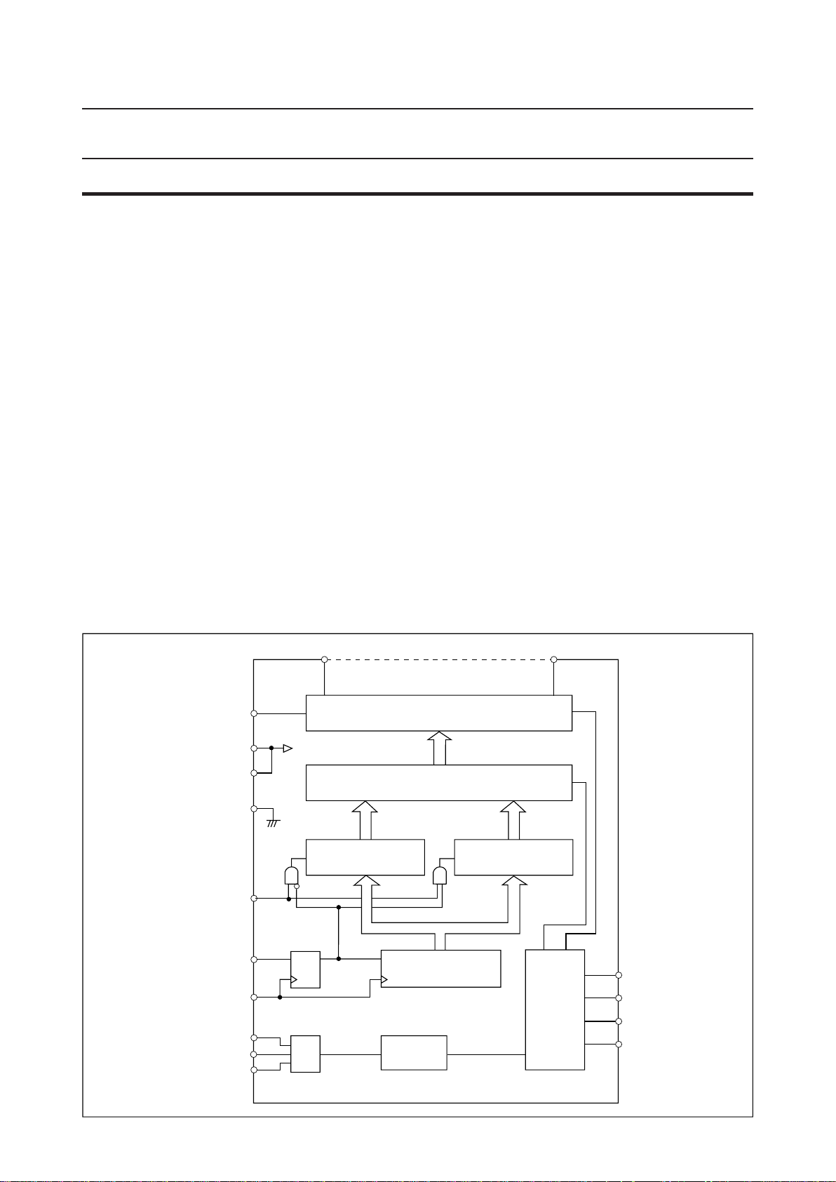
BLOCK DIAGRAM
BLANK
V
DD1
V
DD2
GND
LOAD
DATA
CLOCK
OSC-IN
OSC-C
OSC-R
SEG
1
42-DOT SEGMENT DRIVER
42-BIT SELECTOR
LL
D Q
OSC
<A>
42-BIT LATCH
42-BIT LATCH
42-BIT SI/PO
1/32
<B>
SEG
42
COMMON
DRIVER
COM-A
COM-B
V
LCM
V
LCL
1/12

PIN CONFIGURATION (TOP VIEW)
56 SEG28
55 SEG27
54 SEG26
53 SEG25
52 SEG24
51 SEG23
DD2
50 SEG22
49 V
48 SEG21
47 SEG20
46 SEG19
45 SEG1826V
44 SEG1727COM-B
43 SEG1628SEG1
MSM6544¡ Semiconductor
1SEG29
2SEG30
3SEG31
4SEG32
5SEG33
6SEG34
7SEG35
8SEG36
9SEG37
10SEG38
11SEG39
42
41
40
39
38
37
36
35
34
33
32
SEG15
SEG14
SEG13
SEG12
SEG11
SEG10
SEG9
SEG8
SEG7
SEG6
SEG5
12SEG40 31 SEG4
13SEG41 30 SEG3
14SEG42 29 SEG2
15OSC-IN
16OSC-C
17OSC-R
18LOAD
19DATA
20CLOCK
21V
22BLANK
23GND
24V
25COM-A
DD1
LCL
LCM
56-Pin Plastic QFP
2/12

MSM6544¡ Semiconductor
PIN DESCRIPTIONS
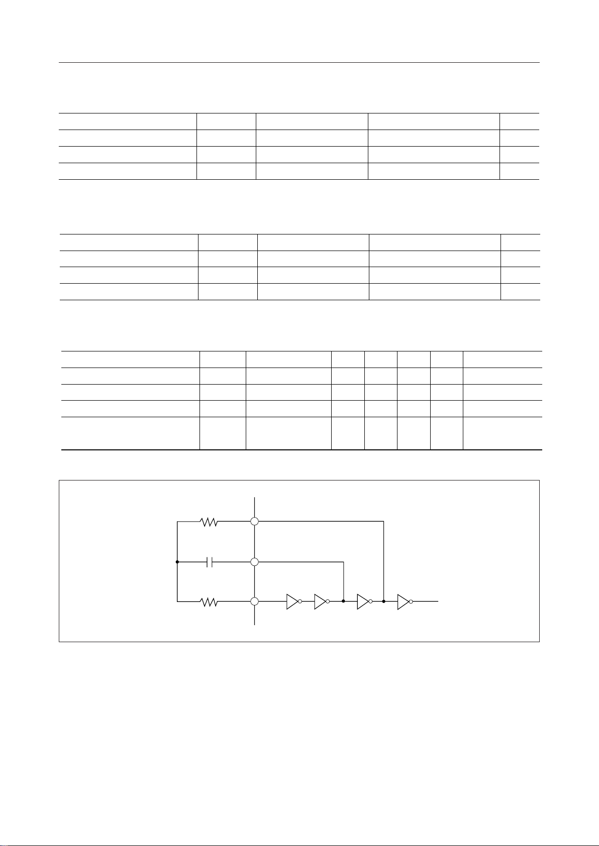
• OSC-IN, OSC-C, OSC-R
An RC oscillator circuit for 3-pin type can be configured. Since the OSC-IN pin is in a high
input impedance state, it is susceptible to noise.
• DATA-IN
This is the display data input. When this pin is at "H" level, the segments are turned on and
when at "L" level, the segments are turned off.
• CLOCK
Pin for clocking display data in. Display data is shifted on the rising edge of the clock pulse.
• LOAD
This is the signal for latching the shift register data. When this pin is set at a "H" level, the shift
register data is transmitted to LATCH <A> or LATCH <B>.
• SEG1 - SEG42
These pins drive the LCD segments.
• COM-A, COM-B
These pins drive the LCD commons. COM-A and COM-B correspond to LATCH <A> output
and LATCH <B>output, respectively.
•V
DD2
This is connected to the V
•V
LCM
pin internally.
DD1
This is the center bias pin of the LCD. Supply the middle voltage between VDD and V
•V
LCL
This is the power supply pin of the LCD driver. The contrast of the LCD can be adjusted by
changing the voltage at this pin, but do not set the voltage less than the GND level.
• BLANK
This pin is used to test the all segment outputs (SEG1 to SEG42). All segment outputs are
turned off when this pin is set to "H" level. The display returns to the condition before the pin
was set to "H" level.
•V
DD1
, GND
These are power supply voltage and ground pins.
LCL
.
3/12

ABSOLUTE MAXIMUM RATINGS
Parameter Symbol Condition Rating Unit
Supply Voltage
Input Voltage
Storage Temperature
T
V
DD
V
STG
I
T
= 25°C
a
T
= 25°C
a
—
RECOMMENDED OPERATING CONDITIONS
Parameter Symbol Condition Range Unit
Supply Voltage
Operating Temperature
LCD Driving Voltage
OSC Circuit
V
DD
T
op
V
LCD
—
—
V
DD–VLCL
–0.3 to +6.5 V
GND–0.3 to VDD +0.3
–55 to +150
3 to 6 V
–40 to +85
3 to V
DD
MSM6544¡ Semiconductor
V
°C
°C
V
Parameter Min.
Symbol Condition Typ. Max. Unit Applicable Pin
Oscillation Resistance
Oscillation Capacitance 0.001C
Current Control Resistance 33R
Common Signal Frequency 25f
R
0
C
0
R
1
0
0
1
COM
OSC-R
OSC-C
OSC-IN
— — 68 kW OSC-R
10R
Film capacitor — 0.047 mF OSC-C
— — 220 kW OSC-IN
COM-A
— — 250 Hz
COM-B
(MSM6544)
4/12
 Loading...