OKI MSM64172-xxxGS-K, MSM64172-xxxGS-2K, MSM64172-xxx Datasheet

E2E0032-38-95
¡ Semiconductor MSM64172
¡ Semiconductor
This version: Sep. 1998
Previous version: Mar. 1996
MSM64172
4-Bit Microcontroller with Built-in Serial Port and LCD Driver
GENERAL DESCRIPTION
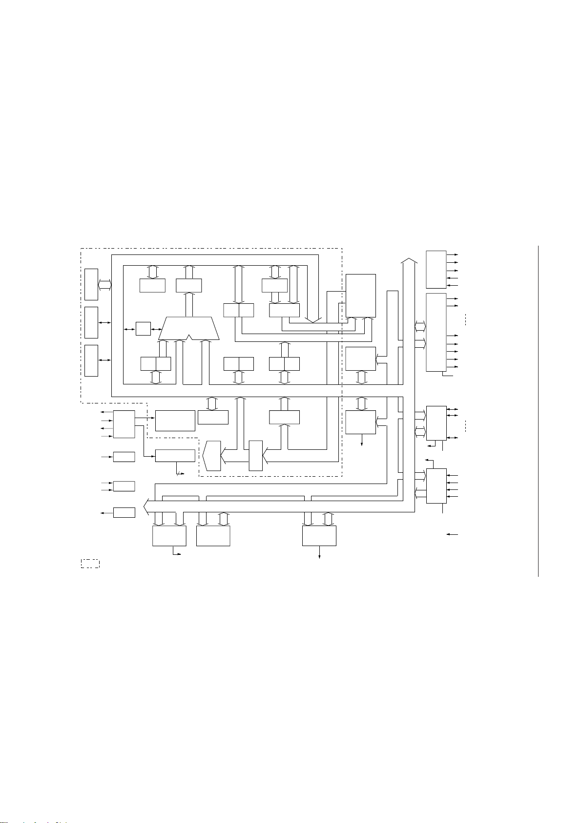
The MSM64172 is a low-power 4-bit microcontroller that incorporates Oki's original CPU core
nX-4/20. The MSM64172 has a minimum instruction execution time of 5 ms (@ 600 kHz and 3.0
V). The device includes an internal 2016-byte program memory, 128-nibble data memory, two
4-bit input-output ports, 4-bit input port, 8-bit synchronous serial port, LCD driver for up to 92
segments, and buzzer output port. Applications include low-power products with LCD
functions.
FEATURES
• Operating range
Operating frequencies
1.5 V spec. : 32.768 kHz (crystal oscillation)
3.0 V spec. low-speed clock : 32.768 kHz (crystal oscillation)
3.0 V spec. high-speed clock : 600 kHz maximum
(RC oscillation/ceramic resonator oscillation)
Operating voltage : 0.9 to 1.8 V (1.5 V spec.)
1.8 to 3.6 V (3.0 V spec.)
Operating temperature : –10 to +65°C
• Memory space
Internal program memory : 2016 bytes
Internal data memory : 128 nibbles
• Minimum instruction execution time : 5 ms @ 600 kHz (3.0 V spec. only)
91.6 ms @ 32.768 kHz
• Serial port : Clock synchro, 8-bit data transfer
• LCD driver : 27 outputs (duty ratio switchable by software)
(1) At 1/4 duty and 1/3 bias : 92 segments (max.)
(2) At 1/3 duty and 1/3 bias : 72 segments (max.)
(3) At 1/2 duty and 1/2 bias : 50 segments (max.)
• Buzzer driver : 1 output; ON/OFF controllable in four modes
• Watchdog timer
• Clock : 32.768 kHz crystal oscillator
RC oscillator/ceramic oscillator (600 kHz max.)
for high-speed clock (only for 3.0 V spec.)
CPU clock : 32.768 kHz
Switchable to high-speed clock by software
(only for 3.0 V spec.)
Time base clock : 32.768 kHz
• Power supply voltage : 1.5 V/3.0 V (selectable by mask option), low
power consumption
1/29

¡ Semiconductor MSM64172
• I/O port
Input-output port : 2 ports ¥ 4 bits
Input port : 1 port ¥ 4 bits
(16 out of the 27 LCD driver outputs can be
used as output-only ports by a mask option.)
• Interrupt sources
External interrupt : 2 sources
Internal interrupt : 5 sources
• Package options:
56-pin plastic QFP (QFP56-P-910-0.65-K) : (Product name : MSM64172-¥¥¥GS-K)
56-pin plastic QFP (QFP56-P-910-0.65-2K) : (Product name : MSM64172-¥¥¥GS-2K)
Chip : (Product name : MSM64172-¥¥¥)
¥¥¥ indicates a code number.
2/29
3/29
¡ Semiconductor MSM64172
BLOCK DIAGRAM
BSR HALT MIEF
TR2 TR0 TR1
C
ALU
BA
PCM PCL
(4)
(4)
(4)
PCH
HL XY
A11 to A8
A7 to A0
DB7 to DB0 (8)
ROM
2016B
BIAS
RAM
128N
PORT ADDRESS
IR
SIOP
INT
(8)
ROMRSP
TIMING
CONTROLLER
IR
DECODER
DB7 to DB0
PORT ADDRESS
is the CPU core (nX–4/20).
V
SS1
V
SS2
V
SS3
C1
C2
LCD
S0
S1
S22
COM1
COM0
V
SS
P1
P2
P1.0
P1.1
P2.3
INT
P0.0
P0.1
BDINTCWDT
BD
INT
TBC
INT
2CLK
RSTG
TST
VR
OSC2
OSC1
XT
XT
RESET
TST1
TST2
V
SSL
COM3/S23
COM2/S24
V
SS
INT
P0.2
V
SS
3
P0
P0.3
V
DD

¡ Semiconductor MSM64172
PIN CONFIGURATION (TOP VIEW)
)
DD
56 S11/P5.3
55 S12/P6.0
54 S13/P6.1
53 S14/P6.2
52 S15/P6.3
51 S16
50 S17
49 (V
48 S18
47 S19
46 S20
45 S2126BD
44 S2227TST1
43 COM3/S2328TST2
1S10/P5.2
2S9/P5.1
3S8/P5.0
4S7/P4.3
5S6/P4.2
6S5/P4.1
7S4/P4.0
8S3/P3.3
9S2/P3.2
10S1/P3.1
11S0/P3.0
42
41
40
39
38
37
36
35
34
33
32
COM2/S24
COM1
COM0
C2
C1
V
SS3
V
SS2
V
SS1
V
SSL
OSC1
OSC2
12P1.0 31 XT
13P1.1 30 XT
14P1.2 29 RESET
15P1.3
16P2.0
17P2.1
18P2.2
19P2.3
20VSS21VDD22P0.0
23P0.1
24P0.2
25P0.3
56-Pin Plastic QFP
Note: Pin 49 is internally connected to VDD, and VDD should be supplied from pin 21.
4/29
¡ Semiconductor MSM64172
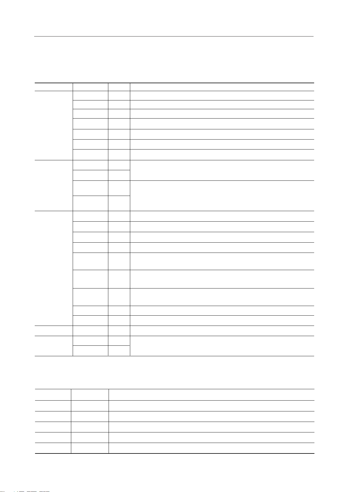
PIN DESCRIPTIONS
Basic Functions
Symbol
Power Supply
Oscillation
P0.0 to P0.3
P1.0 to P2.3
V
DD
V
SS1
V
SS2
V
SS3
V
SS
V
SSL
C1, C2
XT
XT
OSC1
OSC2
BD
TypeFunction Description
—
—
—
—
—
—
—
0 V power supply
Bias output for driving LCD (–1.5 V), or negative power supply at 1.5 V spec.
Bias output for driving LCD (–3.0 V), or negative power supply at 3.0 V spec.
Bias output for driving LCD (–4.5 V).
Negative power supply for I/O port interface
Negative power supply for internal logic (internally generated constant voltage)
Pins for connecting a capacitor for generating V
I
32.768 kHz crystal connection pins
O
High-speed clock pins :
I
A ceramic resonator and capacitors, or an external oscillation resistor (R
O
should be connected to these pins.
Input port
I
I/O
Input-output ports
Buzzer driver pin
O
SS1
, V
SS2
, and V
SS3
.
),
OS
O
LCD driver pins
O
LCD driver pins or output ports by mask option
LCD common 3 signal output pin, or segment signal output pin
O
during 1/3 or 1/2 duty
LCD common 2 signal output pin, or segment signal output pin
O
during 1/2 duty
LCD common 1 signal output pin
O
LCD common 0 signal output pin
O
Reset pin
I
I
Input pins for testing
I
Ports
Reset
Test
S16 to S22
S0/P3.0 to
S15/P6.3
COM3/S23
COM2/S24
COM1
COM0
RESET
TST1
TST2
Secondary Functions
Symbol Type Description
P1.3 I Serial data input pin (SIN)
P2.0 O
Serial data output pin (SOUT)
P2.1 O
P2.2 I/O
Serial communication ready signal output pin (SPR)
Serial communication clock input-output pin (SCLK)
P2.3 O High-speed oscillation clock monitor pin for system clock (MON)
5/29
¡ Semiconductor MSM64172
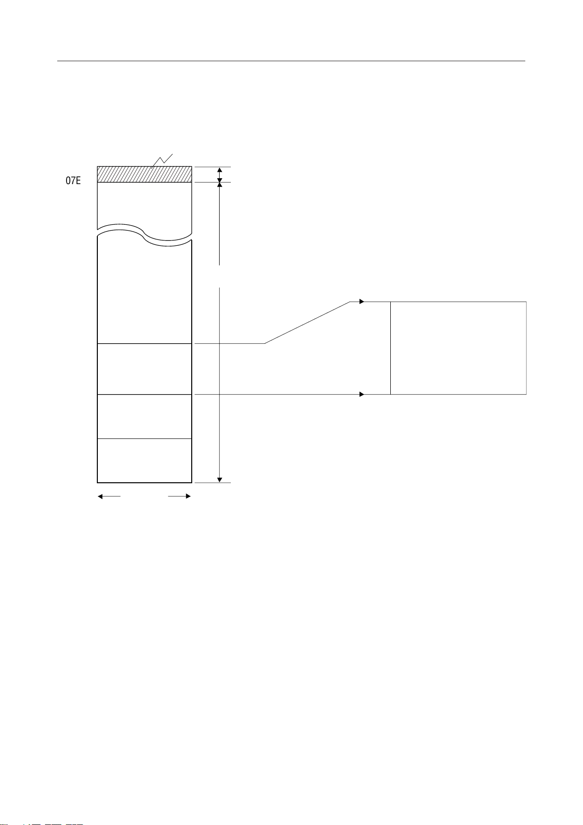
MEMORY MAPS
Program Memory
Test program area
07FFH
07E0H
03EH
020H
010H
Interrupt area
Call zero page (CZP)
area
32 bytes
2016 bytes
03BH
038H
035H
032H
029H
026H
023H
Contents of Interrupt Area
Watchdog timer interrupt
External interrupt (0)
Serial port interrupt
External interrupt (1)
32 Hz interrupt
16 Hz interrupt
1 Hz interrupt
000H
Start address
8 bits
Program Memory Map
Address 000H is the instruction execution start address after a system reset. The call zero page
(CZP) area from address 010H to address 01FH assigns the start address for the CZP subroutine
of one-byte call instruction.
The start address of an interrupt subroutine is assigned to the interrupt address from address
02DH to 03DH. The user area has 2016 bytes at addresses 000H to 07DFH. No program can be
stored in the test program area.
6/29
¡ Semiconductor MSM64172
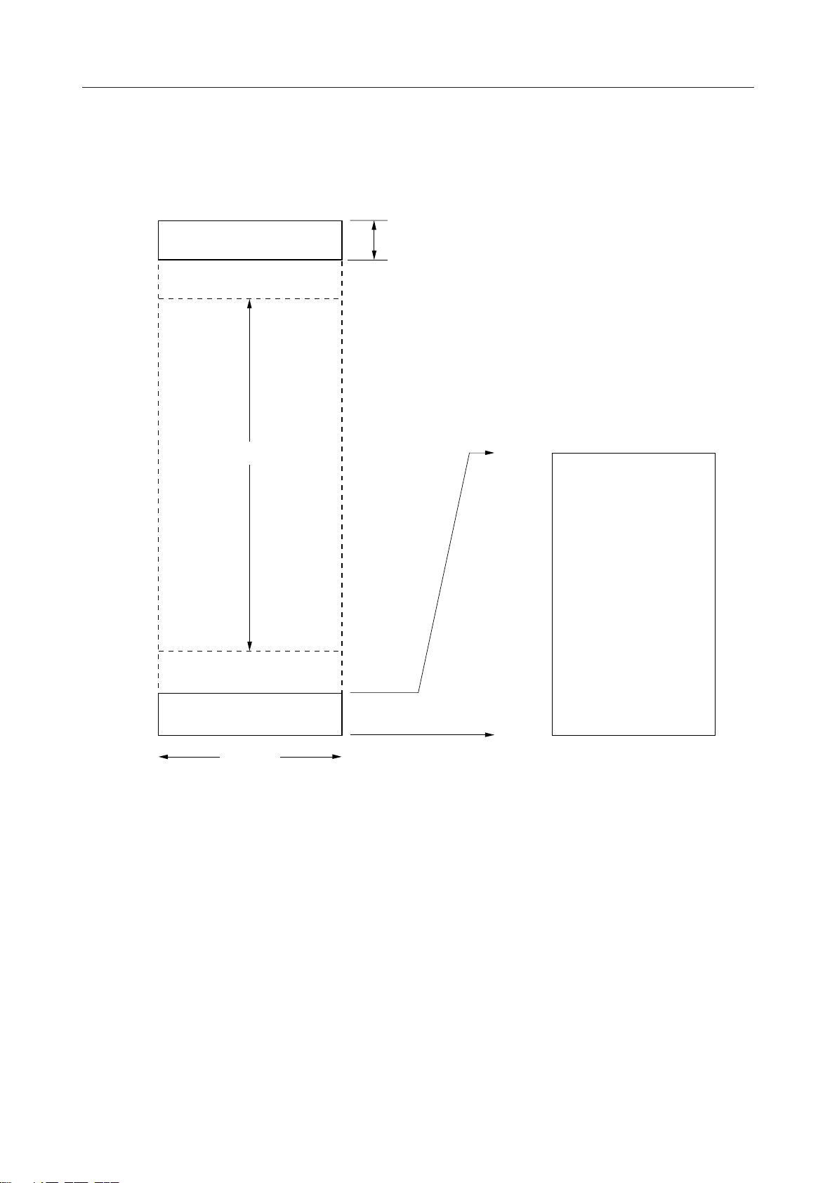
Data Memory
The data memory area consists of 8 banks and each bank has 256 nibbles (256 ¥ 4 bits).
The data RAM is assigned to BANK 7 and peripheral ports are assigned to BANK 0.
7FFH
780H
77FH
700H
BANK 7
Data RAM area
Unused area
Inaccessible area
Data/Stack area (128 nibbles)
Contents of 000H to 07FH
07FH
SFR area
0FFH
080H
07FH
000H
Unused area
BANK 0
000H
4 bits
Data Memory Map
The data RAM area (128 nibbles) is shared by the stack area. The stack is a memory starting from
address 7FFH toward the low-order addresses where 4 nibbles are used by Subroutine Call
Instruction and 8 nibbles are used by an interrupt.
The addresses 080H to 0FFH of BANK 0 and the addresses 700H to 77FH of BANK 7 are not
assigned as the data memory, so access to these addresses has no effect. Moreover, it is
impossible to access BANK 1 to BANK 6.
7/29
¡ Semiconductor MSM64172
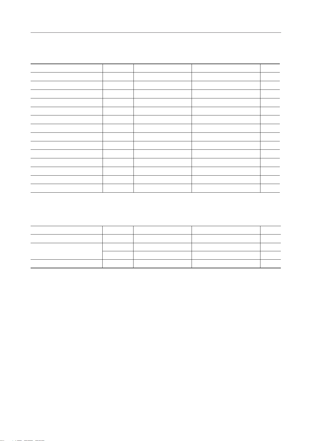
ABSOLUTE MAXIMUM RATINGS (1.5 V Spec.)
(V
= 0 V)
DD
Parameter Symbol Condition Rating Unit
Power Supply Voltage 1 V
Power Supply Voltage 2 V
Power Supply Voltage 3 V
Power Supply Voltage 4 V
Power Supply Voltage 5 V
Input Voltage 1 V
Input Voltage 2 V
Input Voltage 3 V
Output Voltage 1 V
Output Voltage 2 V
Output Voltage 3 V
Output Voltage 4 V
Output Voltage 5 V
Storage Temperature T
SS1
SS2
SS3
SSL
SS
IN1
IN2
IN3
OUT1
OUT2
OUT3
OUT4
OUT5
STG
Ta = 25°C –2.0 to +0.3 V
Ta = 25°C –4.0 to +0.3 V
Ta = 25°C –5.5 to +0.3 V
Ta = 25°C –2.0 to +0.3 V
Ta = 25°C –5.5 to +0.3 V
V
Input, Ta = 25°C V
SS1
V
Input, Ta = 25°C V
SS
V
Input, Ta = 25°C V
SSL
V
Output, Ta = 25°C V
SS1
V
Output, Ta = 25°C V
SS2
V
Output, Ta = 25°C V
SS3
V
Output, Ta = 25°C V
SS
V
Output, Ta = 25°C V
SSL
—
– 0.3 to +0.3 V
SS1
– 0.3 to +0.3 V
SS
– 0.3 to +0.3 V
SSL
– 0.3 to +0.3 V
SS1
– 0.3 to +0.3 V
SS2
– 0.3 to +0.3 V
SS3
– 0.3 to +0.3 V
SS
– 0.3 to +0.3 V
SSL
–55 to +150 °C
RECOMMENDED OPERATING CONDITIONS (1.5 V Spec.)
Parameter Symbol Condition Range Unit
Operating Temperature T
Operating Voltage
Crystal Oscillation Frequency
op
V
SS1
V
SS
f
XT
—
—
—
—
(VDD = 0 V)
–10 to +65 °C
–1.8 to –0.9 V
–5.25 to V
SS1
30 to 35 kHz
V
8/29

¡ Semiconductor MSM64172
ELECTRICAL CHARACTERISTICS (1.5 V Spec.)
DC Characteristics
(VDD = 0 V, V
= VSS = –1.5 V, Ta = –10 to +65°C unless otherwise specified)
SS1
Parameter
V
Voltage V
SS2
Voltage V
V
SS3
Voltage V
V
SSL
Symbol
Crystal Oscillation
Start Voltage
Crystal Oscillation
Hold Voltage
Crystal Oscillation
Stop Detection Time
Internal Crystal
Oscillator Capacitance
External Crystal
Oscillator Capacitance
Internal Crystal
Oscillator Capacitance
POR Generation
Voltage
POR Non-generation
Voltage
Supply Current 1 I
Supply Current 2 I
Supply Current 3 I
V
V
T
C
V
V
Condition Min. Typ. Max. Unit
+100%
SS2
Ca, Cb, C
= 0.2 mF –3.2 –3.0 –2.7 V
12
–10%
+100%
SS3
SSL
Ca, Cb, C
= 0.2 mF –4.7 –4.5 –4.1 V
12
–10%
— –1.9 –1.3 –0.6 V
Oscillation start time:
STA
within 5 seconds
HOLD
STOP
C
G
When external CG used 12 — 30 pF
GEX
C
D
When V
POR1
and –1.5 V
No POR when V
POR2
DD1
and –1.5 V
V
POR2
CPU in halt state
CPU in operating
DD2
state
— — — –0.9 V
— 0.1 — 1000 ms
— 121520pF
— 121520pF
is between V
SS1
is between
SS1
Ta = –10 to +30°C
Ta = +30 to +65°C
Ta = –10 to +30°C
Ta = +30 to +65°C
POR1
— — –0.9 V
–0.4 — 0 V
–1.5 — –1.2 V
—3 5mA
—320mA
—815mA
—825mA
Serial transfer,
f
DD3
SCK
CPU in operating
state
= 300 kHz,
Ta = –10 to +30°C
Ta = +30 to +65°C
—1025mA
—1040mA
Measuring
Circuit
1
Notes: 1. "POR" denotes Power On Reset.
2. "T
" indicates that if the crystal oscillator stops over the value of T
STOP
system reset occurs.
STOP
, the
9/29
 Loading...