

Page 1
PC2000-PC/104 Data Sheet
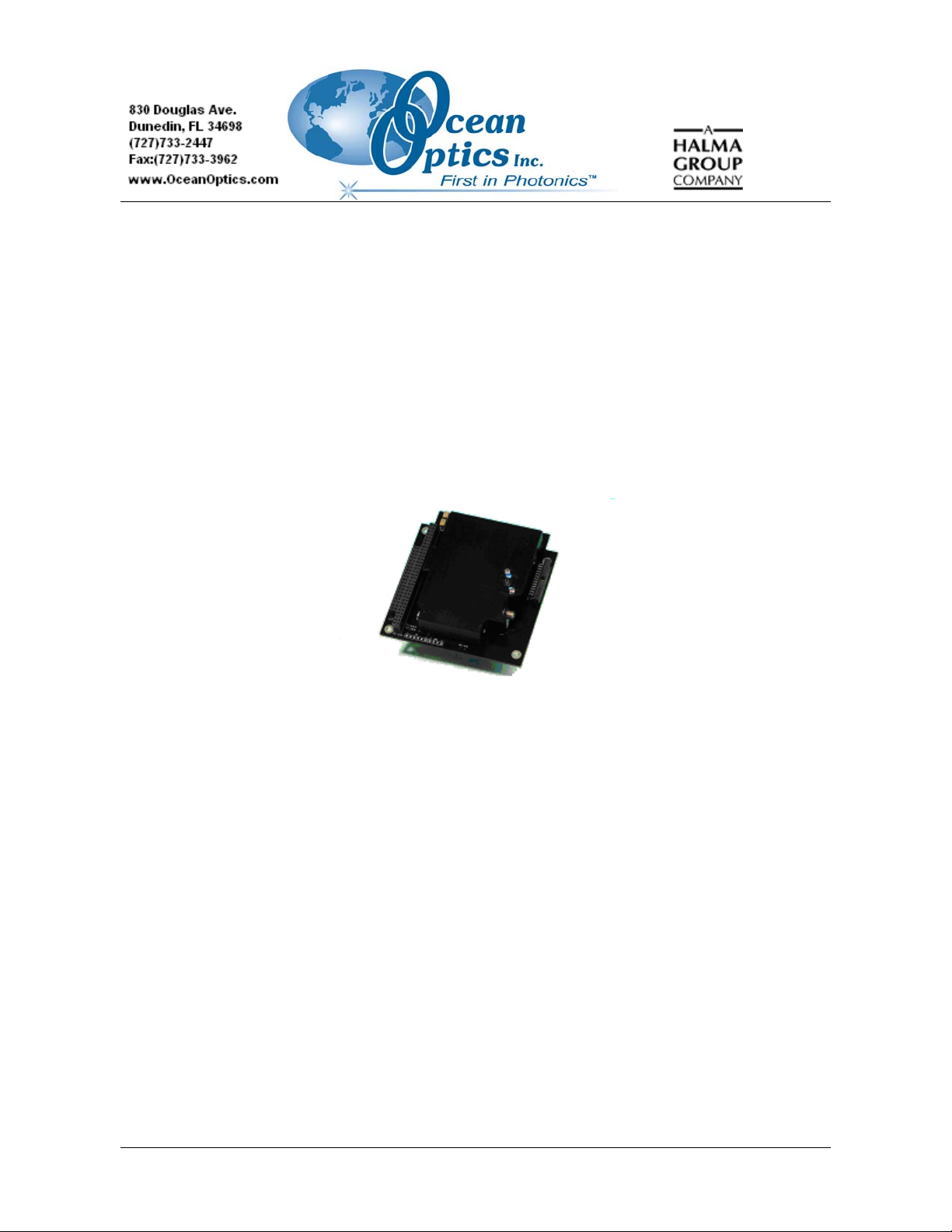
Description
The Ocean Optics OEM PC2000-PC/104 Spectrometer includes the linear CCD-array optical bench,
plus the digital interface necessary to function on a PC/104 bus. The result is a compact, flexible
system with no moving parts that's easily integrated as an OEM component.
The PC2000-PC/104 spectrometer is a unique combination of technologies providing users with both
an unusually high spectral response and good optical resolution in a single package. The electronics
have been designed for considerable flexibility in connecting to various PC2000-PC/104 series
modules as well as external interfaces. The PC2000-PC/104 can be directly coupled to as many as
seven "slave" spectrometer channels of various designs. The information included in this guide
provides detailed instructions on the connection and operation of the PC2000-PC/104.
The detector used in the PC2000-PC/104 spectrometer is a high-sensitivity 2048-element CCD array
from Sony, product number ILX511. (For complete details on this detector, visit Sony’s web site at
http://www.sel.sony.com/semi/PDF/ILX511.pdf. However, Ocean Optics applies a coating to all
ILX511 detectors, so the optical sensitivity could vary from that specified in the Sony datasheet).
000-00000-000-05-0704 1
Page 2

PC2000-PC/104 Data Sheet
Features
High sensitivity of up to 90 photons/counts
An optical resolution of 3 pixels (FWHM)
A wide variety of optics available
• 14 gratings
• 6 slit widths
• 3 detector coatings
• 6 optical filters
Integration times from 2 to >30,000 milliseconds
Modular design allows up to 7 slave spectrometer channels to operate from one master
channel
2MHz, 12 bit A/D, ± ½ bit accuracy
Supports free-running an 3 external trigger modes
Digital Interface
Memory mapped registers
Interrupt driven
2,048 deep FIFOs for on board storage
Can acquire spectra simultaneously from all 8 channels at reduced pixel density
Strobe signals for external synchronization
2 000-00000-000-05-0704
Page 3

PC2000-PC/104 Data Sheet
Specifications
Specifications Criteria
Absolute Maximum Ratings:
V
CC
Voltage on any pin
Physical Specifications:
Physical Dimensions (no enclosure)
Weight
Power:
Power requirement (master)
Supply voltage
Power-up time
Spectrometer:
Design
Focal length (input)
Focal length (output)
Input Fiber Connector
Gratings
Entrance Slit
Detector
Filters
Spectroscopic:
Integration Time
Dynamic Range
Signal-to-Noise
Readout Noise (single dark spectrum)
Resolution (FWHM)
Stray Light
Spectrometer Channels
Environmental Conditions:
Temperature
Humidity
+ 5.5 VDC
Vcc + 0.2 VDC
4.05 (W) x 3.78 (L) x 0.70 (H) inches
200 g
250 mA at +5 VDC
4.5 – 5.5 V
3 msec
Asymmetric crossed Czerny-Turner
42mm
68mm (75, 83 and 90 mm focal lengths are also available)
SMA 905
14 different gratings
5, 10, 25, 50, 100, or 200 µm slits. (Slits are optional. In the
absence of a slit, the fiber acts as the entrance slit.)
Sony ILX511 CCD
Selection of Long Pass Filters to eliminate 2
3 – >30,000 msec
8
2 x 10
250:1 single acquisition
3.5 counts RMS, 20 counts peak-to-peak
0.03 – 10.0 nm varies by configuration
<0.05% at 600 nm; <0.10% at 435 nm
8 (master plus 7 slaves)
-30° to +70° C Storage & -10° to +60° C Operation
0% - 90% noncondensing
nd
order (optional)
000-00000-000-05-0704 3
Page 4

PC2000-PC/104 Data Sheet
Electrical Pinouts
J2 Electrical Connector
Pin I/O Function Pin I/O Function
1 I Analog Channel 1 14 Gnd
2 I Analog Channel 2 15 N/C Reserved – D2
3 I Analog Channel 3 16 N/C Reserved – D0
4 I Analog Channel 4 17 O Continuous Strobe
5 I Analog Channel 5 18 I External Hardware Trigger
6 I Analog Channel 6 19 O Array Clock Output
7 I Analog Channel 7 20 O Lamp Enable - S0
8 Vcc 21 O Single Strobe
9 O CCD Temperature 22 I External Sync Input
10 Vcc 23 O Read Out Gate
11 Gnd 24 N/C Reserved – D1
12 N/C 25 N/C Reserved – D3
13 Gnd 26 I Software Trigger
J2 on PC104 is Samtec #STMM-113-02-S-D-RA, the mating part is a ribbon cable #TCSD-13-D(length)-01--other mating options are SQT,SQW,ESQT,TLE,SMM,MMS
Pin Function Description
Function Description
Analog Channel 0 - 7
V
CC
GND The ground (supply voltage return) or case ground.
Lamp Enable Software-controlled TTL signal commonly used for activation of Light Sources
Software Trigger
Single Strobe
Continuous Strobe
External Hardware Trigger
External Sync Input Trigger
CCD Temperature
The analog signals that correspond to the output from the 8 spectrometer
channels. Inputs for channels 1-7 are available on J1.
The positive supply voltage +5VDC.
Active high TTL input signal used to trigger the acquisition system in the
External Software Trigger mode.
TTL output signal used to pulse a strobe that is high at the start of each
integration period.
TTL output signal used to pulse a strobe that is divided down from the Master
Clock signal.
TTL trigger signal (rising edge trigger input) used in External Hardware Trigger
mode.
TTL signal used to define the integration time (time between rising edges)
when using the External Synchronization Trigger mode.
Analog signal generated from an LM35 mounted in close proximity to the
CCD. The analog output is 10mv/C.
4 000-00000-000-05-0704
Page 5

PC2000-PC/104 Data Sheet
Interface Information
Pixel Definition
A series of pixels in the beginning of the scan have been covered with an opaque material to
compensate for thermal induced drift of the baseline signal. As the PC2000-PC/104 warms up, the
baseline signal will shift slowly downward a few counts depending on the external environment.
(Temperature-regulated units do not exhibit this shift.) The baseline signal is set between 50 and 100
counts at the time of manufacture. If the baseline signal is manually adjusted, it should be left high
enough to allow for system drift. The following is a description of all of the pixels:
Pixel Description
0–1 Not usable
2–24 Optical black pixels
24–25 Transition pixels
26–2674 Optical active pixels
It is important to note that Ocean Optics A/D products only digitize the first 2048 pixels, as they all
have a 2048 x 16 FIFO buffer.
Analog Section
The PC2000-PC/104 is capable of supporting the output of up to 8 spectrometer channels (master
channel plus 7 slave channels). The spectrometer channel is determined by switch SW2. Within a
stack, there should be only one spectrometer on any given channel. The master spectrometer is
hardwired to the master channel (channel 0). Each spectrometer generates an analog signal (-2.5 +2.5V), which corresponds to the input spectra.
Clock Signals
Master Clock
The frequency of this clock is set via software. The A/D rate is one-half that of the Master Clock. The
maximum rate for the Master Clock is 4MHz, which equates to an A/D rate of 2 MHz. A
recommended minimum frequency is 100 kHz.
Integration Clock
The frequency of this clock is set via software. The period for the integration time clock should be
longer than 4100 master clock periods in order to read the entire array. This equates to 1.1ms.
000-00000-000-05-0704 5
Page 6

PC2000-PC/104 Data Sheet
Strobe Signals
Single Strobe
The Single Strobe signal is a TTL HIGH pulse that occurs at the start of each integration period. This
pulse occurs 2 master clock cycles after the start of the integration period. The pulse is not generated
unless The Lamp Enable (S0) signal is set (Digital 1-TTL HIGH) in software.
Continuous Strobe
The Continuous Strobe signal is a pulse-train (50% duty cycle) whose frequency is determined by
software.
Synchronizing Strobe Events
For some applications it is necessary to view pulsed sources. If the application requires more than one
pulse per integration period, exercise care to insure a stable signal. The integration time must be set so
that an equal number of strobe events occurs during any given integration period. This synchronization
only occurs when the integration period is a multiple of a power of 2, since the strobe signal is the
master clock divided by a power of 2.
Triggering Modes
The PC2000-PC/104 supports four triggering modes, which are defined by the state of the software
controlled S0 and S1. Details of each triggering mode are discussed below.
Mode S1 S0
Normal 0 X
Software Trigger 0 X
Ext Synchronization 1 0
Ext Hardware Trigger 1 1
Normal (S1:S0 = 0:X)
In this mode, the PC2000-PC/104 uses the user-supplied integration clock (DB25: pin 23) and
continuously scans the CCD array.
External Software Trigger (S1:S0 = 0:X)
In this mode, the PC2000-PC/104 uses the normal integration clock. Since this mode is under software
control its functionality can be software defined. In this mode, Ocean Optics software, waits until the
Software Trigger Input (D3) line goes HIGH before it acquires an acquisition. The amount of delay
between the trigger pulse and when a spectrum is acquired is indeterminate because the delay is
dependent upon (1) how fast the software polls the D3 line and recognizes it is HIGH and (2) the
amount of time until the start of the next integration period. The integration time is under user control
in this mode. This mode must be implemented in the software that controls the data acquisition.
6 000-00000-000-05-0704
Page 7

PC2000-PC/104 Data Sheet
External Synchronization (S1:S0 = 1:0)
In this mode, the effective integration time is the time between rising edges of the signal applied to the
External Synchronization pin (J2:Pin 22). This mode is useful for synchronizing the integration time to
an external clock source.
External Hardware Trigger (S1:S0 = 1:1)
In this mode, the PC2000-PC/104 uses an internally generated integration clock that is triggered by the
rising edge of the External Hardware Trigger signal (J2:pin 18). On the rising edge of this signal, the
internal logic resets the CCD array, integrates for 2.1ms and then clocks out the array.
CCD Detector Temperature
Also available is an optional temperature sensor, which when included is located directly under the
detector. The output of this signal is fed to H2: pin 6. The typical error of the sensor is
o
25
C. The output is calibrated directly in oC with a scale factor of 10 mV/oC.
o
±
C around
Software Interface
Overview
The PC2000-PC104 employ a memory mapped set of registers, which control all of the functionality.
The register definition is shown in
Communications with the spectrometer are through a base address, which is defined by switch
settings.
Performing an 8-bit read from this port will provide the state of the Software Trigger input on the D3
line (i.e., Read Value & 0x04 to determine Trigger Input line state).
Software Trigger Port (base + 5) Bit Description
Read Spectral Data (base + 6) Bit Description
Performing a 16-bit read from this port will return one spectral data point. To obtain full spectra
perform 2048 reads after interrupt initiation. Raw data format is signed—invert bit 11 to convert to
unsigned (i.e. Data Value XOR’ed with 0x0800).
Table 1. PC2000-PC104 Programming Registers.
Channel Rotation Port (base + 7) Bit Description
Byte wide writes to this port activates or deactivates the rotator. If activated, the value written
determines the number of channels rotated through.
000-00000-000-05-0704 7
Page 8

PC2000-PC/104 Data Sheet
Value Written Function
0 Disables channel rotation
9 (0x09) Rotates channels 0 and 1
10 (0x0A) Rotates channels 0 through 2
11 (0x0B) Rotates channels 0 through 3
12 (0x0C) Rotates channels 0 through 4
13 (0x0D) Rotates channels 0 through 5
14 (0x0E) Rotates channels 0 through 6
15 (0x0F) Rotates channels 0 through 7
Table 2. Switch Settings for Base Address and IRQ illustrates how to configure the switch settings for
the desired base address. Once a spectra is acquired and ready to be readout, the spectrometer
generates an IRQ. The specific IRQ is defined by switch setting as listed in
Settings
.
Table 1. PC2000-PC104 Programming Registers
Port Address PC2000-PC104 Register Description
IRQ Interrupt Request
base + 0 Master Clock Counter Port (base frequency is 8 MHz)
base + 1 Continuous Strobe Counter Port (base frequency is 976 Hz)
base + 2 Integration Clock Counter port (base frequency is 976 Hz)
base + 3 N/A
base + 4 Command port (output only)
base + 5 Software Trigger Digital Input port (bit 3 only)
base + 6 Read Spectral Data (WORD Access)
base + 7 Channel rotation command port
Counter Ports (Base – Base +2) Description
Output frequency of counter is base frequency divided by the 16bit value written to this port. Limits
for the various counters along with the corresponding counter value are provided below.
Counter Min Typical Max
Master Clock 4Mhz 2 4Mhz 2
Continuous Strobe
2.048ms period
2
Integration Clock
8 000-00000-000-05-0704
3.072ms period
3
Page 9

PC2000-PC/104 Data Sheet
Command Port (Base +4) Bit Description
Writes to this 8-bit port control the spectrometer’s functionality.
Bit Function
7 MUX address bit 2
6 Enable board interrupt (1=enabled)
5 Master reset to clear FIFO (1=reset)
4 MUX address bit 1
3 MUX address bit 0
2 Spectrometer mode control S1
1
0 Read enable (1=enabled)
Spectrometer mode control S0
Multiplexed as Strobe enable (1=enabled)
Software Trigger Port (base + 5) Bit Description
Performing an 8-bit read from this port will provide the state of the Software Trigger input on the D3
line (i.e., Read Value & 0x04 to determine Trigger Input line state).
Read Spectral Data (base + 6) Bit Description
Performing a 16-bit read from this port will return one spectral data point. To obtain full spectra
perform 2048 reads after interrupt initiation. Raw data format is signed—invert bit 11 to convert to
unsigned (i.e. Data Value XOR’ed with 0x0800).
Channel Rotation Port (base + 7) Bit Description
Byte wide writes to this port activates or deactivates the rotator. If activated, the value written
determines the number of channels rotated through.
000-00000-000-05-0704 9
Page 10

PC2000-PC/104 Data Sheet
Value Written Function
0 Disables channel rotation
9 (0x09) Rotates channels 0 and 1
10 (0x0A) Rotates channels 0 through 2
11 (0x0B) Rotates channels 0 through 3
12 (0x0C) Rotates channels 0 through 4
13 (0x0D) Rotates channels 0 through 5
14 (0x0E) Rotates channels 0 through 6
15 (0x0F) Rotates channels 0 through 7
Table 2. Switch Settings for Base Address and IRQ
Base Address Settings
Switches 1 – 6 of SW1 determine the base address, which is the weighted sum of these switches. The switch
position is negative logic (i.e. 1 is off). The factory default is 0x300 hex or 768 decimal.
Switch # Address line Value (hex) Value (decimal) Switch setting for 300
Switch position
hex
1 A4 10h 16 on 0
2 A5 20h 32 on 0
3 A6 40h 64 on 0
4 A7 80h 128 on 0
5 A8 100h 256 off 1
6 A9 200h 512 off 1
IRQ Interrupt Request Settings
The following matrix defines the different Interrupt Request settings by switch positions 7, 8, and 9. In
the default setting, the IRQ is set to 7. Combinations for IRQ settings follow.
Switch Settings
#7 #8 IRQ
0 0 3
1 0 4
0 1 5
1 1 7 (Default)
1 indicates a switch in the ON position
10 000-00000-000-05-0704
Page 11

PC2000-PC/104 Data Sheet
Counters
The PC2000-PC104 implemented the core of an 82C54 programmable timer in the FPGA to
implement the required clock signals. Refer to this data sheet for more detailed information. This
implementation requires no control word to be written to the counter. These timers use the equivalent
of control mode 3 (50% duty cycle) and the counters are always enabled. The base frequency for each
of the timers is shown in Table 1.
Programming
Pseudo-code programming for the PC2000-PC104 is provided in PC2000-PC/104 Programming
Sequence
.
PC2000-PC/104 Programming Sequence
This technical document describes the programming procedures necessary to control and PC2000PC104 spectrometer. This setup is functionally identical to the S2000 spectrometer and ADC1000 ISA
card. The pseudo-code examples below use the following definitions:
(Note: all numbers starting with "0x" are in hexidecimal.)
• source code is in this font
comments are in this font
• outport_byte(baseadd+1,0x13) -- outputs one byte of data to the specified port,
represented as an offset from the base address
• outport_word(baseadd+1,0xffff) -- outputs one word of data to the specified port,
represented as an offset from the base address
• inport_byte(baseadd+3) -- inputs one byte of data from the specified port,
represented as an offset from the base address
• inport_word(baseadd+5) -- inputs two bytes (one 16-bit word) of data from the
specified port, represented as an offset from the base address
• Variables:
baseadd -- the base address in decimal, 16-bit integer
dsf -- digital sample frequency, or A/D conversion frequency, 16-bit integer
fdc -- number of flashes per scan, 16-bit integer
cmd -- command to be sent to A/D card, 8-bit (unsigned) integer
average -- number of scans to average
oldvect -- stored interrupt vector
current_channel -- active spectrometer channel
indata -- data read from the A/D card
irq -- the interrupt number (interrupt request) of the ADC500/ADC1000/PC1000
ihandler -- the interrupt handler function
000-00000-000-05-0704 11
Page 12

PC2000-PC/104 Data Sheet
• Operators:
>> bit shift operator
== equal comparison operator
& bit-wise AND operator
^ bit-wise XOR operator
| bit-wise OR operator
One internal pseudo-code function is used --
CheckTriggerMode(). This function checks the trigger
mode and sets the appropriate spectrometer mode control bits (S0 and S1) in the command sent to the
ADC500/ADC1000 control port. The psuedo-code for this function is:
if trigger_mode = external_synchronization then cmd = cmd | 0x04
if trigger_mode = external_hardware_trigger then cmd = cmd | 0x06
if trigger_mode = software_trigger then cmd = cmd & 0xf9
if trigger_mode = no_trigger then cmd = cmd & 0xf9
Step 1: Initialize A/D Functions
outport_word(baseadd+1,0x0010)
outport_word(baseadd,0x0002)
cmd = 0x20
CheckTriggerMode()
outport_byte(baseadd+4,cmd)
delay(10)
cmd = 0x00
CheckTriggerMode()
outport_byte(baseadd+4,cmd)
Loads counter 1, which is set to a ~10 msec period.
Loads counter 0, which is set to 4Mhz
master reset
check the external trigger mode
send command to ADC500/ADC1000
delay for 10 msec to allow "settling"
cancel reset and leave disabled
check the external trigger mode
send command to ADC500/ADC1000
This function initializes the A/D card. First, the countinuous strobe counter (1) is loaded with a divisor
so that the resulting period is ~10 msec. Next the Master Clock counter is initialized to the fasted
possible value (4MHz). The A/D card is reset and disabled.
Step 2: Setup Integration Time
if dsf < 3 then dsf = 3
outport_word(baseadd+2,
dsf)
if dsf < 25 then delay(25)
else delay(12*dsf/10)
This function sets the integration time of the spectrometer. There must be a delay after this setting to
allow the previous integration period to complete before the new one begins.
make sure integration time is not below the allowable minimum
load counter 2, which defines the integration time
delay to allow the previous cycle to complete before we start the next
integration cycle
12 000-00000-000-05-0704
Page 13

PC2000-PC/104 Data Sheet
Step 3: Install Your Interrupt Vector
Consult your hardware documentation to determine how to do this correctly. Below is a sample C
function, which installs the interrupt service routine using Borland C 4.0 in a DOS environment.
disable()
oldvect = getvect(irq + 8)
setvect(irq + 8, ihandler)
if irq == 2 then outport_byte(0x21,
inport_byte(0x21) & 0xfb)
if irq == 3 then outport_byte(0x21,
inport_byte(0x21) & 0xf7)
if irq == 5 then outport_byte(0x21,
inport_byte(0x21) & 0xdf)
if irq == 7 then outport_byte(0x21,
inport_byte(0x21) & 0x7f)
enable()
disable interrupts during this change
save the old interrupt vector for the IRQ
set the interrupt vector to be the address of your
interrupt handler
unmask the correct IRQ
unmask the correct IRQ
unmask the correct IRQ
unmask the correct IRQ
reenable interrupts once done changing
After disabling interrupts, we store the old interrupt vector for the IRQ in oldvect. We then set the new
interrupt vector to a function called ihandler (described below). Then, we enable a specific interrupt by
changing the interrupt mask.
Step 4: Trigger a Data Acquisition Cycle
port = baseadd + 4
cmd = cmd & 0xe7
if current_channel between Master
and Slave3 then
cmd = cmd | current_channel << 3
cmd = cmd & 0x7f
else
cmd = cmd | current_channel << 3
cmd = cmd | 0x80
end if
identify the PC2000-PC104 control port
clear the channel bits
set the A/D MUX channel. If the MUX channel is
between 0 and 3, the highest order bit for the MUX
selection is set to 0, or else it is set to 1.
CheckTriggerMode()
outport_byte(port,cmd)
cmd = cmd & 0xbe
cmd = cmd | 0x20
CheckTriggerMode()
outport_byte(port,cmd)
cmd = cmd & 0xdf
CheckTriggerMode()
000-00000-000-05-0704 13
check the external trigger mode
set command to PC2000-PC104
disable triggers and interrupts
reset the FIFO buffer
check the external trigger mode
set command to PC2000-PC104
cancel the reset
check the external trigger mode
Page 14

PC2000-PC/104 Data Sheet
outport_byte(port,cmd)
cmd = cmd | 0x41
if external software triggering then
while inport_byte(baseadd + 5) & 8)
== 0 wait on this line
CheckTriggerMode()
if not scanning a dark spectrum or
using external triggering then
cmd = cmd | 2
outport_byte(port,cmd)
set command to PC2000-PC104
enable interrupts and triggers
if you are external triggering, constantly query the
digital input on pin 26 of the 26 pin connector to check
for it to go high (+5VDC)
check the external trigger mode
if you are scanning a dark spectrum or using an external
trigger mode do not turn on the flash
set command to PC2000-PC104
This function does a lot. First, it identifies the PC2000-PC104 control port as baseadd + 4. It then
clears the MUX address of the A/D, sets the MUX address of the A/D, turns off the flash-during-scan,
resets the FIFO buffer, cancels the FIFO reset, enables the triggers and interrupt (
IMPORTANT, as it is
what makes it all work), and waits for an external software trigger on pin 8
this is VERY
of the DSUB15 connector, if requested. The function then triggers a scan.
Step 5: Service the Interrupt
When a scan is completed, your program is notified by an interrupt. You MUST service this interrupt
IMMEDIATELY. The interrupt service routine (ISR) must be as short as possible. Do as little
processing as possible in the ISR. The following is our ISR.
cmd = cmd & 0xbe
CheckTriggerMode()
outport_byte(baseadd + 4,cmd)
enable()
for i = 0 to 2047
indata(i) = (inport_word(baseadd + 6)
^ 0x0800) & 0x0fff
next i
cmd = cmd & 0xbe
cmd = cmd | 0x20
CheckTriggerMode()
outport_byte(baseadd + 4,cmd)
cmd = cmd & 0xdf
CheckTriggerMode()
outport_byte(baseadd + 4,cmd)
outport_byte(0x20,0x20)
turn interrupts and triggers off
check the external trigger mode
stop the acquisition
restart interrupts
read 2048 data points from the FIFO buffer, convert to
unsigned values and mask off upper 4 bits (0-4095
value)
turn interrupts and triggers off
reset the A/D cards FIFO
check the external trigger mode
issue the command
cancel the reset
check the external trigger mode
issue the command
send a non-specific EOI (end of interrupt) to the 8259
interrupt controller chip
14 000-00000-000-05-0704
Page 15

PC2000-PC/104 Data Sheet
Many actions happen at interrupt time. First, we disable the PC2000-PC104 so that it does not
continue to scan. Then, we read the data from the FIFO. After the data is read, the spectrometer is
reset. You must be sure to tell the computer you have serviced the interrupt. That is done by issuing a
non-specific end-of-interrupt (EOI) to the 8259 interrupt controller chip by outport_byte(0x20,0x20).
At the end of this function, if you wish to immediately capture another scan, you can call the function
in
Step 4: Trigger a Data Acquisition Cycle after the outport_byte(0x20,0x20) function call.
Step 6: Remove the Interrupt Handler
When you are done with the driver communicating with the spectrometer, you must return the
interrupt vector to its original state. Again, this function will depend on your operating environment,
and we provide a sample in Borland C 4.0 for DOS.
Disable()
if irq == 2 then outport_byte(0x21,
inport_byte(0x21) | 0x04)
if irq == 3 then outport_byte(0x21,
inport_byte(0x21) | 0x08)
if irq == 5 then outport_byte(0x21,
inport_byte(0x21) | 0x20)
if irq == 7 then outport_byte(0x21,
inport_byte(0x21) | 0x21)
Setvect(irq + 8,oldvect)
enable()
disable interrupts during this change
mask the correct IRQ
mask the correct IRQ
mask the correct IRQ
mask the correct IRQ
restore the old interrupt vector
reenable interrupts once the change is
completed
000-00000-000-05-0704 15
Page 16

PC2000-PC/104 Data Sheet
16 000-00000-000-05-0704
 Loading...