

Page 1

TEA5767HN
Low-power FM stereo radio for handheld applications
Rev. 05 — 26 January 2007 Product data sheet
1. General description
The TEA5767HN is a single-chip electronically tuned FM stereo radio for low-voltage
applications with fully integrated Intermediate Frequency (IF) selectivity and
demodulation. The radio is completely adjustment-free and only requires a minimum of
small and low cost external components. The radio can be tuned to the European, US,
and Japanese FM bands.
2. Features
n High sensitivity due to integrated low-noise RF input amplifier
n FM mixer forconversion to IF of the US/Europe (87.5 MHz to 108 MHz) and Japanese
(76 MHz to 91 MHz) FM band
n Preset tuning to receive Japanese TV audio up to 108 MHz
n RF Automatic Gain Control (AGC) circuit
n LC tuner oscillator operating with low cost fixed chip inductors
n FM IF selectivity performed internally
n No external discriminator needed due to fully integrated FM demodulator
n Crystal reference frequency oscillator; the oscillator operates with a 32.768 kHz clock
crystal or with a 13 MHz crystal and with an externally applied 6.5 MHz reference
frequency
n Phase-locked loop (PLL) synthesizer tuning system
n I2C-bus and 3-wire bus, selectable via pin BUSMODE
n 7-bit IF counter output via the bus
n 4-bit level information output via the bus
n Soft mute
n Signal dependent mono to stereo blend [Stereo Noise Cancelling (SNC)]
n Signal dependent High Cut Control (HCC)
n Soft mute, SNC and HCC can be switched off via the bus
n Adjustment-free stereo decoder
n Autonomous search tuning function
n Standby mode
n Two software programmable ports
n Bus enable line to switch the bus input and output lines into 3-state mode
Page 2

NXP Semiconductors
3. Quick reference data
Table 1. Quick reference data
V
CCA=VCCD=VCC(VCO)
for V
the emf value is given; unless otherwise specified.
RF
Symbol Parameter Conditions Min Typ Max Unit
V
CCA
V
CC(VCO)
V
CCD
I
CCA
I
CC(VCO)
I
CCD
f
FM(ant)
T
amb
FM overall system parameters; see
V
RF
S
−200
S
+200
V
AFL
V
AFR
analog supply voltage
Voltage-Controlled
Oscillator (VCO)
supply voltage
digital supply voltage
analog supply current operating; V
VCO supply current operating; V
digital supply current operating; V
FM input frequency 76 - 108 MHz
ambient temperature V
RF sensitivity input
voltage
low side 200 kHz
selectivity
high side 200 kHz
selectivity
left audio frequency
output voltage
right audio frequency
output voltage
= 2.7 V; T
TEA5767HN
Low-power FM stereo radio for handheld applications
=25°C; AC values are given in RMS;
amb
[1]
2.5 3.0 5.0 V
[1]
2.5 3.0 5.0 V
[1]
2.5 3.0 5.0 V
= 3 V 6.0 8.4 10.5 mA
CCA
Standby mode; V
CC(VCO)
Standby mode; V
CCD
Standby mode; V
bus enable line HIGH 30 56 80 µA
bus enable line LOW 11 19 26 µA
CCA=VCC(VCO)=VCCD
2.5 V to 5 V
Figure 13
fRF= 76 MHz to 108 MHz;
∆f = 22.5 kHz; f
(S+N)/N = 26 dB;
de-emphasis = 75 µs; L = R;
B
= 300 Hz to 15 kHz
AF
∆f=−200 kHz;
f
= 76 MHz to 108 MHz
tune
∆f = +200 kHz;
f
= 76 MHz to 108 MHz
tune
VRF=1mV; L=R;
∆f = 22.5 kHz; f
de-emphasis = 75 µs
VRF=1mV; L=R;
∆f = 22.5 kHz; f
de-emphasis = 75 µs
=3V - 3 6 µA
CCA
= 3 V 560 750 940 µA
CC(VCO)
=3V - 1 2 µA
= 3 V 2.1 3.0 3.9 mA
=3V
CCD
=
−10 - +75 °C
- 2 3.5 µV
= 1 kHz;
mod
[2]
32 36 - dB
[2]
39 43 - dB
60 75 90 mV
= 1 kHz;
mod
60 75 90 mV
= 1 kHz;
mod
TEA5767HN_5 © NXP B.V. 2007. All rights reserved.
Product data sheet Rev. 05 — 26 January 2007 2 of 40
Page 3

NXP Semiconductors
TEA5767HN
Low-power FM stereo radio for handheld applications
Table 1. Quick reference data
V
CCA=VCCD=VCC(VCO)
for V
the emf value is given; unless otherwise specified.
RF
Symbol Parameter Conditions Min Typ Max Unit
(S+N)/N maximum signal plus
noise-to-noise ratio
α
cs(stereo)
stereo channel
separation
THD total harmonic
distortion
[1] V
[2] Low side and high side selectivity can be switched by changing the mixer from high side to low side LO
, V
CCA
injection.
CC(VCO)
4. Ordering information
Table 2. Ordering information
Type number Package
TEA5767HN HVQFN40 plastic thermal enhanced very thin quad flat package;
…continued
= 2.7 V; T
=25°C; AC values are given in RMS;
amb
VRF=1mV; L=R;
∆f = 22.5 kHz; f
mod
= 1 kHz;
54 60 - dB
de-emphasis = 75 µs;
B
= 300 Hz to 15 kHz
AF
VRF= 1 mV; R = L = 0 or R = 0
24 30 - dB
and L = 1 including 9 % pilot;
∆f = 75 kHz; f
mod
= 1 kHz;
data byte 3 bit 3 = 0;
data byte 4 bit 1 = 1
V
=1mV; L=R;
RF
∆f = 75 kHz; f
mod
= 1 kHz;
- 0.4 1 %
de-emphasis = 75 µs
and V
must not differ by more than 200 mV.
CCD
Name Description Version
SOT618-1
no leads; 40 terminals; body 6 × 6 × 0.85 mm
TEA5767HN_5 © NXP B.V. 2007. All rights reserved.
Product data sheet Rev. 05 — 26 January 2007 3 of 40
Page 4
TEA5767HN_5 © NXP B.V. 2007. All rights reserved.
Product data sheet Rev. 05 — 26 January 2007 4 of 40
xxxx xxxxxxxxxxxxxxxxxxxxxxxxxxxxxx x xxxxxxxxxxxxxx xxxxxxxxxx xxx xxxxxx xxxxxxxxxxxxxxxxxxxxxxx xxxxxxxxxxxxxxxxxxxxxx
xxxxx xxxxxx xx xxxxxxxxxxxxxxxxxxxxxxxxxxxxx xxxxxxxxxxxxxxxxxxxxxx xxxxxxxxxxx xxxxxxx xxxxxxxxxxxxxxxxxxx
xxxxxxxxxxxxxxxx xxxxxxxxxxxxxx xxxxxx xx xxxxxxxxxxxxxxxxxxxxxxxxxxxxxxxx xxxxxxxxxxxxxxxxxxxxxxxx xxxxxxx
xxxxxxxxxxxxxxxxxxxxxxxxxxxxxxxxxxxxxxxxxxxxxx xxxxxxxxxxx xxxxx x x
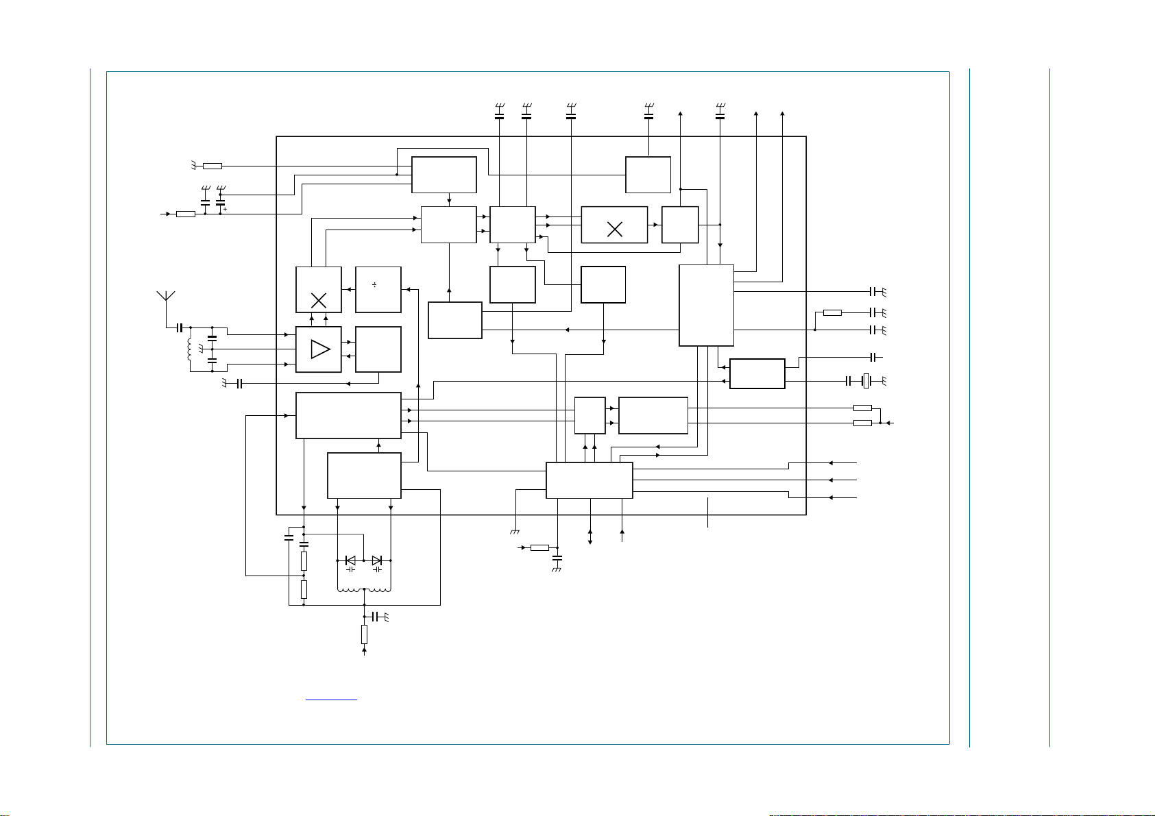
5. Block diagram
NXP Semiconductors
V
CCA
FM antenna
22 nF
4.7 Ω
100 pF
L1
47 nF 47 nF 33 nF
LIMDEC2
29 28 27 26 25
R1
22 µF
27 pF
47 pF
4.7 nF
I
gain
AGND
V
CCA
RFI1
RFGND
RFI2
TAGC
LOOPSW
32
33
34
I/Q-MIXER
1st FM
35
36
37
38
39
TUNING SYSTEM
23
CPOUT VCOTANK2 V
39 nF10 nF
10 kΩ
100 kΩ
AGC
VCO
VCOTANK1
D1L3D2
2
N1
L2
GAIN
STABILIZATION
RESONANCE
AMPLIFIER
IF CENTRE
FREQUENCY
ADJUST
programmable divider output
reference frequency divider output
45
CC(VCO)
LIMDEC1 TIFC V
LIMITER
LEVEL
ADC
6789
DGND CLOCK
12 Ω
V
CCD
47 nF
DEMODULATOR
COUNTER
I
ref
MUX
I2C-BUS
AND
3-WIRE BUS
CCD
22 nF
IF
TEA5767HN
PROGRAMMABLE
DATAV
ref
POWER
SUPPLY
SOFTWARE
PORT
pilot
mono
MPXO TMUTE
SOFT
MUTE
MPX
DECODER
1, 10, 20, 21,
30, 31, 40
n.c.
33 nF
V
AFR
24 23 22
SDS
CRYSTAL
OSCILLATOR
mhc283
V
AFL
19
18
17
16
15
14
13
12
11
PILFIL
33 kΩ
PHASEFIL
XTAL2
C
pull
XTAL1
SWPORT2
SWPORT1
BUSENABLE
BUSMODE
WRITE/READ
1 nF
22 nF
22 nF
(1)
10 kΩ
10 kΩ
C
comp
(1)
32.768 kHz
or
13 MHz
V
CCA
Low-power FM stereo radio for handheld applications
TEA5767HN
The component list is given in Section 16.
(1) C
comp
and C
data depends on crystal specification.
pull
Fig 1. Block diagram
47 Ω
22 nF
V
CC(VCO)
Page 5

NXP Semiconductors
6. Pinning information
6.1 Pinning
TEA5767HN
Low-power FM stereo radio for handheld applications
terminal 1
index area
n.c. n..c.
CPOUT LIMDEC2
VCOTANK1 LIMDEC1
VCOTANK2 TIFC
V
CC(VCO)
DGND MPXO
V
CCD
DATA V
CLOCK
n.c.
n.c.
LOOPSW
TAGC
RFI2
403938373635343332
1 30
2 29
3 28
4 27
5 26
6 25
7 24
8 23
9 22
10 21
TEA5767HN
111213141516171819
SWPORT1
BUSMODE
BUSENABLE
WRITE/READ
Transparent top view
CCA
RFGND
RFI1
V
XTAL1
XTAL2
SWPORT2
Fig 2. Pin configuration
6.2 Pin description
Table 3. Pin description
Symbol Pin Description
n.c. 1 not connected
CPOUT 2 charge pump output of synthesizer PLL
VCOTANK1 3 VCO tuned circuit output 1
VCOTANK2 4 VCO tuned circuit output 2
V
CC(VCO)
DGND 6 digital ground
V
CCD
DATA 8 bus data line input/output
CLOCK 9 bus clock line input
n.c. 10 not connected
WRITE/READ 11 write/read control input for the 3-wire bus
BUSMODE 12 bus mode select input
BUSENABLE 13 bus enable input
SWPORT1 14 software programmable port 1
SWPORT2 15 software programmable port 2
XTAL1 16 crystal oscillator input 1
5 VCO supply voltage
7 digital supply voltage
gain
AGND
I
n.c.
31
20
n.c.
PILFIL
PHASEFIL
V
ref
TMUTE
AFR
V
AFL
n.c.
001aab363
TEA5767HN_5 © NXP B.V. 2007. All rights reserved.
Product data sheet Rev. 05 — 26 January 2007 5 of 40
Page 6

NXP Semiconductors
TEA5767HN
Low-power FM stereo radio for handheld applications
Table 3. Pin description
Symbol Pin Description
XTAL2 17 crystal oscillator input 2
PHASEFIL 18 phase detector loop filter
PILFIL 19 pilot detector low-pass filter
n.c. 20 not connected
n.c. 21 not connected
V
AFL
V
AFR
TMUTE 24 time constant for soft mute
MPXO 25 FM demodulator MPX signal output
V
ref
TIFC 27 time constant for IF center adjust
LIMDEC1 28 decoupling IF limiter 1
LIMDEC2 29 decoupling IF limiter 2
n.c. 30 not connected
n.c. 31 not connected
I
gain
AGND 33 analog ground
V
CCA
RFI1 35 RF input 1
RFGND 36 RF ground
RFI2 37 RF input 2
TAGC 38 time constant RF AGC
LOOPSW 39 switch output of synthesizer PLL loop filter
n.c. 40 not connected
22 left audio frequency output voltage
23 right audio frequency output voltage
26 reference voltage
32 gain control current for IF filter
34 analog supply voltage
…continued
7. Functional description
7.1 Low-noise RF amplifier
The Low Noise Amplifier (LNA) input impedance together with the LC RF input circuit
defines an FM band filter. The gain of the LNA is controlled by the RF AGC circuit.
7.2 FM mixer
The FM quadrature mixer converts the FM RF (76 MHz to 108 MHz) to an IF of 225 kHz.
7.3 VCO
The varactor tuned LC VCO provides the Local Oscillator (LO) signal for the FM
quadrature mixer. The VCO frequency range is 150 MHz to 217 MHz.
TEA5767HN_5 © NXP B.V. 2007. All rights reserved.
Product data sheet Rev. 05 — 26 January 2007 6 of 40
Page 7

NXP Semiconductors
7.4 Crystal oscillator
The crystal oscillator can operate with a 32.768 kHz clock crystal or a 13 MHz crystal. The
temperature drift of standard 32.768 kHz clock crystals limits the operational temperature
range from −10 °Cto+60°C.
The PLL synthesizer can be clocked externally with a 32.768 kHz, a 6.5 MHz or a 13 MHz
signal via pin XTAL2.
The crystal oscillator generates the reference frequency for:
• The reference frequency divider for the synthesizer PLL
• The timing for the IF counter
• The free-running frequency adjustment of the stereo decoder VCO
• The center frequency adjustment of the IF filters
7.5 PLL tuning system
The PLL synthesizer tuning system is suitable to operate with a 32.768 kHz or a 13 MHz
reference frequency generated by the crystal oscillator or applied to the IC from an
external source. The synthesizer can also be clocked via pin XTAL2 at 6.5 MHz. The PLL
tuning system can perform an autonomous search tuning function.
TEA5767HN
Low-power FM stereo radio for handheld applications
7.6 RF AGC
The RF AGC prevents overloading and limits the amount of intermodulation products
created by strong adjacent channels.
7.7 IF filter
Fully integrated IF filter.
7.8 FM demodulator
The FM quadrature demodulator has an integrated resonator to perform the phase shift of
the IF signal.
7.9 Level voltage generator and analog-to-digital converter
The FM IF analog level voltage is converted to 4 bits digital data and output via the bus.
7.10 IF counter
The IF counter outputs a 7-bit count result via the bus.
7.11 Soft mute
The low-pass filtered level voltage drives the soft mute attenuator at low RF input levels.
The soft mute function can be switched off via the bus.
7.12 MPX decoder
The PLL stereo decoder is adjustment-free. The stereo decoder can be switched to mono
via the bus.
TEA5767HN_5 © NXP B.V. 2007. All rights reserved.
Product data sheet Rev. 05 — 26 January 2007 7 of 40
Page 8

NXP Semiconductors
7.13 Signal dependent mono to stereo blend
With a decreasing RF input levelthe MPX decoder blends from stereo to mono to limit the
output noise. The continuous mono to stereo blend can also be programmed via the bus
to an RF level depending switched mono to stereo transition. Stereo Noise Cancelling
(SNC) can be switched off via the bus.
7.14 Signal dependent AF response
The audio bandwidth will be reduced with a decreasing RF input level. This function can
be switched off via the bus.
7.15 Software programmable ports
Two software programmable ports (open-collector) can be addressed via the bus.
The port 1 (pin SWPORT1) function can be changed with write data byte 4 bit 0
(see Table 13). Pin SWPORT1 is then output for the ready flag of read byte1.
7.16 I2C-bus and 3-wire bus
TEA5767HN
Low-power FM stereo radio for handheld applications
The 3-wire bus and the I2C-bus operate with a maximum clock frequency of 400 kHz.
Before any READ or WRITE operation the pin BUSENABLE has to be HIGH for at
least 10 µs.
The I2C-bus mode is selected when pin BUSMODE is LOW, when pin BUSMODE is HIGH
the 3-wire bus mode is selected.
TEA5767HN_5 © NXP B.V. 2007. All rights reserved.
Product data sheet Rev. 05 — 26 January 2007 8 of 40
Page 9
NXP Semiconductors
TEA5767HN
Low-power FM stereo radio for handheld applications
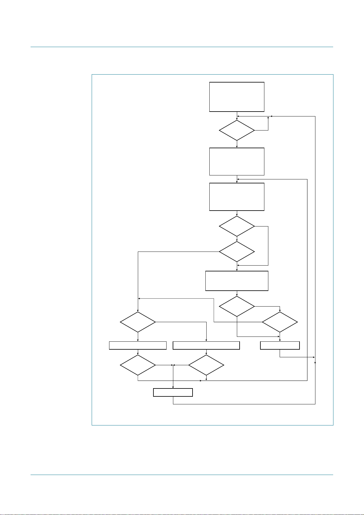
Power on:
Mute, stand-by activated
All other status is random
Complete initialization by
microprocessor is required
Search
upwards?
yes
yes
no
no
no
IF frequency
OK?
Write enable
activated?
yes
Reset bit counter:
Bits are clocked into the
receive register
Completed bytes are written to
the destinastion register
Use value of tuning memory:
Write result to the programmable
divider (also available at the bus)
Wait 10 ms. Have the signal level
available at the bus
Search
Mode?
no
Signal
level OK?
yes
Reset IF counter and enable counting
Wait for result
Have the result available for the bus
Search
Mode?
no
no
yesyes
Add 100 kHz to the tuning memory
Upper
tuning limit
exceeded?
yes
no no
Set 'band limit' flag
Lower
tuning limit
exceeded?
Set 'found' flagSubstract 100 kHz to the tuning memory
001aae346
Fig 3. Flowchart auto search or preset
TEA5767HN_5 © NXP B.V. 2007. All rights reserved.
Product data sheet Rev. 05 — 26 January 2007 9 of 40
Page 10

NXP Semiconductors
Low-power FM stereo radio for handheld applications
8. I2C-bus, 3-wire bus and bus-controlled functions
8.1 I2C-bus specification
TEA5767HN
Information about the I2C-bus can be found in the brochure
it” (order number 9398 393 40011)
The standard I2C-bus specification is expanded by the following definitions:
IC address: 110 0000b
Structure of the I2C-bus logic: slave transceiver
Subaddresses are not used
The maximum LOW-level input and the minimum HIGH-level input are specified to
0.2V
The pin BUSMODE must be connected to ground to operate the IC with the I2C-bus.
Remark: The I2C-bus operates at a maximum clock frequency of 400 kHz. It is not
allowed to connect the IC to an I2C-bus operating at a higher clock rate.
and 0.45V
CCD
8.1.1 Data transfer
Data sequence: address, byte 1, byte 2, byte 3, byte 4 and byte 5 (the data transfer has to
be in this order). The Least Significant Bit (LSB) = 0 of the address indicates a WRITE
operation to the TEA5767HN.
Bit 7 of each byte is considered as the Most Significant Bit (MSB) and has to be
transferred as the first bit of the byte.
The data becomes valid bitwise at the appropriate falling edge of the clock. A STOP
condition after any byte can shorten transmission times.
respectively.
CCD
“The I2C-bus and how to use
.
When writing to the transceiver by using the STOP condition before completion of the
whole transfer:
• The remaining bytes will contain the old information
• If the transfer of a byte is not completed, the new bits will be used, but a new tuning
cycle will not be started
The IC can be switched into a low current Standby mode with the standby bit; the bus is
then still active. The standby current can be reduced by deactivating the bus interface
(pin BUSENABLE LOW). If the bus interface is deactivated (pin BUSENABLE LOW)
without the Standby mode being programmed, the IC maintains normal operation, but is
isolated from the bus lines.
The software programmable output (SWPORT1) can be programmed to operate as a
tuning indicator output. As long as the IC has not completed a tuning action,
pin SWPORT1 remains LOW. The pin becomes HIGH, when a preset or search tuning is
completed or when a band limit is reached.
The reference frequency divider of the synthesizer PLL is changed when the MSB in
byte 5 is set to logic 1. The tuning system can then be clocked via pin XTAL2 at 6.5 MHz.
TEA5767HN_5 © NXP B.V. 2007. All rights reserved.
Product data sheet Rev. 05 — 26 January 2007 10 of 40
Page 11
NXP Semiconductors
8.1.2 Power-on reset
At Power-on reset the mute is set, all other bits are set to LOW.To initialize the IC all bytes
have to be transferred.
8.2 I2C-bus protocol
TEA5767HN
Low-power FM stereo radio for handheld applications
(1)
S
(1) S = START condition.
(2) A = acknowledge.
(3) P = STOP condition.
ADDRESS (WRITE) DATA BYTE(S)
(2)
A
(2)
A
(3)
P
001aae347
Fig 4. Write mode
(1)
S
(1) S = START condition.
(2) A = acknowledge.
ADDRESS (READ) DATA BYTE 1
(2)
A
001aae348
Fig 5. Read mode
Table 4. IC address byte
IC address Mode
[1]
1100000R/
[1] Read or write mode:
a) 0 = write operation to the TEA5767HN.
b) 1 = read operation from the TEA5767HN.
W
TEA5767HN_5 © NXP B.V. 2007. All rights reserved.
Product data sheet Rev. 05 — 26 January 2007 11 of 40
Page 12
NXP Semiconductors
SDA
TEA5767HN
Low-power FM stereo radio for handheld applications
t
f
SCL
t
HD;STA
t
SU;BUSEN
BUSENABLE
tf = fall time of both SDA and SCL signals: 20+ 0.1Cb < tf < 300 ns, where Cb = capacitive load on bus line in pF.
tr = rise time of both SDA and SCL signals: 20 + 0.1Cb < tf < 300 ns, where Cb = capacitive load on bus line in pF.
t
= hold time (repeated) START condition. After this period, the first clock pulse is generated: > 600 ns.
HD;STA
t
= HIGH period of the SCL clock: > 600 ns.
HIGH
t
= LOW period of the SCL clock > 1300 ns.
LOW
t
= set-up time for a repeated START condition: > 600 ns.
SU;STA
t
= data hold time: 300 ns < t
HD;DAT
Remark: 300 ns lower limit is added because the ASIC has no internal hold time for the SDA signal.
t
= data set-up time: t
SU;DAT
t
= set-up time for STOP condition: > 600 ns.
SU;STO
t
= bus free time between a STOP and a START condition: > 600 ns.
BUF
Cb = capacitive load of one bus line: < 400 pF.
t
SU;BUSEN
t
HO;BUSEN
= bus enable set-up time: t
= bus enable hold time: t
Remark: The terms SDA and SCL are the corresponding terms used by the I2C-bus for the DATA and CLOCK signals
respectively.
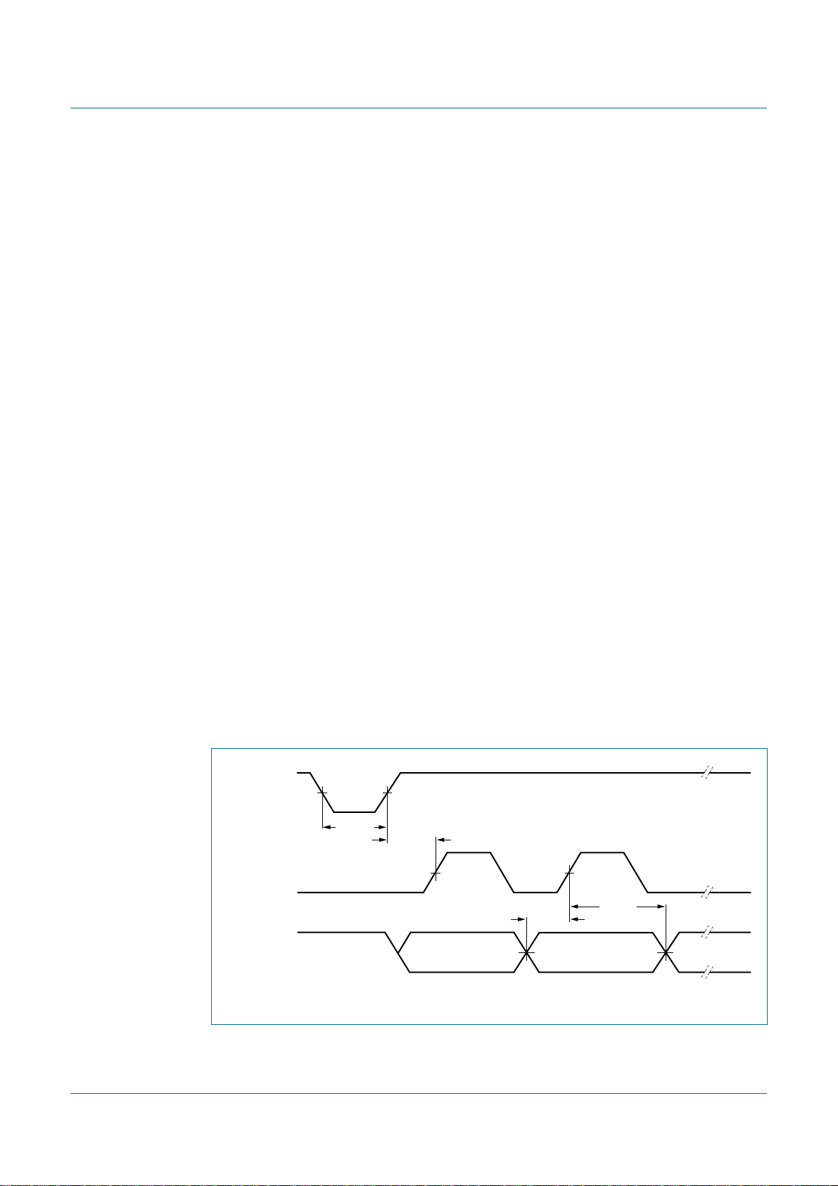
Fig 6. I2C-bus timing diagram
t
HD;DAT
r
t
HD;DAT
< 900 ns.
t
SU;STA
t
HD;STA
t
> 100 ns. If ASIC is used in a standard mode I2C-bus system, t
SU;BUSEN
HO;BUSEN
> 10 µs.
> 10 µs.
t
LOW
SU;DAT
t
HIGH
SU;DAT
t
t
f
t
SU;STO
SU;DAT
BUF
> 250 ns.
t
HO;BUSEN
001aae349
8.3 3-wire bus specification
The 3-wire bus controls the write/read, clock and data lines and operates at a maximum
clock frequency of 400 kHz.
Hint: By using the standby bit the IC can be switched into a low current Standby mode. In
Standby mode the IC must be in the WRITE mode. When the IC is switched to READ
mode, during standby, the IC will hold the data line down. The standby current can be
reduced by deactivating the bus interface (pin BUSENABLE LOW). If the bus interface is
deactivated (pin BUSENABLE LOW) without the Standby mode being programmed, the
IC maintains normal operation, but is isolated from the clock and data line.
8.3.1 Data transfer
Data sequence: byte 1, byte 2, byte 3, byte 4 and byte 5 (the data transfer has to be in this
order).
TEA5767HN_5 © NXP B.V. 2007. All rights reserved.
Product data sheet Rev. 05 — 26 January 2007 12 of 40
Page 13
NXP Semiconductors
A positive edge at pin WRITE/READ enables the data transfer into the IC. The data has to
be stable at the positive edge of the clock. Data maychange while the clock is LOW and is
written into the IC on the positive edge of the clock. Data transfer can be stopped after the
transmission of new tuning information with the first two bytes or after each following byte.
A negative edge at pin WRITE/READ enables the data transfer from the IC. The
WRITE/READ pin changes while the clock is LOW. With the negative edge at
pin WRITE/READ the MSB of the first byte occurs at pin DATA.
The bits are shifted on the negative clock edge to pin DATA and can be read on the
positive edge.
To do two consecutive read or write actions, pin WRITE/READ has to be toggled for at
least one clock period. When a search tuning request is sent, the IC autonomously starts
searching the FM band; the search direction and search stop level can be selected. When
a station with a field strength equal to or greater than the stop level is found, the tuning
system stops and the ready flag bit is set to HIGH. When, during search, a band limit is
reached, the tuning system stops at the band limit and the band limit flag bit is set to
HIGH. The ready flag is also set to HIGH in this case.
TEA5767HN
Low-power FM stereo radio for handheld applications
The software programmable output (SWPORT1) can be programmed to operate as a
tuning indicator output. As long as the IC has not completed a tuning action,
pin SWPORT1 remains LOW. The pin becomes HIGH, when a preset or search tuning is
completed or when a band limit is reached.
The reference frequency divider of the synthesizer PLL is changed when the MSB in
byte 5 is set to logic 1. The tuning system can then be clocked via pin XTAL2 at 6.5 MHz.
8.3.2 Power-on reset
At Power-on reset the mute is set, all other bits are random. To initialize the IC all bytes
have to be transferred.
8.4 Writing data
WRITE_READ
CLOCK
t
W(write)
50 %
t
su(clk)
50 % 50 %
t
su(write)
t
h(write)
DATA
Fig 7. 3-wire bus write data
TEA5767HN_5 © NXP B.V. 2007. All rights reserved.
Product data sheet Rev. 05 — 26 January 2007 13 of 40
50 %
valid data
mhc250
Page 14

NXP Semiconductors
Fig 8. Write mode
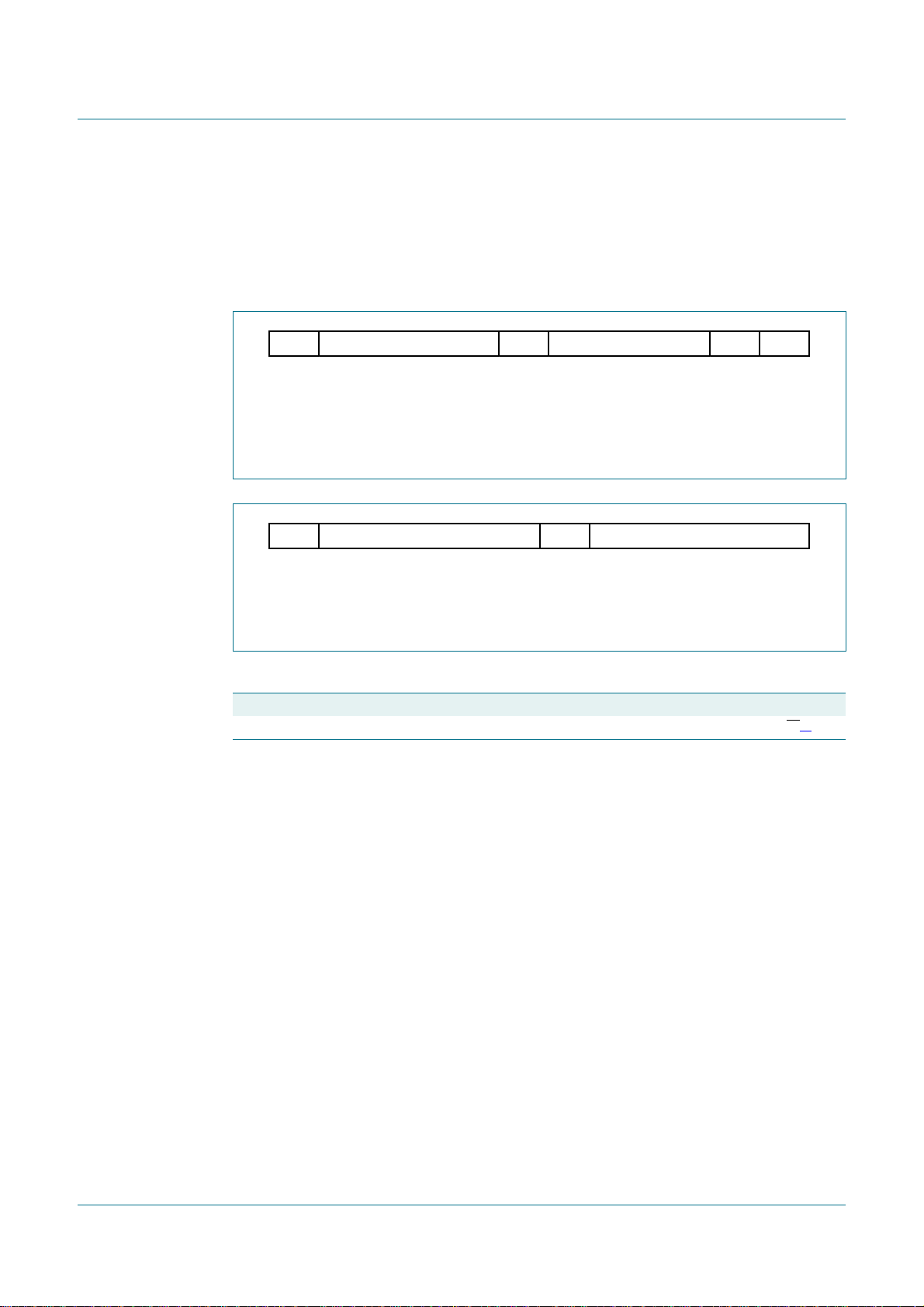
Table 5. Format of 1st data byte
7 (MSB) 6 5 4 3 2 1 0 (LSB)
MUTE SM PLL13 PLL12 PLL11 PLL10 PLL9 PLL8
Table 6. Description of 1st data byte bits
Bit Symbol Description
7 MUTE if MUTE = 1 then L and R audio are muted; if MUTE = 0 then L and R
6SM Search mode: if SM = 1 then in search mode; if SM = 0 then not in
5 to 0 PLL[13:8] setting of synthesizer programmable counter for search or preset
TEA5767HN
Low-power FM stereo radio for handheld applications
DATA BYTE 5DATA BYTE 4DATA BYTE 3DATA BYTE 2DATA BYTE 1
001aae350
audio are not muted
search mode
Table 7. Format of 2nd data byte
7 (MSB) 6 5 4 3 2 1 0 (LSB)
PLL7 PLL6 PLL5 PLL4 PLL3 PLL2 PLL1 PLL0
Table 8. Description of 2nd data byte bits
Bit Symbol Description
7 to 0 PLL[7:0] setting of synthesizer programmable counter for search or preset
Table 9. Format of 3rd data byte
7 (MSB) 6 5 4 3 2 1 0 (LSB)
SUD SSL1 SSL0 HLSI MS MR ML SWP1
Table 10. Description of 3rd data byte bits
Bit Symbol Description
7 SUD Search Up/Down: if SUD = 1 then search up; if SUD = 0 then search
down
6 and 5 SSL[1:0] Search Stop Level: see
4 HLSI High/Low Side Injection: if HLSI = 1 then high side LO injection; if
HLSI = 0 then low side LO injection
3MS Mono to Stereo: if MS = 1 then forced mono; if MS = 0 then stereo
ON
2MR Mute Right: if MR = 1 then the right audio channel is muted and
forced mono; if MR = 0 then the right audio channel is not muted
1ML Mute Left: if ML = 1 then the left audio channel is muted and forced
mono; if ML = 0 then the left audio channel is not muted
0 SWP1 Software programmable port 1: if SWP1 = 1 then port 1 is HIGH; if
SWP1 = 0 then port 1 is LOW
Table 11
TEA5767HN_5 © NXP B.V. 2007. All rights reserved.
Product data sheet Rev. 05 — 26 January 2007 14 of 40
Page 15

NXP Semiconductors
Table 11. Search stop level setting
SSL1 SSL0 Search stop level
0 0 not allowed in search mode
0 1 low; level ADC output = 5
1 0 mid; level ADC output = 7
1 1 high; level ADC output = 10
Table 12. Format of 4th data byte
7 (MSB) 6 5 4 3 2 1 0 (LSB)
SWP2 STBY BL XTAL SMUTE HCC SNC SI
Table 13. Description of 4th data byte bits
Bit Symbol Description
7 SWP2 Software programmable port 2: if SWP2 = 1 then port 2 is HIGH; if
6 STBY Standby: if STBY = 1 then in Standby mode; if STBY = 0 then not in
5BL Band Limits: if BL = 1 then Japanese FM band; if BL = 0 then
4XTAL Clock frequency: see
3 SMUTE Soft Mute: if SMUTE = 1 then soft mute is ON; if SMUTE = 0 then soft
2 HCC High Cut Control: if HCC = 1 then high cut control is ON; if HCC = 0
1 SNC Stereo Noise Cancelling: if SNC = 1 then stereo noise cancelling is
0SI Search Indicator: if SI = 1 then pin SWPORT1 is output for the ready
TEA5767HN
Low-power FM stereo radio for handheld applications
SWP2 = 0 then port 2 is LOW
Standby mode
US/Europe FM band
Table 16
mute is OFF
then high cut control is OFF
ON; if SNC = 0 then stereo noise cancelling is OFF
flag; if SI = 0 then pin SWPORT1 is software programmable port 1
Table 14. Format of 5th data byte
7 (MSB) 6 5 4 3 2 1 0 (LSB)
PLLREF DTC - - - - - -
Table 15. Description of 5th data byte bits
Bit Symbol Description
7 PLLREF if PLLREF = 1 then the 6.5 MHz reference frequency for the PLL is
enabled; if PLLREF = 0 then the 6.5 MHz reference frequency for the
PLL is disabled; see
6 DTC if DTC = 1 then the de-emphasis time constant is 75 µs; if DTC = 0
then the de-emphasis time constant is 50 µs
5 to 0 - not used; position is don’t care
TEA5767HN_5 © NXP B.V. 2007. All rights reserved.
Product data sheet Rev. 05 — 26 January 2007 15 of 40
Table 16
Page 16

NXP Semiconductors
Table 16. Clock bits setting
PLLREF XTAL Clock frequency
0 0 13 MHz
0 1 32.768 kHz
1 0 6.5 MHz
1 1 not allowed
8.5 Reading data
TEA5767HN
Low-power FM stereo radio for handheld applications
WRITE_READ
CLOCK
DATA
t
W(read)
50 %
t
su(clk)
t
HIGH
50 % 50 %
t
LOW
t
h
50 % 50 %
t
d
mhc249
Fig 9. 3-wire bus read data
DATA BYTE 5DATA BYTE 4DATA BYTE 3DATA BYTE 2DATA BYTE 1
001aae350
Fig 10. Read mode
Table 17. Format of 1st data byte
7 (MSB) 6 5 4 3 2 1 0 (LSB)
RF BLF PLL13 PLL12 PLL11 PLL10 PLL9 PLL8
Table 18. Description of 1st data byte bits
Bit Symbol Description
7RF Ready Flag: if RF = 1 then a station has been found or the band limit
has been reached; if RF = 0 then no station has been found
6 BLF Band Limit Flag: if BLF = 1 then the band limit has been reached; if
BLF = 0 then the band limit has not been reached
5 to 0 PLL[13:8] setting of synthesizer programmable counter after search or preset
Table 19. Format of 2nd data byte
7 (MSB) 6 5 4 3 2 1 0 (LSB)
PLL7 PLL6 PLL5 PLL4 PLL3 PLL2 PLL1 PLL0
TEA5767HN_5 © NXP B.V. 2007. All rights reserved.
Product data sheet Rev. 05 — 26 January 2007 16 of 40
Page 17

NXP Semiconductors
Table 20. Description of 2nd data byte bits
Bit Symbol Description
7 to 0 PLL[7:0] setting of synthesizer programmable counter after search or preset
Table 21. Format of 3rd data byte
7 (MSB) 6 5 4 3 2 1 0 (LSB)
STEREO IF6 IF5 IF4 IF3 IF2 IF1 IF0
Table 22. Description of 3rd data byte bits
Bit Symbol Description
7 STEREO Stereo indication: if STEREO = 1 then stereo reception; if
6 to 0 PLL[13:8] IF counter result
Table 23. Format of 4th data byte
7 (MSB) 6 5 4 3 2 1 0 (LSB)
LEV3 LEV2 LEV1 LEV0 CI3 CI2 CI1 0
TEA5767HN
Low-power FM stereo radio for handheld applications
STEREO = 0 then mono reception
Table 24. Description of 4th data byte bits
Bit Symbol Description
7 to 4 LEV[3:0] level ADC output
3 to 1 CI[3:1] Chip Identification: these bits have to be set to logic 0
0 - this bit is internally set to logic 0
Table 25. Format of 5th data byte
7 (MSB) 6 5 4 3 2 1 0 (LSB)
00000000
Table 26. Description of 5th data byte bits
Bit Symbol Description
7 to 0 - reserved for future extensions; these bits are internally set to logic 0
TEA5767HN_5 © NXP B.V. 2007. All rights reserved.
Product data sheet Rev. 05 — 26 January 2007 17 of 40
Page 18

NXP Semiconductors
9. Internal circuitry
Table 27. Internal circuitry
Pin Symbol Equivalent circuit
1 n.c.
2 CPOUT
TEA5767HN
Low-power FM stereo radio for handheld applications
270 Ω
3V
4V
5V
COTANK1
COTANK2
CC(VCO)
6 DGND
7V
CCD
8 DATA
120 Ω
8
2
4
3
120 Ω
mhc286
6
mhc287
mhc285
9 CLOCK
270 Ω
69
mhc288
10 n.c.
TEA5767HN_5 © NXP B.V. 2007. All rights reserved.
Product data sheet Rev. 05 — 26 January 2007 18 of 40
Page 19

NXP Semiconductors
Table 27. Internal circuitry
Pin Symbol Equivalent circuit
11 WRITE/READ
12 BUSMODE
TEA5767HN
Low-power FM stereo radio for handheld applications
270 Ω
611
mhc289
270 Ω
612
mhc290
13 BUSENABLE
14 SWPORT1
15 SWPORT2
16 XTAL1
17 XTAL2
150 Ω
613
mhc291
150 Ω
14
6
6
150 Ω
mhc292
15
mhc293
16 17
mhc294
TEA5767HN_5 © NXP B.V. 2007. All rights reserved.
Product data sheet Rev. 05 — 26 January 2007 19 of 40
Page 20

NXP Semiconductors
Table 27. Internal circuitry
Pin Symbol Equivalent circuit
18 PHASEFIL
19 PILFIL
TEA5767HN
Low-power FM stereo radio for handheld applications
18
33
mhc295
270 Ω
19
20 n.c.
21 n.c.
22 V
23 V
AFL
AFR
24 TMUTE
33
mhc296
10 Ω
22
33
mhc297
10 Ω
23
33
mhc298
24
1 kΩ
33
mhc299
TEA5767HN_5 © NXP B.V. 2007. All rights reserved.
Product data sheet Rev. 05 — 26 January 2007 20 of 40
Page 21

NXP Semiconductors
Table 27. Internal circuitry
Pin Symbol Equivalent circuit
25 MPXO
TEA5767HN
Low-power FM stereo radio for handheld applications
150 Ω
25
33
mhc300
26 V
ref
27 TIFC
28 LIMDEC1
26
mhc301
270 Ω
40 kΩ
33
27
mhc302
28
mhc303
29 LIMDEC2
270 Ω
29
mhc304
30 n.c.
31 n.c.
TEA5767HN_5 © NXP B.V. 2007. All rights reserved.
Product data sheet Rev. 05 — 26 January 2007 21 of 40
Page 22

NXP Semiconductors
Table 27. Internal circuitry
Pin Symbol Equivalent circuit
32 I
33 AGND
34 V
35 RFI1
36 RFGND
37 RFI2
TEA5767HN
Low-power FM stereo radio for handheld applications
gain
32
mhc305
CCA
35 37
38 TAGC
39 LOOPSW
40 n.c.
10. Limiting values
Table 28. Limiting values
In accordance with the Absolute Maximum Rating System (IEC 60134).
Symbol Parameter Conditions Min Max Unit
V
VCOTANK1
V
VCOTANK2
V
CCD
V
CCA
T
stg
T
amb
36
38
36
5
39
VCO tuned circuit output
mhc306
mhc307
mhc308
−0.3 +8 V
voltage 1
VCO tuned circuit output
−0.3 +8 V
voltage 2
digital supply voltage −0.3 +5 V
analog supply voltage −0.3 +8 V
storage temperature −55 +150 °C
ambient temperature −10 +75 °C
TEA5767HN_5 © NXP B.V. 2007. All rights reserved.
Product data sheet Rev. 05 — 26 January 2007 22 of 40
Page 23

NXP Semiconductors
TEA5767HN
Low-power FM stereo radio for handheld applications
Table 28. Limiting values
…continued
In accordance with the Absolute Maximum Rating System (IEC 60134).
Symbol Parameter Conditions Min Max Unit
V
esd
electrostatic discharge
voltage
[1] Machine model (R = 0 Ω, C = 200 pF).
[2] Human body model (R = 1.5 kΩ, C = 100 pF).
all pins except
pin DATA
pin DATA
[1]
−200 +200 V
[2]
−2000 +2000 V
[1]
−150 +200 V
[2]
−2000 +2000 V
11. Thermal characteristics
Table 29. Thermal characteristics
Symbol Parameter Conditions Typ Unit
R
th(j-a)
thermal resistance from junction to
in free air 29 K/W
ambient
12. Static characteristics
Table 30. Static characteristics
V
CCA=VCC(VCO)=VCCD
Symbol Parameter Conditions Min Typ Max Unit
Supply voltages
V
CCA
V
CC(VCO)
V
CCD
analog supply voltage 2.5 3.0 5.0 V
VCO supply voltage 2.5 3.0 5.0 V
digital supply voltage 2.5 3.0 5.0 V
Supply currents
I
CCA
I
CC(VCO)
analog supply current operating
VCO supply current operating
[1]
= 2.7 V; T
=25°C; All AC values are given in RMS unless otherwise specified.
amb
= 3 V 6.0 8.4 10.5 mA
V
CCA
= 5 V 6.2 8.6 10.7 mA
V
CCA
Standby mode
=3V - 3 6 µA
V
CCA
= 5 V - 3.2 6.2 µA
V
CCA
V
CC(VCO)
V
CC(VCO)
= 3 V 560 750 940 µA
= 5 V 570 760 950 µA
Standby mode
V
CC(VCO)
V
CC(VCO)
=3V - 1 2 µA
= 5 V - 1.2 2.2 µA
TEA5767HN_5 © NXP B.V. 2007. All rights reserved.
Product data sheet Rev. 05 — 26 January 2007 23 of 40
Page 24

NXP Semiconductors
TEA5767HN
Low-power FM stereo radio for handheld applications
Table 30. Static characteristics
V
CCA=VCC(VCO)=VCCD
= 2.7 V; T
…continued
=25°C; All AC values are given in RMS unless otherwise specified.
amb
Symbol Parameter Conditions Min Typ Max Unit
I
CCD
digital supply current operating
V
CCD
V
CCD
Standby mode; V
= 3 V 2.1 3.0 3.9 mA
= 5 V 2.25 3.15 4.05 mA
=3V
CCD
bus enable line HIGH 30 56 80 µA
bus enable line LOW 11 19 26 µA
Standby mode; V
CCD
=5V
bus enable line HIGH 50 78 105 µA
bus enable line LOW 20 33 45 µA
[1] V
CCA
, V
CC(VCO)
and V
must not differ by more than 200 mV.
CCD
Table 31. DC operating points, unloaded DC voltage
V
=
V
CCA
Operating
CC(VCO)=VCCD
Conditions Min Typ Max Unit
= 2.7 V; T
=25°C; unless otherwise specified.
amb
point
V
CPOUT
V
XTAL2
0.1 - V
CC(VCO)
data byte 4 bit 4 = 1 1.64 1.72 1.8 V
− 0.1 V
data byte 4 bit 4 = 0 1.68 1.75 1.82 V
V
XTAL2
data byte 4 bit 4 = 1 1.64 1.72 1.8 V
data byte 4 bit 4 = 0 1.68 1.75 1.82 V
V
PHASEFIL
V
PILFIL
V
AFL
V
AFR
V
TMUTE
V
MPXO
V
ref
V
TIFC
V
LIMDEC1
V
LIMDEC2
V
Igain
V
RFI1
V
RFI2
V
TAGC
0.4 1.2 V
0.65 0.9 1.3 V
fRF= 98 MHz; VRF= 1 mV 720 850 940 mV
fRF= 98 MHz; VRF= 1 mV 720 850 940 mV
VRF= 0 V 1.5 1.65 1.8 V
fRF= 98 MHz; VRF= 1 mV 680 815 950 mV
1.45 1.55 1.65 V
1.34 1.44 1.54 V
1.86 1.98 2.1 V
1.86 1.98 2.1 V
480 530 580 mV
0.93 1.03 1.13 V
0.93 1.03 1.13 V
VRF= 0 V 1 1.57 2 V
− 0.4 V
CCA
TEA5767HN_5 © NXP B.V. 2007. All rights reserved.
Product data sheet Rev. 05 — 26 January 2007 24 of 40
Page 25

NXP Semiconductors
TEA5767HN
Low-power FM stereo radio for handheld applications
13. Dynamic characteristics
Table 32. Dynamic characteristics
V
CCA=VCCD=VCC(VCO)
For V
the emf value is given; unless otherwise specified.
RF
Symbol Parameter Conditions Min Typ Max Unit
VCO
f
osc
oscillator frequency 150 - 217 MHz
Crystal oscillator
Circuit input: pin XTAL2
V
R
C
i(osc)
i
i
oscillator input voltage oscillator externally clocked 140 - 350 mV
input resistance oscillator externally clocked
input capacitance oscillator externally clocked
Crystal: 32.768 kHz
f
r
series resonance
frequency
∆f/f
r
C
0
R
S
∆f
r/fr(25 °C)
frequency deviation −20 × 10−6- +20 × 10
shunt capacitance - - 3.5 pF
series resistance - - 80 kΩ
temperature drift −10 °C<T
Crystal: 13 MHz
f
r
series resonance
frequency
∆f/f
r
C
0
C
mot
R
S
∆f
r/fr(25 °C)
frequency deviation −30 × 10−6- +30 × 10
shunt capacitance - - 4.5 pF
motional capacitance 1.5 - 3.0 fF
series resistance - - 100 kΩ
temperature drift −40 °C<T
Synthesizer
Programmable divider
N
prog
programmable divider
ratio
∆N
step
programmable divider
step size
Reference frequency divider
N
ref
crystal oscillator divider
ratio
= 2.7 V; T
[1]
=25°C; AC values given in RMS;
amb
data byte 4 bit 4 = 0 2 3 4 kΩ
data byte 4 bit 4 = 1 230 330 430 kΩ
data byte 4 bit 4 = 0 3.9 5.6 7.3 pF
data byte 4 bit 4 = 1 5 6 7 pF
data byte 4 bit 4 = 1 - 32.768 - kHz
< +60 °C −50 × 10−6- +50 × 10
amb
data byte 4 bit 4 = 0 - 13 - MHz
< +85 °C −30 × 10−6- +30 × 10
amb
data byte 1 = XX11 1111;
- - 8191 -
data byte 2 = 1111 1110
data byte 1 = XX01 0000;
2048 - - -
data byte 2 = 0000 0000
-1--
data byte 4 bit 4 = 0 - 260 - data byte 5 bit 7 = 1;
- 130 - -
data byte 4 bit 4 = 0
data byte 4 bit 4 = 1 - 1 - -
−6
−6
−6
−6
TEA5767HN_5 © NXP B.V. 2007. All rights reserved.
Product data sheet Rev. 05 — 26 January 2007 25 of 40
Page 26

NXP Semiconductors
TEA5767HN
Low-power FM stereo radio for handheld applications
Table 32. Dynamic characteristics
V
CCA=VCCD=VCC(VCO)
For V
the emf value is given; unless otherwise specified.
RF
= 2.7 V; T
…continued
=25°C; AC values given in RMS;
amb
Symbol Parameter Conditions Min Typ Max Unit
Charge pump: pin CPOUT
I
sink
I
source
charge pump peak sink
current
chargepump peak source
current
0.2 V < V
V
VCOTANK2
f
VCO>fref
0.2 V < V
V
VCOTANK2
f
VCO<fref
CPOUT
− 0.2 V;
× N
CPOUT
− 0.2 V;
× N
prog
prog
<
<
- 0.5 - µA
- −0.5 - µA
IF counter
V
RF
RF input voltage for
-1218µV
correct IF count
N
IF
N
precount
T
count(IF)
RES
IF
count
count(IF)
IF counter length - 7 - bit
IF counter prescaler ratio - 64 - -
IF counter period f
IF counter resolution f
IF counter result for
search tuning stop
= 32.768 kHz - 15.625 - ms
xtal
= 13 MHz - 15.754 - ms
f
xtal
= 32.768 kHz - 4.096 - kHz
xtal
= 13 MHz - 4.0625 - kHz
f
xtal
f
= 32.768 kHz 29h - 3Dh -
xtal
= 13 MHz 30h - 3Dh -
f
xtal
Pins DATA, CLOCK, WRITE/READ, BUSMODE and BUSENABLE
R
i
input resistance 10 - - MΩ
TEA5767HN_5 © NXP B.V. 2007. All rights reserved.
Product data sheet Rev. 05 — 26 January 2007 26 of 40
Page 27

NXP Semiconductors
TEA5767HN
Low-power FM stereo radio for handheld applications
Table 32. Dynamic characteristics
V
CCA=VCCD=VCC(VCO)
For V
the emf value is given; unless otherwise specified.
RF
= 2.7 V; T
…continued
=25°C; AC values given in RMS;
amb
Symbol Parameter Conditions Min Typ Max Unit
Software programmable ports
Pin SWPORT1
I
sink(max)
maximum sink current data byte 3 bit 0 = 0;
500 - - µA
data byte 4 bit 0 = 0;
I
leak(max)
V
SWPORT1
maximum leakage current data byte 3 bit 0 = 1;
V
SWPORT1
< 0.5 V
−1- +1µA
<5V
Pin SWPORT2
I
sink(max)
I
leak(max)
maximum sink current data byte 4 bit 7 = 0;
V
SWPORT1
< 0.5 V
maximum leakage current data byte 4 bit 7 = 1;
V
SWPORT1
<5V
500 - - µA
−1- +1µA
FM signal channel
FM RF input
f
FM(ant)
R
i
FM input frequency 76 - 108 MHz
input resistance at pins
75 100 125 Ω
RFI1 and RFI2 to RFGND
C
i
input capacitance at pins
2.5 4 6 pF
RFI1 and RFI2 to RFGND
V
RF
RF sensitivity input
voltage
fRF= 76 MHz to 108 MHz;
∆f = 22.5 kHz; f
mod
= 1 kHz;
- 2 3.5 µV
(S+N)/N = 26 dB; L = R;
de-emphasis = 75 µs;
B
= 300 Hz to 15 kHz
AF
IP3
IP3
in
out
in-band 3rd-order
intercept point related to
V
RFI1-RFI2
(peak value)
out-band 3rd-order
intercept point related to
V
RFI1-RFI2
(peak value)
= 200 kHz; ∆f2= 400 kHz;
∆f
1
f
= 76 MHz to 108 MHz
tune
= 4 MHz; ∆f2= 8 Hz;
∆f
1
f
= 76 MHz to 108 MHz
tune
81 84 - dBµV
82 85 - dBµV
RF AGC
V
RF1
RF input voltage for start
of AGC
f
= 93 MHz; f
RF1
=50dBµV;
V
RF2
V
∆
TMUTE
------------------------
V
RF1
RF2
14 mV
<
-------------------
3 dBµV
= 98 MHz;
[2]
66 72 78 dBµV
IF filter
f
B
S
S
S
IF
IF
+200
−200
+100
IF filter center frequency 215 225 235 kHz
IF filter bandwidth 85 94 102 kHz
high side 200 kHz
selectivity
low side 200 kHz
selectivity
high side 100 kHz
selectivity
∆f = +200 kHz;
f
= 76 MHz to 108 MHz
tune
∆f=−200 kHz;
f
= 76 MHz to 108 MHz
tune
∆f = +100 kHz;
f
= 76 MHz to 108 MHz
tune
[3]
39 43 - dB
[3]
32 36 - dB
[3]
812- dB
TEA5767HN_5 © NXP B.V. 2007. All rights reserved.
Product data sheet Rev. 05 — 26 January 2007 27 of 40
Page 28

NXP Semiconductors
TEA5767HN
Low-power FM stereo radio for handheld applications
Table 32. Dynamic characteristics
V
CCA=VCCD=VCC(VCO)
For V
the emf value is given; unless otherwise specified.
RF
= 2.7 V; T
…continued
=25°C; AC values given in RMS;
amb
Symbol Parameter Conditions Min Typ Max Unit
S
-100
low side 100 kHz
selectivity
IR image rejection f
∆f=−100 kHz;
f
= 76 MHz to 108 MHz
tune
= 76 MHz to 108 MHz;
tune
V
=50dBµV
RF
[3]
812- dB
24 30 - dB
FM IF level detector and mute voltage
V
RF
RF input voltage for start
read mode data byte 4 bit 4 = 1 2 3 5 µV
of level ADC
∆V
step
level ADC step size 2 3 5 dB
Pin TMUTE
V
level
V
level(slope)
R
o
level output DC voltage VRF=0µV 1.55 1.65 1.80 V
=3µV 1.60 1.70 1.85 V
V
RF
slope of level voltage VRF=10µV to 500 µV 150 165 180
--------------
20 dB
output resistance 280 400 520 kΩ
FM demodulator: pin MPXO
V
MPXO
demodulator output
voltage
VRF=1mV; L=R;
∆f = 22.5 kHz; f
mod
= 1 kHz;
60 75 90 mV
de-emphasis = 75 µs;
B
= 300 Hz to 15 kHz
AF
(S+N)/N maximum signal plus
noise-to-noise ratio
V
=1mV; L=R;
RF
∆f = 22.5 kHz; f
mod
54 60 - dB
= 1 kHz;
de-emphasis = 75 µs;
B
= 300 Hz to 15 kHz
AF
THD total harmonic distortion V
=1mV; L=R;
RF
∆f = 75 kHz; f
mod
- 0.5 1.5 %
= 1 kHz;
de-emphasis = 75 µs
α
AM
AM suppression VRF= 300 µV; L=R;
∆f = 22.5 kHz; f
mod
= 1 kHz;
40 - - dB
m = 0.3; de-emphasis = 75 µs;
B
= 300 Hz to 15 kHz
AF
R
o
demodulator output
- - 500 Ω
resistance
I
sink
demodulator output sink
--30µA
current
Soft mute
V
α
RF
mute
RF input voltage for soft
mute start
mute attenuation VRF=1µV; L=R;
α
= 3 dB; data byte 4
mute
bit 3 = 1
∆f = 22.5 kHz; f
mod
3510µV
4 7 15 dB
= 1 kHz;
de-emphasis = 75 µs;
B
= 300 Hz to 15 kHz;
AF
data byte 4 bit 3 = 1
mV
TEA5767HN_5 © NXP B.V. 2007. All rights reserved.
Product data sheet Rev. 05 — 26 January 2007 28 of 40
Page 29

NXP Semiconductors
TEA5767HN
Low-power FM stereo radio for handheld applications
Table 32. Dynamic characteristics
V
CCA=VCCD=VCC(VCO)
For V
the emf value is given; unless otherwise specified.
RF
= 2.7 V; T
…continued
=25°C; AC values given in RMS;
amb
Symbol Parameter Conditions Min Typ Max Unit
MPX decoder
V
AFL
left audio frequency
output voltage
VRF=1mV; L=R;
∆f = 22.5 kHz; f
mod
60 75 90 mV
= 1 kHz;
de-emphasis = 75 µs
V
AFR
right audio frequency
output voltage
VRF=1mV; L=R;
∆f = 22.5 kHz; f
mod
60 75 90 mV
= 1 kHz;
de-emphasis = 75 µs
R
AFL
left audio frequency
--50Ω
output resistance
R
AFR
right audio frequency
--50Ω
output resistance
I
sink(AFL)
left audio frequency
170 - - µA
output sink current
I
sink(AFR)
right audio frequency
170 - - µA
output sink current
V
MPXIN(max)
V
AFL
input overdrive margin THD < 3 % 4 - - dB
left audio frequency
output voltage difference
VRF=1mV; L=R;
∆f = 75 kHz; f
mod
-1-+1dB
= 1 kHz;
de-emphasis = 75 µs
V
AFR
right audio frequency
output voltage difference
VRF=1mV; L=R;
∆f = 75 kHz; f
mod
-1-+1dB
= 1 kHz;
de-emphasis = 75 µs
α
cs(stereo)
stereo channel separation VRF=1mV;R=L=0orR=0
24 30 - dB
and L = 1 including 9 % pilot;
∆f = 75 kHz; f
mod
= 1 kHz;
data byte 3 bit 3 = 0;
data byte 4 bit 1 = 1
(S+N)/N maximum signal plus
noise-to-noise ratio
V
=1mV; L=R;
RF
∆f = 22.5 kHz; f
mod
= 1 kHz;
54 60 - dB
de-emphasis = 75 µs;
B
= 300 Hz to 15 kHz
AF
THD total harmonic distortion V
=1mV; L=R;
RF
∆f = 75 kHz; f
mod
- 0.4 1 %
= 1 kHz;
de-emphasis = 75 µs
α
∆f
pilot
pilot
pilot suppression
measured at pins V
and V
AFR
AFL
stereo pilot frequency
deviation
related to ∆f = 75 kHz;
f
= 1 kHz;
mod
40 50 - dB
de-emphasis = 75 µs
VRF= 1 mV; read mode
data byte 3 bit 7 = 1 - 3.6 5.8 kHz
data byte 3 bit 7 = 0 1 3 - kHz
f
∆
pilot1
---------------- -
f
∆
pilot2
pilot switch hysteresis V
= 1 mV 2 - - dB
RF
TEA5767HN_5 © NXP B.V. 2007. All rights reserved.
Product data sheet Rev. 05 — 26 January 2007 29 of 40
Page 30

NXP Semiconductors
TEA5767HN
Low-power FM stereo radio for handheld applications
Table 32. Dynamic characteristics
V
CCA=VCCD=VCC(VCO)
For V
the emf value is given; unless otherwise specified.
RF
= 2.7 V; T
…continued
=25°C; AC values given in RMS;
amb
Symbol Parameter Conditions Min Typ Max Unit
High cut control
TC
de-em
de-emphasis time
constant
VRF=1mV
data byte 5 bit 6 = 0 38 50 62 µs
data byte 5 bit 6 = 1 57 75 93 µs
=1µV
V
RF
data byte 5 bit 6 = 0 114 150 186 µs
data byte 5 bit 6 = 1 171 225 279 µs
Mono to stereo blend control
α
cs(stereo)
stereo channel separation VRF=45µV; R = L = 0 or
41016dB
R = 0 and L = 1 including 9 %
pilot; ∆f = 75 kHz; f
mod
= 1 kHz;
data byte 3 bit 3 = 0;
data byte 4 bit 1 = 1
Mono to stereo switched
α
cs(stereo)
stereochannel separation
switching from mono to
stereo with increasing RF
input level
R = L = 0 or R = 0 and L = 1
including 9 % pilot;
∆f = 75 kHz; f
mod
= 1 kHz;
data byte 3 bit 3 = 0;
data byte 4 bit 1 = 0
V
= 1 mV 24 - - dB
RF
=20µV--1dB
V
RF
Bus-driven mute functions
Tuning mute
α
mute
V
AFL
and V
AFR
muting
data byte 1 bit 7 = 1 - - −60 dB
depth
V
α
mute(L)
α
mute(R)
muting depth data byte 3 bit 1 = 1;
AFL
V
muting depth data byte 3 bit 2 = 1;
AFR
f
= 1 kHz; R
AF
f
= 1 kHz; R
AF
load(L)
load(R)
--−80 dB
<30kΩ
--−80 dB
<30kΩ
[1] Calculation of this 14-bit word can be done as follows:
formula for high side injection: ; formula for low side injection:
where:
N = decimal value of PLL word;
f
= the wanted tuning frequency [Hz];
RF
fIF= the intermediate frequency [Hz] = 225 kHz;
f
= the reference frequency [Hz] = 32.768 kHz for the 32.768 kHz crystal; f
ref
clocked with 6.5 MHz.
Example for receiving a channel at 100 MHz with high side injection:
The PLL word becomes 2FCAh.
[2] VRF in Figure 13 is replaced by V
[3] Low side and high side selectivity can be switched by changing the mixer from high side to low side LO injection.
TEA5767HN_5 © NXP B.V. 2007. All rights reserved.
Product data sheet Rev. 05 — 26 January 2007 30 of 40
N
= N
---------------------------------------
f
ref
= 50 kHz for the 13 MHz crystal or when externally
ref
4 100 106× 225 10×
N
--------------------------------------------------------------------
RF1+VRF2
. The radio is tuned to 98 MHz (high side injection).
4fRFfIF+()×
4fRFfIF–()×
=
-------------------------------------- -
+()×
32768
f
ref
3
12234==
Page 31

NXP Semiconductors
14. FM characteristics
TEA5767HN
Low-power FM stereo radio for handheld applications
0
V
AFL,
AFR
−20
−40
−60
−80
(1)
−1
10
110
10
V
(dB)
(1) Mono signal, no soft mute, ∆f = 22,5 kHz.
(2) Noise in mono mode, no soft mute.
(3) Total Harmonic Distortion (THD), ∆f = 75 kHz.
Fig 11. FM mono characteristics
V
V
(dB)
0
AFL,
AFR
−20
(1)
(2)
001aae351
(2)
(3)
2
3
10
4
10
5
10
VRF (µV)
001aae352
10
4
THD+N
(%)
3
2
1
0
6
4
THD+N
(%)
3
−40
−60
−80
(3)
(4)
−1
10
110
10
2
3
10
4
10
5
10
VRF (µV)
2
1
0
6
10
(1) Right channel with modulation right, SNC on, ∆f = 67,5 kHz + 6,75 kHz pilot.
(2) Left channel with modulation left, SNC on, ∆f = 67,5 kHz + 6,75 kHz pilot.
(3) Noise in stereo mode, SNC on, ∆f = 0 kHz + 6,75 kHz pilot.
(4) Total Harmonic Distortion (THD), ∆f = 67,5 kHz + 6,75 kHz pilot.
Fig 12. FM stereo characteristics
TEA5767HN_5 © NXP B.V. 2007. All rights reserved.
Product data sheet Rev. 05 — 26 January 2007 31 of 40
Page 32

NXP Semiconductors
15. I2C-bus characteristics
Table 33. Digital levels and timing
Symbol Parameter Conditions Min Max Unit
Digital inputs
V
IH
V
IL
Digital outputs
I
sink(L)
V
OL
Timing
f
clk
t
HIGH
t
LOW
t
W(write)
t
W(read)
t
su(clk)
t
h(out)
t
d(out)
t
su(write)
t
h(write)
HIGH-level input voltage 0.45V
LOW-level input voltage - 0.2V
LOW-level sink current 500 - µA
LOW-level output voltage IOL= 500 µA - 450 mV
clock input frequency I2C-bus enabled - 400 kHz
clock HIGH time I2C-bus enabled 1 - µs
clock LOW time I2C-bus enabled 1 - µs
pulse width for write enable 3-wire bus enabled 1 - µs
pulse width for read enable 3-wire bus enabled 1 - µs
clock set-up time 3-wire bus enabled 300 - ns
read mode data output hold time 3-wire bus enabled 10 - ns
read mode output delay time 3-wire bus enabled - 400 ns
write mode set-up time 3-wire bus enabled 100 - ns
write mode hold time 3-wire bus enabled 100 - ns
TEA5767HN
Low-power FM stereo radio for handheld applications
-V
CCD
V
CCD
3-wire bus enabled - 400 kHz
3-wire bus enabled 1 - µs
3-wire bus enabled 1 - µs
16. Test information
Table 34. Component list for Figure 1 and Figure 13
Component Parameter Value Tolerance Type Manufacturer
R1 resistor with low
temperature coefficient
D1 and D2 varicap for VCO tuning - - BB202 Philips
L1 RF band filter coil 120 nH ±2% Q
L2 and L3 VCO coil 33 nH ±2% Q
XTAL13MHz 13 MHz crystal - - NX4025GA
C
pull
pulling capacitor for
NX4025GA
XTAL32768Hz 32,768 kHz crystal - C
pull
pulling capacitor for
XTAL32768Hz
[1] Value of the C
TEA5767HN_5 © NXP B.V. 2007. All rights reserved.
Product data sheet Rev. 05 — 26 January 2007 32 of 40
must be as close as possible to the value of C
pull
18 kΩ±1 % RC12G Philips
=40
min
=40
min
10 pF -
[1]
C
load
-
of the crystal.
load
Page 33

TEA5767HN_5 © NXP B.V. 2007. All rights reserved.
Product data sheet Rev. 05 — 26 January 2007 33 of 40
xxxxxxxxxxxxxxxxxxxxx xxxxxxxxxxxxxxxxxxxxxxxxxx xxxxxxx x x x xxxxxxxxxxxxxxxxxxxxxxxxxxxxxx xxxxxxxxxxxxxxxxxxx xx xx
xxxxx xxxxxxxxxxxxxxxxxxxxxxxxxxx xxxxxxxxxxxxxxxxxxx xxxxxx xxxxxxxxxxxxxxxxxxxxxxxxxxxxxxxxxxx xxxxxxxxxxxx x x
xxxxxxxxxxxxxxxxxxxxx xxxxxxxxxxxxxxxxxxxxxxxxxxxxxx xxxxx xxxxxxxxxxxxxxxxxxxxxxxxxxxxxxxxxxxxxxxxxxxxxxxxxx xxxxxxxx
xxxxxxxxxxxxxxxxxxxxxxxxx xxxxxxxxxxxxxxxxxxxx xxx
NXP Semiconductors
47 nF 47 nF 33 nF
LIMDEC2
29 28 27 26 25
R1
22 nF
V
CCA
4.7 Ω
100 pF
40 Ω
L1
V
RF
27 pF
47 pF
22 µF
4.7 nF
LOOPSW
I
gain
AGND
V
CCA
RFI1
RFGND
RFI2
TAGC
32
33
34
I/Q-MIXER
1st FM
35
36
37
38
39
TUNING SYSTEM
23
CPOUT VCOTANK2 V
39 nF10 nF
10 kΩ
100 kΩ
AGC
VCO
VCOTANK1
D1L3D2
2
N1
L2
GAIN
STABILIZATION
RESONANCE
AMPLIFIER
IF CENTRE
FREQUENCY
ADJUST
programmable divider output
reference frequency divider output
45
CC(VCO)
LIMDEC1 TIFC V
LIMITER
LEVEL
ADC
6789
DGND CLOCK
12 Ω
V
CCD
47 nF
DEMODULATOR
COUNTER
I
ref
MUX
2
I
C-BUS
AND
3-WIRE BUS
CCD
22 nF
IF
TEA5767HN
PROGRAMMABLE
DATAV
ref
POWER
SUPPLY
SOFTWARE
PORT
pilot
mono
MPXO TMUTE
SOFT
MUTE
MPX
DECODER
1, 10, 20, 21,
30, 31, 40
n.c.
33 nF
V
AFR
24 23 22
SDS
CRYSTAL
OSCILLATOR
mhc284
V
AFL
19
18
17
16
15
14
13
12
11
PILFIL
33 kΩ
PHASEFIL
XTAL2
C
pull
XTAL1
SWPORT2
SWPORT1
BUSENABLE
BUSMODE
WRITE/READ
1 nF
22 nF
22 nF
(1)
10 kΩ
10 kΩ
C
comp
(1)
32.768 kHz
or
13 MHz
V
CCA
Low-power FM stereo radio for handheld applications
TEA5767HN
(1) C
Value of C
comp
must be as close as possible to the value of C
pull
and C
data depends on crystal specification.
pull
Fig 13. Application and test diagram
47 Ω
22 nF
V
CC(VCO)
of the crystal.
load
Page 34

NXP Semiconductors
Low-power FM stereo radio for handheld applications
17. Package outline
HVQFN40: plastic thermal enhanced very thin quad flat package; no leads;
40 terminals; body 6 x 6 x 0.85 mm
A
D
terminal 1
index area
B
E
TEA5767HN
SOT618-1
A
A
1
detail X
c
e
1
e
11 20
L
10
E
h
1
terminal 1
index area
DIMENSIONS (mm are the original dimensions)
Note
1. Plastic or metal protrusions of 0.075 mm maximum per side are not included.
(1)
A
UNIT
mm
OUTLINE
VERSION
SOT618-1 MO-220- - - - - -
max.
A
0.05
0.00
1
40
(1)
c
b
0.30
0.18
D
6.1
0.2
5.9
IEC JEDEC JEITA
1/2 e
b
21
1/2 e
30
D
h
0 2.5 5 mm
D
E
h
4.25
6.1
3.95
5.9
31
(1)
E
h
4.25
3.95
REFERENCES
scale
0.51
C
y
v
M
ACCB
w
M
e
e
2
e
e
4.5
L
2
0.5
0.3
1
4.5
C
1
w
0.1v0.05
ye
0.05 0.1
EUROPEAN
PROJECTION
y
X
y
1
ISSUE DATE
01-08-08
02-10-22
Fig 14. Package outline SOT618-1 (HVQFN40)
TEA5767HN_5 © NXP B.V. 2007. All rights reserved.
Product data sheet Rev. 05 — 26 January 2007 34 of 40
Page 35

NXP Semiconductors
18. Soldering
This text provides a very brief insight into a complex technology. A more in-depth account
of soldering ICs can be found in Application Note
soldering description”
18.1 Introduction to soldering
Soldering is one of the most common methods through which packages are attached to
Printed Circuit Boards (PCBs), to form electrical circuits. The soldered joint provides both
the mechanical and the electrical connection. There is no single soldering method that is
ideal for all IC packages. Wave soldering is often preferred when through-hole and
Surface Mount Devices (SMDs) are mixed on one printed wiring board; however, it is not
suitable for fine pitch SMDs. Reflow soldering is ideal for the small pitches and high
densities that come with increased miniaturization.
18.2 Wave and reflow soldering
Wave soldering is a joining technology in which the joints are made by solder coming from
a standing wave of liquid solder. The wave soldering process is suitable for the following:
TEA5767HN
Low-power FM stereo radio for handheld applications
AN10365 “Surface mount reflow
.
• Through-hole components
• Leaded or leadless SMDs, which are glued to the surface of the printed circuit board
Not all SMDs can be wave soldered. Packages with solder balls, and some leadless
packages which have solder lands underneath the body, cannot be wave soldered. Also,
leaded SMDs with leads having a pitch smaller than ~0.6 mm cannot be wave soldered,
due to an increased probability of bridging.
The reflow soldering process involves applying solder paste to a board, followed by
component placement and exposure to a temperature profile. Leaded packages,
packages with solder balls, and leadless packages are all reflow solderable.
Key characteristics in both wave and reflow soldering are:
• Board specifications, including the board finish, solder masks and vias
• Package footprints, including solder thieves and orientation
• The moisture sensitivity level of the packages
• Package placement
• Inspection and repair
• Lead-free soldering versus PbSn soldering
18.3 Wave soldering
Key characteristics in wave soldering are:
• Process issues, such as application of adhesive and flux, clinching of leads, board
transport, the solder wave parameters, and the time during which components are
exposed to the wave
• Solder bath specifications, including temperature and impurities
TEA5767HN_5 © NXP B.V. 2007. All rights reserved.
Product data sheet Rev. 05 — 26 January 2007 35 of 40
Page 36

NXP Semiconductors
18.4 Reflow soldering
Key characteristics in reflow soldering are:
• Lead-free versus SnPb soldering; note that a lead-free reflow process usually leads to
• Solder paste printing issues including smearing, release, and adjusting the process
• Reflow temperature profile; this profile includes preheat, reflow (in which the board is
Table 35. SnPb eutectic process (from J-STD-020C)
Package thickness (mm) Package reflow temperature (°C)
< 2.5 235 220
≥ 2.5 220 220
TEA5767HN
Low-power FM stereo radio for handheld applications
higher minimum peak temperatures (see Figure 15) than a PbSn process, thus
reducing the process window
window for a mix of large and small components on one board
heated to the peak temperature) and cooling down. It is imperative that the peak
temperature is high enough forthe solder to make reliable solder joints (a solder paste
characteristic). In addition, the peak temperature must be low enough that the
packages and/or boards are not damaged. The peak temperature of the package
depends on package thickness and volume and is classified in accordance with
Table 35 and 36
Volume (mm3)
< 350 ≥ 350
Table 36. Lead-free process (from J-STD-020C)
Package thickness (mm) Package reflow temperature (°C)
Volume (mm3)
< 350 350 to 2000 > 2000
< 1.6 260 260 260
1.6 to 2.5 260 250 245
> 2.5 250 245 245
Moisture sensitivity precautions, as indicated on the packing, must be respected at all
times.
Studies have shown that small packages reach higher temperatures during reflow
soldering, see Figure 15.
TEA5767HN_5 © NXP B.V. 2007. All rights reserved.
Product data sheet Rev. 05 — 26 January 2007 36 of 40
Page 37

NXP Semiconductors
Fig 15. Temperature profiles for large and small components
maximum peak temperature
temperature
MSL: Moisture Sensitivity Level
= MSL limit, damage level
minimum peak temperature
= minimum soldering temperature
TEA5767HN
Low-power FM stereo radio for handheld applications
peak
temperature
time
001aac844
For further information on temperature profiles, refer to Application Note
“Surface mount reflow soldering description”
.
AN10365
TEA5767HN_5 © NXP B.V. 2007. All rights reserved.
Product data sheet Rev. 05 — 26 January 2007 37 of 40
Page 38

NXP Semiconductors
TEA5767HN
Low-power FM stereo radio for handheld applications
19. Revision history
Table 37. Revision history
Document ID Release date Data sheet status Change notice Supersedes
TEA5767HN_5 20070126 Product data sheet - TEA5767HN_4
Modifications:
TEA5767HN_4 20060220 Product data sheet - TEA5767HN_3
TEA5767HN_3
(9397 750 13531)
TEA5767HN_2
(9397 750 12071)
TEA5767HN_1
(9397 750 09626)
• Modified: Section 13 “Dynamic characteristics” values of Soft mute, mute attenuation are
changed
(9397 750 13531)
20040920 Product specification - TEA5767HN_2
(9397 750 12071)
20031112 Preliminary specification - TEA5767HN_1
(9397 750 09626)
20020913 Preliminary specification - -
TEA5767HN_5 © NXP B.V. 2007. All rights reserved.
Product data sheet Rev. 05 — 26 January 2007 38 of 40
Page 39

NXP Semiconductors
20. Legal information
20.1 Data sheet status
TEA5767HN
Low-power FM stereo radio for handheld applications
Document status
Objective [short] data sheet Development This document contains data from the objective specification for product development.
Preliminary [short] data sheet Qualification This document contains data from the preliminary specification.
Product [short] data sheet Production This document contains the product specification.
[1] Please consult the most recently issued document before initiating or completing a design.
[2] The term ‘short data sheet’ is explained in section “Definitions”.
[3] The product status of device(s) described in this document may have changed since this document was publishedand may differin case of multiple devices. The latest product status
information is available on the Internet at URL
[1][2]
Product status
20.2 Definitions
Draft — The document is a draft version only. The content is still under
internal review and subject to formal approval, which may result in
modifications or additions. NXP Semiconductors does not give any
representations or warranties as to the accuracy or completeness of
information included hereinand shall have no liability forthe consequences of
use of such information.
Short data sheet — A short data sheet is an extract from a full data sheet
with the sameproduct type number(s) and title. A short data sheet is intended
for quickreference only and should not be relied upon to contain detailed and
full information. For detailed and full information see the relevant full data
sheet, which is available on request via the local NXP Semiconductors sales
office. In case of any inconsistency or conflict with the short data sheet, the
full data sheet shall prevail.
20.3 Disclaimers
General — Information in this document is believed to be accurate and
reliable. However,NXP Semiconductors does not give any representations or
warranties, expressed or implied, as to the accuracy or completeness of such
information and shall have no liability for the consequences of use of such
information.
Right to make changes — NXP Semiconductors reserves the right to make
changes to information published in this document, including without
limitation specifications and product descriptions, at any time and without
notice. This document supersedes and replaces all information supplied prior
to the publication hereof.
Suitability for use — NXP Semiconductors products are not designed,
authorized or warranted to be suitable for use in medical, military, aircraft,
space or life support equipment, nor in applications where failure or
malfunction of a NXP Semiconductors product can reasonably be expected to
[3]
http://www.nxp.com.
Definition
result in personal injury, death or severe property or environmental damage.
NXP Semiconductors accepts no liability for inclusion and/or use of NXP
Semiconductors products in such equipment or applications and therefore
such inclusion and/or use is at the customer’s own risk.
Applications — Applications that are described herein for any of these
products are for illustrative purposes only. NXP Semiconductors makes no
representation or warranty that such applications will be suitable for the
specified use without further testing or modification.
Limiting values — Stress above one or more limiting values (as defined in
the Absolute Maximum Ratings System of IEC 60134) may cause permanent
damage to the device.Limiting values are stress ratings only and operation of
the device at these or any other conditions above those given in the
Characteristics sections of this document is not implied. Exposure to limiting
values for extended periods may affect device reliability.
Terms and conditions of sale — NXP Semiconductors products are sold
subject to the general terms and conditions of commercial sale, as published
at
http://www.nxp.com/profile/terms, including those pertaining to warranty,
intellectual property rights infringement and limitation of liability, unless
explicitly otherwise agreed to in writing by NXP Semiconductors. In case of
any inconsistency or conflict between information in this document and such
terms and conditions, the latter will prevail.
No offer to sell or license — Nothing in this document may be interpreted
or construed as an offer to sell products that is open for acceptance or the
grant, conveyanceor implication of any license under any copyrights, patents
or other industrial or intellectual property rights.
20.4 Trademarks
Notice: Allreferenced brands, product names,service namesand trademarks
are the property of their respective owners.
I2C-bus — logo is a trademark of NXP B.V.
21. Contact information
For additional information, please visit: http://www.nxp.com
For sales office addresses, send an email to: salesaddresses@nxp.com
TEA5767HN_5 © NXP B.V. 2007. All rights reserved.
Product data sheet Rev. 05 — 26 January 2007 39 of 40
Page 40

NXP Semiconductors
22. Contents
TEA5767HN
Low-power FM stereo radio for handheld applications
1 General description . . . . . . . . . . . . . . . . . . . . . . 1
2 Features . . . . . . . . . . . . . . . . . . . . . . . . . . . . . . . 1
3 Quick reference data . . . . . . . . . . . . . . . . . . . . . 2
4 Ordering information. . . . . . . . . . . . . . . . . . . . . 3
5 Block diagram . . . . . . . . . . . . . . . . . . . . . . . . . . 4
6 Pinning information. . . . . . . . . . . . . . . . . . . . . . 5
6.1 Pinning . . . . . . . . . . . . . . . . . . . . . . . . . . . . . . . 5
6.2 Pin description . . . . . . . . . . . . . . . . . . . . . . . . . 5
7 Functional description . . . . . . . . . . . . . . . . . . . 6
7.1 Low-noise RF amplifier. . . . . . . . . . . . . . . . . . . 6
7.2 FM mixer. . . . . . . . . . . . . . . . . . . . . . . . . . . . . . 6
7.3 VCO . . . . . . . . . . . . . . . . . . . . . . . . . . . . . . . . . 6
7.4 Crystal oscillator . . . . . . . . . . . . . . . . . . . . . . . . 7
7.5 PLL tuning system . . . . . . . . . . . . . . . . . . . . . . 7
7.6 RF AGC . . . . . . . . . . . . . . . . . . . . . . . . . . . . . . 7
7.7 IF filter. . . . . . . . . . . . . . . . . . . . . . . . . . . . . . . . 7
7.8 FM demodulator . . . . . . . . . . . . . . . . . . . . . . . . 7
7.9 Level voltage generator and
analog-to-digital converter . . . . . . . . . . . . . . . . 7
7.10 IF counter . . . . . . . . . . . . . . . . . . . . . . . . . . . . . 7
7.11 Soft mute . . . . . . . . . . . . . . . . . . . . . . . . . . . . . 7
7.12 MPX decoder . . . . . . . . . . . . . . . . . . . . . . . . . . 7
7.13 Signal dependent mono to stereo blend. . . . . . 8
7.14 Signal dependent AF response . . . . . . . . . . . . 8
7.15 Software programmable ports . . . . . . . . . . . . . 8
7.16 I
8I
2
C-bus and 3-wire bus. . . . . . . . . . . . . . . . . . . 8
2
C-bus, 3-wire bus and bus-controlled
functions. . . . . . . . . . . . . . . . . . . . . . . . . . . . . . 10
8.1 I
2
C-bus specification. . . . . . . . . . . . . . . . . . . . 10
8.1.1 Data transfer. . . . . . . . . . . . . . . . . . . . . . . . . . 10
8.1.2 Power-on reset . . . . . . . . . . . . . . . . . . . . . . . . 11
8.2 I
2
C-bus protocol . . . . . . . . . . . . . . . . . . . . . . . 11
8.3 3-wire bus specification . . . . . . . . . . . . . . . . . 12
8.3.1 Data transfer. . . . . . . . . . . . . . . . . . . . . . . . . . 12
8.3.2 Power-on reset . . . . . . . . . . . . . . . . . . . . . . . . 13
8.4 Writing data . . . . . . . . . . . . . . . . . . . . . . . . . . 13
8.5 Reading data . . . . . . . . . . . . . . . . . . . . . . . . . 16
9 Internal circuitry. . . . . . . . . . . . . . . . . . . . . . . . 18
10 Limiting values. . . . . . . . . . . . . . . . . . . . . . . . . 22
11 Thermal characteristics. . . . . . . . . . . . . . . . . . 23
12 Static characteristics. . . . . . . . . . . . . . . . . . . . 23
13 Dynamic characteristics . . . . . . . . . . . . . . . . . 25
14 FM characteristics . . . . . . . . . . . . . . . . . . . . . . 31
15 I
2
C-bus characteristics . . . . . . . . . . . . . . . . . . 32
16 Test information. . . . . . . . . . . . . . . . . . . . . . . . 32
17 Package outline. . . . . . . . . . . . . . . . . . . . . . . . 34
18 Soldering . . . . . . . . . . . . . . . . . . . . . . . . . . . . . 35
18.1 Introduction to soldering. . . . . . . . . . . . . . . . . 35
18.2 Wave and reflow soldering. . . . . . . . . . . . . . . 35
18.3 Wave soldering. . . . . . . . . . . . . . . . . . . . . . . . 35
18.4 Reflow soldering. . . . . . . . . . . . . . . . . . . . . . . 36
19 Revision history . . . . . . . . . . . . . . . . . . . . . . . 38
20 Legal information . . . . . . . . . . . . . . . . . . . . . . 39
20.1 Data sheet status . . . . . . . . . . . . . . . . . . . . . . 39
20.2 Definitions . . . . . . . . . . . . . . . . . . . . . . . . . . . 39
20.3 Disclaimers. . . . . . . . . . . . . . . . . . . . . . . . . . . 39
20.4 Trademarks . . . . . . . . . . . . . . . . . . . . . . . . . . 39
21 Contact information . . . . . . . . . . . . . . . . . . . . 39
22 Contents. . . . . . . . . . . . . . . . . . . . . . . . . . . . . . 40
Please be aware that important notices concerning this document and the product(s)
described herein, have been included in section ‘Legal information’.
© NXP B.V. 2007. All rights reserved.
For more information, please visit: http://www.nxp.com
For sales office addresses, please send an email to: salesaddresses@nxp.com
Date of release: 26 January 2007
Document identifier: TEA5767HN_5
Page 41

 Loading...