NSC CLC436AJP, CLC436AJE Datasheet

Features
■
2.3mA supply current
■
200MHz unity-gain bandwidth
■
2400V/µs slew rate
■
Unity gain stable
■
110dB common-mode rejection ratio
■
80mA drive current
■
>20Vppoutput swing
■
±5V to ±15V supplies
Applications
■
Video line driver
■
Video ADC driver
■
Desktop Multimedia
■
Low powered cable driver
■
Video DAC buffer
■
Active filters/integrators
■
NTSC & PAL video systems
General Description
The Comlinear CLC436 is a high-performance, low power,
voltage-feedback operational amplifier that has been designed
for a wide range of low-cost applications. The CLC436 is
specified to operate from dual ±5V to dual ±15V power supplies.
Operating from ±5V supplies, the unity gain stable CLC436
consumes a mere 23mW of power and features a 150MHz
bandwidth and 850V/µs slew rate. Operating from ±15V power
supplies, the CLC436 consumes only 69mW (Icc= 2.3mA) to
provide a 200MHz unity-gain bandwidth, a very fast 2400V/µs
slew rate and 13ns rise/fall times (5V step). At ±15V, the device
also provides large signal swings (>20Vpp) to give high dynamic
range and signal-to-noise ratio.
As a low-power NTSC or PAL video line-driver, the CLC436
delivers low differential gain and phase errors (0.2%, 1.2°) and
very high output drive current of 80mA. When used as a video
ADC driver, the CLC436 offers low Total Harmonic Distortion
(THD) and high Spurious Free Dynamic Range (SFDR).
Because of it’s voltage feedback topology, the CLC436
allows use of reactive elements in the feedback path and can
be configured as an excellent active filter for videoreconstruction DACs.
The CLC436’s combination of low cost and high performance in
addition to its low-power voltage-feedback topology make it a
versatile signal conditioning building block for a wide range
of price-sensitive applications.
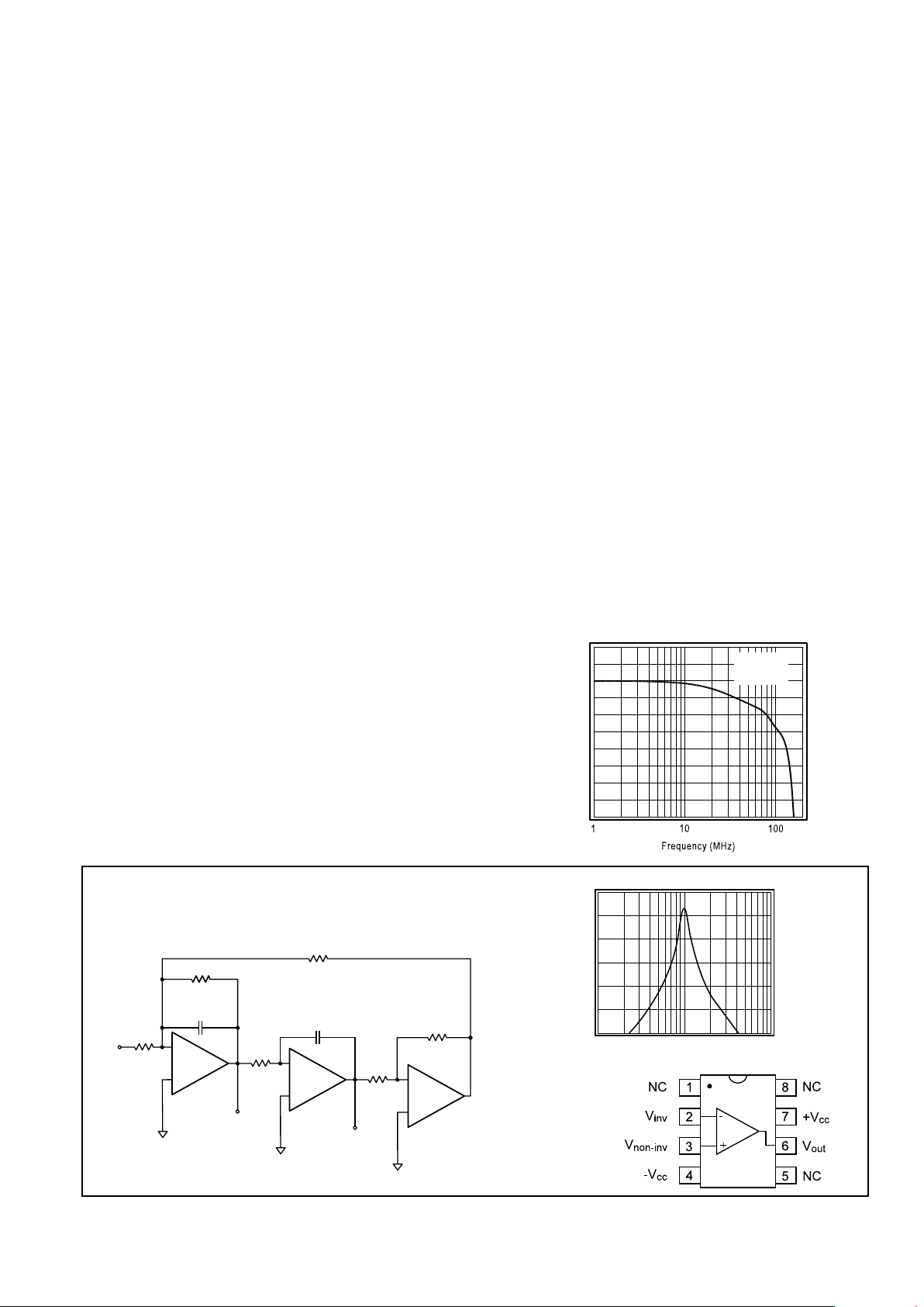
Frequency Response (Av = +2V/V)
V
out
= 0.5Vpp
V
cc
= ±15V
R
L
= 1kΩ
Magnitude (1dB/div)
C
120pF
Bandpass
Output
V
in
R
1
6631Ω
R
3
1326Ω
-
+
CLC436
R
4
3315Ω
-
+
CLC436
R
2
1326Ω
C
120pF
Low-pass
Output
-
+
CLC436
R
500Ω
R
500Ω
Typical Application
State-Variable Filter (1MHz, Q = 5, G = 2)
Pinout
DIP & SOIC
Bandpass Output
Magnitude (dB)
Frequency (MHz)
10
5
-20
0.1
1
10
0
-5
-10
-15
Comlinear CLC436
200MHz, ±15V, Low-Power Voltage Feedback Op Amp
August 1996
Comlinear CLC436
200MHz, ±15V, Low-Power Voltage Feedback Op Amp
N
© 1996 National Semiconductor Corporation http://www.national.com
Printed in the U.S.A.

PARAMETERS CONDITIONS V
cc
TYP MIN/MAX RATINGS UNITS NOTES
CLC436AJ 25° 25° 0° to +70° -40° to +85°
FREQUENCY DOMAIN RESPONSE
-3dB bandwidth V
out
< 0.5V
pp
(AJP) ±15, ±5 96,55 50 50 50 MHz B
V
out
< 0.5V
pp
(AJE) ±15, ±5 96,55 50 60 40 MHz B
V
out
< 10V
pp
25 21 20 16 MHz
-3dB bandwidth A
V
= +1 V
out
< 0.5Vpp, Rf = 0 ±15, ±5 200,150 MHz
gain flatness V
out
< 0.5V
pp
rolloff DC to 20MHz 0.6 1.2 1.2 1.2 dB B
peaking DC to 10MHz 0 0.03 0.03 0.03 dB B
linear phase deviation DC to 10MHz 0.5 deg
differential gain 4.43MHz, R
L
=150Ω 0.2 %
differential phase 4.43MHz, R
L
=150Ω 1.2 deg
gain bandwidth product V
out
< 2.0V
pp
±15, ±5 200,100 MHz
TIME DOMAIN RESPONSE
rise and fall time 2V step, t
r
(in) = 5ns 11 13 14 18 ns
5V step, t
r
(in) = 5ns 13 16 18 20 ns
settling time to 0.05% 2V step, t
r
(in) = 5ns ±15, ±5 36,48 42 65 85 ns
overshoot 2V step, t
r
(in) = 5ns 0.5 1 2 2 %
slew rate 5V step, t
r
(in) = 5ns ±15, ±5 2400,850 2000 1900 1600 V/µs
DISTORTION AND NOISE RESPONSE
2
nd
harmonic distortion 1V
pp,
1MHz -72 -65 -62 -62 dBc
3
rd
harmonic distortion 1V
pp,
1MHz -70 -62 -60 -60 dBc
2
nd
harmonic distortion 1V
pp,
5MHz -65 -56 -56 -53 dBc B
3
rd
harmonic distortion 1V
pp,
5MHz -63 -54 -54 -54 dBc B
input voltage noise @1kHz 11 12.6 13.5 14.1 nV/√Hz
current noise @1kHz 0.8 1.5 1.9 2.3 pA/√Hz
STATIC DC PERFORMANCE
input offset voltage ±15, ±5 1.5,1.5 5 5 5 mV A
average drift 6 – 40 70 µV/˚C
input bias current ±15, ±5 1,1.2 3 3 4 µAA
average drift 4 – 50 70 nA/˚C
input offset current ±15, ±5 0.1,0.1 1 1 3 µAA
power supply rejection ratio DC 95 75 75 75 dB B
common-mode rejection ratio DC 110 75 73 70 dB
supply current R
L
= ∞ 2.3 4 4 4 mA A
open loop gain ±15, ±5 85,80 dB
MISCELLANEOUS PERFORMANCE
input resistance common-mode 40 20 15 10 MΩ
input capacitance common-mode 2 3 3 5 pF
input resistance differential-mode 4.9 4.0 3.0 2.5 MΩ
input voltage range common-mode ±15 ±12 ±11 ±10.5 ±10 V
input voltage range common-mode ±5 ±3 V
output voltage range R
L
= 100Ω ±15 +11.6/-10.5 +8.5/-8.5 +8.5/-8.5 +8.5/-8.5 V
R
L
= ∞ ± 15 +13/-12.2 +12/-12 +12/-12 +12/-12 V
output voltage range R
L
= 100Ω ±5 ±2.8 V
R
L
= ∞ ±5 ±3.4 V
output resistance, closed loop 0.01 0.05 0.07 0.1 Ω
output current sourcing ±15, ±5 120,90 100 95 90 mA
output current sinking ±15, ±5 80,40 75 70 65 mA
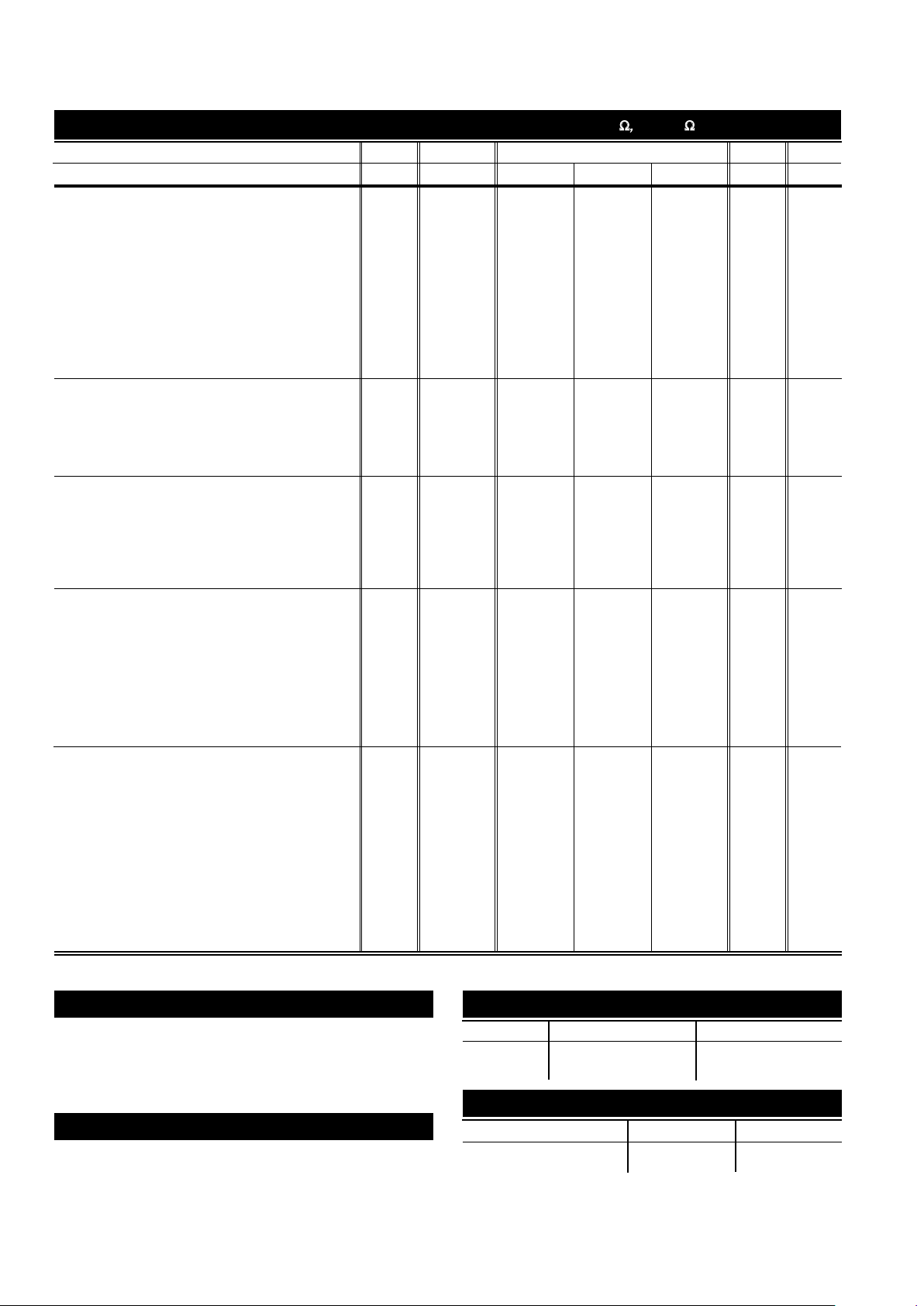
CLC436 Electrical Characteristics
(Vcc= ±15V, Av= +2, Rf= 499
W,
RL= 1kW; unless specified)
Absolute Maximum Ratings
supply voltage
±
18.0V
maximum junction temperature +150˚C
storage temperature range -65˚C to +150˚C
lead temperature (soldering 10 sec) +260˚C
Ordering Information
Model Temperature Range Description
CLC436AJP -40˚C to +85˚C 8-pin PDIP
CLC436AJE -40˚C to +85˚C 8-pin SOIC
Notes
A) J-level: spec is 100% tested at +25˚C, sample tested at +85˚C.
B)J-level: spec is sample tested at +25˚C.
Package Thermal Resistance
Package θ
JC
θ
JA
Plastic (AJP) 90°C/W 105°C/W
Surface Mount (AJE) 120°C/W 140°C/W
http://www.national.com 2
Min/max ratings are based on product characterization and simulation. Individual parameters are tested as noted. Outgoing quality levels are
determined from tested parameters.
 Loading...