

Page 1

Nokia Customer Care
RH-21 Series Transceivers
System Module
Issue 2 07/2004 2004 Nokia Corporation. Page 1
Company Confidential
Page 2

RH-21 Company Confidential
System Module Nokia Customer Care
Page 2 2004 Nokia Corporation. Issue 2 07/2004
Page 3

Company Confidential RH-21
Nokia Customer Care System Module
Contents
Page No
Transceiver RH-21......................................................................................................... 5
Introduction ..................................................................................................................5
Operational Modes .......................................................................................................6
Engine Module .............................................................................................................6
Environmental Specifications ................................................................................... 6
Temperature Conditions............................................................................................ 6
Baseband Module ........................................................................................................7
UEM ............................................................................................................................7
UEM introduction ..................................................................................................... 7
Regulators.................................................................................................................. 7
RF Interface............................................................................................................... 9
Charging Control....................................................................................................... 9
Digital Interface......................................................................................................... 9
Audio Codec.............................................................................................................. 9
UI Drivers................................................................................................................ 10
AD Converters......................................................................................................... 10
UPP8M .................................................................................................................... 10
Blocks...................................................................................................................... 10
Flash Memory ............................................................................................................10
Introduction ............................................................................................................. 10
User Interface Hardware .............................................................................................. 11
LCD ...........................................................................................................................11
Introduction ............................................................................................................. 11
Interface................................................................................................................... 11
Keyboard ....................................................................................................................11
Introduction ............................................................................................................. 11
Power Key ............................................................................................................... 11
Lights .........................................................................................................................11
Introduction ............................................................................................................. 11
Interfaces ................................................................................................................. 11
Technical Information ............................................................................................. 11
Vibra ..........................................................................................................................12
Introduction ............................................................................................................. 12
Interfaces ................................................................................................................. 12
Audio Hardware........................................................................................................... 12
Earpiece .....................................................................................................................12
Introduction ............................................................................................................. 12
Microphone ................................................................................................................12
Introduction ............................................................................................................. 12
MIDI Speaker ............................................................................................................12
Introduction ............................................................................................................. 12
Battery ........................................................................................................................13
Phone Battery .............................................................................................................13
Introduction ............................................................................................................. 13
Interface................................................................................................................... 13
Battery Connector ......................................................................................................14
Accessories Interface ................................................................................................... 15
Issue 2 07/2004 2004 Nokia Corporation. Page 3
Page 4

RH-21 Company Confidential
System Module Nokia Customer Care
System connector ......................................................................................................... 15
Introduction ............................................................................................................. 15
Interface................................................................................................................... 15
Technical Information ............................................................................................. 16
Charger IF ..................................................................................................................16
Introduction ............................................................................................................. 16
Interface................................................................................................................... 16
Test Interfaces .............................................................................................................. 17
Production Test Pattern ..............................................................................................17
Other Test Points .......................................................................................................17
EMC ............................................................................................................................. 17
General .......................................................................................................................17
BB Component and Control IO Line Protection .......................................................17
Keyboard lines......................................................................................................... 17
PWB ........................................................................................................................ 17
LCD......................................................................................................................... 18
Microphone ............................................................................................................. 18
EAR Lines/MIDI..................................................................................................... 18
System Connector Lines.......................................................................................... 19
Battery Connector Lines.......................................................................................... 19
M-bus F-bus ............................................................................................................ 19
Tranceiver Interfaces .................................................................................................19
BB - RF Interface Connections ..................................................................................19
BB Internal Connections ............................................................................................23
UEM Block Signal Description............................................................................... 23
UPP Block signals .....................................................................................................28
MEMORY Block Interfaces ......................................................................................31
...................................................................................................................................33
Audio Interfaces ...................................................................................................... 33
Baseband External Connections.............................................................................. 36
Test Pattern for Production Tests ............................................................................ 37
General Information About Testing ...........................................................................37
Phone operating modes ........................................................................................... 37
RF Module ................................................................................................................... 38
Requirements .............................................................................................................38
Temperature Conditions.......................................................................................... 38
Main Technical Characteristics .................................................................................39
RF Frequency Plan .................................................................................................. 39
DC Characteristics .....................................................................................................40
Power Distribution Diagram ................................................................................... 40
Regulators................................................................................................................ 41
Receiver................................................................................................................... 41
AMPS/TDMA 800 MHz Front End........................................................................ 42
TDMA 1900 MHz Front End.................................................................................. 42
Frequency Synthesizers........................................................................................... 44
Transmitter .............................................................................................................. 45
Antenna ......................................................................................................................47
Page 4 2004 Nokia Corporation. Issue 2 07/2004
Page 5
Company Confidential RH-21
A
Nokia Customer Care System Module
Transceiver RH-21
Introduction
The RH-21 (Model 3520) transceiver is a single-band TDMA800 transceiver unit.
The transceiver consists of engine module (1cb) and assembly parts.
The transceiver has a full graphic display and the user interface is based on the Jack 3.2
UI with two soft keys.
An internal antenna is used, there is no connection to an external antenna.
The transceiver has a low leakage tolerant earpiece and an omnidirectional microphone,
providing excellent audio quality.
TRANSCEIVER
ANT
EXT
RF
LCD DRIVER
B & W
display
BACKLIGHT
BACKLIGHT
✉
12 3
4
7
*
RF
☎
5
6
9
8
0#
ENGINE
USER IN T E R F AC E
EARPIECE
AUDIO
(disc r)
BUZZER
VIBRA
MIC
Ext. Audio
ccessories
Ostrich
BB
JTAG
Prod.TEST I/F
BSI
BTemp
BATTERY
CHARGER
Figure 1: Interconnecting Diagram
Issue 2 07/2004 2004 Nokia Corporation. Page 5
Page 6

RH-21 Company Confidential
System Module Nokia Customer Care
Operational Modes
There are several different operational modes. Modes have different states controlled by
the cellular SW. Some examples are: Idle State (on ACCH), Camping (on DCCH), Scanning,
Conversation, No Service Power Save (NSPS) previously OOR = Out of Range.
In the power off mode, only the circuits needed for power up are supplied.
In the idle mode, circuits are powered down and only the sleep clock is running.
In the active mode, all the circuits are supplied with power although some parts might
be in idle state part of the time.
The charge mode is effective in parallel with all previous modes. The charge mode itself
consists of two different states (i.e., the fast charge and the maintenance mode).
The local mode is used for alignment and testing.
Engine Module
Environmental Specifications
Normal and extreme voltages
Voltage range:
• nominal battery voltage: 3.6 V
• maximum battery voltage: 5.2 V
• minimum battery voltage: 3.1 V
Temperature Conditions
Temperature range:
• ambient temperature: -30...+ 60 °C
• PWB temperature: -30...+85 °C
Page 6 2004 Nokia Corporation. Issue 2 07/2004
Page 7
Company Confidential RH-21
Nokia Customer Care System Module
Baseband Module
The core parts of 3560/3520 BB consists of two ASICs—UEM and UPP—and flash memory.
The following sections describe these parts.
PA Supply
RF Supplies
RF RX/TX
EAR
MIC
LM4890
VIBRA
M
Battery
UEM
XEAR
DCT4 Janette connector
External Audio
Charger connection
Baseband
DLIGHT
KLIGHT
SLEEPCLK
32kHz
CBUS/
DBUS
BB
Supplies
MBus/FBus
MEMADDA
FLASH
Safari
RFBUS
UI
19.44MHz
UPP
UEM
UEM introduction
The UEM is the Universal Energy Management IC for DCT4 digital handportable phones.
In addition to energy management, it performs all the baseband mixed-signal functions.
Most UEM pins have 2kV ESD protection and those signals which are considered to be
exposed more easily to ESD have 8kV protection inside UEM. Such signals are all audio
signals, headset signals, BSI, Btemp, Fbus, and Mbus signals.
Regulators
The UEM has six regulators for BB power supplies and seven regulators for RF power supplies. The VR1 regulator has two outputs (VR1a and VR1b). In addition, there are two
current generators (IPA1 and IPA2) for biasing purposes.
A bypass capacitor (1uF) is required for each regulator output to ensure stability.
Figure 2: System Block Diagram (simple)
Issue 2 07/2004 2004 Nokia Corporation. Page 7
Page 8
RH-21 Company Confidential
System Module Nokia Customer Care
Reference voltages for regulators require external 1uF capacitors. Vref25RF is reference
voltage for VR2 regulator, Vref25BB is reference voltage for VANA, VFLASH1, VFLASH2,
VR1 regulators, Vref278 is reference voltage for VR3, VR4, VR5, VR6, VR7 regulators,
VrefRF01 is reference voltage for VIO, VCORE, VSIM regulators, and for RF.
BB RF Current
VANA: 2.78Vtyp 80mAmax VR1a:4.75V 10mAmax
IPA1: 0-5mA
VR1b:4.75V
Vflash1: 2.78Vtyp 70mAmax IPA2: 0-5mA
Vflash2: 2.78Vtyp
VR2:2.78V 100mAmax
40mAmax
VSim: 1.8/3.0V 25mAmax VR3:2.78V 20mA
VIO: 1.8Vtyp
VR4: 2.78V 50mAmax
150mAmax
Vcore: 1.0-1.8V
VR5: 2.78V 50mAmax
200mAmax
VR6: 2.78V 50mAmax
VR7: 2.78V 45mAmax
VANA regulator supplies internal and external analog circuitry of BB. It is disabled in
sleep mode.
Vflash1 regulator supplies LCD, IR-module and digital parts of UEM and Safari asic. It is
enabled during startup and goes to low Iq-mode in sleep mode.
Vflash2 regulator is not used.
VIO regulator supplies both external and internal logic circuitries. It's used by LCD, flash,
and UPP. Regulator goes in to low Iq-mode in sleep mode.
VCORE regulator supplies DSP and Core part of UPP. Voltage is programmable and the
start-up default is 1.5V. Regulator goes to low Iq-mode in sleep mode.
VSIM regulator is not used.
VR1 regulator uses two LDOs and a charge pump. Charge pump requires one external 1uF
capacitor in Vpump pin and 220nF flying capacitor between pins CCP and CCN. VR1 regulator is used by Safari RF ASIC.
VR2 regulator is used to supply external RF parts, lower band up converter, TX power
detector module, and Safari. In light load situations, VR2 regulator can be set to low
Iq-mode.
Page 8 2004 Nokia Corporation. Issue 2 07/2004
Page 9

Company Confidential RH-21
Nokia Customer Care System Module
VR3 regulator supplies VCTCXO and Safari in RF. It's always enabled when UEM is active.
When UEM is in sleep mode, VR3 is disabled.
VR4 regulator supplies RF parts having low noise requirements. In light load situations,
VR4 regulator can be set to low Iq-mode.
VR5 regulator supplies lower band PA. In light load situations, VR5 regulator can be set
to low Iq-mode.
VR6 regulator supplies higher band PA and TX amplifier. In light load situations, VR6 regulator can be set to low Iq-mode.
VR7 regulator supplies VCO and Safari. In light load situations, the VR7 regulator can be
set to low Iq-mode.
IPA1 and IPA2 are programmable current generators. 27kW/1%/100ppm external resistor
is used to improve the accuracy of output current. IPA1 is used by lower band PA and
IPA2 is used by higher band PA.
RF Interface
The interface between the baseband and the RF section also is handled by UEM. It provides A/D and D/A conversion of the in-phase and quadrature receive and transmit signal
paths and also A/D and D/A conversions of received and transmitted audio signals to and
from the UI section. The UEM supplies the analog AFC signal to RF section according to
the UPP DSP digital control. It also converts PA & VCTCXO temperature into real data for
the DSP.
Charging Control
The CHACON block of UEM asics controls charging. Needed functions for charging controls are pwm-controlled battery charging switch, charger-monitoring circuitry, and battery voltage monitoring circuitry. In addition, external components are needed for EMC
protection of the charger input to the baseband module. The DCT4 baseband is designed
to support both DCT3 and DCT4 chargers from an electrical point of view.
Digital Interface
Data transmission between the UEM and the UPP is implemented using two serial connections, DBUS (programmable clock) for DSP and CBUS (1.0MHz GSM and 1.08MHz
TDMA) for MCU. UEM is a dual voltage circuit, the digital parts are running from 1.8V
and the analog parts are running from 2.78V. Vbat (3,6V) voltage regulator inputs also
are used.
Audio Codec
The baseband supports two external microphone inputs and one external earphone output. The inputs can be taken from an internal microphone, from a headset microphone,
or from an external microphone signal source through headset connector. The output for
the internal earpiece is a dual-ended type output, and the differential output is capable
of driving 4Vpp to the earpiece with a 60 dB minimum signal to total distortion ratio.
Input and output signal source selection and gain control is performed inside the UEM
Issue 2 07/2004 2004 Nokia Corporation. Page 9
Page 10

RH-21 Company Confidential
System Module Nokia Customer Care
Asic according to control messages from the UPP. The buzzer and an external vibra alert
control signals are generated by the UEM with separate PWM outputs.
UI Drivers
There are discrete drivers for the MIDI speaker and keyboard LEDs. The drivers for vibra
and display are inside UEM.
AD Converters
There is an 11-channel analog-to-digital converter in UEM. The AD converters are calibrated in the production line.
UPP8M
RH-21 uses UPP8M ASIC. The RAM size is 8M. The UPP ASIC is designed to operate in a
DCT4 engine. The UPP processor architecture consists of both DSP and MCU processors.
Blocks
UPP is internally partitioned into two main parts:
The Processor and Memory System (i.e., Processor cores, Mega-cells, internal memories, peripherals, and external memory interface). This is known as the Brain.
The Brain consists of the blocks: the DSP Subsystem (DSPSS), the MCU Subsystem
(MCUSS), the emulation control (EMUCtl), the program/data RAM (PDRAM) and the
Brain Peripherals–subsystem (BrainPer).
The NMP custom cellular logic functions. This is known as the Body.
The Body contains all interfaces and functions needed for interfacing other DCT4 baseband and RF parts. Body consists of following sub-blocks: MFI, SCU, CTSI, RxModem,
AccIF, UIF, Coder, GPRSCip, BodyIF, SIMIF, PUP, and CDMA (Corona).
Flash Memory
Introduction
The RH-21 tranceivers use a 64-Mbit flash as its external memory. The VIO regulator is
used as a power supply for normal in-system operation. An accelerated program/erase
operation can be obtained by supplying Vpp of 12 volt to the flash device.
The device has two read modes: asynchronous and burst. The Burst read mode is utilized
in RH-21, except for the start-up, when the asynchronous read mode is used for a short
time.
In order to reduce the power consumpition on the bus, a Power Save function is introduced. This reduces the amount of switching on the external bus.
Page 10 2004 Nokia Corporation. Issue 2 07/2004
Page 11

Company Confidential RH-21
Nokia Customer Care System Module
User Interface Hardware
LCD
Introduction
RH-21 uses a color GD51 96 x 65 full dot-matrix graphical display. The LCD module
includes LCD glass, LCD COG-driver, spring connector, and metal frame. The LCD module
is included with the lightguide assembly module.
Interface
SW and the control signals are from the UPP asic. The VIO and Vflash1 regulators supply
the LCD with power. The LCD has an internal voltage booster and a booster capacitor is
required between Vout and GND.
Pin 3 (Vss) is the LCD driver's ground. LCD is controlled by UI SW and control signals.
Booster capacitor (C302 1 uF) is connected between booster pin (Vout) and ground. The
capacitor stores boosting voltage.
Keyboard
Introduction
The RH-21 keyboard follows the Jack III style.
PWR key is located on top of phone.
Power Key
All keyboard signals come from UPP asic, except pwr key signal, which is connected
directly to UEM. Pressing of pwr key is detected so that switch of pwr key connects
PWONX is of UEM to GND and creates an interrupt.
Lights
Introduction
RH-21 has LEDs for lighting purposes: two LEDs for keyboard and two LEDs for display.
LED type is TBSF (white).
Interfaces
Both the display and keyboard lights are controlled through a shared LED driver with a
constant current charge-pump circuit. The driver circuit is controlled by the Dlight signal
from UEM. With appropriate SW, the driver can be PWM controlled for dimming purpose.
Technical Information
LED locates in hole and terminals are soldered on the component side of the module
PWB. The LEDs have a white plastic body around the diode, and this directs the emitted
light better to the UI-side.
Issue 2 07/2004 2004 Nokia Corporation. Page 11
Page 12

RH-21 Company Confidential
System Module Nokia Customer Care
The current for the LCD lights is limited by the resistor between the ISET pin of the LED
driver and ground. For the keyboard lights, there are resistors in parallel.
Vibra
Introduction
The vibra is located on D-cover and is connected by spring connectors on PWB. It is
located in the left bottom side of the engine.
Interfaces
The vibra is controlled by the PWM signal VIBRA from the UEM. With this signal, it is
possible to control both the frequency and pulse width of signal. Pulse width is used to
control current when the battery voltage changes. Frequency control makes it possible to
search for an optimum frequency to provide silent and efficient vibrating.
Audio Hardware
Earpiece
Introduction
The 13 mm speaker capsule that is used in DCT3 products is also used in RH-21.
The speaker is dynamic. It is very sensitive and capable of producing relatively high sound
pressure at low frequencies.
Microphone
Introduction
The microphone is an electret microphone with an omnidirectional polar pattern. It consists of an electrically polarized membrane and a metal electrode which forms a capacitor. Air pressure changes (i.e., sound) move the membrane, which cause voltage changes
across the capacitor. Becauce the capacitance is typically 2 pF, a FET buffer is needed
inside the microphone capsule for the signal generated by the capacitor. Because of the
FET, the microphone requires a bias voltage.
MIDI Speaker
Introduction
The speaker being used to generate MIDI ring tones is a 13mm SALT speaker. The SALT
speaker is mounted in the D-cover, kept in position by a double adhesive gasket that is
mounted on the front of SALT. The useful frequency range is approximately 340 Hz to
8KHz.
Page 12 2004 Nokia Corporation. Issue 2 07/2004
Page 13
Company Confidential RH-21
Nokia Customer Care System Module
Battery
Phone Battery
Introduction
The battery for the 3560/3520 is the BLC-2 (Li-Ion 1000 mAh).
Interface
The battery block contains BTEMP and BSI resistors for temperature measurement and
battery identification. The BSI fixed resistor value indicates the chemistry and default
capacity of a battery. BTEMP-resistor measures the battery temperature. Temperature
and capacity information is needed for charge control. These resistors are connected to
BSI and BTEMP pins of the battery connector. Phone has pull-up resistors (R202) for
these lines so that they can be read by A/D inputs in the phone (see figure below). There
also are spark gaps in the BSI and BTEMP lines to prevent ESD.
Figure 3: Battery Connections.
Batteries have a specific red line which indicates if the battery has been subjected to
excess humidity. The batteries are delivered in a "protection" mode, which gives longer
storage time. The voltage seen in the outer terminals is zero (or floating), and the battery
is activated by connecting the charger. Battery has internal protection for overvoltage
and overcurrent.
1 (+)2(BSI)3(BTEMP)4(GND)
Figure 4: BLC-2 Battery contacts.
Issue 2 07/2004 2004 Nokia Corporation. Page 13
Page 14
RH-21 Company Confidential
System Module Nokia Customer Care
Battery Connector
RH-21 uses string type connector. This makes it easier to assemble the phone in production; and connection between battery and PWB is more reliable.
Signal
#
name
Connected
from - to
Batt I/O
Signal properties
A/D--levels--freq./timing
Description /
Notes
1 VBAT VBAT I/O Vbat 3.1-5.2V Battery volt-
age
2 BSI UEM Out Ana Battery size
indicator
3 BTEMP UEM Out Ana 40mA/
switch
400mA
Battery temperature indicator
4 GND Gnd Ground
Page 14 2004 Nokia Corporation. Issue 2 07/2004
Page 15
Company Confidential RH-21
Nokia Customer Care System Module
Accessories Interface
System connector
Introduction
RH-21 uses DCT4-accessories via DCT4 system connector.
Interface
The interface is supported by DCT4-compatible, fully differential 4-wire (XMICN, XMICP,
XEARN, and XEARP) accessories.
GND
VIN
PWMO
XMICP
XMICN
HF
HEADI HFC
MICN MIC
Figure 5: System Connector.
An accessory is detected by the HeadInt- line, which is connected to the XMIC. When
accessory is connected, it generates headint- interruption (UEMINT) to MCU. After that,
hookInt line is used to determine which accessory is connected. This is done by the voltage divider, which consists of phone's internal pull-up and accessory specific pull-down.
Voltage generated by this divider is then read by the ad- converter of UEM. The HookIntinterrupt is generated by the button in the headset or by the accessory external audio
input.
Issue 2 07/2004 2004 Nokia Corporation. Page 15
Page 16

RH-21 Company Confidential
System Module Nokia Customer Care
2.7V
Hookint
/MBUS
Headint Headint
HFCM
EAD
MIC1&3 Bias
MIC1P
MIC1N
HF
3...25k
UEM
Technical Information
ESD protection is made by spark gaps, buried capacitor and inside UEM, which is pro-
tected ±8 kV. RF and BB noise is prevented by inductors.
2.1V
33N
0.8V
Figure 6: Accessory Detection / External Audio.
2k2
1.8V
0.3V
Charger IF
Introduction
The charger connection is implemented through the bottom connector. DCT-4 bottom
connector supports charging with both plug chargers and desktop stand chargers.
There are three signals for charging. Charger gnd pin is used for both desktop and for
plug chargers as well as charger voltage. PWM control line, which is needed for 3-wire
chargers, is connected directly to gnd in module PWB so the engine doesn't provide any
PWM control to chargers. Charging controlling is done inside UEM by switching UEM
internal charger switch on/off.
Interface
The fuse F100 protects the phone from currents that are too high (for example, when
broken or pirate chargers are used). L100 protects engine from RF noise, which may
occur in charging cable. V100 also protects the UEM asic from reverse polarity charging
voltage and from excessive charging voltage. C105 is also used for ESD and EMC protection. Spark gaps are used for ESD protection right after the charger plug.
Page 16 2004 Nokia Corporation. Issue 2 07/2004
Page 17

Company Confidential RH-21
X
Nokia Customer Care System Module
Test Interfaces
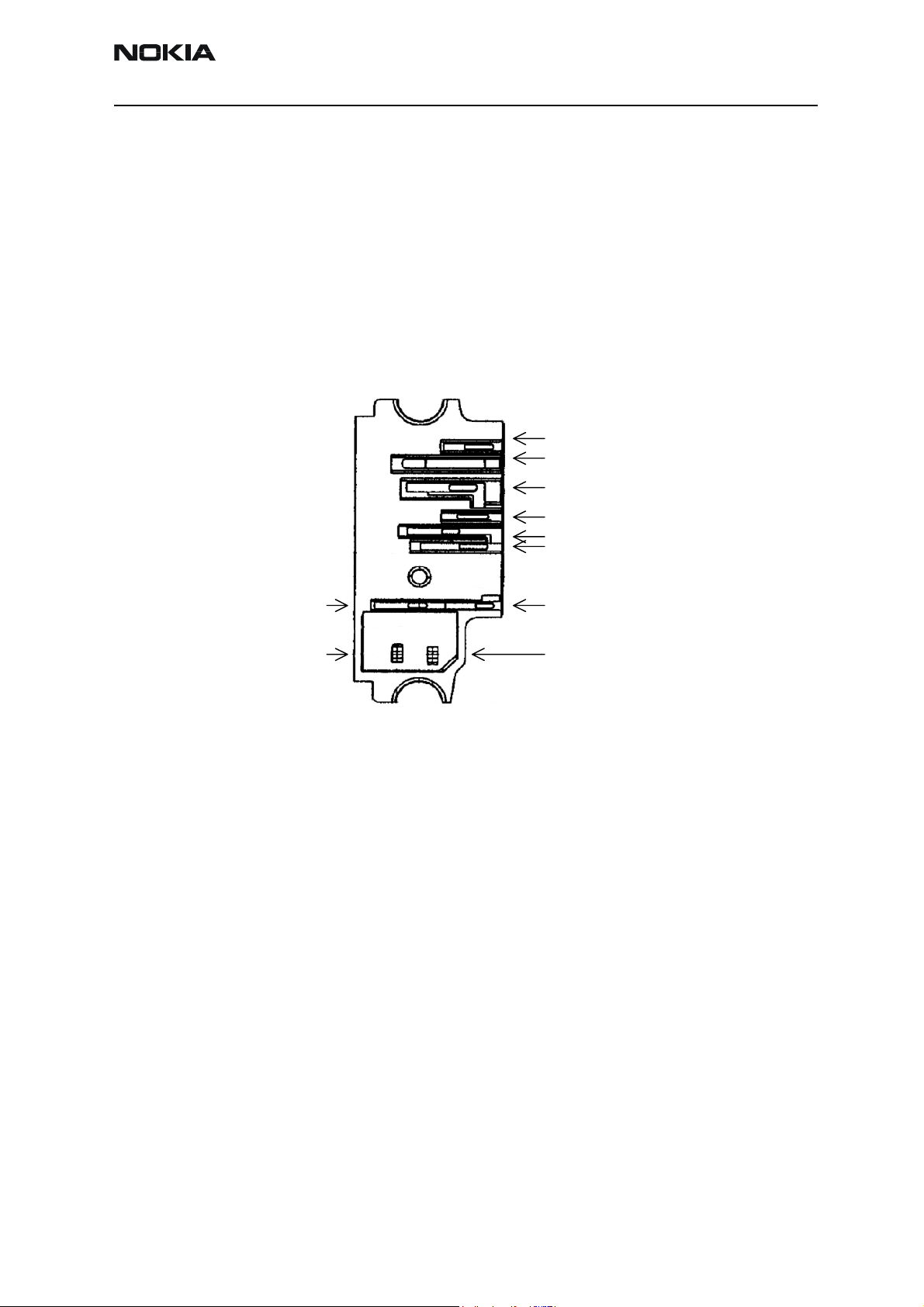
Production Test Pattern
Interface for RH-21 production testing is 5-pin pad layout in BB area (see figure below).
Production tester connects to these pads by using spring connectors. Interface includes
MBUS, FBUSRX, FBUSTX, VPP and GND signals. Same pads also are used for AS test
equipments such as module jig and service cable.
Other Test Points
Because BB asics and flash memory are CSP components, the access to BB signals is very
poor. This makes measuring of most of the BB signals impossible. In order to debug BB at
least on some level, the most important signals can be accessed from 0.6 mm test points.
EMC
General
There are many ways to protect the phone from EMC. One form of protecting BB against
EMC is a shield to cover main components of BB — components such as UEM, UPP and
Flash. UEM has internal protection against ±8kV ESD pulse. BB shield has a removable lid
so repairing of BB is possible. Shield also improves thermal dissipation by spreading the
heat more widely.
7.
MBUS
3.
FBUS_RX
8.
GND
2.
FBUS_T
6.
VPP
Figure 7: Top View of Production Test Pattern
BB Component and Control IO Line Protection
Keyboard lines
The keyboard PWB layout consists of a grounded outer ring and either a "trefoil pattern"
grid (matrix) or an inner pad. This construction makes the keys immune for ESD, as the
keydome will have a low ohmic contact with the PWB ground.
The keyboard is controlled entirely by the UPP. The rows and columns are ESD protected
by diodes and spark gaps.
PWB
The PWB has been designed to shield all lines susceptible for radiation. Sensitive PWB
Issue 2 07/2004 2004 Nokia Corporation. Page 17
Page 18

RH-21 Company Confidential
System Module Nokia Customer Care
tracks have been drawn with respect to shielding by having ground plane over tracks,
and ground close to the tracks at the same layer.
All edges are grounded from both sides of PWB and solder mask is opened from these
areas. Target is that any ESD pulse faces ground area when entering the phone; for
example, between mechanics covers. All holes in PWB are grounded and plated through
holes.
LCD
ESD protection for LCD is implemented by connecting metal frame of LCD in to gnd. Connection is only on one side, at the top of the LCD.
Microphone
Microphone signals are input lines and therefore very sensitive to radiated fields. Immunity for radiated fields is done to obtain a low impedance path and with respect to a
common noise point of view in the signal path. This is applied for both internal and
external microphone lines. Microphone is an unsymmetrical circuit, which makes it well
protected against EMC.
EAR Lines/MIDI
Internal EAR lines are EMC/ESD protected by radiated fields from the earpiece by the low
impedance signal path in the PWB.
The same PWB outline has been implemented for the SALT speaker. Low ohm coils are
used in series with the speaker for immunity against incoming fields from the speaker.
Page 18 2004 Nokia Corporation. Issue 2 07/2004
Page 19

Company Confidential RH-21
Nokia Customer Care System Module
System Connector Lines
System Connector signals that have EMC protection
Protection
type
ferrite bead
(600 /
199MHz)
ferrite bead
(420 /
100MHz)
spark gaps XXXXXX
PWB capacitors
RC-circuit XXXXX
capacitor to
ground
HF and HFCM lines have spark gaps, and a ferrite bead RF filter (450 W/100 MHz).
Headint and Hookint have spark gaps as well as an RC-circuit.
VIN XMIXP XMICN XEARP XEARN HEAD-
INT
XXXX X
X
XXXXXX
XXXXX
MICP
Charger + is protected with a ferrite bead (42 W/100 MHz) and capacitor to ground (1 n).
Charger - is protected with a ferrite bead (42 W/100 MHz).
Battery Connector Lines
BSI and BTEMP lines are protected with spark gaps and RC-circuit where resistors are
size 0402.
M-bus F-bus
The FBus and MBus lines are protected with spark gaps and resistors.
Tranceiver Interfaces
BB - RF Interface Connections
All the signal descriptions and properties in the following tables are valid only for active
Issue 2 07/2004 2004 Nokia Corporation. Page 19
Page 20

RH-21 Company Confidential
System Module Nokia Customer Care
signals.
Signal
RIP
name
RFICCNTRL(2:0) RF IC Control Bus from UPP to RF IC (SAFARI)
0 RFBUSCLK UPP RFIC In Dig 0/1.8V
1 RFBUSDA UPP/
2 RFBUSEN1X UPP RFIC In Dig RFIC Chip Set X
PUL (2:0) Power Up Reset from UEM to RF IC (SAFARI)
0 PURX UEM RFIC Out Dig 0/1.8V 10us Power Up Reset for RFIC
GEN (28.0) General I/= Bus connected to RF, see also separate collective
5 TXP1 RFIC,
Connected
from - to
RFIC
RFIC
Loband
mixer
UPP
UPP Out Dig 0/1.8V 10 us Low Band Tx enabled
BB I/O
I/O Dig Bi-directional RF Control
GEN(28.0) table
Control lines from UPP GENIOs to RF
Signal Properties
A/D Levels-Freq./
Timing resolution
9.72
(0: <0.4V
1: >1.4V
MHz
Description / Notes
RF Control serial bus bit
clock
serial bus data.
SLCLK & SLEEPX not used in
RF
6 TXP2 RFIC UPP Out Dig 0/1.8V High band Tx enabled
RFCLK (not BUS -> no rip #) System Clock from RF to BB, original source VCTCXO, buffered (and
frequency shifted, WAM only) in RF IC (SAFARI)
RFCLK VCTCX
O ->
RFIC
RFClk
GND
SLOWAD(6:0) Slow Speed ADC Lines from RF block
5PDMID RF
RF UPP In Ana 0 System Clock slicer Ref
Power
detection
module
UPP In ANA 800mVpp
typ (FET
probed)
Bias DC
blocked at
UPP input
UEM In Ana 0/2.7V dig 0/VR2 Power detection module
19.44
MHz
System Clk from RF to BB
GND, not separated from
pwb GND layer
identification to slow ADC
(ch 5, previous VCTCXO
Temp) signal to UEM
Page 20 2004 Nokia Corporation. Issue 2 07/2004
Page 21

Company Confidential RH-21
Nokia Customer Care System Module
Signal
RIP
name
6PATEMP RF
RFCONV(9:0) RF-BB differential Analog Signals: Tx I&Q, Rx I&Q and reference
0 RXIP RFIC UEM In Ana 1.4Vpp
1RXIN
2 RXQP Diff. positive/negative quad-
3RXQN
4 TXIP UEM RFIC Out Ana 2.2Vpp
5TXIN
6 TXQP Diff. positive/negative quad-
7TXQN
Connected
from - to
UEM In Ana 0.1-2.7V - Tx PA Temperature to UEM,
Power
detection
module
BB I/O
voltages
Signal Properties
A/D Levels-Freq./
Timing resolution
max. diff.
0.5Vpp typ
bias 1.30V
max. diff.
0.6Vpp typ
bias 1.30V
Description / Notes
NTC in Power Detection
Module
Differential positive/negative in-phase Rx Signal
rature phase Rx Signal
Differential positive/negative in-phase Tx Signal
rature phase Tx Signal
9 VREFRFO1 UEM RFIC Out Vref 1.35 V RF IC Reference voltage
from UEM
RFAUXCON(2:9) RF-BB Analog Control Signals to/from UEM
1 TXPWRDET TXP
Det.
2 AFC UEM VCTCXOOut Ana 0.1-2.4V Automatic Frequency Con-
VRF Globals instead of Bus Regulated RF Supply Voltages from UEM to RF. Current values are of
VR1 A UEM RFIC Out Vreg 4.75 V
VR1 B UEM RFIC Out Vreg 4.75 V
VR2 UEM RFDis
VR3 UEM VCTCXOOut Vreg 2.78 V
UEM In Ana 0.1-2.4V 50 us Tx PWR Detector Signal to
UEM
trol for VCTCXO
the regulator specifications, not the measured values of RF
cr./
RFIC
+- 3%
+- 3%
Out Vreg 2.78 V
+- 3%
+- 3%
10mA
max.
10mA
max.
100
mA
max.
20mA
max.
UEM, charge pump + linear
regulator output. Supply for
UHF synth phase det...
UEM, charge pump + linear
regulator output. Supply for
Tx VHF VCO.
UEM linear regulator. Supply
voltage for Tx IQ filter and
IQ to Tx IF mixer.
UEM linear regulator. Power
supply to VCTCXO + RFCLK
Buffer in RF IC.
Issue 2 07/2004 2004 Nokia Corporation. Page 21
Page 22

RH-21 Company Confidential
System Module Nokia Customer Care
Signal
RIP
name
VR4 UEM RFIC Out Vreg 2.78 V
VR5 UEM RFIC Out Vreg 2.78 V
VR6 UEM RFIC Out Vreg 2.78 V
VR7 UEM RFIC,
IPA1 UEM RF PA Out Iout 0-5 mA Settable Bias current for RF
IPA2 UEM RF PA Out Iout 0-5 mA Settable Bias current for RF
VFLASH1 UEM RFIC Out Iout 2.78V 12mA UEM linear regulator com-
Connected
from - to
UHF
VCO
BB I/O
Out Vreg 2.78 V
Signal Properties
A/D Levels-Freq./
Timing resolution
50mA
+- 3%
+- 3%
+- 3%
+- 3%
max.
50mA
max.
50mA
max.
45mA UEM linear regulator. Power
Description / Notes
UEM linear regulator. Power
supply for LNA/RFIC Rx
chain.
UEM linear regulator. Power
supply for RF low band PA
driver section.
UEM linear regulator. Power
supply for RF high band PA
driver section.
supply for RF Synthes.
PA L-Band
PA H-Band
mon for BB. RFIC digital
parts and F to BB digl. IF.
VBATT, Global
VBATTRF Batt
Conn
RFPA Out Vbatt 3...5V 0...1A
2A
peak
Raw Vbatt for RF PA
Page 22 2004 Nokia Corporation. Issue 2 07/2004
Page 23

Company Confidential RH-21
Nokia Customer Care System Module
BB Internal Connections
UEM Block Signal Description
Signal
RIP
name
RFCONVDA(5:0)* 1.8V digital interface between UPP and UEM. RF converter CLK. Rx and
0 RFCONVCLK UPP UEM In Dig 0/1.8V 4.86
1 RXID UEM UPP Out (PDM) RxI Data
2RXQD
3 TXID UPP UEM In (PDM) TxI Data
4TXQD
5 AUXDA UPP UEM In Auxiliary DAC Data
RFCONVCTRL(2:0)* 1.8V digital interface between UPP (DSP) and UEM. RF converter UEM
Connected
from - to
UEM I/O
Tx I&Q data (bit stream signals).
RF IF bidirectional serial Control Bus, “DBUS”.
Signal Properties
A/D Levels-Freq./
Timing resolution
MHz/
Digi
3.24
MHz /
Ana
Description / Notes
RF Converter Clock
(PDM) RxQ Data
(PDM) TxQ Data
0 DBUSCLK UPP UEM In Dig 0/1.8V 9.72MHz Clock for Fast Control to
UEM
1DBUSDA In/
Out
2 DBUSENX In Fast Control Data Load /
AUDUEMCTRL(3.0)* 1.8V digital interface between UPP (MCU) and UEM. Bidirectional Con-
trol Bus “CBUS”
0 UEMINT UEM UPP Out Dig 0/1.8V UEM Interrupt
1 CBUSCLK UPP UEM In 1.08MHz Clock for control/Audio
2CBUSDA In/
Out
3 CBUSENX In Control Data Load Signal
AUDIODATA(1:0)* 1.8V digital audio interface between UPP and UEM audio codec. PDM
data clocked by CBUSCLK
0 EARDATA UPP UEM In Dig 0/1.8V 1.08Mbit/sPDM Data for Downlink
1.08Mbit/sControl data
Fast Control Data to/from
UEM
Enable to UEM
Convertors in UEM
Audio, clocked by CBUSCLK
1 MICDATA UEM UPP Out PDM Data forUplink Audio,
clocked bu CBUSCLK
Issue 2 07/2004 2004 Nokia Corporation. Page 23
Page 24

RH-21 Company Confidential
System Module Nokia Customer Care
Signal
RIP
name
PUSL(2:0)* Power-Up & Sleep Control lines
0PURX UEMUPP
1 SLEEPX UPP UEM In Power Save Functions, 0 at
2 SLEEPCLK UEM UPP Out 32 KHz 32 KHz Sleep Clock
IACCDIF(5:0)* BB Internal 1.8V Digital Accessory Buses between UPP and 2.7V level
0IRTX
IRRX
1
2MBUSTX
MBUSRX
3
4FBUSTXI
FBUSRXI
5
Connected
from - to
RFIC
UPP
UEM
UPP
UEM
UPP
UEM
UEM
UPP
UEM
UPP
UEM
UPP
UEM I/O
Out Dig 0/1.8V Power Up Reset, 0 at reset
shifter UEM
OutInDig 0/1.8V 1.152
In
Out
In
Out
Signal Properties
A/D Levels-Freq./
Timing resolution
Mbit/s
max
Dig 0/1.8V 9k6 b/s
9k6 b/s
< 7 Mb/s
Dig 0/1.8 V <115kb/s
<1Mb/s
<115kb/s
<7Mb/s
Description / Notes
sleep
Infrared Transmit
Infrared Receive
MBUS Transmit
MBUS Receive / FDL Clk
FBUS Transmit / FDL Tx
FBUS Receive / FDL Rx
Signal
RIP
name
SLOWAD(6:0)* SLow Speed ADC Lines, UEM external
0BSI BAT-
1BTEMP
5PDMid RF
6PATEMP RF,
RFCONV(9:0)* RF - BB Analog Signals: Tx I&Q, Rx I&Q and ref
0 RXIP RFIC UEM In Ana 1.4Vpp max
1RXIN
2 RXQP Diff. positive/negative quad-
3RXQN
Connected
from - to
UEM In Ana 0-2.7V Battery Size Indicator/FDL
TERY
UEM In Ana 0-2.7V Power detection module
PDMo
d
PDMo
d NTC
UEM I/O
Signal Properties
A/D Levels-Freq./
Timing resolution
diff.
0.5Vpp typ
bias 1.30V
Description / Notes
init
Battery Temperature
identification to slow ADC
(ch, previous VCTCXO Temp)
signal to UEM.
Differential positive/negative in-phase Rx Signal
rature phase Rx Signal
Page 24 2004 Nokia Corporation. Issue 2 07/2004
Page 25

Company Confidential RH-21
Nokia Customer Care System Module
Signal
RIP
name
4 TXIP UEM RFIC Out Ana 2.2Vpp max
5TXIN
6 TXQP Differential positive/nega-
7TXQN
9 VREFRFO1 UEM RFIC Out Vref 1.35V RF IC Reference voltage
HP INTERNAL AUDIO
AUDIO(4:0) HP Internal analog ear & microphone IF between UEM and Mic/Ear circuitry
0 EARP UEM Ear-
1EARN
2 MIC1N Mic UEM In Ana 100mVpp
3MIC1P
4 MICB1 Mic UEM Out V bias 2.1V typ./
Connected
from - to
piece
UEM I/O
Out Ana 1.25V Audio Differential signal to HP
Signal Properties
A/D Levels-Freq./
Timing resolution
diff.
0.6VppTyp
Bias 1.30V
Audio Differential signal from HP
max diff.
DC Bias Bias voltage for internal
<600 uA
Description / Notes
Differential positive/negative in-phase Tx Signal
tive quadrature phase Tx
Signal
from UEM
internal Earpiece.
Load resistance 32 ohm.
internal MIC, 2mV nominal
MIC
EXTERNAL AUDIO INTERFACE
XAUDIO(9:0)* External Audio IF between UEM and X-audio circuitry
0 HEADINT SysCo
n/
HSet
1 HF UEM SysCo
2 HFCM Ana 0.8 Vdc
3 MICB2 UEM SysCo
4MIC2P
MIC2N
5
6 HOOKINT Sys
SysCo
n/
Headset
Con
UEM In Dig 0/2.7V Input for Headset Connector
Out Ana 1.0Vpp
n/
HSet
Out V bias 2.1V typ/
n/
HSet
UEM In Ana 200mVpp
UEM In Ana/
Dig
bias 0.8V
600 uA
max diff
0...2.7V DC HS Button interrupt, Exter-
Audio External Earpiece Audio Sig-
Audio Differential signal from
HeadInt Switch
nal
Reference output for DC
coupled external Earpiece
Bias voltage for external
MIC
external MIC
nal Audio Accessory Detect
(EAD)
CHARGER INTERFACE
CHARGER lines, no bus*
Issue 2 07/2004 2004 Nokia Corporation. Page 25
Page 26

RH-21 Company Confidential
System Module Nokia Customer Care
Signal
RIP
name
VCHARGIN ChargerUEM In Vchr < 16 V
GND GND GND from/to Charger con-
PWRONX * Power On Signal, see also the UI/keyboard
PWRONX UI UEM In Dig 0/Vbatt Power button
GND GND GND from/to Charger con-
RFAUXCONV(2:0) RF-BB auxiliary analog signals
0
1 TXPWRDET TXPow
2 AFC UEM VCTCXOOut Ana 0.1-2.4V 11bits AFC control voltage to
Connected
from - to
UEM In Ana 0.1-2.7V Tx PWR Detector Output to
. Det.
Mod.
UEM I/O
Signal Properties
A/D Levels-Freq./
Timing resolution
DC Vch from Charger Connec-
<1.2 V
Description / Notes
tor, max. 20 V
nector
nector
UEM
VCTCXO, default about 1.3V
IRIF, no bus no rips UEM 2.7V signals to IR Module
IRLEDC UEM IR Out Dig 0/2.7V 9k6 -
1Mbit/s
IRRXN IR UEM In Dig 0/2.7V 9k6 -
1Mbit/s
UIDRV lines, no bus UEM drivers: sinking outputs to Buzzer, Vibra, KLED, DLED
BUZZO UEM BuzzerOut Dig 350mA max.
/ Vbatt
VIBRA UEM Vibra Out Dig 135mA max
/ Vbatt
DLIGHT UEM UI Out Dig 100mA /
Vbatt
KLIGHT UEM UI Out Dig 100mA /
Vbatt
1-5 kHz,
PWM vol
64/128/
256/512
Hz
Switch/
100Hz
pwm
Switch/
100Hz
pwm
IR Tx signal to IR Module
IR Receiver signal from IR
Module
Open collector sink switch
output for Buzzer. Frequency controlled pitch,
PWM for volume.
Open collector sink switch/
Frequency/ pwm output for
buzzer
Open drain switch/pwm
output for display light
Open drain switch/pwm
output for key light
ACCDIF lines, no bus * Wired Digital Accessory Interface, only to test pattern
MBUS UEM Test
Pad 7
In/
Dig 0/2.7 V 9k6bit/s Mbus bidirectional asyn-
Out
chronous serial data bus/
FDL clock, 0-8MHz depends
on project
Page 26 2004 Nokia Corporation. Issue 2 07/2004
Page 27

Company Confidential RH-21
Nokia Customer Care System Module
Signal
RIP
name
FBUSTXO UEM Test
FBUSRXO Test
RTCBATT lines, no bus * Connector pads for Real Time Clock back up battery
VBACK UEM RTC-
GND Global GND 0
VBB, Globals instead of Bus* Regulated BB Supply Voltages
VANA UEM Out Vreg 2.78V
VFLASH1 UEM Out Vreg 2.78V
Connected
from - to
Pad 2
UEM In Dig 0/2.7 V 9k6-
Pad 3
BATT
UEM I/O
Out Dig 0/2.7 V 9k6-
In/
Vsup-
Out
ply/
Chrg
Signal Properties
A/D Levels-Freq./
Timing resolution
115kbit/s
115kbit/s
+2-3.3V For back up battery Li
80mA
+-3%
+-3%
max.
70mA
max
Description / Notes
Fbus asynchronous serial
data output / FDL data out
<1Mbit/s
Fbus asynchronous serial
data input/FDL in, 0-8Mbit/s
depends on project
6.8x1.4
2.3mAh@3.3V
Disable in sleep mode
1.5mA max. in sleep mode.
VFLASH1 is always enabled
after power on.
VFLASH2 UEM Out Vreg 2.78V
+-3%
VIO UEM Out Vreg 1.8V
+-4.5%
VCORE UEM Out Vreg 1.0-1.8V
+-5%
VBACK UEM In/
Vreg 3.0 V No external use, only for
Out
40mA
max.
150mA
max.
200mA
max.
VFLASH2 is disabled by
default
1.5mA max. in sleep mode.
VIO is always enabled after
power on.
200 uA max. in sleep mode
RTC battery charging/discharging.
Issue 2 07/2004 2004 Nokia Corporation. Page 27
Page 28

RH-21 Company Confidential
p
System Module Nokia Customer Care
UPP Block signals
RFCONVDA(5:0) See UEM / RFCONVDA(5:0)
RFCONVCTRL(2:0) See UEM / RFCONVCONTR(2:0)
AUDUEMCTRL(3:0) See UEM / AUDUEMCTRL(3:0)
AUDIODATA(1:0) See UEM / AUDIODATA(1:0)
ISIMIF(2:0) See UEM / ISIMIF(2:0)
PUSL(2:0) See UEM / PUSL(2:0)
IACCDIF(5:0) See UEM / IACCDIF(5:0)
RFCLK & GND See BB_RF IF Conn / RFCLK (not BUS …)
RFICCNTRL(2:0) See BB_RF IF Conn / RFICCNTRL(2:0)
GENIO(28:0)/rips 5 and 6 See BB_RF IF Conn / GENIO(28:0) also Sec 5.2.4
Ri
Signal
Name
#
DAMPS/
GSM1900
UPP Globals, no bus, no rip Power supplies and GND
VIO UPP UEM
VCORE UPP UEM
GND UPP VSSXXX 0 Global GND
Connected
from --- to
UPP
I/O
In Vreg
In Vreg
Signal Properties
A/D--Levels---Freq./
Timing resolution
1.8 V
+- 4.5 %
1.0-1.8 V
+- 5 %
20mA max. UPP I/O power supply
100mA
max.
Description / Notes
UPP logics and processors power supply,
settable to reach the speed for various clock
frequencies.
MEMADDA(23:0)* See Table 16. Memory Interface Signals / MEMADDA(23:0)*
MEMCONT(9:0) See Table 16. Memory Interface Signals / MEMCONT(8:0)
GENIO(28:0) See Table 16. Memory Interface Signals / GENIO(28:0)
Signal Properties
A/D Levels-Freq./
Timing resolution
Description / Notes
RIP
Signal
name
Connected
from - to
UPP
I/O
GENIO(28:0) General I/O Pins. Bolded lines are only valid for one product
0Switch con-
trol for
UPP Out Dig 0-1.8 V In/Pull
Up
Used to enable/disable
power to DLR-3 cable
SGND Vdd
1 Emu/Present UPP In Dig 0-1.8 V In/Pull UpR&D only
2 RTS UPP In Dig 0-1.8 V In / Pull UpUsed as request to send
input from DLR-3 cable
Page 28 2004 Nokia Corporation. Issue 2 07/2004
Page 29

Company Confidential RH-21
Nokia Customer Care System Module
Signal
RIP
name
3 Not Used UPP Out Dig 0-1.8 V In / Pull
4 LCDRstX UPP Dis-
5 TXP1 UPP RF Out Dig 0-1.8 V Out / 0 Tx Power Enable (low Band)
6 TXP2 UPP RF Out Dig 0-1.8 V Out / 0 Tx Power Enable (High
7 Not Used UPP Out Dig 0-1.8 V In / Pull
8 Not Used UPP Out Dig 0-1.8 V In / Pull
9 Not Used UPP Out Dig 0-1.8 V In / Pull
10 Smart Cover
Driver
Connected
from - to
play
UPP Smart
cover
driver
UPP
I/O
Out Dig 0-1.8 V Out / 0 Display reset
Out Dig 0-1.8 V In / Pull
Signal Properties
A/D Levels-Freq./
Timing resolution
Down
Down
Down
Down
Down
Description / Notes
Band)
Smart cover driver control
11 Not Used UPP Out Dig 0-1.8 V In / Pull
Up
12 Not Used UPP In/
13 Not Used UPP IR / RF Out Dig 0-1.8 V In / Pull UpFast IR
14 SHUTDOWN UPP MIDI
driver
15 Not Used UPP Out Dig 0-1.8 V In / Pull
16 Not Used UPP In Dig 0-1.8 V In / Pull
17 Not Used UPP In Dig 0-1.8 V In / Pull
18 Not Used UPP Out Dig 0-1.8 V In / Pull
19 Not Used UPP LPRF/RFIn/
20 Not Used UPP LPRF Out Dig 0-1.8 V Out / 0 LPRF Data Out
Dig 0-1.8 V In / Pull
Out
In Dig 0-1.8 V In / Pull
Dig 0-1.8 V In / Pull
Out
Down
Down
Down
Up
Up
Down
Down
MIDI driver shutdown
LPFR Data In / Accessory
Buffer Enable / PAGain
21 Not Used UPP LPRF Out Dig 0-1.8 V In / Pull UpLPRF Sync / Accessory Mute
22 Not Used UPP LPRF Out Dig 0-1.8 V In / Pull
Down
LPRF Interrupt/Accessory
Power Up
Issue 2 07/2004 2004 Nokia Corporation. Page 29
Page 30

RH-21 Company Confidential
System Module Nokia Customer Care
Signal
RIP
name
23 FLSWRPX UPP FLASH Out Dig 0-1.8 V Out / 1 Write Protect, 0-active
24 Not Used UPP Out Dig 0-1.8 V In / Pull
25 Not Used UPP In/
26 Not Used UPP Out Dig 0-1.8 V In / Pull
27 Not Used UPP In/
28 Not Used UPP Out Dig 0-1.8 V Out / 1
Connected
from - to
UPP
I/O
Out
Out
Signal Properties
A/D Levels-Freq./
Timing resolution
Up
Dig 0-1.8 V In / Pull
Up
Down
Dig 0-1.8 V In / Pull
Up
Description / Notes
when protected
Page 30 2004 Nokia Corporation. Issue 2 07/2004
Page 31

Company Confidential RH-21
Nokia Customer Care System Module
MEMORY Block Interfaces
Signal
RIP
name
MEMADDA(23:0)* External Memory Access / Data Bus
0-15EXTADDA
0:15
16
EXTAD
-
16:23
23
MEMCONT(9:0) External Memory Control Bus
0 ExtWrX Memo
1 ExtRdX Memo
2
3 (FlsBAAX)
VPPCTRL
Connected
from - to
Memory
Memory
ry_WE
ry_OE
Memory
(VPP)
UPP In/
UPP In Dig 0/1.8V 25 / 150 nsBurst Flash Address (16:23)
UPP In Dig 0-1.8V Write Strobe
UPP In Read Strobe
UPP In VPP = 1.8V, => VIO used
I/O
Out
Signal Properties
A/D Levels-Freq./
Timing resolution
Dig 0/1.8V 25 / 150 nsBurst Flash Address (0:15) &
Description / Notes
Data (0:15)
Direct Mode Address (0:7)
Direct mode Data (8:15)
internally for VPP
VPP = 5/12V, VPP used
4 FlsPS Mem-
ory PS
5 FlsAVDX Memo
ry_AV
D
6FlsCLK Mem-
nory
CLK
7FlsCSX Memo
ry_CE
8FlsRDY Mem-
ory
RDY
9 FlsRSTX Memo
ry_RP
GENIO(28:0) General I/O Pin used for extra control
23 FLSWRPX Memo
ry_W
P
UPP In/
Out
UPP In Flash Addr Data Valid/ Latch
UPP In 50 MHz Burst Mode Flash Clock
UPP In Flash Chip Select
UPP Out Ready Signal for Flash
UPP Out Flash reset, 0 active
UPP Out Dig 0/1.8V 0 Write Protect, 0-active pro-
25 ns Burst Mode Flash Data
Invert
Direct Mode Address (17)
Burst Addr
Direct Mode Address (18)
Direct Mode Address (19)
(FLSRPX)
tected.
Globals Power supplies and production test pad
Issue 2 07/2004 2004 Nokia Corporation. Page 31
Page 32

RH-21 Company Confidential
System Module Nokia Customer Care
Signal
RIP
name
VIO UEM FLASH In PWR1.8V FLASH power supply
VPP Prod
GND Global GND
Connected
from - to
FLASH In Vpp 0/(1.8)
TP 6
I/O
Signal Properties
A/D Levels-Freq./
Timing resolution
/5/12V
Description / Notes
FLASH programming/erasing
voltage control. 5 or 12
external voltage for high
speed programming
Page 32 2004 Nokia Corporation. Issue 2 07/2004
Page 33

Company Confidential RH-21
p
Nokia Customer Care System Module
Ri
Signal
Name
#
DAMPS/
GSM1900
MEMADDA(23:0) External Memory Addr/Data Bus
0-15EXTADD
A 0:15
EXTAD
16-
16:23
23
MEMCONT(8:0) External Memory Control Bus
0 ExtWrX Memory
1 ExtRdX Memory
2
(FlsBAAX)
3
VPPCTRL
4FlsPS
5 FlsAVDX Memory
6 FlsCLK Memory
7FlsCSX
8 FlsRDY Memory
9 FlsRSTX Memory
GENIO(28:0) General I/O Pin used for extra control
FLSWRPX
23
Globals Power supplies and production test pad
VIO UEM FLASH In
VPP Prod TP 6 FLASH In Vpp 0/(1.8)
GND Global GND
Connected
from-- to
Memory UPP
Memory UPP
_WE
_OE
Memory
(VPP)
Memory
PS
_AVD
CLK
Memory
_CE
RDY
_RP
Memory
_WP
UPP In Write Strobe
UPP In Read Strobe
UPP In VPP=1.8V ,=> VIO used internally for VPP
UPP
UPP In Flash Addr Data Valid/ Latch Burst Addr
UPP In
UPP In Flash Chip Select
UPP Out Ready Signal for Flash
UPP Out
UPP Out Dig 0/1.8 V
I/O
In/Ou
Dig 0/1.8 V 25 / 150 ns Burst Flash Address (0:15) & Data (0:15)
In
Dig 0/1.8 V 25 / 150 ns Burst Flash Address (16:23)
Dig 0/1.8 V
In/
Out
PWR
Signal Properties
A/D--Levels---Freq./
Timing resolution
Direct Mode Address (0:7)
Direct Mode Data (8:15)
VPP=5/12V, VPP used
25 ns
50 MHz
O
1.8 V FLASH power supply
/5/12V
Burst Mode Flash Data Invert
Direct Mode Address (17)
Direct Mode Address (18)
Burst Mode Flash Clock
Direct Mode Address (19)
Flash reset, 0 active, (FLSRPX)
Write Protect, 0-active protected
FLASH Programming/erasing
voltage/control. 5 or 12 V external voltage
for high speed programming
Description / Notes
Audio Interfaces
Signal Properties
A/D Levels-Freq./
Timing resolution
Description / Notes
RIP
Signal
name
Connected
from - to
AUDIO
I/O
HP INTERNAL AUDIO
AUDIO(4:0) HP Internal microphone and earpiece IF between UEM and Mic/Ear circuity
Issue 2 07/2004 2004 Nokia Corporation. Page 33
Page 34

RH-21 Company Confidential
System Module Nokia Customer Care
Signal
RIP
name
0 EARP UEM Ear-
1EARN
2 MIC1N Mic UEM In Ana 100mVpp
3MIC1P
4MICB1 Mic UEMOutV
System Connector HP Internal microphone IF between System Connector and Mic/ear circuitry
MIC+ Mic Audio
MIC In GND0 (GND) Connected to GND at UEM
Earpiece Connector Pads HP Internal IF between Earpiece and Mic/Ear circuitry
Connected
from - to
piece
- UEM
AUDIO
I/O
Out Ana 1.25V Audio Differential signal to HP
In
Out
Signal Properties
A/D Levels-Freq./
Timing resolution
max diff.
2.1V typ./
bias
<600 uA
Ana
2mV nom
Bias
2V2kohm
Audio,
AC coupled to
UEM
Audio
DC bias
Description / Notes
internal Earpiece.
Load resistance 32 ohm.
Differential signal from HP
internal MIC
Bias voltage for internal
MIC
Mic bias and audio signal.
Microphone mounted into
system connector
“1”-EARP EAR Audio
UEMEAR
P/N
Signal
RIP
name
EXTERNAL AUDIO INTERFACE
XAUDIO(9:0)* External Audio IF between UEM and X-audio circuitry
0 HEADINT SysCon/
1 HF UEM SysCon
2 HFCM Ana 0.8 Vdc
3MICB2 UEM SysCon
Connected
from - to
UEM Out Dig 0/2.7V Output to UEM for Headset
HSet
/HSet
/HSet
Out Ana 1.25V Diff DC
coupled
Audio
AUDIO
I/O
In Ana 1.0Vpp
Out V
Signal Properties
A/D Levels-Freq./
Timing resolution
bias 0.8V
2.1V tvp/
bias
600 uA
Audio ExternalEarpiece Audio Sig-
Differential audio signal to
earpiece 32 ohm
Description / Notes
Connector “HeadInt” Switch
nal
Reference for DC coupled
external Earpiece
Bias voltage for external
MIC
4MIC2P
MIC2N
5
SysCon/
HeadSet
UEM Out Ana 200mVpp
max diff
Audio Differential signal from
external MIC
Page 34 2004 Nokia Corporation. Issue 2 07/2004
Page 35

Company Confidential RH-21
Nokia Customer Care System Module
Signal
RIP
name
6 HOOKINT Sys Con UEM Out Ana
7 Not used
8 Not used
9 Not used
System Connector HP Internal microphone IF between system connector and Mic/Ear circuitry
XMICP HS/HF
XMICN In Ana 100mV nom
XEARP HS/HF
XEARN
Connected
from - to
Mic
EAR/
Amp.
AudioUEM
Audio UEM
AUDIO
I/O
In
Out
In Ana 100 mV nom
Signal Properties
A/D Levels-Freq./
Timing resolution
0...2.7 V DC HS Button interrupt, Exter-
/Dig
Ana
Bias
100mV nom
diff
2.1V bias
1kohm
diff ; 2.1V
bias 1k ohm
diff
Audio
DC bias
Audio
Audio Quasi differential DC-cou-
Description / Notes
nal Audio Accessory Detect
(EAD)
Differential symmetric
input.
Accessory detection by bias
loading (EAD channel of
slow ADC of UEM)
Hook interrupt by heavy
bias loading
pled earpiece/HF amplifier
signal to accessory. DC
biased to 0.8V; XEARN a
quiet reference although
have signal when loaded
due to internal series resistor.
Signal
RIP
name
LCDUI(2:0) Display & UI Serial Interface
0 LCDCAMCLK UPP Displ In Dig 0/1.8V 1 MHz Clock to LCD
1LCD-
CAMTXD
2 LCDCSX UPP Displ In Dig 0/1.8V LCD Chip Select
GENIO(28:0) General I/O Pins
4 LCDRstX UPP Displ Out Dig 0/1.8V Out / 0 Display Reset, 0-active
Connected
from - to
UPP Displ In/
Display
I/O
Out
Signal Properties
A/D Levels-Freq./
Timing resolution
Dig 0/1.8V 1 MHz Data to/from LCD
Description / Notes
Issue 2 07/2004 2004 Nokia Corporation. Page 35
Page 36

RH-21 Company Confidential
System Module Nokia Customer Care
Baseband External Connections
Signal
RIP
name
System Connector HP Internal microphone IF between System Connector and Mic/Ear circuitry
XMICP HS/HF
XMICN In Ana 100mV
XEARP HS/HF
XEARN
Connected from
- to
Audio
Mic
EAR/
Amp.
- UEMInOut
Audio
-UEM
Sys Conn
I/O
In Ana 100mV
Signal Properties
A/D Levels-Freq./
Timing resolution
Ana
100mV
Bias
nom
diff
2.1V
bias, 1K
ohm
nom
diff ;
2.1V
bias
1kohm
nom
diff
Description / Notes
Audio
DC bias
Audio
Audio Quasi differential DC-coupled
Differential symmetric output.
Accessory detection by bias
loadind.
Hook interrupt by heavy bias
loading..
earpiece/HF amplifier signal to
accessory. DC biased to 0.8V;
XEARN a quiet reference
although have signal when
loaded due to internal series
resistor.
INT Switch Audio
- UEM
CHARGER INTERFACE
CHARGER lines, no bus *
VCHARIN Charger UEM In Vchr< 16V
GND GN
CHRGCTRL Input Out-
put
In Dig 0/2.7V HS interrupt from system con-
nector switch when plug
inserted
DC Vch from Charger Connector,
<1.2A
D
32Hz,
0/2.8V
max 20V
GND from/to Charger connector
PWM control line for 3-wire
chargers
Page 36 2004 Nokia Corporation. Issue 2 07/2004
Page 37

Company Confidential RH-21
Nokia Customer Care System Module
Signal
RIP
name
GND Glo-
VBAT Batt + Vbatt3.0-4.2V DC Battery Voltage
BSI UEM Ana
BTEMP UEM Btemp NTC Resistor, 100
Connected
from - to
Batt - Global GND
bally
Test Pattern for Production Tests
Signal
RIP
name
2FBUSTX /
FDLTX
Connected
from - to
Test
Point
UEM Out Dig 0/2.7V Fbus asynchronous serial
Batt Conn
I/O
Ana
UI
I/O
Signal Properties
A/D Levels-Freq./
Timing resolution
0-2.7V Pull
down res
Signal Properties
A/D Levels-Freq./
Timing resolution
Description / Notes
Battery Size Indicator Resistor, 100 kohm pull up to
2.78V(VFLASH)
kohm pull up to
2.78V(VANA)
Description / Notes
data output / FDL
3 FBUSRX /
FDLRX
6VPP Test
7MBUS /
FDLCLK
8GND Test
Test
Point
Point
Test
Point
Point
UEM In Dig 0/2.7V Fbus asynchronous serial
Memory
UEM In/
BB Ground
Out Ana 0/5/12V External Flash Program-
Dig 0/2.7V 9k6bit/s Mbus bidirectional asyn-
Out
General Information About Testing
Phone operating modes
Phone has three different modes for testing/repair. Modes may be selected with suitable
resistors connected to BSI- and BTEMP- lines as follows:
Mode BSI- resistor BTEMP- resistor Remarks
Normal 68 k 75K
data input / FDL RxData
ming Voltage for Flash
Memory
chronous serial data bus/
FDL Clock
Local 560_ (<1k_) whatever
Issue 2 07/2004 2004 Nokia Corporation. Page 37
Page 38

RH-21 Company Confidential
System Module Nokia Customer Care
Mode BSI- resistor BTEMP- resistor Remarks
Test > 1 k 560_(<1k_) Recommended with baseband testing.
Same as local mode, but it is possible
to make a phone call.
The MCU software enters automatically to local or test mode at start-up if correspond
ing resistors are connected.
Note! Baseband doesn't wake up automatically when the battery voltage is connected (normal mode).
Power can be switched on by
• Pressing the power key
• Connecting a charger
• RC-alarm function
In the local and test mode, the baseband can be controlled through MBUS or FBUS
(FBUS is recommended) connections by Phoenix service software.
RF Module
Requirements
The RH-21 RF module supports the following system:
TDMA800
Hence, the minimum transceiver performance requirements are described in TIA/EIA136-270. The RH-21 RF must follow the requirements in revision A. EMC requirements
are set by FCC 47CFR 15.107 (conducted emissions), 15.109 (radiated emissions, idle
mode), and 22.917 (radiated emissions, call mode) [1].
Temperature Conditions
Temperature range:
ambient temperature: -30...+ 60 °C
PWB temperature: -30...+85 °C
storage temperature range: -40 to + 85 °C
All of the EIA/TIA-136-270A requirements are not exactly specified over temperature
range. For example, RX sensitivity requirement is 3 dB lower over –30..+60 °C range.
Page 38 2004 Nokia Corporation. Issue 2 07/2004
Page 39

Company Confidential RH-21
Nokia Customer Care System Module
Main Technical Characteristics
RF Frequency Plan
The RH-21 frequency plan is shown in the following figure. A 19.44 MHz VCTCXO is used
for UHF and VHF PLLs and as a baseband clock signal. All RF locals are generated in PLLs.
Rx Channel Centre Frequencies
TDMA1900 1930.0 5...1989.9 9 MHz
Rx Channel Centre Frequencies
TDMA800 869 .04...893.97 MHz
Tx channel centre frequencies
TDMA800 824 .01...848.97 MHz
Tx channel centre frequencies
TDMA1900 1850.0 1...1909.9 5 MHz
Rx IF
135.54 M Hz
Rx IF
0 MHz
RX IQ
F
2
UHF
TDMA8 00 2009.16 MHz 2059 .02 MHz
TDMA1 900 RX: 206 5.59 MHz 2125.53 MHz
TDMA1 900 TX: 20 31.81 MH z 2091.75 MHz
F
2
PLL
PLL
Rx VHF
271.08 M Hz
VCTCXO
19.44 M Hz
BaseBand
PLL
Tx IF
180.54 M Hz
F
2
Tx VHF
TDMA800: 361.08 MHz
TDMA1900: 363.60 MHz
TX IQ
Tx IF
181.80 M Hz
Figure 8: RF Frequency Block Plan
The RX intermediate frequency is the same on both operating bands. Due to the AMPS
mode simultaneous reception and transmission, TX and RX IF frequencies are exactly
45 MHz apart from each other. RXIF is 135.54 MHz and TXIF 180.54MHz. The RXIF frequency is set so that it is not a multiple of either of the VHF's comparison frequency
(120 k). The digital-only operation on highband allows a free selection of the TX IF frequency, since separate TXIF filters are implemented. Hence, the highband TX IF frequency
is freely fixed to 181.8MHz due to the best possible spurious signal filtering. Therefore,
the UHF frequency needs to be changed according to TX and RX slots in TDMA1900 operation.
Issue 2 07/2004 2004 Nokia Corporation. Page 39
Page 40

RH-21 Company Confidential
System Module Nokia Customer Care
DC Characteristics
Power Distribution Diagram
Note: The current values in the figure below are not absolute values and cannot be measured. These
values represent maximum/typical currents drawn by the corresponding RF or SAFARI blocks in use,
and are, therefore, dependent on the phone’s operating mode and state.
UEM
VR1a
VR1b
VR2
VR3
VR4
VR5
IPA1
5 mA
5 mA
2 mA
62 mA
1 mA
1 mA
TXVHF VCO
1G TX mixer
Pwr Det
VCTCXO
PA 800
630 mA
2 mA
40 mA
38/36 mA
0.9 mA
0.5 mA
6.0 mA
12 mA
4.3/5.6 mA
SAFARI
UHF phasedet.
2G TX mixer
TX-IF
REF_in / REF_out
biasing
RX 1st mixer
RX-IF
LNA / LNA_bias
VCC_CP
VCC_TXMIX
VCC_TX
VCC_REF
VCC_RX
VCC_RX
VCC_RX
VCC_LNA
VR6
IPA2
VR7
VFLASH1
VREFRF01
VBATT 3.1-5.0 V
5 mA
5 mA
10 mA
PA 1900
2G VCO
2G LNA
4.5 mA
750 mA
5.6 mA
4.1/4.7 mA
6.7/5.1 mA
6.9/10 mA
0.8 mA
50 uA
Figure 9: RH-21 Frequency Plan
TXVHF PLL
RXVHF PLL
RX 1st mixer
UHF PLL
LO buff. / 2G TX mix.
REF_in + PLLs
bias reference
VCC_TX2
VCC_RX2
VCC_PLL
VCC_PLL
VCC_PLL
VCC_DIGI
VREF
Page 40 2004 Nokia Corporation. Issue 2 07/2004
Page 41

Company Confidential RH-21
Nokia Customer Care System Module
Regulators
The regulator circuit is the UEM and the specifications can be found in the table below:
Regulator
name
VR1 a/b 4.75 ± 3% 10 4 4
VR2 2.78 ± 3% 100 100 76
VR3 2.78 ± 3% 20 2 2
VR4 2.78 ± 3% 50 23 24
VR5 2.78 ± 3% 50 5 5
VR6 2.78 ± 3% 50 5 5
VR7 2.78 ± 3% 45 40 45
IPA1, IPA2 2.7 max. 1 ± 10%
VREFRF01 1.35 ± 0.5% 0.12 0.05 0.05
VFLASH1 2.78 ± 3% 70 1 1
Output voltage (V)
Regulator Max.
current (mA)
3 ± 4%
3.5 ± 4%
5 ± 3%
RF total
1GHz
1.3 – 5.0 1.3 – 3.7
Receiver
The receiver shows a superheterodyne structure with zero 2nd IF. Lowband and highband
receivers have separate frontends from the diplexer to the first IF. Most of the receiver
functions are integrated in the RF ASIC. The only functions out of the chip are highband
LNA, duplexers, and SAW filters. In spite of a slightly different component selection, the
receiver characteristics are very similar on both bands.
RF total 2GHz
An active 1st downconverter sets naturally high gain requirements for preceding stages.
Hence, losses in very selective frontend filters are minimized down to the limits set by
filter technologies used and component sizes. LNA gain is set up to 16dB, which is close
to the maximum available stable gain from a single stage amplifier. LNAs are not exactly
noise matched in order to keep passband gain ripple in minimum. Filters have relative
tight stopband requirements, which are not all set by the system requirements but the
interference free operation in the field. In this receiver structure, linearity lies heavily on
mixer design. The 2nd order distortion requirements of the mixer are set by the 'half IF'
suppression. A fully balanced mixer topology is required. Additionally, the receiver 3rd
order IIP tends to depend on active mixer IIP3 linearity due to pretty high LNA gain.
The IF stages include a narrowband SAW filter on the 1st IF and a integrated lowpass filtering on zero IF. The SAW filter guarantees 14dBc attenuation at alternating channels,
which gives acceptable receiver IMD performance with only moderate VHF local phase
noise performance. The local signal's partition to receiver selectivity and IMD depends
then mainly on the spectral purity of the 1st local. Zero 2nd IF stages include most of
the receivers signal gain, AGC control range, and channel filtering.
Issue 2 07/2004 2004 Nokia Corporation. Page 41
Page 42

RH-21 Company Confidential
System Module Nokia Customer Care
AMPS/TDMA 800 MHz Front End
Parameter MIN TYP MAX Unit/Notes
Diplexer input loss 0.35 0.4 0.45 dB
Duplexer input loss 2.5 3 4.1 dB
LNA gain: High gain mode
Low gain mode
16
-4.5
16.5
-4
17.3
-3.8
dB
dB
LNA noise figure* 1.4 1.7 2.3 dB
LNA 3rd order intercept (IIP3)* -4 -3 -1.5 dBm
Bandfilter input loss 1.5 2 2.5 dB
Mixer gain* 6 7.5 8 dB
Mixer NF* 8 9 10.5 dB
Mixer IIP3* 4 4.5 5 dBm
Total:
Gain 18.2 18.6 20 dB
Noise Figure 4.6 5.5 7 dB
3rd order intercept (IIP3) -8.9 -7.5 -6.8 dBm
*see Safari spec/measurements
TDMA 1900 MHz Front End
The TDMA 1900 LNA is a discrete circuit. It uses an integrated Bias control block, which
is inside the SAFARI. In normal high-gain operation mode, the bias voltage 2.78 V is connected on collector and sink type constant current source is connected on emitter. Bias
current source is adjustable from 0.5 mA to 7.5 mA with 0.5 mA step. Base is biased from
2.78 V voltage via resistor.
When the LNA AGC step is enabled, LNA is in low gain operation mode. Voltage and current bias sources and direction of current are switched on the contrary. In this operation
mode, the LNA has good linearity, a low noise figure, and about -3 dB gain.
During the TX-slot, LNA is in power-down mode. This is executed by switching the bias
current source to 0 mA.
Parameter MIN TYP MAX Unit/Notes
Diplexer input loss 0.45 0.5 0.55 dB
Duplexer input loss 1.3 2.5 3.0 dB
Page 42 2004 Nokia Corporation. Issue 2 07/2004
Page 43

Company Confidential RH-21
Nokia Customer Care System Module
Parameter MIN TYP MAX Unit/Notes
LNA gain: High gain mode
Low gain mode
14
-3.5
15
-3.0
15.5
-2.0
dB
dB
LNA noise figure* 1.0 1.2 1.5 dB
LNA 3rd order intercept (IIP3)* -3 -2 -1 dBm
Bandfilter input loss 3.6 4.5 dB
Mixer gain* 6.5 7.5 8.5 dB
Mixer NF* 9 10 11 dB
Mixer IIP3* 4 4.5 5 dBm
Total:
Gain 16.0 17.0 18.0 dB
Noise Figure 5.0 5.5 6.5 dB
3rd order intercept (IIP3) 4 5 6 dB
*see Safari spec/measurements -70 -68 dBc
Parameter Minimum
Typical/
Nominal
Maximum Unit/Notes
Total
Power up time 0.1 ms
Noise figure, total 9.5 dB
3rd order input intercept
-25 dBm
point
Max voltage gain,
78.5 dB
Mixer + 2nd IF (IF+2nd AGC
max)
Min voltage gain,
6dB
Mixer + 2nd IF (IF+2nd AGC
min.)
Gain charge,
Mixer+2nd IF
1.4 0.9 dB, temp
-30...+85 C
IQ mixers + AMP2
RF input impedance differen-
1.2 kohm/pF
tial
Issue 2 07/2004 2004 Nokia Corporation. Page 43
Page 44

RH-21 Company Confidential
System Module Nokia Customer Care
Parameter Minimum
Typical/
Nominal
Maximum Unit/Notes
RF input frequency range 135.54 MHz
Conversion gain @
23.5 24 24.5 dB
RI=1kohm
IF AGC gain range (5x6 dB) 30 dB
IF AGC gain step (5 steps) 6 dB
IF AGC gain error relative to
-0.5 +0.5 dB
max gain
AMP2 gain 18 dB
-3dB frequency 21 25 29 kHz
LPF: 4th order Chebysev
LPF gain 0 dB
Corner frequency tuning
14 17 kHz
range
Corner frequency tuning step 1 kHz
Attentuation @ 30 kHz * 24 dB
Attentuation @ 60 kHz * 55 dB
Attentuation @ 120 kHz * 80 dB
Attentuation @ 240 kHz * 60 dB
Attentuation @ >480 kHz * 40 dB
AGC
AGC gain range -6 36** dB
AGC gain range step
6dB
7 steps
AGC gain error relative to
-0.5 +0.5 dB
max gain
Max IF/2nd IF buffer output
level
3 V pp (differen-
tial)
Frequency Synthesizers
RH-21 contains three synthesizers — one UHF synthesizer and two VHF synthesizers. The
UHF synthesizer is based on an integrated PLL and external UHF VCO, loop filter, and
VCTCXO. Its main goal is to achieve the channel selection for dual band operations associated with dual mode. Due to the RX and TX architecture, this UHF synthesizer is used
for down conversion of the received signal and for final up conversion in transmitter. A
Page 44 2004 Nokia Corporation. Issue 2 07/2004
Page 45

Company Confidential RH-21
Nokia Customer Care System Module
common 2GHz UHFVCO module is used for operation on both low and highband. A frequency divider is integrated in the Safari.
Two VHF synthesizers consist of: RX VHF Synthesizer includes integrated PLL and VCO
and external loop filter and resonator. The output of RX-VHF PLL is used as LO signal for
the second mixer in receiver. TX VHF Synthesizer includes integrated PLL and external
amplifier, loop filter, and resonator. The output of TX-VHF PLL is used as a LO signal for
the IQ-modulator of the transmitter.
Transmitter
The transmitter RF architecture is an up-conversion type (desired RF spectrum is low side
injection) with (RF-) modulation and gain control at IF. The IF frequency is band related—
180.54 MHz in the cellular band and 181.80MHz in the PCS band. The cellular band is
from 824.01-848.97 MHz and the PCS band is from 1850.01-1909.95 MHz.
Common IF
The RF-modulator is integrated with a PGA (Programmable Gain Amplifier) and IF output
buffer inside the SAFARI_T RFIC-chip (I- and Q-signals that are output signals from BBside SW IQ-modulator have some filtering inside Safari before RF-modulation is performed). The required LO-signal from the TXVCO is buffered with phase shifting in Safari.
After modulation (π/4 DQPSK or FM), the modulated IF signal is amplified in the PGA.
Cellular Band
When operating in cellular band, the IF signal is buffered at IF output stage that is
enabled by TXP1 TX control. The maximum linear (balanced) IF signal level to 50Ω load is
about –8 dBm.
For proper AMPS-mode receiver (duplex) sensitivity, IF signal is filtered in strip-filter
before up-conversion. The upconverter mixer is actually a mixer with LO and output
driver being able to deliver about +6 dBm linear output power. Note that in this point,
term linear means –33 dB ACP. The required LO power is about –6 dBm. The LO signal is
fed from Safari.
Prior to the power amplifier, the RF signal is filtered in a band-pass filter. The typical
insertion loss is about –2.7 dB, and maximum less than –3.5 dB. The input and output
return losses are approximately -10 dB.
The power amplifier is 50Ω/50Ω module. It does not have its own enable/disable control
signal, but it can be enabled by bias voltage and reference bias current signals. The gain
window is +27 to +31 dB and the linear output power is +30dBm (typical condition)
with –28 dB ACP. The nominal efficiency is 50 percent.
PCS Band
During operation in the PCS band, the IF signal is routed from the Safari to be filtered in
the TX IF SAW filter. The signal is returned to the Safari, and then routed to the up-converter mixer. The LO-signal to the mixer is buffered and balanced inside the Safari. The
mixer output is enabled by the TXP2 TX control signal. The maximum linear (balanced) RF
signal level to a 50Ω load is about +7 dBm.
Issue 2 07/2004 2004 Nokia Corporation. Page 45
Page 46

RH-21 Company Confidential
System Module Nokia Customer Care
After the Safari, the balanced RF-signal is single-ended in 1:1 balun and then filtered in
SAW filter. The typical insertion loss is about –4.0 dB, and maximum less than –5.7 dB.
This filter has a relatively high pass band ripple of about 1.0-1.5 dB, the largest insertion
being at the high end of the band. The input and return losses are about –10 dB.
Power amplifier is 50Ω/50Ω module. It does not have its own enable/disable control sig-
nal, but it can be enabled by bias voltage and reference bias current signals. The gain
window is +31 to +36 dB and linear output power is +30 dBm (typical condition) with
-28 dB ACP. The nominal efficiency is 40 percent.
Power Control
For power monitoring, there is a power detector module (PDM) built from a (dual)coupler, a biased diode detector, and an NTC resistor. RF signals from both bands are routed
via this PDM. The RF isolation between couplers is sufficient not to lose filtering performance given by duplex filters.
The diode output voltage and NTC voltage are routed to BB A/D converters for power
control purposes. The TX AGC SW takes samples from diode output voltage and compares
those values to target value, and adjusts BB I-and Q-signal amplitude and/or Safari PGA
settings to keep power control in balance.
NTC voltage is used for diode temperature compensation and for thermal shutdown
when radio board’s temperature exceeds +85° C.
False TX indication is based on detected power measurement when carrier is not on.
The insertion loss of coupler is –0.42 dB (max) at cellular band and –0.48 dB (max) at
PCS band. Typical values for insertion losses are about –0.2 dB. The filtering performance
of diplexer is taken into account in system calculations.
Signal levels
Power Level
TDMA
Target
AMPS
Target
PL2 27.2 24.4
PL3 23.3 21.1
PL4 19.3 17.8
PL5 15.3 14.5
PL6 11.3 10.5
PL7 7.3 6.5
PL8 3.2 3.2
PL9 -0.9 -0.9
PL10 -5.3 -5.3
Page 46 2004 Nokia Corporation. Issue 2 07/2004
Page 47

Company Confidential RH-21
Nokia Customer Care System Module
(For RH-21 AMPS mode PL2 24.4 dBm. For digital PL2 = 27.3 dBm both SB and DB, LB
and HB.)
Antenna Circuit
The antenna circuit consists of duplex filters, diplexer, and a DCT4 RF connector/switch
(X900). The maximum insertion loss is 0.3 dB.
Antenna
The RH-21 cellular antenna is an internal, dual-resonance planar, inverted F antenna
(PIFA), mounted on a common dielectric substrate.
Issue 2 07/2004 2004 Nokia Corporation. Page 47
Page 48

RH-21 Company Confidential
System Module Nokia Customer Care
Page 48 2004 Nokia Corporation. Issue 2 07/2004
 Loading...