

Page 1

Programmes After Market Services
NPW-1 Series Transceivers
System Module
Issue 1 10/01 ãNokia Corporation
Page 2

NPW-1
System Module PAMS Technical Documentation
Table of Contents
Page No
System Module ...............................................................................................................1
Abbreviations................................................................................................................. 6
Transceiver NPW-1........................................................................................................ 8
Introduction ..................................................................................................................8
Operational Modes.................................................................................................... 9
Environmental Specifications ......................................................................................9
Normal and extreme voltages.................................................................................... 9
Temperature Conditions............................................................................................ 9
Engine Module............................................................................................................. 11
Baseband Module ......................................................................................................11
UEM ..........................................................................................................................11
Introduction to UEM............................................................................................... 11
Regulators................................................................................................................ 12
RF Interface............................................................................................................. 13
Charging Control..................................................................................................... 13
Digital Interface....................................................................................................... 13
Audio Codec............................................................................................................ 14
UI Drivers................................................................................................................ 14
IR interface.............................................................................................................. 14
AD Converters......................................................................................................... 14
UPP ............................................................................................................................14
Introduction............................................................................................................. 14
Blocks...................................................................................................................... 14
Flash Memory ............................................................................................................15
Introduction............................................................................................................. 15
User Interface Hardware .............................................................................................. 16
LCD ...........................................................................................................................16
Introduction............................................................................................................. 16
Interface................................................................................................................... 16
Keyboard ....................................................................................................................16
Introduction............................................................................................................. 16
Power Key............................................................................................................... 16
Keys......................................................................................................................... 17
Lights .........................................................................................................................17
Introduction............................................................................................................. 17
Interfaces................................................................................................................. 17
Technical Information............................................................................................. 17
Vibra ..........................................................................................................................18
Introduction............................................................................................................. 18
Interfaces................................................................................................................. 18
Audio HW.................................................................................................................... 19
Earpiece .....................................................................................................................19
Introduction............................................................................................................. 19
Microphone ................................................................................................................19
Introduction............................................................................................................. 19
Buzzer ........................................................................................................................19
Introduction............................................................................................................. 19
Page 2 ãNokia Corporation Issue 1 10/01
Page 3

NPW-1
PAMS Technical Documentation System Module
Battery.......................................................................................................................... 20
Phone Battery .............................................................................................................20
Introduction............................................................................................................. 20
Interface................................................................................................................... 20
Battery Connector ......................................................................................................21
Accessories Interface ................................................................................................... 22
System connector .......................................................................................................22
Introduction............................................................................................................. 22
Interface................................................................................................................... 22
Technical Information............................................................................................. 23
PPH-1 Handsfree .......................................................................................................23
Introduction............................................................................................................. 23
Interface................................................................................................................... 23
IR module ..................................................................................................................24
Introduction............................................................................................................. 24
Interface................................................................................................................... 24
Technical Information............................................................................................. 24
Charger IF ..................................................................................................................24
Introduction............................................................................................................. 24
Interface................................................................................................................... 25
Test Interfaces.............................................................................................................. 26
Production Test Pattern ..............................................................................................26
Other Test Points .......................................................................................................26
EMC............................................................................................................................. 27
General .......................................................................................................................27
BB Component and Control IO Line Protection .......................................................27
Keyboard lines......................................................................................................... 27
C-Cover................................................................................................................... 27
PWB........................................................................................................................ 27
LCD......................................................................................................................... 27
Microphone ............................................................................................................. 27
EARP....................................................................................................................... 27
Buzzer...................................................................................................................... 28
IRDA....................................................................................................................... 28
System Connector Lines.......................................................................................... 28
Battery Connector Lines.......................................................................................... 28
MBUS and FBUS.................................................................................................... 28
Transceiver Interfaces.................................................................................................. 29
BB - RF Interface Connections .................................................................................29
BB Internal Connections ............................................................................................31
UEM Block Signal Description............................................................................... 31
UPP Block signals................................................................................................... 36
MEMORY Block Interfaces.................................................................................... 39
IR Block Interfaces.................................................................................................. 40
Audio Interfaces...................................................................................................... 40
Key/Display blocks................................................................................................. 42
Baseband External Connections.............................................................................. 43
...................................................................................................................................43
Issue 1 10/01 ãNokia Corporation Page 3
Page 4

NPW-1
System Module PAMS Technical Documentation
Test Pattern for Production Tests............................................................................ 44
RF Module ................................................................................................................... 45
Requirements .............................................................................................................45
Design ........................................................................................................................45
Software Compensations ...........................................................................................45
Main Technical Characteristics .................................................................................46
RF Frequency Plan.................................................................................................. 46
DC Characteristics .....................................................................................................47
Power Distribution Diagram ................................................................................... 47
Regulators................................................................................................................ 48
Receiver .....................................................................................................................48
AMPS/TDMA 800 MHz Front End........................................................................ 50
TDMA 1900 MHz Front End.................................................................................. 50
Frequency Synthesizers .............................................................................................52
Transmitter .................................................................................................................53
Common IF ............................................................................................................. 53
Cellular Band........................................................................................................... 53
PCS Band ................................................................................................................ 53
Power Control ......................................................................................................... 54
Antenna Circuit....................................................................................................... 55
RF Performance....................................................................................................... 55
Antenna ......................................................................................................................55
Page 4 ãNokia Corporation Issue 1 10/01
Page 5

NPW-1
PAMS Technical Documentation System Module
List of Figures
Page No
Fig 1 Interconnecting Diagram............................................................................................8
Fig 2 System Block Diagram (simple) ................................................................................11
Fig 3 Placement of keys.......................................................................................................16
Fig 4 Battery Connection Diagram......................................................................................20
Fig 5 BMC-2 Battery contacts (BMC-3, BLC-2 have same interface). ..............................21
Fig 6 System Connector.......................................................................................................22
Fig 7 Accessory Detection / External Audio. ......................................................................23
Fig 8 4-wire, fully differential headset connector pin layout...............................................24
Fig 9 Top View of Production Test Pattern.........................................................................26
Fig 10 Test points Located Between UEM and UPP...........................................................26
Fig 11 RF Frequency Block Plan.........................................................................................46
Fig 12 Power distribution ....................................................................................................47
Issue 1 10/01 ãNokia Corporation Page 5
Page 6

NPW-1
System Module PAMS Technical Documentation
Abbreviations
ACCH Analog Control Channel
A/D Analog to Digital conversion
AMPS Advanced Mobile Phone System
ANSI American National Standards Institute
ASIC Application Specific Integrated Circuit
AVCH Analog V oice Channel
BB Base Band
CSD Circuit Switched Data
CSP Chipped Scale Package. The same as uBGA.
CTIA Cellular Telecommunications Industry Associat ion
D/A Digital to Analog conversion
DCCH Di gi tal Control Channel
DSP Digital Signal Processing
DTCH Digital Traffic Channel
EDMS El ectronic Data Management System
EFR Enhanced Full Rate (codec)
FCC Federal Communications Commission
IR Infrared
IrDA Infrared Data Association
IrMC Infrared Mobile Communications
IrOBEX IrDA Object Exchange Protocol
IS Interim Standard
ISA Intelligent Software Architecture
LED Light Emitting Diode
MCU Micro Control Unit / Master Control Unit
MO/MT Mobile Originated/Mobile Terminated (SMS)
OOR Out Of Range (mode)
OTA Over The Air (+ service like Programming etc.)
PC Per sonal Computer (PC Suite = PC program for phone memory function support)
PWB Printed Wired Board
PWM Pulse Width Modulation
RF Radio Frequency
SAR Specific Absorption Rate
SCF Software Component Factory
SMD Surface Mount Device
SMS Short Message Service
SPR Standard Product Requirement
TDD Text Device for the Deaf
Page 6 ãNokia Corporation Issue 1 10/01
Page 7

NPW-1
PAMS Technical Documentation System Module
TDMA Time Division Multiple Access. Here: US digital cellular system.
TIA Telecommunications Industry Association
TTY Teletype
UEM Universal Energy Management, a Baseband ASIC.
UPP Universal Phone Processor, a Baseband ASIC.
VCTCXO Vol tage Controlled temperature Compensated Crystal Oscill ator
WAP Wireless Application Protocol (Browser)
Issue 1 10/01 ãNokia Corporation Page 7
Page 8
NPW-1
1
2
3
4
5
7
8
System Module PAMS Technical Documentation
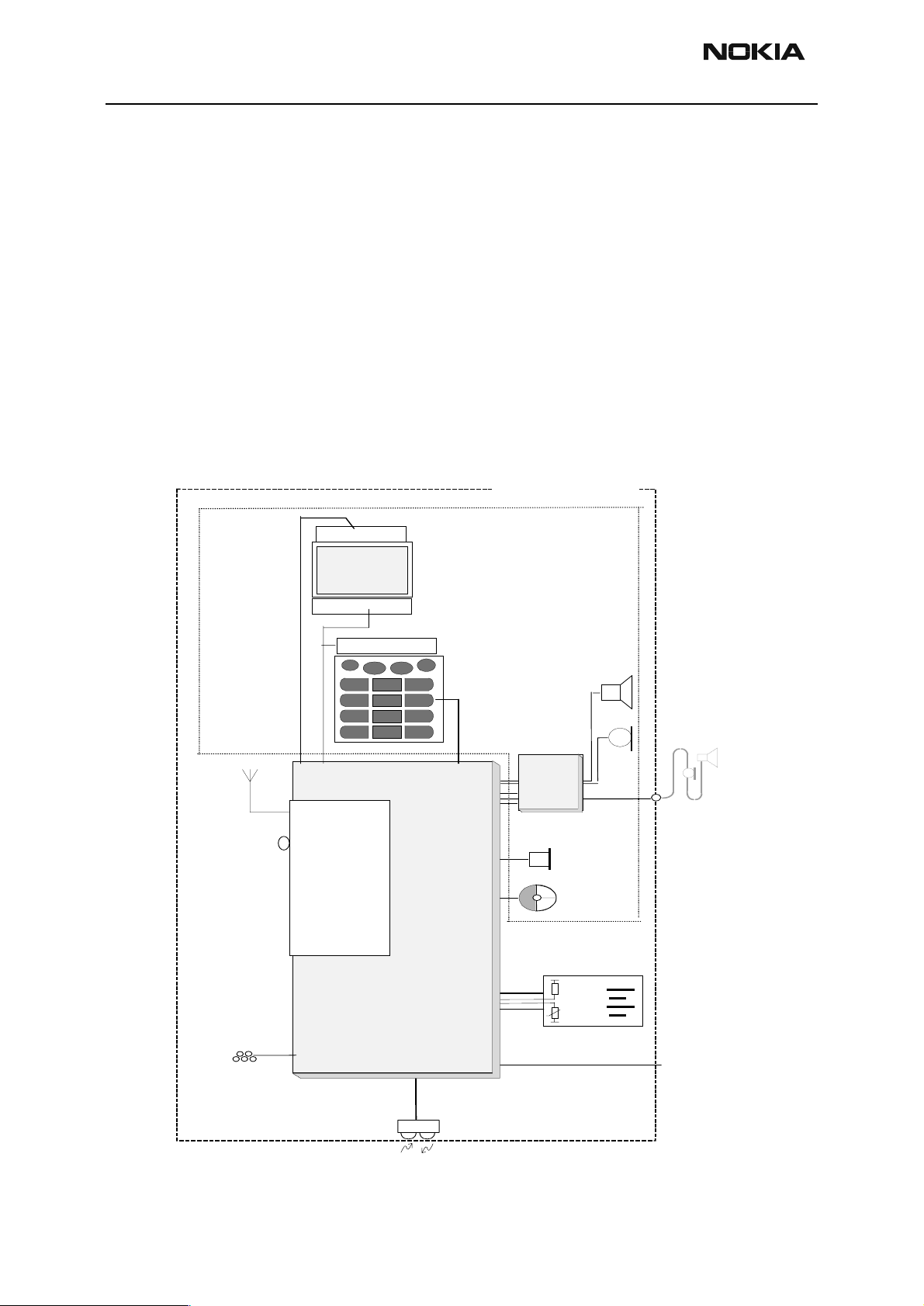
Transceiver NPW-1
Introduction
The NPW-1 is a dual band transceiver unit designed for TDMA800/1900 networks. The
transceiver consists of the engine module (WS8) and the various assembly parts.
The transceiver has a full graphic display and the user interface is based o n a jack style
UI with two soft keys. An internal antenna is used in the phone, and there is no connection to an external antenna. The transceiver also has a low leakage tolerant earpiece and
an omnidirectional microphone that provides excellent audio quality.
An integrated infrared (IR) link provides c onnection betwee n tw o NPW-1 transceiv ers or
between a transceiver and a PC (internal da ta), or a transceiver and a printer.
Figure 1: Interconnect ing Diagram
TRANSCEIVER
ANT
RF Switch
LCD DRIVER
B & W
display
BACKLIGHT
BACKLIGHT
✉
RF
☎
6
9
0#
ENGINE
U S ER IN TE RF A CE
AUDIO
(discr)
BUZZER
VIBRA
MIC
E xt. Aud io
Accesso ries
BB
Pr o d .T E ST I/F
INF RA RE D
Module
BSI
BTemp
BATTERY
CHARGER
Page 8 ãNokia Corporation Issue 1 10/01
Page 9

NPW-1
PAMS Technical Documentation System Module
Operational Modes
Below is a list of the phone’s different ope rational modes:
1 Power Off mode
2 Normal Mode (Power controlled by cellular SW, includes various Active and Idle
states):
• Analog Modes (800 MHz only):
•Analog Control Channel, ACCH
•Analog Voice Channel, AVCH
• Digital Modes (800 and 1900 MHz):
•Control Channel, DCCH
•Digital Voice Channel, DTCH (Digital Traffic Channel)
•Digital Data Channel, DDCH
Both the analog and digital modes have different states c ontrolled by the Cellular
SW. Some examples are Idle State (on ACCH), Camping (on DCCH), Scanning, Con-
versation, NSPS (No Service Power Save, previously OOR = Out of Range).
3 Local mode (both Cellular SW and UI SW non active)
4 Test mode (Cellular SW active but UI SW non active)
Environmental Specifications
Normal and extreme voltages
Voltage range:
• nominal battery voltage: 3.6 V
• maximum battery voltage: 5.0 V
• minimum battery voltage: 3.1 V
Temperature Conditions
Temperature range:
• ambient temperature: -30...+ 60 ×C
• PWB temperature: -30...+85 ×C
Issue 1 10/01 ãNokia Corporation Page 9
Page 10

NPW-1
System Module PAMS Technical Documentation
• storage temperature range: -40 to + 85 ×C
All of the EIA/TIA-136-270A requirements are not exactly specified over the temperature
range. For example, the RX sensitivity requirement is 3dB lower over the –30 - +60 °C
range.
Page 10 ãNokia Corporation Issue 1 10/01
Page 11
NPW-1
V
A
y
UI
T
T
A
X
X
PAMS Technical Documentation System Module
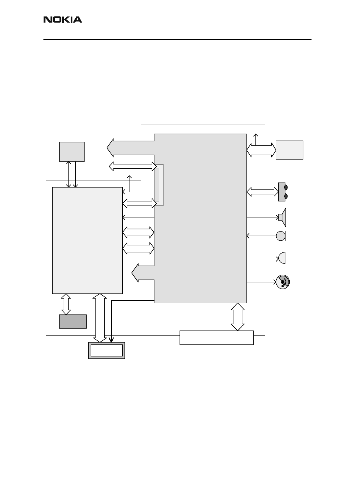
Engine Module
Baseband Module
The core part of the transceiver’s baseband (see the figure below) consists of 2 ASICs, the
UEM and UPP, and flash memory. The following sections illustrate and explain these
parts in detail.
Figure 2: System Block Diagram (simple)
PA suppl
RFIC CTRL
SAFARI
RFCLK
19.44MHz
UPP
RF Supplies
RF RX/T
UEM
PURX
RF RX/T
SLEEPCLOCK
32kHz
CBUS/DBUS
UDIO
IR
EAR
MIC
BUZZER
BATTERY
BB Supplies
IBR
MEMADDA
MEMCON
FLASH
KLIGHT/ DLIGH
PWR ON
BASEBAND
EXTERNAL AUDIO
CHARGER CONNECTION
System Connector
UEM
Introduction to UEM
UEM is the Universal Energy Management IC for digital hand portable phones. In addition to energy management, it performs all the base band’s mixed-signal functions.
Most UEM pins have 2kV ESD protection, and those signals considered to be more easily
exposed to ESD, have 8kV protection within the UEM. These kinds of signals are (1) all
audio signals, (2) headset signals, (3) BSI, (4) Btemp, (5) Fbus and (6) Mbus signals.
Issue 1 10/01 ãNokia Corporation Page 11
Page 12
NPW-1
System Module PAMS Technical Documentation
Regulators
The UEM has six regulators for baseband power supplies and seven regulators for RF
power supplies. The VR1 regulator has two outputs: (1) VR1a and (2) VR1b. In addition to
these, there are two current generators - IPA1 and IPA2 - for biasing purposes.
A bypass capacitor (1uF) is required for each regulator output to ensure stability.
Reference voltages for regulat ors require exter nal 1uF capacitors. Vref25RF is the refer-
ence voltage for the VR2 regulator, Vref25BB is the reference voltage for the VANA,
VFLASH1, VFLASH2, VR1 regulators, Vref278 is the re ference voltage for the VR3, VR4,
VR5, VR6, VR7 regulators, and VrefRF01 is the reference voltage for the VIO, VCORE regulators and for the radio frequency (RF).
Table 1: UEM Regulators
BB RF Current
VANA: 2.78Vtyp 80mAmax VR1a:4.75V 10mAmax
VR1b:4.75V
Vflash1: 2.78Vtyp 70mAmax IPA2: 0-5mA
Vflash2: 2.78Vtyp
40mAmax
VSim: 1.8/3.0V 25mAmax VR3:2.78V 20mA
VIO: 1.8Vtyp
150mAmax
Vcore: 1.0-1.8V
200mAmax
VR2:2.78V 100mAmax
VR4: 2.78V 50mAmax
VR5: 2.78V 50mAmax
VR6: 2.78V 50mAmax
VR7: 2.78V 45mAmax
IPA1: 0-5mA
The VANA regulator supplies the baseband’s (BB) internal and external analog cir cuitry.
It is disabled in the Sleep mode.
The Vflash1 regulator supplie s the LCD, the IR-module and the digital parts of th e UEM
and Safari asic. It is enabled during startup an d goes into the low Iq-mode when in the
Sleep mode.
The VIO regulator supplies both the e xternal and internal logic circuit ries. It is used by
the LCD, flash, bluetooth and UPP. The regulator goes into the low Iq-mode when in the
Sleep mode.
The VCORE regulator supplies the DSP and the core part of the UPP. The voltage is programmable and the startup default is 1.5V. The regulator goes into the low Iq-mode
when in the Sleep mode.
The VSIM regulator supplies the SIM card. NOT USED IN NPW-1.
Page 12 ãNokia Corporation Issue 1 10/01
Page 13

NPW-1
PAMS Technical Documentation System Module
The VR1 regulator uses tw o LDOs and a charge pump. The charge pump requires one
external 1uF capacitor in the Vpump pin and a 220nF flying capacitor between the CCP
and CCN pins. In practice, the 220nF flying capacitor is f ormed by 2 x 100nF capacitors
that are parallel to each other. The VR1 regulator is used by the Safari RF ASIC.
The VR2 regulator is used to supply the (1) external RF parts, (2) lower band up converter, (3) TX power detector module and (4) Safari. In light load situatio ns, the VR2 regulator can be set to the low Iq-mode.
The VR3 regulator supplies the VCTCXO and Safari in the RF. It is always enabled when
the UEM is active. When the UEM is in the Sleep mode, the VR3 is disabled.
The VR4 regulator supplies the RX frontends (LNA and RX mixers).
The VR5 regulator supplies the lower band PA. In light load situations, the VR5 regulator
can be set to the low Iq-mode.
The VR6 regulator supplies the higher band PA and TX amplifier. In light load situations,
the VR6 regulator can be set to the low Iq-mode.
The VR7 regulator supplies the VCO and Safari. In light load situations, the VR7 regulator
can be set to the low Iq-mode.
The IPA1 and IPA2 are programmable current generators. A 27kW/1%/100ppm external
resistor is used to improve the accuracy of the output current. The IPA1 is used by the
lower PA band and IPA2 is used by the higher PA band.
RF Interface
The interface between the baseband and the RF section is also handled by the UEM. It
provides A/D and D/A conversion of the in-pha se and quadrature receive and transmit
signal paths. It also provides A/D and D/ A conve rsions of receiv ed and transmitte d audio
signals to and from the UI section. The UEM supplies the analog AFC signal to the RF section, according to the UPP DSP digital control.
Charging Control
The CHACON block of the UEM asics controls charging. The needed functions for the
charging controls are the (1) pwm-controlled battery charging switch, (2) charger-monitoring circuitry, (3) battery voltage monitori ng circuitry and (4) RTC supply circuitry for
backup battery charging (Not used in NPW-1). In addition to these, external components
are needed for EMC protection of the charger input to the baseband module.
Digital Interface
Data transmission between the U EM and the UPP is impleme nted using two seri al connections, DBUS (programmable clock) for DSP and CBUS (1.0MHz GSM and 1.08MHz
TDMA) for MCU. The UEM is a dual voltage circuit: the digital parts are run from 1.8V
and the analog parts are run from 2.78V. The Vbat (3,6V) voltage regulators's input is
also used.
Issue 1 10/01 ãNokia Corporation Page 13
Page 14

NPW-1
System Module PAMS Technical Documentation
Audio Codec
The baseband supports two external microphone input ar eas and one external ea rphone
output. The input can be taken from an internal microphone, a headset microphone or
from an external microphone signal source through a headset connector. The output for
the internal earpiece is a dual-ended type output, and the dif ferential output is capable
of driving 4Vpp to the earpiece with a 60 dB minimum signal as the total distortion ratio.
The input and output signal source se lection and gain control is performed inside the
UEM Asic, according to the c ontrol messages from the UPP. A buzzer a nd an external
vibra alert control signal are gener ated by the UEM with separate PWM outputs.
UI Drivers
There is a single output driver for the buzzer, vibra, display and keyboard LEDs and the IR
in the side of the UEM. These generate PWM square wave for the various devices.
IR interface
The IR interface is designed and implemented into th e UEM. The low frequency mode of
the IR module covers speeds up to 115.2 kbit/s. The device (Vis hay) tr ansc eiv ers inte gra te
a sensitive receiver and a built-in power driver. The combination of a thin, long resistive
and inductive wiring should be avoided. The input (Txd, SD/M ode) and the output Rxd
should be directly coupled to the I/O circuit. The VBAT regulator supplies the power to
transmit the LED and serial resistor limits’ current. Upon receiving infrared data to IR
LED, it goes straight to the UEM via the RXD line. The Vflash1 is the power supply for the
IR module, except for transmission.The IR module has one control pin to control the shut
down. The control lever shifter is used to change the proper voltage for shutdown to the
IR module from the UPP.
AD Converters
The UEM is equipped with a 11-channel analog to digital converter. Some AD converter
channels (LS, KEYB1-2) are not used in NPW-1. The AD converters are calibrated in the
production line.
UPP
Introduction
NPW-1 uses the UPPv4M ASIC. The RAM size is 4M. The processor architecture consists
of both the DSP and the MCU processors.
Blocks
The UPP is internally partitioned into two main parts: (1) the Brain and (2) the Body.
1 The Processor and Memory System (that is, the Processor cores, Mega-cells,
internal memories, perip herals and external memory inter face) is known as the
Brain.
The Brain consists of the following blocks: (1) the DSP Subsystem (DSPSS), (2) the
MCU Subsystem (MCUSS), (3) the emulation control EMUCtl, (4) the program/
data RAM PDRAM and (5) the Brain Peripherals–subsystem (BrainPer).
Page 14 ãNokia Corporation Issue 1 10/01
Page 15

NPW-1
PAMS Technical Documentation System Module
2 The NMP custom cellular logic functions are known as the Body.
The Body contains interfaces and functions needed fo r interfacing other baseband and RF parts. The body consists of, fo r example, the following sub-blocks:
(1) MFI, (2) SCU, (3) CTSI , (4) RxModem, ( 5) Acc IF, (6) UIF, (7) C oder, (8) BodyIF, (9)
PUP.
Flash Memory
Introduction
The NPW-1 transceiver uses a 32 Mbit flash as its e xte rnal memor y. The VIO regulator is
used as a power supply for normal in-system op eration. An accelerated program/erase
operation can be obtained by supplying Vpp of 12 volt to the flash device.
The device has two read modes: asynchronous and burst. The Burst read mode is utilized
in NPW-1, except for the start-up, when the asynchronous read mode is used for a short
time.
Issue 1 10/01 ãNokia Corporation Page 15
Page 16
NPW-1
System Module PAMS Technical Documentation
User Interface Hardware
LCD
Introduction
NPW-1 uses a black & white GD46 84x48 full dot matrix graphical display . There are two
suppliers for this LCD: Seiko Epson and Philips. The LCD module includes the LCD glass,
the LCD COG-driver, an elastomer connector and a metal frame. The LCD module is
included in the lightguide assembly module.
Interface
The LCD is controlled by the UI SW and the control signals are from the UPP asic. The VIO
and Vflash1 regulators supply the LCD with power.
The LCD has an internal voltage booster and a booster capacitor is required between
Vout and GND.
Pin 3 (Vss9) is the LCD driver’s ground and Pin 9 (GND) is used to ground the metal
frame.
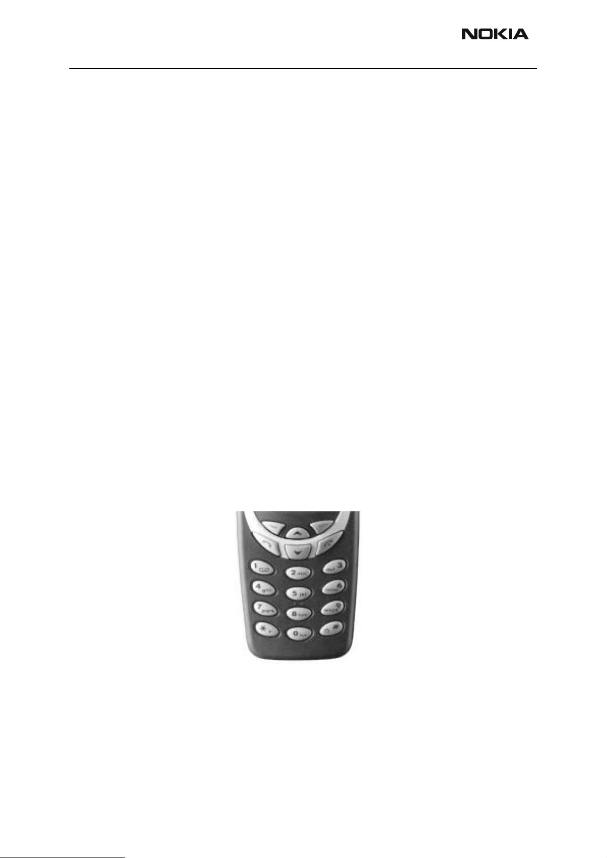
Keyboard
Introduction
The NPW-1 keyboard style follows the Nokia Jack style, without side keys for volume
control. The PWR key is integrated so that it is part of the IR window and located on top
of the phone.
Figure 3: Placement of keys.
Power Key
All signals for the keyboard come from the UPP asic, except PWRONX line for the power
key signal which is connect ed dir ectly to t he U EM. The pr essing o f the PWR k ey gro und s
the PWRONX line and the UEM generate s an inter rupt to U OO, which is then re cognized
as a PWR key press.
Page 16 ãNokia Corporation Issue 1 10/01
Page 17

NPW-1
PAMS Technical Documentation System Module
Keys
Other keys are detected so that w hen a key is pressed down, the metal dome connects
one S-line and one R-line of the UPP to the GND and creat es an interrupt for the SW.
This kind of detection is also known as metaldome detection. The matrix of how lines are
connected and which lines are used for differen t keys is described in the Table 1. The Sline S0 and R-line R5 are not used at all.
Table 2: Matrix of Key Detection Lines
S0 S1 S2 S3 S4
Returns /
Scans
R0 NC NC Send End NC
R1 NC Soft left Up Down Soft right
R2 NC 1 4 7 *
R3 NC 2 5 8 0
where NC = Not Connected
Lights
Introduction
NPW-1 has 10 LEDs for lighting purposes. Six of them are for the keyboard and four for
the display. The LED type is Osram LGM470, green light emitting and SMD through hole
mounted.
Interfaces
The display lights are controlled by a Dlight signal from the UEM. The Dlight output is the
PWM signal, which is used to control the average current going through the LEDs. When
the battery voltage changes, the new PWM v alue is written onto the PWM register. In
this way, the brightness of the lights remains the same with all battery voltages within
range. The frequency of the signal is fixed at 128Hz.
The keyboard lights are controlled by the Klight signal from the UEM. The Klight output is
also a PWM signal and is used in the same way as Dlight.
R4 NC 3 6 9 #
R5 NC NC NC NC NC
Technical Information
Each LED requires a hole in t he PWB, in which the body of the LED locates in hole and
terminals are soldered on the component side of the module PWB. The LEDs have a white
plastic body around the diode, and this directs the emitted light better to the UI-side.
The current for the LCD lights is limited by the resistor between the Vbatt and LEDs. For
the keyboard lights there are resistors in parallel.
Issue 1 10/01 ãNokia Corporation Page 17
Page 18

NPW-1
System Module PAMS Technical Documentation
Vibra
Introduction
The vibra is located on the D-cover and is connected by spring connectors on the bottom
left-hand side of the engine. The vibra motor is supplied by Namiki.
Interfaces
The vibra is controlled by the PWM signal VIBRA from the UEM. With this signal, it is
possible to control both the frequency and pulse width of the signal. The pulse widt h is
used to control the current when the bat tery vol tage changes. Wit h the freque ncy control, it is possible to search for the optimum frequency to have silent and efficient vibrating.
Table 3: Electrical Parameters
Parameter Requirement Unit
Rated DC Voltage 1.3 V
Rated speed
Rated current
Starting current
Armature resistant 8.6 ohm
Rated DC voltage being able to use 1.2 to 1.7 V
Starting DC voltage min. 1.2 V
9500 ±3000
115 ±20
150 ±20
rpm
mA
mA
Page 18 ãNokia Corporation Issue 1 10/01
Page 19

NPW-1
PAMS Technical Documentation System Module
Audio HW
Earpiece
Introduction
The Philips Speaker System 13mm speaker capsule is used in NPW-1.
The speaker is a dynamic one. It is very sensitive and capable of producing relatively high
sound pressure also at low frequencies. The speaker capsule and the mechanics around it
together make the earpiece.
Microphone
Introduction
The microphone is an electret microphone with an omnidirectional polar pattern. It consists of an electrically polarized membrane and a metal electrode which form a capacitor .
Air pressure changes (for example, sound) moves the membrane, which causes voltage
changes across the capacitor. Because the capacitance is t ypically 2 pF, a FET buffer is
needed inside the microphone capsule for the signal generated by the capacitor. Because
of the FET, the microphone needs a bias voltage.
The microphone manufacturers for the NPW-1 transceiver are Matsushita and Hosiden.
Buzzer
Introduction
The operating principle of the buzzer is magnetic. The diaphragm of the buzzer is made
of magnetic material and it is located in a magnetic f ield created by a perm anent magnet. The winding is not attached to the diaphragm, as is the case with the speaker. The
winding is located in the magnetic circuit so tha t it can alter the magnetic field o f the
permanent magnet, thus changing the magnetic force affecting the diaphragm. The
buzzer's useful frequency range is approximately from 2 kHz to 5kHz.
The Buzzer manufacturer for the NPW-1 transceiver is Star.
Issue 1 10/01 ãNokia Corporation Page 19
Page 20

NPW-1
UEM
Ni-MH
VBATT
GND
BTEMP
Battery
System Module PAMS Technical Documentation
Battery
Phone Battery
Introduction
The BMC-2 battery (Ni-MH 640mAh) is be used in the NPW-1 transceiver by default. It is
also possible to use the BMC-3 (Ni-MH 900mAh) and BLC-2 (Li-ion 850mA) batteries.
Interface
The battery block contains NTC and BSI resistors for tempe rature measur emen t and battery identification. The BSI fixed resistor value indicates the chemistry and default
capacity of a battery. The NTC-resistor measures the battery temperature. Temperature
and capacity information is needed for charge control. These resistors are connected to
BSI and BTEMP pins of the battery connector. The phone has pull-up resistors for these
lines so that they can be re ad by A/D inputs in the phone (see the figure below). Serial
resistors in the BSI and BTEMP lines are f or ESD protection. Both lines also have spark
caps to prevent ESD.
C220
1n
C217
1n
R202/1
100k
R205/1
10k
R205/2
10k
Figure 4: Battery Connection Di agram
VFLASH1VANA VBAT
R202/4
100k
connector
C100
10p
BSI
OVERCHARGE/
OVERDISCHARGE
PROTECTION
The batteries have a specific red line, which indicates if the battery has been subjected to
excess humidity. The batteries are delivered in the protection mode, which gives longer
storage time. The voltage seen in the outer terminals is zero (or floating), and the battery
is activated by connecting the charge r. The battery has internal protection for overvoltage and overcurrent.
Page 20 ãNokia Corporation Issue 1 10/01
Page 21

NPW-1
1 (+)
2(BSI)
3(BTEMP)
4(GND)
PAMS Technical Documentation System Module
Figure 5: BMC-2 Battery contacts (BMC-3, BLC-2 have same interface).
Battery Connector
NPW-1 uses the spring type battery connector. This makes the phone easier to assemble
in production and the connection between the battery and the PWB is more reliable. The
battery connector is manufactured by Molex.
Table 4: Battery Connector Interface
# Signal
name
1 VBAT (+)
2 BSI BSI
3 BTEMP BTEMP
4 GND GND GND GND
Connected from - to Batt.
I/O
VBAT I/O Vbat 3.0-5.1V Battery
(batt.)
UEM Out Ana Battery size
(batt.)
UEM Out Ana 40mA/
(batt.)
Signal properties
A/D--levels--freq./timing
Gns
Switch
400mA
Description /
Notes
voltage
indicator
Battery
temperature
indicator
Ground
Issue 1 10/01 ãNokia Corporation Page 21
Page 22

NPW-1
PWMOUT(GND)
System Module PAMS Technical Documentation
Accessories Interface
System connector
Introduction
NPW-1 uses accessories via a system connector.
Interface
The interface is supported by fully differential 4-wire (XMICN, XMICP, XEARN and
XEARP) accessories. NPW-1 supports the HDC-5 headset, LPS-3 loopset and the PPH-1
car kit.
Figure 6: System Connector
GND
VIN
XMICN
XEARN
MICP
An accessory is detected by the HeadInt- li ne, which is connected to the XEARP inside
the system connector. When an accessory is connected, it disconnects XEARP from
HEADINT, and the UEM detects it and generates an interrupt (UEMINT) to the MCU. After
that, the HOOKINT line is used to determine whic h accessory is connected. This is done
by the voltage divider, which consists of the phone's internal pull-up and accessory-specific pull-down. The voltage generated by this divider is then read by the ad- converter of
UEM. The HOOKINT- interrupt is generated by the button in the headset or by the accessory external audio input.
XMICP
XEARP
HEADINT
MICN
Page 22 ãNokia Corporation Issue 1 10/01
Page 23

NPW-1
MicGnd
PAMS Technical Documentation System Module
Figure 7: Accessory Detection / External Audio.
2.7V
Hookint
/MBUS
EAD
HeadintHeadint
MIC1&3 Bias
MIC1P
MIC1N
HF
HFCM
3...25k
UEM
Technical Information
ESD protection is made up by (1) spark caps, (2) a buried capacitor (Z152 and Z154-157)
and (3) ±8kV inside the UEM. The RF and BB noises are prevented by inductors.
PPH-1 Handsfree
Introduction
The PPH-1 handsfree device
2.1V
33N
0.8V
33N
1k2
1.8V
0.3V
1k2
• provides the charging and handsfree functionality
• has a built-in speaker
• and uses a phone microphone, but also has a connector for t he HFM-8 optional
external microphone (using HFM-8 mutes phone microphone)
Interface
A 4-wire interface is implemented with 2.5mm diame ter round plug/jack which is otherwise like a so-called standard stereo plug, but th e innermost contact is split into two.
Issue 1 10/01 ãNokia Corporation Page 23
Page 24

NPW-1
System Module PAMS Technical Documentation
Figure 8: 4-wire, fully differential headset connector pi n layo ut
2. XEARN
4. XEARP
5. H EADINT
3. XMIC P
1. XMIC N
IR module
Introduction
The IR module integrates a sensitive receiver and a built-in power driver complaint to the
IrDA 1.2 standard. The IR module is located at the top of the engine side, nex t to the
Power switch.
The IR module manufacturer for the NPW-1 transceiver is Vishay.
Interface
The Vflash1 regulator supplies the IR module, except for the transmit LED. The transmit
LED is supplied by the VBAT regulator and the maximum current is limited by a se rial
resistor. The bypass capacitor is needed in the VBAT line for proper voltage. TXD and RXD
lines are connected to the UEM and shutdown is controlled by the UPP (GENIO(10))
through a level-shifter V350.
Technical Information
The IR interface is located in the UEM. The IR link supports speeds fr om 9600 bit/s to
1.152 MBit/s, up to 1m.
Charger IF
Introduction
The charger connection is implemente d through the system connector. The system connector supports charging with both plug chargers and desktop stand chargers.
There are three signals for charging. The cha rger GND pin is used for both desktop and
plug chargers as well as for charger voltage. The PWM cont rol line, which is needed for
3-wire chargers, is connected directly to the GND in the PWB module, so the NPW-1
engine does not provide any PWM control for chargers. Charging controlling is done
inside the UEM by switching the UEM’s intern al charger switch on and off.
Page 24 ãNokia Corporation Issue 1 10/01
Page 25

NPW-1
PAMS Technical Documentation System Module
Interface
The fuse F100 protects the phone from too high currents, for example, when broken or
pirate chargers are used. L100 protects the engine from RF noises, which may occur in
the charging cable. V100 protects the UEM ASIC from reverse polarity charging voltage
and from too high charging voltages. C106 is also used for ESD and EMC protection.
Spark gaps right after the charger plug are used for ESD protection.
Issue 1 10/01 ãNokia Corporation Page 25
Page 26

NPW-1
VPP
FBUS_TX
X
System Module PAMS Technical Documentation
Test Interfaces
Production Test Pattern
The interface for NPW-1 production testing is a 5pin pad layout in the BB area (see the
figure below). The production tester conne cts to these pads by using spring connectors.
The interface includes the MBUS, FBUSRX, FBUSTX, VPP and GND signals. The pad size i s
1.7mm. The same pads are used also for AS test e quipment, such as the module jig and
the service cable.
Figure 9: Top View of Production Test Pattern
Other Test Points
As BB asics and flash memory are CSP components, the visibility of BB signals is very
poor. This makes the measuring of most of the BB signals impossible. In order to debug
the BB, at least to some level, the most important signals can be accessed from the
0.6mm test points. The figure below shows the test points located between the UEM and
the UPP. There is an opening in the baseband shield to provide access to these pads.
2.
6.
3. FBUS_RX
8. GND
7.
MBUS
Figure 10: Test points Located Between UEM and UPP
UE M (D200)
CBUSDA
J407
J405
UPP (D400)
CBUSENX
J408
J415
DBUSEN1X
CBUSCLK
J406
J412
FBUS RX
FBUS TX
J411
J409
MBUSTX MBUSR
J410
J414
DBUSCLKDBUSDA
J403
J413
J402
PURXSLEEPX
SLEEPCLK
J404
UEMINT
Page 26 ãNokia Corporation Issue 1 10/01
Page 27

NPW-1
PAMS Technical Documentation System Module
EMC
General
The EMC performance of NPW-1’s baseband is impr oved by using a shield to cover the
main components of the BB, such as the UEM, UPP and Flash. The UEM has internal protection against a ±8kV ESD pulse. The BB-shield is soldered to the PWB and it also
increases the rigidity of the PWB in the BB area, thus improving the phone’s reliability.
The shield also improves the thermal dissipation by spreading the heat more widely.
The BB and RF shield are connected together on the PWB and the protective metal deck
underneath the battery is grounded to RF shield.
BB Component and Control IO Line Protection
Keyboard lines
ESD protection for keyboard signals is implemented by using metaldome detection.
Grounded keydomes are very eff ective for ESD protectio n and do not require additional
components for ESD protection. The distance from the A-cover to the PWB is made
longer using spikes in the key mat. The C-cover metalliza tion also protects th e keyboard
lines.
C-Cover
The C-cover on the UI-side is metallized on the inne r sur face (partl y) and is gro unded to
the GND module. All areas in which the plated C-cover touches the PWB surface are
grounded and the solder masks are opened.
PWB
All edges are grounded on both sides of the PWB and the solder mask is opened in these
areas. The aim is that any ESD pulse faces the ground area when enter ing the phone, for
example, between the mechanics covers.
All holes in the PWB are grounded and plated through holes. The only exception i s the
LED holes, which cannot be grounded.
LCD
ESD protection for LCD is implemented by connecting the metal fr ame of the LCD into
ground. The connection is only on one side, at the top of the LCD, which is not the best
solution. The software takes care of the LCD's crashing in case of an ESD pulse.
Microphone
The microphone’s metal cover is connected to the GND and ther e are spark gaps on the
PWB. The microphone is an asymmetrical circuit, which makes it w ell protected against
EMC.
EARP
The EARP is protected with C-cover metallization and with a plastic-fronted earpiece.
Issue 1 10/01 ãNokia Corporation Page 27
Page 28

NPW-1
System Module PAMS Technical Documentation
Buzzer
PWB openings with the C-cover metallization protect the buzzer from ESD.
IRDA
PWB openings with C-cover metallization protect IRDA lines fr om ESD.
System Connector Lines
Table 5: System Connector lines
System Connector signals that have EMC protection
Protection type VIN XMIXP XMICN XEARP XEARN HEADINT MICP
ferrite bead (600
/199MHz)
ferrite bead (420
/100MHz)
spark gaps XXXXXX
PWB capacitors XXXXXX
RC-circuit X X X X X
capacitor to
ground
X
XXXXX
XXXX X
Battery Connector Lines
BSI and BTEMP lines are protected by spark gaps and the RC-circuit (10k & 1n), in which
the resistors are size 0603.
MBUS and FBUS
The opening in the protective met al deck, underneath the battery, is so small that ESD
does not get into the MBUS and FBUS lines in the producti on test pattern.
Page 28 ãNokia Corporation Issue 1 10/01
Page 29

NPW-1
PAMS Technical Documentation System Module
Transceiver Interfaces
The tables in the following sections illustrate the signals between the various transceiver
blocks.
BB - RF Interface Connections
All the signal descriptions and prope rt ies in th e following table s ar e valid only f or act ive
signals, and the signals are not necessarily present all the time.
Note: In the following tables, the nominal signal level of 2.78V is sometimes referred
to as 2.7V.
Table 6: BB - RF Interface Signal Description
RIP Signal name Connected
from - to
RFICCNTRL(2:0) RF IC Control Bus from UPP to RF IC (SAFARI)
0 RFBUSCLK UPP RFIC In Dig 0/1.8V
1 RFBUSDA UPP/
RFIC
2 RFBUSEN1X UPP RFIC In Dig RFIC Chip Set X
PUL (2:0) Power Up Reset from UEM to RF IC (SAFARI)
0 PURX UEM RFIC Out Dig 0/1.8V 10us Power Up Reset for RFIC
GEN (28.0) General I/= Bus connected to RF, see also sepa rate collective
5TXP1 RFIC,
Loband
mixer
6 TXP2 RFIC UPP Out Dig 0/1.8V High band Tx enabled
RFIC
UPP
UPP Out Dig 0/1.8V 10 us Low Band Tx enabled
BB I/O Signal Properties
A/D Levels-Freq./
Timing resolution
9.72
(0: <0.4V
I/O Dig Bi-directional RF Control serial
GEN(28.0) table
Control lines from UPP GENIOs to RF
1: >1.4V
MHz
Description / N otes
RF Control serial bus bit clock
bus data.
SLCLK & SLEEPX not used in RF
RFCLK (not BUS -> no rip #) System Clock from RF to BB, original source VCTCXO, buffer ed (and
frequency shifted, WAM only) in RF IC (SAFARI)
RFCLK VCTCX
O ->
RFIC
RFClk
GND
SLOWAD(6:0) Slow Speed ADC Lines from RF block
RF UPP In Ana 0 System Clock slicer Ref GND,
UPP In ANA 800mVpp
typ (FET
probed)
Bias DC
blocked at
UPP input
19.44
MHz
System Clk from RF to BB
not separated from pwb GND
layer
Issue 1 10/01 ãNokia Corporation Page 29
Page 30

NPW-1
System Module PAMS Technical Documentation
RIP Signal name Connected
from - to
5PDMID RF
Power
detection
module
6PATEMP RF
Power
detection
module
RFCONV(9:0) RF-BB differential Analog Sig nals: Tx I& Q, Rx I&Q and refer ence volt -
0 RXIP RFIC UEM In Ana 1.4Vpp max .
1RXIN
2 RXQP Diff. positive/negative quadra3RXQN
UEM In Ana 0/2.7V dig 0/VR2 Power detection module identi-
UEM In Ana 0.1-2.7V - Tx PA Temperature to UEM, NTC
BB I/O Signal Properties
A/D Levels-Freq./
Timing resolution
ages
diff. 0.5Vpp
typ bias
1.30V
Description / N otes
fication to slow ADC (ch 5, previous VCTCXO Temp) signal to
UEM
in Power Detection Module
Differential positive/negative
in-phase Rx Signal
ture phase Rx Signal
4 TXIP UEM RFIC Out Ana 2.2Vpp max.
5TXIN
6 TXQP Diff. positive/negative quadra7TXQN
9 VREFRFO1 UEM RFIC Out Vref 1.35 V RF IC Reference voltage from
RFAUXCON(2:9) RF-BB Analog Control Signals to/from UEM
1 TXPWRDET TXP
Det.
2AFC UEMVCTCXOOut Ana 0.1-2.4V Automatic Frequency Control
VRF Globals instead of Bus Regulated RF Supply Voltages from UEM to RF. Current values are of
VR1 A UEM RFIC Out Vreg 4.75 V
VR1 B UEM RFIC Out Vreg 4.75 V
UEM In Ana 0.1-2.4V 50 us Tx PWR Detector Signal to UEM
the regulator specific ations, not the measured values of RF
diff. 0.6Vpp
typ bias
1.30V
+- 3%
+- 3%
10mA
max.
10mA
max.
Differential positive/negative
in-phase Tx Signal
ture phase Tx Signal
UEM
for VCTCXO
UEM, charge pump + linear
regulator output. Supply for
UHF synth phase det...
UEM, charge pump + linear
regulator output. Supply for Tx
VHF VCO.
VR2 UEM RFDisc
r./RFIC
VR3 UEM VCTCXOOut Vreg 2.78 V
Out Vreg 2.78 V
+- 3%
+- 3%
100
mA
max.
20mA
max.
UEM linear regulator. Supply
voltage for Tx IQ filter and IQ to
Tx IF mixer.
UEM linear regulator. Power
supply to VCTCXO + RFCLK
Buffer in RF IC.
Page 30 ãNokia Corporation Issue 1 10/01
Page 31

NPW-1
PAMS Technical Documentation System Module
RIP Signal name Connected
from - to
VR4 UEM RFIC Out Vreg 2.78 V
VR5 UEM RFIC Out Vreg 2.78 V
VR6 UEM RFIC Out Vreg 2.78 V
VR7 UEM RFIC,
UHF
VCO
IPA1 UEM RF PA Out Iout 0-5 mA Settable Bias current for RF PA
IPA2 UEM RF PA Out Iout 0-5 mA Settable Bias current for RF PA
VFLASH1 UEM RFIC Out Iout 2.78V 12mA UEM linear regulator common
BB I/O Signal Properties
A/D Levels-Freq./
Timing resolution
+- 3%
+- 3%
+- 3%
Out Vreg 2.78 V
+- 3%
Description / N otes
50mA
max.
50mA
max.
50mA
max.
45mA UEM linear regulator. Power
UEM linear regulator. Power
supply for LNA/RFIC Rx chain.
UEM linear regulator. Power
supply for RF low band PA
driver section.
UEM linear regulator. Power
supply for RF high band PA
driver section.
supply for RF Synthes.
L-Band
H-Band
for BB. RFIC digital parts and F
to BB digl. IF.
VBATT, Global
VBATTRF Batt
Conn
RFPA Out Vbatt3...5V 0...1A
2A
peak
Raw Vbatt for RF PA
BB Internal Connections
UEM Block Signal Description
Table 7: UEM Block Signals to UPP
RIP Signal name Connected
from - to
RFCONVDA(5:0)* 1.8V digital interface between UPP and UEM. R F conv erter CLK. Rx and Tx
0RFCONVCLKUPP UEMInDig0/1.8V 4.86
1 RXID UEM UPP Out (PDM) RxI Data
2RXQD
UEM I/O Signal Properties
A/D Levels-Freq./
Timing resolution
I&Q data (bit stream signals).
Description / Notes
RF Converter Clock
MHz/ Digi
3.24 MHz
/ Ana
(PDM) RxQ Data
3 TXID UPP UEM In (PDM) TxI Data
4TXQD
5 AUXDA UPP UEM In Auxiliary DAC Data
(PDM) TxQ Data
Issue 1 10/01 ãNokia Corporation Page 31
Page 32

NPW-1
System Module PAMS Technical Documentation
RIP Signal name Connected
from - to
RFCONVCTRL(2:0)* 1.8V digital interface be tween UP P (DSP ) and UEM. RF c onverte r UEM RF
0DBUSCLK UPP UEMInDig0/1.8V 9.72MHz Clock for Fast Control to UEM
1DBUSDA In/
2 DBUSENX In Fast Control Data Load / Enable
AUDUEMCTRL(3.0)* 1.8V digital interface betw een U PP (M CU) a nd UE M. Bid ire ct ional Con trol
0 UEMINT UEM UPP Out Dig 0/1.8V UEM Interrupt
1 CBUSCLK UPP UEM In 1.08MHz Clock for control/Audio Con-
2CBUSDA In/
3 CBUSENX In Control Data Load Signal
AUDIODA T A(1:0)* 1.8V digital au dio interfac e between UPP and UEM audio co dec. PDM data
UEM I/O Signal Properties
A/D Levels-Freq./
Timing resolution
IF bidirectional serial Control Bus, “DBUS”.
Out
Bus “CBUS”
1.08Mbit/sControl data
Out
clocked by CBUSCLK
Description / Notes
Fast Control Data to/from UEM
to UEM
vertors in UEM
0 EARDATA UPP UEM In Dig 0/1.8V 1.08Mbit/sPDM Data for Downlink Audio,
clocked by CBUSCLK
1 MICDATA UEM UPP Out PDM Data forUplink Audio,
clocked bu CBUSCLK
PUSL(2:0)* Power-U p & Slee p Control lines
0 PURX UEM UPP
RFIC
1 SLEEPX UPP UEM In Power Save Functions, 0 at
2 SLEEPCLK UEM UPP Out 32 KHz 32 KHz Sleep Clock
IACCDIF(5:0)* BB Internal 1.8V Digital Accessory Buses between UPP and 2.7V level
0IRTX
IRRX
1
2MBUSTX
MBUSRX
3
4FBUSTXI
FBUSRXI
5
UPP
UEM
UPP
UEM
UPP
UEM
UEM
UPP
UEM
UPP
UEM
UPP
Out Dig 0/1.8V Power Up Reset, 0 at reset
sleep
shifter UEM
OutInDig 0/1.8V 1.152
Mbit/s
max
In
Dig 0/1.8V 9k6 b/s
Out
In
Dig 0/1.8 V <115kb/s
Out
9k6 b/s
< 7 Mb/s
<1Mb/s
<115kb/s
<7Mb/s
Infrared Transmit
Infrared Receive
MBUS Transmit
MBUS Receive / FDL Clk
FBUS Transmit / FDL Tx
FBUS Receive / FDL Rx
Page 32 ãNokia Corporation Issue 1 10/01
Page 33

NPW-1
PAMS Technical Documentation System Module
Table 8: UEM Block Signals to BB and RF
RIP Signal name Connected
from - to
SLOWAD(6:0)* SLow Speed ADC Lines, UEM extern al
0BSI BAT1BTEMP
5PDMid RF
6PATEMP RF,
RFCONV(9:0)* RF - BB Analog Signals: Tx I&Q, Rx I&Q and ref
0 RXIP RFIC UEM In Ana 1 .4Vpp max
1RXIN
2 RXQP Diff. positive/negative quadra3RXQN
4 TXIP UEM RFIC Out Ana 2.2Vpp max
5TXIN
6 TXQP Differential positive/negative
7TXQN
TERY
PDMod
PDMod
NTC
UEM In Ana 0-2.7V Battery Size Indicator/FDL init
UEM In Ana 0-2.7V Power detection modul e identi-
UEM I/O Signal Properties
A/D Levels-Freq./
Timing resolution
diff.
0.5Vpp typ
bias 1.30V
diff.
0.6VppTyp
Bias 1.30V
Description / Notes
Battery Temperature
fication to slow ADC (ch, previous VCTCXO Temp) signal to
UEM.
Differential positive/negative
in-phase Rx Signal
ture phase Rx Signal
Differential positive/negative
in-phase Tx Signal
quadrature phase Tx Signal
9 VREFRFO1 UEM RFIC Out Vref 1.35V RF IC Reference voltage from
UEM
HP INTERNAL AUDIO
AUDIO(4:0) HP Internal analog ear & microphone IF between UEM and Mic/Ear circuitry
0 EARP UEM Ear1EARN
2 MIC1N Mic UEM In Ana 100mVpp
3MIC1P
4MICB1 Mic UEMOutV
EXTERNAL AUDIO INTERFACE
XAUDIO(9:0)* Ex ternal Audio IF between UEM and X-audio circuitry
0 HEADINT SysCon
/HSet
1 HF UEM SysCon
2 HFCM Ana 0.8 Vdc
piece
UEM In Dig 0/2.7V Input for Headset Connector
/HSet
Out Ana 1.25V Audio Differential sig nal t o HP in t er-
nal Earpiece.
Load resistance 32 ohm.
Audio Differential signal from HP
max diff.
2.1V typ./
bias
<600 uA
Out Ana 1.0Vpp
bias 0.8V
DC Bias Bias voltage for internal MIC
Audio External Earpiece Audio Signal
internal MIC, 2mV nominal
HeadInt Switch
Reference output for DC coupled external Earpiece
Issue 1 10/01 ãNokia Corporation Page 33
Page 34

NPW-1
System Module PAMS Technical Documentation
RIP Signal name Connected
from - to
3 MICB2 UEM SysCon
/HSet
4MIC2P
MIC2N
5
6HOOKINT Sys
CHARGER INTERFACE
CHARGER lines, no bus*
VCHARGIN ChargerUEM In Vchr < 16 V
GND GND GND from/to Charger connec-
PWRONX * Power On Signal, see also the UI/keyboard
SysCon
/Headset
Con
UEM In Ana 200mVpp
UEM In Ana/
UEM I/O Signal Properties
A/D Levels-Freq./
Timing resolution
Out V
2.1V typ/ 600
bias
uA
max diff
0...2.7V DC HS Button interrupt, External
Dig
<1.2 V
Description / Notes
Bias voltage for external MIC
Audio Differential signal from exter-
nal MIC
Audio Accessory Detect (EAD)
DC Vch from Charger Connector,
max. 20 V
tor
PWRONX UI UEM In Dig 0/Vbatt Power button
GND GND GND from/to Charger connec-
tor
RFAUXCONV(2:0) RF-BB auxiliary analog signals
0
1TXPWRDET TXPow.
Det.
Mod.
2 AFC UEM VCTCXOOut Ana 0.1-2.4V 11bits AFC control voltage to VCTCXO,
IRIF, no bus no rips UEM 2.7V signals to IR Module
IRLEDC UEM IR Out Dig 0/2.7V 9k6 -
IRRXN IR UEM In Dig 0/2.7V 9k6 -
UIDRV lines, no bus UEM drivers: sinking outputs to Buzzer, Vibra, KLED, DLED
BUZZO UEM Buzzer Out Dig 350mA max. /
UEM In Ana 0.1-2.7V Tx PWR Detector Output to
UEM
default about 1.3V
IR Tx signal to IR Module
1Mbit/s
IR Receiver signal from IR Mod-
Vbatt
1Mbit/s
1-5 kHz,
PWM vol
ule
Open collector sink switch output for Buzzer. Frequency controlled pitch, PWM for volume.
VIBRA UEM Vibra Out Dig 135mA max /
Vbatt
DLIGHT UEM UI Out Dig 100mA /
Vbatt
64/128/
256/512
Hz
Switch/
100Hz
pwm
Open collector sink switch/Frequency/ pwm output for buzzer
Open drain switch/pwm output
for display light
Page 34 ãNokia Corporation Issue 1 10/01
Page 35

NPW-1
PAMS Technical Documentation System Module
RIP Signal name Connected
from - to
KLIGHT UEM UI Out Dig 100mA /
ACCDIF lines, no bus * Wired Digital Accessory Interface, only to test pattern
MBUS UEM Test
Pad 7
FBUSTXO UEM Test
Pad 2
FBUSRXO Test
Pad 3
RTCBATT lines, no bus * Connector pads for Real Ti me Clock back up battery
VBACK UEM RTC-
GND Global GND 0
VBB, Globals instead of Bus * Regulated BB Supply Voltages
UEM In Dig 0/2.7 V 9k6-
BATT
UEM I/O Signal Properties
A/D Levels-Freq./
Timing resolution
Switch/
Vbatt
In/
Dig 0/2.7 V 9k6bit/s Mbus bidirectional asynchro-
Out
Out Dig 0/2.7 V 9k6-
In/
Vsu
+2-3.3V For back up battery Li 6.8x1.4
Out
pply
/
Chrg
100Hz
pwm
115kbit/s
115kbit/s
Description / Notes
Open drain switch/pwm output
for key light
nous serial data bus/FDL clock,
0-8MHz depends on project
Fbus asynchronous serial data
output / FDL data out <1Mbit/s
Fbus asynchronous serial data
input/FDL in, 0-8Mbit/s
depends on project
2.3mAh@3.3V
VANA UEM Out Vreg 2.78V
+-3%
VFLASH1 UEM Out Vreg 2.78V
+-3%
VFLASH2 UEM Out Vreg 2.78V
+-3%
VIO UEM Out Vreg 1.8V
+-4.5%
VCORE UEM Out Vreg 1.0-1.8V
+-5%
VBACK UEM In/
Vreg 3.0 V No external use, only for RTC
Out
80mA
max.
70mA
max
40mA
max.
150mA
max.
200mA
max.
Disable in sleep mode
1.5mA max. in sleep mode.
VFLASH1 is always enabled
after power on.
VFLASH2 is disabled by default
1.5mA max. in sleep mode. VIO
is always enabled after power
on.
200 uA max. in sleep mode
battery charging/discharging.
Issue 1 10/01 ãNokia Corporation Page 35
Page 36

NPW-1
System Module PAMS Technical Documentation
UPP Block signals
Table 9: UPP to UEM Interfaces
RFCCONVDA(5:0) See Table 8. UEM Block Signals to UPP / RFCCONVDA(5:0)
RFCONVCTRL(2:0) See Table 8. UEM Block Signals to UPP / RFCONVCTRL(2:0)
AUDUEMCTRL(3:0) See Table 8. UEM Block Signals to UPP / AUDUEMCTRL(3:0)
AUDIODATA(1:0) See Table 8. UEM Block Signals to UPP / AUDIODATA(1:0)
ISIMIF(2:0) See Table 8. UEM Block Signals to UPP / ISIMIF(2:0)
PUSL(2:0) See Table 8. UEM Block Signals to UPP / PUSL(2:0)
IACCDIF(5:0) See Table 8. UEM Block Signals to UPP / IACCDIF(5:0)
Table 1 0 : UPP - RF In ter f ace s
RFICCNTRL(2:0) See Table 7. BB - RF Interface Signal Description / RFICCNTRL(2:0)
GENIO(28:0)/rips 5 and 6 See Table 7. BB - RF Interface Signal Description / GENIO(28:0)
RFCLK & GND See Table 7. BB - RF Interface Signal Description / RFCLK (not BUS...)
Table 11: UPP Globals
Signal name
RIP
Connected
from - to
UPP
I/O
Signal Properties
A/D Levels-Freq./
Description / Notes
Timing resolution
UPP Globals, no bus, no rip Power supplies and GND
VIO UPP UEM In
VCORE UPP UEM In
Vreg
Vreg
1.8V
+- 4.5%
1.0-1.8V
+- 5%
20mA
max.
100mA
max.
UPP I/O power supply
UPP logics and processors’
power supply, settable to
reach the speed for various
clock frequencies
GND UPP VSSXX
0 Global GND
X
Table 12: UPP to Memory Interfaces
MEMADDA(23:0)* See Table 16. Memory Interface Signals / MEMADDA(23:0)*
MEMCONT(9:0) See Table 16. Memory Interface Signals / MEMCONT(8:0)
GENIO(28:0) See Table 16. Memory Interface Signals / GENIO(28:0)
Table 13: UPP GENIOs. Collected,
RIP Signal name Connected
from - to
GENIO(28:0) General I/O Pins. Bolded lines are only valid for one product
although these may be described also in other tables
UPP
I/O
Signal Properties
A/D Levels-Freq./
Timing resolution
Description / Notes
Page 36 ãNokia Corporation Issue 1 10/01
Page 37

NPW-1
PAMS Technical Documentation System Module
RIP Signal name Connected
from - to
2 Not Used UPP In/
3 Not Used UPP Out Dig 0-1.8 V In / Pull
4 LCDRstX UPP Dis-
play
5TXP1 UPP RF Out Dig 0-1.8 V Out / 0 Tx Power Enable (low Band)
6TXP2 UPP RF Out Dig 0-1.8 V Out / 0 Tx Power Enable (High Band)
7 Not Used UPP Out Dig 0-1.8 V In / Pull
8 Not Used UPP Out Dig 0-1.8 V In / Pull
9 Not Used UPP Out Dig 0-1.8 V In / Pull
10 IRModSD UPP IR
Module
UPP
I/O
Dig 0-1.8 V In / Pull
Out
Out Dig 0-1.8 V Out / 0 Display reset
Out Dig 0-1.8 V In / Pull
Signal Properties
A/D Levels-Freq./
Timing resolution
Up
Down
Down
Down
Down
Down
Description / Notes
IR Module Shut Down
11 Bandse t UPP RF /
FMR
12 AData UPP In/
13 IR ModuleFIR UPP IR / RF Out Dig 0-1.8 V In / Pull UpFast IR
14 Not Us ed UPP In Dig 0-1.8 V In / Pull
15 Not Us ed UPP Out Dig 0-1.8 V In / Pull
16 Not Us ed UPP In Dig 0-1.8 V In / Pull
17 Not Us ed UPP In Dig 0-1.8 V In / Pull
18 Not Us ed UPP Out Dig 0-1.8 V In / Pull
19 Not Us ed UPP LPRF/RFIn/
20 Not Us ed UPP LPRF Out Dig 0-1.8 V Out / 0 LPRF D ata Out
21 Not Us ed UPP LPRF Out Dig 0-1.8 V In / Pull UpLPRF Sync / Accessory Mute
Out Dig 0-1.8 V In / Pull UpLo/Hi Band Selection (DAMPS) /
Extended Band Selection (PDC)
Dig 0-1.8 V In / Pull
Out
Dig 0-1.8 V In / Pull
Out
Down
Down
Down
Up
Up
Down
Down
LPFR Data In / Accessory Buffer
Enable / PAGain
22 Not Us ed UPP LPRF Out Dig 0-1.8 V In / Pull
Down
23 FLSWRPX UPP FLASH Out Dig 0-1.8 V Out / 1 Write Protect, 0-active when
LPRF Interrupt/Accessory P ower
Up
protected
Issue 1 10/01 ãNokia Corporation Page 37
Page 38

NPW-1
System Module PAMS Technical Documentation
RIP Signal name Connected
from - to
24 Not Us ed UPP Out Dig 0-1.8 V In / Pull
25 Not Us ed UPP In/
26 Not Us ed UPP Out Dig 0-1.8 V In / Pull
27 Not Us ed UPP In/
28 Not Us ed UPP Out Dig 0-1.8 V Out / 1
UPP
I/O
Dig 0-1.8 V In / Pull
Out
Dig 0-1.8 V In / Pull
Out
Signal Properties
A/D Levels-Freq./
Timing resolution
Up
Up
Down
Up
Table 14: UPP to Key/ Display Interfaces
RIP Signal name Connected
from - to
KEYB(10:0)* Keyboard matrix
0P00 UPP KEY-
BOARD
UPP
I/O
In Dig 0-1.8 V Keyboard Matrix Line S0. Not
Signal Properties
A/D Levels-Freq./
Timing resolution
Description / Notes
Description / Notes
used.
1P01 UPP KEY2P02 Keyboard Matrix Line S2
3P03 Keyboard Matrix Line S3
4P04 Keyboard Matrix Line S4
5P010 UPP KEY6P011 Keyboard Matrix Line R1
7P012 Keyboard Matrix Line R2
8P013 Keyboard Matrix Line R3
9P014 Keyboard Matrix Line R4
10 P015 UPP KEY-
LCDUI lines, no bus * Display & UI Serial Interface
LCDCamClk UPP DIS-
LCDCamTxDa I/
BOAR
D
BOAR
D
BOARD
PLAY
In Dig 0-1.8 V Keyboard Matrix Line S1
In Dig 0-1.8 V Keyboard Matrix Line R0
In Dig 0-1 .8 V Keyboard Matrix Line R5. Not
used.
Out Dig 0-1.8 V 4.86
MHz/
2.43 MHz
Dig 4.86
Out
MHz/
2.43
Mbit/s
Data clock for LCD serial bus,
the speed may vary according
to the display and direction
requirements.
Serial Data to/from LCD
LCDCSX Out Dig LCD Chip Select
GENIO(4) Out Dig LCD Reset, 0-active
Page 38 ãNokia Corporation Issue 1 10/01
Page 39

NPW-1
PAMS Technical Documentation System Module
MEMORY Block Interfaces
Table 15: Memory Interface Signals
RIP Signal name Connected
from - to
MEMADDA(23:0)* External Memory Access / Data Bus
0-15EXTADDA
0:15
16-23EXTAD
16:23
MEMCONT(9:0) External Memory Control Bus
0ExtWrX Memor
1 ExtRdX Memor
2
3(FlsBAAX)
VPPCTRL
4FlsPS Mem-
Memory
Memory
y_WE
y_OE
Memory
(VPP)
ory PS
UPP In/
UPP In Dig 0/1.8V 25 / 150 nsBurst Flash Address (16:23)
UPP In Dig 0-1.8V Write Strobe
UPP In Read Strobe
UPP In VPP = 1.8V, => VIO used inter-
UPP In/
I/O Signal Properties
A/D Levels-Freq./
Timing resolution
Dig 0/1.8V 25 / 150 nsBurst Flash Address (0:15) &
Out
Out
Description / Notes
Data (0:15)
Direct Mode Address (0:7)
Direct mode Data (8:15)
nally for VPP
VPP = 5/12V, VPP used
25 ns Burst Mode Flash Data Inv e rt
Direct Mode Address (17)
5FlsAVDX Memor
y_AVD
6FlsCLK Mem-
nory
CLK
7FlsCSX Memor
y_CE
8FlsRDY Mem-
ory
RDY
9FlsRSTX Memor
y_RP
GENIO(28:0) General I/ O Pin used for extra control
23 FLSWRPX Memor
y_WP
Globals Pow er supplies and production test pad
VIO UEM FLASH In PWR 1.8V FLASH power supply
VPP Prod
TP 6
UPP In Flash Addr Data Valid/ Latch
Burst Addr
Direct Mode Address (18)
UPP In 50 MHz Burst Mode Flash Clock
Direct Mode Address (19)
UPP In Flash Chip Select
UPP Out Ready Signal for Flash
UPP Out Flash reset, 0 acti v e (FLSRPX)
UPP Out Dig 0 /1. 8V 0 Write Protect, 0-active pro-
tected.
FLASH In Vpp 0/(1.8)
/5/12V
FLASH programming/erasing
voltage control . 5 o r 12 external voltage for high speed programming
GND Global GND
Issue 1 10/01 ãNokia Corporation Page 39
Page 40

NPW-1
System Module PAMS Technical Documentation
IR Block Interfaces
Table 16: IR Block Sign al Description
RIP Signal name Connected
from - to
IRIF, no bus, no rips * Module IR Interface
IRLEDC UEM IR In Dig 0/2.7V 9k6 -
IRRXN IR UEM Out DIg 0/2.7V 9k6 -
GENIO(28:0) General I/O Bus
10 GENIO10 UPP IR In Dig 0 /1.8V IR Module Shutdown, discrete
Globals
VBAT Bat-
tery
VFLASH1 UEM IR In Vreg 2.78V
GND
IR In Vbat 3.6V 1 =
IR-Module
I/O
Signal Properties
A/D Levels-Freq./
Timing resolution
+- 3%
1Mbit/s
1Mbit/s
500mA
peak @Tx
1=99uA
max.
@Rx
Description / Notes
IR Tx signal to IR Module
IR Receiver signal from IR Module
inverting level shifter to 2.7V
Transmitter IR LED pow e r supply from battery 3.6V nominal,
3...5.1V total range
IR Receiver and Transmitter
power supply
Audio Interfaces
Table 17: Int ernal Audio
RIP Signal name Connected
from - to
HP INTERNAL AUDIO
AUDIO(4:0) HP Internal microphone and earpiece IF between UEM and Mic/Ear circuity
0 EARP UEM Ear-
piece
1 EARN
2 MIC1N Mic UEM In Ana 100mVpp
3 MIC1P
4MICB1 Mic UEMOutV
System Connector HP Internal microphone IF between System Connector and Mic/ear circuitry
MIC+ Mic Audio
- UEM
AUDIO
I/O
Out Ana 1.25V Audio Differential signal t o HP in t er-
bias
In
Ana
Out
Bias
Signal Properties
A/D Levels-Freq./
Timing resolution
max diff.
2.1V typ./
<600 uA
2mV nom
2V2kohm
Audio, AC
coupled
to UEM
Audio
DC bias
Description / Notes
nal Earpiece.
Load resistance 32 ohm.
Differential signal from HP
internal MIC
Bias voltage for internal MIC
Mic bias and audio signal.
Microphone mounted into system connector
MIC In GND 0 (GND) AGND coupled to GND at UEM
Earpiece Connector Pads HP Internal IF between Earpiece and Mic/Ear circuitry
Page 40 ãNokia Corporation Issue 1 10/01
Page 41

NPW-1
PAMS Technical Documentation System Module
RIP Signal name Connected
from - to
“1”-EARP EAR Audio
UEMEAR
P/N
AUDIO
I/O
Out Ana 1.25V Diff DC
Signal Properties
A/D Levels-Freq./
Timing resolution
coupled
Audio
Table 18: External Audio
RIP Signal name Connected
from - to
EXTERNAL AUDIO INTERFACE
XAUDIO(9:0)* Ex ternal Audio IF between UEM and X-audio circuitry
0 HEADINT SysCon
/HSet
1 HF UEM SysCon
2 HFCM Ana 0.8 Vdc
UEM Out Dig 0/2.7V Output to UEM for Headset
/HSet
AUDIO
I/O
In Ana 1.0Vpp
Signal Properties
A/D Levels-Freq./
Timing resolution
bias 0.8V
Audio ExternalEarpiece Audio Signal
Description / Notes
Differential audio signal to earpiece 32 ohm
Description / Notes
Connector “HeadInt” Switch
Reference for DC coupled
external Earpiece
3MICB2 UEMSysCon
/HSet
4MIC2P
MIC2N
5
6HOOKINT Sys
7 Not used
8 Not used
9 Not used
System Connector HP Internal microphone IF between system connector and Mic/Ear circuitry
XMICP HS/HF
XMICN In Ana 2/60mV nom
SysCon
/HeadSet
Con
Mic
UEM Out Ana 200mVpp
UEM Out Ana/
Audio
- UEM
Out V
In
Out
2.1V tvp/ 600
bias
uA
Audio Differential signal from exter-
max diff
0...2.7 V DC HS Button interrupt, External
Dig
Ana
Bias
2/60mV nom
diff
2.1V bias
1kohm
diff
GND/1kohm
Audio
DC bias
Audio
Bias voltage for external MIC
nal MIC
Audio Accessory Detect (EAD)
Headset Mic bias and audio
signal 2mV nomi nal. HF Mic
signal 60mV nominal. Differential symmetric input.
Accessory detection by bias
loading (EAD channel of slow
ADC of UEM)
Hook interrupt by heavy bias
loading
Mic - connecting to GND
through lower part of split
symmetric lo ad resistor (2 x 1
kohm)
Issue 1 10/01 ãNokia Corporation Page 41
Page 42

NPW-1
System Module PAMS Technical Documentation
RIP Signal name Connected
from - to
XEARP HS/HF
XEARN
INT Switch Audio
EAR/
Amp.
Audio
- UEM
- UEM
AUDIO
I/O
In Ana 100 mV nom
In Dig 0/2.7V HS interrupt from system con-
Signal Properties
A/D Levels-Freq./
Timing resolution
diff
Key/Display blocks
Table 19: KEY Block Interface Signal Description
RIP Signal name Connected
from - to
KEYB(10:0) Keyboard matrix, Roller key
0 P00 Not used UPP Out Dig 0/1.8V
KEY
I/O
Audio Quasi differential DC-coupled
Signal Propertie s
A/D Levels-Freq./
Timing resolut ion
Description / Notes
earpiece/HF amplifier signal to
accessory. DC biased to 0.8V;
XEARN a quiet refe ren c e
although have signal when
loaded due to internal series
resistor.
nector switch when plug
inserted.
Description / Notes
1 P01 Keyboard Keyboard Matrix Line
2 P02 Keyboard Keyboard Matrix Line
3 P03 Keyboard Keyboard Matrix Line
4 P04 Keyboard Keyboard Matrix Line
5 P10 Keyboard Keyboard Matrix Line
6 P11 Keyboard K e yboard Matrix Line
7 P12 Keyboard Keyboard Matrix Line
8 P13 Keyboard Keyboard Matrix Line
9 P14 Keyboard Keyboard Matrix Line
10 P15 Not Used
PWR_KEY Power Key, not a member of the keyboard matrix
PWR_KEY Power key UEM Out Dig 0/Vbatt Power key, not a member of
the keyboard matrix
Table 20: Display block Signal Description
RIP Signal name Connected from
- to
Display
I/O
Signal Properties
A/D Levels-Freq./
Timing resolution
Description / Notes
LCDUI(2:0) Display & UI Serial Interface
0 LCDCAMCLK UPP Displ In Dig 0/1.8V 1 MHz Clock to LCD
1 LCDCAMTXD UPP Displ In/
Dig 0/1.8V 1 MHz Data to/from LCD
Out
Page 42 ãNokia Corporation Issue 1 10/01
Page 43

NPW-1
PAMS Technical Documentation System Module
RIP Signal name Connected from
- to
2 LCDCSX UPP Displ In Dig 0/1.8V LCD Ch ip Select
GENIO(28:0) General I/O Pins
4 LCDRstX UPP Displ Out Dig 0/1.8V Out / 0 Display Reset, 0-active
Display
I/O
Signal Properties
A/D Levels-Freq./
Timing resolution
Description / Notes
Baseband External Connections
Table 2 1: System Connector Interface
RIP Signal name Connected from
- to
System Connector HP Internal microphone IF between System Connector and Mic/Ear circuitr y
XMICP HS/HF
Mic
XMICN In Ana 2/60mV
Audio
- UEMInOut
Sys Conn
I/O
Ana
Bias
Signal Properties
A/D Levels-F re q. /
Timing resolution
2/60mV
nom diff
2V2koh
m
nom diff
Audio
DC bias
Audio
Description / Notes
Headset Mic bias and audio signal 2mV nominal. H f Mi c sig nal
60mV nominal. Di ff erential symmetric output.
Accessory detection by bias loadind.
Hook interrupt by heavy bias
loading.
XEARP HS/HF
XEARN
INT Switch Audio
CHARGER INTERFACE
CHARGER lines, no bus *
VCHARIN ChargerUEM In Vchr < 16 V
GND GND GND from/to Charger connector
EAR/
Amp.
AudioUEM
- UEM
In Ana 100mV
nom diff
In Dig 0/2.7V HS interrupt from system connec-
<1.2A
Audio Quasi differential DC-coupled
earpiece/HF amplifier signal to
accessory. DC biased to 0.8V;
XEARN a quiet referen c e
although have signal when
loaded due to internal series
resistor.
tor switch when plug inserted
DC Vch from Charger Connector, max
20V
Table 22: Battery Connector Interface
RIP Signal name Connected from
- to
Batt Conn
I/O
Signal Properties
A/D Levels-Freq./
Timing resolution
Description / Notes
GND Glo-
bally
VBAT Batt + Vbatt3.0-5.1V DC Battery Voltage
Batt - Global GND
Issue 1 10/01 ãNokia Corporation Page 43
Page 44

NPW-1
System Module PAMS Technical Documentation
RIP Signal name Connected from
- to
BSI UEM Ana
BTEMP UEM Btemp NTC Resistor, 100 kohm
Test Pattern for Production Tests
Table 23: Test Pattern Interface Signal Description
RIP Signal name Connected from
- to
2FBUSTX /
FDLTX
3FBUSRX /
FDLRX
6VPP Test
Test
Point
Test
Point
Point
UEM Out Dig 0/2.7V Fbus asyn ch ron o us serial data
UEM In Dig 0/2.7V Fbus asynchronous serial data
Memory
Batt Conn
I/O
Ana
UI
I/O
Out Ana 0/5/1 2V External Flash Programming
Signal Properties
A/D Levels-Freq./
Timing resolution
0-2.7V Pull down
res
Signal Properties
A/D Levels-Freq./
Timing resolution
Description / Notes
Battery Size Indicator Resistor,
100 kohm pull up to
2.78V(VFLASH)
pull up to 2.78V(VANA)
Description / Notes
output / FDL
input / FDL RxData
Voltage fo r Flash Memory
7MBUS / FDL-
CLK
8GND Test
Test
Point
Point
UEM In/
BB Ground
Dig 0/2.7V 9k6bit/s Mbus bidirectional asynchro-
Out
nous serial data bus/FDL Clock
Page 44 ãNokia Corporation Issue 1 10/01
Page 45

NPW-1
PAMS Technical Documentation System Module
RF Module
Requirements
The NPW-1 RF module supports the following systems:
•AMPS
• TDMA800
• TDMA1900
Hence, the minimum transceiver performance requirements are described in TIA/EIA136-270. The NPW-1 RF must follow the requirements in the revision A. The EMC
requirements are set by FCC 47CFR 15.10 7 (conduc ted emissions), 15.1 09 (radiated emissions, idle mode) and 22.917 (radiated emissions, call mode).
The dualband RF-module is capable of seamless operation be tween the 800 MHz and
1900 MHz bands, with measuring capability for cross-band hand-off and maho-measurements.
Design
The RF design is centered around the SAFARI RF-IC. The SAFARI consists of receivers,
transmitter IF parts, highband TX up converter and all PLL's. RF f iltering, 2G LNA, power
amplifiers, lowband TX upconverter and TX power detection circuitry are left outside
SAFARI.
The phone comprises of one single-sided 8 –layer PWB. A single multiwall RF shield i s
used and this sets the maximum component height to 2.0mm. An internal antenna is
located on the top of t he phone and there is room f or a 4.0mm high ceramic duplexer
under the antenna assembly.
Software Compensations
The following software compensations are required:
• Power levels temperature compensation
• Power levels channel compensation
• Power level reduction due to low battery Voltage
• TX Power Up/Down Ramps
• PA's bias reference currents vs. power, temp and operation mode
• RX IQ DC offsets
• RSSI channel compensation
Issue 1 10/01 ãNokia Corporation Page 45
Page 46

NPW-1
d
System Module PAMS Technical Documentation
• RSSI temperature compensation
Main Technical Characteristics
RF Frequency Plan
The NPW-1 frequency plan is shown in the figure below . A 19.44 MHz VCTCXO is used for
UHF and VHF PLLs and as a baseband clock signal. All RF locals are generated in PLLs.
Figure 11: RF Freq uen cy Block Plan
Rx Channel Centre Frequencies
TDMA1900 1930.05...1989.99 MHz
Rx Channel Centre Frequencies
TDMA800 869.04...893.97 MHz
Tx channel centre frequencies
TDMA800 824.01...848.97 MHz
Tx channel centre frequencies
TDMA1900 1850.01...1909.95 MHz
Rx IF
135.54 MHz
Rx IF
0 MHz
RX IQ
F
2
UHF
TDMA800 2009.16 MHz 2059.02 MHz
TDMA1900 RX: 2065.59 MHz 2125.53 MHz
TDMA1900 TX: 2031.81 MHz 2091.75 MHz
F
2
PLL
PLL
Rx VHF
271.08 MHz
VCTCXO
19.44 MHz
BaseBan
PLL
Tx IF
180.54 MHz
F
2
Tx VHF
TDMA800: 361.08 MHz
TDMA1900: 363.60 MHz
TX IQ
Tx IF
181.80 MHz
The RX intermediate frequency is the same on both operating bands. Due to the AMPS
mode, simultaneous reception and transmission, TX and RX IF frequencies are exactly
45MHz apart from each other. RXIF is 135.54 MHz and TXIF 180.54MHz. The RXIF frequency is set so that it is not a multiple of either of VHF's comparison freque ncy (120k).
The digital only operation on highband allows a free selection of the TX IF freque ncy,
since separate TXIF filters are implemented. Hence, highband TX IF frequency is freely
fixed to 181.8MHz due to best possible spurious signal filtering. Therefore, the U HF frequency needs to be changed according to TX and RX slots in TDMA1900 operation.
Page 46 ãNokia Corporation Issue 1 10/01
Page 47

NPW-1
PAMS Technical Documentation System Module
DC Characteristics
Power Distribution Diagram
Note: The current values in the figure below are not absolute values and cannot be
measured. These values represent maximum/typical currents drawn by the corresponding RF or SAFARI blocks in use, and are, therefore, dependent on the phone’s
operating mode and state.
Figure 12: Power distribution
Issue 1 10/01 ãNokia Corporation Page 47
Page 48

NPW-1
System Module PAMS Technical Documentation
Regulators
The regulator circuit is the UEM and the specifications can be found in the table below:
Table 24: Regu la tor specifications
Regulator name Output voltage (V) Regulator Max.
current (mA)
VR1 a/b 4.75 ± 3% 10 4 4
VR2 2.78 ± 3% 100 100 76
VR3 2.78 ± 3% 20 2 2
VR4 2.78 ± 3% 50 23 24
VR5 2.78 ± 3% 50 5 5
VR6 2.78 ± 3% 50 5 5
VR7 2.78 ± 3% 45 40 45
IPA1, IPA2 2.7 max. 1 ± 10%
3 ± 4%
3.5 ± 4%
5 ± 3%
VREFRF01 1.35 ± 0.5% 0.12 0.05 0.05
VFLASH1 2.78 ± 3% 70 1 1
RF total
1GHz
1.3 – 5.0 1.3 – 3.7
Receiver
The receiver shows a superheterodyne structure with zero 2nd IF. Lowband and highband
receivers have separate fr ontends from the diplexer to the first IF. Most of the receiver
functions are integrated in t he RF AS IC. T he only func tions out of t he c hip a re highband
LNA, duplexers and SAW filters. In spite of a slightly different compone nt selection, the
receiver characteristics are very similar on both bands.
RF total 2GHz
An active 1st downconverter sets naturally high gain requi rements f or preceding sta ges.
Hence, losses in very select ive frontend filters are minimized dow n to the limits set by
filter technologies used and component sizes. LNA gain is set up to 16dB, which is close
to the maximum available stable gain from a single stage amplifier. LNAs are not exactly
noise matched in order to keep passband gain rippl e in minimum. Filters have relative
tight stopband requirements, which are not all set by the system requirements but the
interference free operation in t he fie ld. In this re ceive r stru cture, linear ity lies heavily on
mixer design. The 2nd order distortion re quirements of t he mixer are set by the 'half IF'
suppression. A fully balanced mix er topology is required. Additionally, the receiver 3rd
order IIP tends to depend on active mixer IIP3 linearity due to pretty high LNA gain.
IF stages include a narrowband SAW filter on the 1st IF and a integrated lowpass filtering on zero IF. SAW filter guarantee s 14dBc attenuation at alternating channels, which
gives acceptable receiver IMD performance wit h only moderate VHF local phase noise
performance. The local signal's partition to receiver selectivity and IMD depends then
mainly on the spectral purity of the 1st local. Zero 2nd IF stages inc lude most of receiv-
Page 48 ãNokia Corporation Issue 1 10/01
Page 49

NPW-1
PAMS Technical Documentation System Module
ers signal gain, AGC control range and channel filtering.
Table 25: RF Characteristics
ITEM NMP Requi r e m ent
TDMA, AMPS
800
RX frequency range, DAMPS 800 869.01...
893.97
LO frequency range 2009.1...
2059.2
1st IF freque ncy 135.54
Channel NBW, RF 28.6
IF 1 3dB roll off min. frequency (+-?f) 13
2nd IF min. 3dB bandwidth 16 / IQ-branch
Max total group delay at 3dB bandwidth
C/N for sensitivity, digital
analog
C/I for selectivity, digital
analog
Sensitivity, digital mode static ch (BER < 3%)
ANALOG MODE (sinad >12Db)
Adjacent channel selectivity, digital
analog
-110 (min.)
-116 (min.)
13
16*
7
3.5
8
4
TDMA 1900
1930.050...
1989.990
2065.59...
2125.53
-110 (min.)
13
Alternate channel selectivity, digital
analog
IMD attentuation selectivity, digital
analog close spaced (60/120)
analog wide spaced (330/660)
Cascaded NF, digital
analog
Cascaded IIP 3, digital 120/240, 240/480 kHz
analog 60/120 kHz
analog 330/660 kHz
Available receiver gain digital/analog 85 (min.)
RF front end gain control range, A G C 1 step 20
1st IF gain control range, A G C 2 step 30
R X 2nd IF gain control range, 8x6dB steps 42
Min signal level at RX-ADC input @ sensitivity
digital
analog
Input dynamic range -116... -2.0
Gain relative accuracy in receiving band ** 2
45
65*
65
65*
70*
< 9.5
< 9.5
> -7.7
> -17*
> -8*
-31
-25
45
65
< 9.5
> -8
-31
Gain absolute accuracy in receiving band ** 4
Issue 1 10/01 ãNokia Corporation Page 49
Page 50

NPW-1
System Module PAMS Technical Documentation
Table 25: RF Characteristics
ITEM NMP Requi r e m ent
* referenced to the sensitivity level
** After production alignment
AMPS/TDMA 800 MHz Front End
Default vendor for 881.5MHz bandfilter is Murata, type 4146
Table 26: RX800 Front End Characteristics Ant to 1st Mixer
Parameter MIN TYP MAX Unit/Notes
Diplexer input loss 0.35 0.4 0.45 dB
Duplexer input loss 2.5 3 4.1 dB
LNA gain: High gain mode
Low gain mode
LNA noise figu re* 1.4 1.7 2.3 dB
LNA 3rd order intercept (IIP3)* -4 -3 -1.5 dBm
Bandfilter input loss 1.5 2 2.5 dB
Mixer gain* 6 7.5 8 dB
Mixer NF* 8 9 10.5 dB
Mixer IIP3* 4 4.5 5 dBm
Total:
Gain 18.2 18.6 20 dB
Noise Figure 4.6 5.5 7 dB
3rd order intercept (IIP3) -8.9 -7.5 -6.8 dBm
*see Safari spec/measurements
16
-4.5
16.5
-4
17.3
-3.8
TDMA 1900 MHz Front End
TDMA 1900 LNA is discrete and it is based on Infineon BFP620 Silicon-Germanium npn
BJT. It uses integrated Bias control block, which is inside SAFARI. In the normal high gain
operation mode, the bias voltage 2.78V is connected onto the collector and the sink type
constant current source is connected onto the emitter. The bias current source is adjustable from 0.5mA to 7.5mA with 0.5mA step. The base is biased from 2.78V voltage via
resistor.
dB
dB
When LNA AGC step is enabled, LNA is in low ga in operation mode . Voltage and current
bias sources and direction of current are switched on the contrary. In this operation
mode the LNA has good linearity, still low noise figure and about -3 dB gain.
During TX-slot LNA is in power down mode, which is executed by switching the bias current source to 0 mA.
Page 50 ãNokia Corporation Issue 1 10/01
Page 51

NPW-1
PAMS Technical Documentation System Module
Alternative LNA1900 solutions are based on Infineon BFP520 BJT or NEC NE34018 Gallium Arsenide Hetero-Junction FET. The same bias and matching circuit topology is applicable for BFP620 and BFP520, only values of impedance matching components need to
be chanced.
When used NE34018 the gate is connected on zero potential, otherwise the bias circuit
is same as with BFP620 and BFP520. The circuit topology is little different and small
modifications on schematic and layout are needed when using NE34018.
Table 27: RX 1900 Front End Characteristics Antenna to 1st Mixer
Parameter MIN TYP MAX Unit/Notes
Diplexer input loss 0.45 0.5 0.55 dB
Duplexer input loss 1.3 2.5 3.0 dB
LNA gain: High gain mode
Low gain mode
LNA noise figu re* 1.0 1.2 1.5 dB
LNA 3rd order intercept (IIP3)* -3 -2 -1 dBm
Bandfilter input loss 3.6 4.5 dB
Mixer gain* 6.5 7.5 8.5 dB
Mixer NF* 9 10 11 dB
Mixer IIP3* 4 4.5 5 dBm
Total:
Gain 16.0 17.0 18.0 dB
Noise Figure 5.0 5.5 6.5 dB
3rd order intercept (IIP3) 4 5 6 dB
*see Safari spec/measurements -70 -68 dBc
14
-3.5
15
-3.0
15.5
-2.0
dB
dB
Table 28: RF - IX Spe c ification
Parameter Minimum
Total
Pow er up time 0.1 ms
Noise figure, total 9.5 dB
3rd order input intercept point -25 dBm
Max voltage gain,
Mixer + 2nd IF (IF+2nd AGC max)
Min voltage gain,
Mixer + 2nd IF (IF+2nd AGC min.)
78.5 dB
Typical/
Nominal
Maximum Unit/Notes
6dB
Issue 1 10/01 ãNokia Corporation Page 51
Page 52

NPW-1
System Module PAMS Technical Documentation
Parameter Minimum
Gain charge,
Mixer+2nd IF
IQ mixers + AMP2
RF input impedance differential 1.2 kohm/pF
RF input frequency range 135.54 MHz
Conversion gain @ RI=1kohm 23.5 24 24.5 d B
IF AGC gain range (5x6 dB) 30 dB
IF AGC gain step (5 steps) 6 dB
IF AGC gain error relative to max gain -0.5 +0.5 dB
AMP2 gain 18 dB
-3dB frequency 21 25 29 kHz
LPF: 4th order Chebysev
LPF gain 0 dB
Typical/
Nominal
1.4 0.9 dB, temp
Maximum Unit/Notes
-30...+85 C
Corner frequency tuning range 14 17 kHz
Corner frequency tuning step 1 kHz
Attentuation @ 30 kHz * 24 dB
Attentuation @ 60 kHz * 55 dB
Attentuation @ 120 kHz * 80 dB
Attentuation @ 240 kHz * 60 dB
Attentuation @ >480 kHz * 40 dB
AGC
AGC gain range -6 36** dB
AGC gain range step
7 steps
AGC gain error relative to max gain -0.5 +0.5 dB
Max IF/2nd IF buffer output level 3 V pp (differential)
6dB
Frequency Synthesizers
NPW-1 synthesizer consists of three synthesizers, one UHF synthesizer and two VHF synthesizers. UHF synthesizer is based on integrated PLL and external UHF VCO, loop filter
and VCTCXO. It main goal is to achieve the channel selection, thus for dual band oper ations associated with dual mode. Due to the RX and TX architecture this UHF synthesizer
is used for down conversion of the received signal and f or final up conversion in transmitter. A common 2GHz UHFVCO module is used for operation on both low and highband. Frequency divider by two is integrated in Safari.
Page 52 ãNokia Corporation Issue 1 10/01
Page 53

NPW-1
PAMS Technical Documentation System Module
Two VHF synthesizers consists of: RX VHF Synthesizer includes integrated PLL and VCO
and external loop filter a nd r esonator. The output of RX-VHF PLL is used a s L O signal for
the second mixer in receiver. TX VHF Synthesizer includes integrated PLL and external
amplifier, loop filter and resonator. The output of TX-VHF PLL is used as a LO signal for
the IQ-modulator of the transmitter. See depicted block diagrams and synthesizer characteristics from synthesizer specification document [6].
Transmitter
The transmitter RF architecture is up-conversion type (desired RF spectrum is low side
injection) whit (RF-) modulation and gain c ontrol at IF. The IF frequency is band related
being 180.54MHz at cellular band and 181.80MHz at PCS band. The cellular band is
824.01-848.97MHz and PCS band is 1850.01-1909.95MHz.
Common IF
The RF-modulator is integrated with PGA (Programma ble Gain Amplifier) and IF output
buffer inside SAFARI_T RFIC-chip (later as Safari) . I- and Q-signals, t hat are output signals from BB-side SW IQ-modulator, have some filtering inside Safari before RF-modulation is performed. The required LO-signal from TXVCO is buffered with phase sifting in
Safari. After modulation (π/4 DQPSK or FM) the modulated IF signal is amplified in PGA.
Cellular Band
At operation in cellular band the IF signal is buffered at IF output stage that is enabled
by TXP1 TX control. The maximum linear (balanced) IF signal level to 50Ω load is about –
8 dBm.
For proper AMPS-mode receiver (duplex)sensitivity IF signal is filtered in strip-filter
before up-conversion. The upconverter mixer is actually a mixer with LO and output
driver being able to deliver about +6dBm linear output power. Note, that in this point,
term linear means –33dB ACP. The required LO power is about –6dBm. The LO signal is
fed from Safari.
Before power amplifier RF signal is filter in band filter. The typical insertion loss is about
–2.7dB, and maximum less than –3.5dB. The input and outp ut return losses are about –
10dB.
Power amplifier is 50Ω/50Ω module. It does not have own enable/disable control signal,
but it can be enabled by bias voltage and reference bias current signals. The gain window
is +27 to +31dB and linear output power is +30dBm (typical condition) with –28dB ACP.
The nominal efficiency is 50%.
PCS Band
At operation in PCS band the IF signal is routed outside from Safari to be filtered in TX IF
SAW filter, and after that back t o Safari, to t he up-conver ter mixer. The LO-signal to the
mixer is buffered and balanced inside Safari. The mixer output is enabled by TXP2 TX
control signal. The maximum linear (balanced) RF signal level to 50Ω load is about
+7dBm.
Issue 1 10/01 ãNokia Corporation Page 53
Page 54

NPW-1
System Module PAMS Technical Documentation
After Safari balanced RF-signal is single-ended in 1:1 balun and then filtered in SAW filter. The typical insertion loss is about –4.0dB, and maximum less than –5.7dB. This filter
have relatively high pass band ripple about 1.0-1.5dB, largest insertion being at high end
of the band. The input and return losses are about –10dB.
Power amplifier is 50Ω/50Ω module. It does not have own enable/disable control signal,
but it can be enabled by bias voltage and reference bias current signals. The gain window
is +31 to +36dB and linear output power is +30dBm (typical condition) with –28dB ACP.
The nominal efficiency is 40%.
Power Control
For power monitoring there is a power detector module (PDM) build up from a (dual)coupler, a biased diode detector and an NTC resistor. RF signa ls from both bands are routed
via this PDM. The RF isolation between couplers is sufficient not to loose filtering performance given by duplex filters.
The diode output voltage and NTC voltage are routed to BB A/D converters for power
control purpose. The TX AGC SW takes samples from diode output volt age a nd compa res
that value to target value, and adjust BB I-and Q-signal amplitude and/or Safari PGA
settings to keep power control in balance.
NTC voltage is used for diode temperature compensation and for thermal shut down
when radio board’s temperature exceeds +85°C.
False TX indication is based on detected power measurement when carrier is not on.
The insertion loss of coupler is –0.42dB (max) at cellular band and –0.48dB (max) at PCS
band. Typical values for insertion losses a re about –0.2dB. The filtering performance of
diplexer is taken in account in system calculations.
Signal levels
Table 29: Typical Sig nal Lev els
Power Level PGA Pout
2 3 26.5/27.3
35-4dB
46-4dB
57-4dB
68-4dB
79-4dB
810-4dB
911-4dB
10 12 -4dB
(For AMPS mode PL2 26.5 dBm, PL2 27.3 dBm for digital mode both bands)
Page 54 ãNokia Corporation Issue 1 10/01
Page 55

NPW-1
PAMS Technical Documentation System Module
Antenna Circuit
Here the antenna circuit stands for duplex filters and the diplexer. The cellular band
duplex filter is band pass type SAW filter with typical insertion loss about –2.0dB. The
PCS band duplex filter is band stop (for receive r ba nd) type ce ramic fil ter and it’ s typ ical
insertion loss is about –1.7dB. Insertion losses of diplexer are –0.45dB and –0.55dB (at
maximum) for cellular and PCS band, typical values being about –0.30dB and -0.35dB.
RF Performance
The outpu t po wer tu nin g ta rge t fo r po wer le vel 2 a fte r d iple xer (or aft er swit ch for exte rnal RF) is +27.3dBm for π/4 DQPSK type of modulation and +26. 5dBm for FM type of
modulation. Power levels downwards from PL2 are –4dB below next to highest power
level, PL10 being –4.7dBm (and PL7 +6.5dBm with FM type of modulation). Modulation
accuracy and ACP shall be within limits specified in IS-136/137.
Antenna
The NPW-1 antenna solution is an inte rnal dual resonance PIFA-antenna. This antenna
has a common feeding point for both antenna radiators, which r esults in the need for a
diplexer. In a singleband transceiver, a SMD compatible through chip can be used.
Issue 1 10/01 ãNokia Corporation Page 55
Page 56

NPW-1
System Module PAMS Technical Documentation
This page intentionally left blank.
Page 56 ãNokia Corporation Issue 1 10/01
 Loading...