

Page 1

CCS Technical Documentation
NEM-2 Series Transceivers
System Module and User
Interface
Issue 1 07/03 Copyright Nokia. All rights reserved.
Page 2

NEM-2
System Module and User Interface CCS Technical Documentation
Table of Contents
Page No
Glossary of Terms.......................................................................................................... 5
Introduction.................................................................................................................... 8
Electrical Modules .......................................................................................................8
Interconnection Diagram .............................................................................................9
Temperature Conditions ............................................................................................10
Humidity ....................................................................................................................10
Absolute Maximum Ratings ......................................................................................10
DC Characteristics .....................................................................................................11
Main Supply ............................................................................................................ 11
Phone....................................................................................................................... 11
BB Regulators ......................................................................................................... 11
Audio Player regulators .......................................................................................... 12
User Interface Modules................................................................................................ 13
Keyboard ....................................................................................................................13
Display .................................................................................................................... 13
LCD & Keyboard Illumination ..................................................................................14
UI B2B-Connector .....................................................................................................14
System Module : Baseband.......................................................................................... 16
Baseband Technical Specifications ...........................................................................16
DC Characteristics................................................................................................... 16
Power Distribution diagram .................................................................................... 17
Baseband External and Internal Signals and Connections ........................................18
FM Radio Interface ................................................................................................. 24
Internal Speaker....................................................................................................... 25
Integrated HF Speaker............................................................................................. 25
External Signals and Connections .............................................................................25
Battery connector .................................................................................................... 25
Bottom Connector ................................................................................................... 26
DC Plug ................................................................................................................... 28
Audio Line In Connector......................................................................................... 28
SIM connector ......................................................................................................... 29
MMC Connector ..................................................................................................... 29
Internal Signals and Connections ..............................................................................30
Internal microphone ................................................................................................ 30
Internal speaker ....................................................................................................... 30
Vibra ....................................................................................................................... 30
Audio player............................................................................................................ 30
Phone- Audio Player Interface (MADI).................................................................. 32
Baseband Functional Description ................................................................................ 33
Modes of Operation ...................................................................................................33
No Supply................................................................................................................ 33
Back-up ................................................................................................................... 33
Acting Dead............................................................................................................. 33
Active ...................................................................................................................... 33
Sleep Mode.............................................................................................................. 34
Charging .................................................................................................................. 34
Battery ..................................................................................................................... 34
Page 2 Copyright Nokia. All rights reserved. Issue 1 07/03
Page 3

NEM-2
CCS Technical Documentation System Module and User Interface
Supply Voltage Distribution ......................................................................................36
Phone....................................................................................................................... 37
Audio Player............................................................................................................ 38
Power Up, Power Down and Reset ............................................................................40
Phone....................................................................................................................... 40
Audio Player............................................................................................................ 40
Clocking .....................................................................................................................40
This clock is distributed to audio codec as well. .......................................................41
Phone- Audio Player Interface (MADI) ....................................................................42
Power and Reset ...................................................................................................... 42
Wake- Up ................................................................................................................ 42
Communication ....................................................................................................... 43
Audio....................................................................................................................... 43
Audio Player ..............................................................................................................43
Audio Features ........................................................................................................ 43
Audio routing and conditioning .............................................................................. 43
FM Radio ...................................................................................................................46
SIM Interface........................................................................................................... 46
MultiMediaCard MMC ........................................................................................... 47
Flash Memory ......................................................................................................... 47
Ringing Tone Speaker and Amplifier ..................................................................... 47
Audio Digital Signal Processor (ADSP) ................................................................. 47
External Accessory Regulator................................................................................. 48
Acoustics ....................................................................................................................48
Earpiece................................................................................................................... 48
Microphone ............................................................................................................. 49
Ringing tone speaker............................................................................................... 49
Vibra........................................................................................................................ 49
Headset .................................................................................................................... 49
Batteries .....................................................................................................................50
Main Battery............................................................................................................ 50
Backup Battery........................................................................................................ 50
Flash Programming ....................................................................................................50
RF Module Introduction............................................................................................... 51
RF Frequency Plan ....................................................................................................52
DC characteristics ......................................................................................................53
Regulators................................................................................................................ 53
Typical current consumption................................................................................... 54
RF characteristics......................................................................................................... 55
Power Distribution .................................................................................................. 55
Channel Numbers and Frequencies......................................................................... 56
Main RF characteristics........................................................................................... 56
Transmitter characteristics ...................................................................................... 56
Receiver characteristics........................................................................................... 57
RF Block Diagram .................................................................................................. 57
RF Block Diagram NEM-2 ..................................................................................... 58
Frequency Synthesizers .............................................................................................59
Receiver .....................................................................................................................59
Issue 1 07/03 Copyright Nokia. All rights reserved.. Page 3
Page 4

NEM-2
System Module and User Interface CCS Technical Documentation
Transmitter .................................................................................................................59
Front End................................................................................................................. 60
Power Amplifier...................................................................................................... 61
RF ASIC Helgo ....................................................................................................... 61
AFC function........................................................................................................... 61
Antenna .................................................................................................................. 61
Page 4 Copyright Nokia. All rights reserved. Issue 1 07/03
Page 5

NEM-2
CCS Technical Documentation System Module and User Interface
Glossary of Terms
ACI Accessory Control Interface
ADC Analog-Digital Converter
AEC Acoustic Echo Canceller
AFC Automatic Frequency Control
AGC Automatic Gain Control
ALWE Background noise suppressor
AMS After Market Service
API Application Programming Interface
ARM Processor architecture
ASIC Application Specific Integrated Circuit
BB Baseband
CBus Control Bus connecting UPP_WD2 with AEM and UEMK
CMT Cellular Mobile Telephone (MCU and DSP)
CPU Central Processing Unit
CTSI Clocking Timing Sleep Interrupt
COG Chip On Glass
CSP Chip Scale Package
CSTN Color Super Twisted Nematic
DAC Digital-Analog Converter
DAI Digital Audio Interface
DB Dual band
DCS1800 Digital Cellular system at 1800 MHz
DCT3 Digital Core Technology, 3rd generation
DCN Offset Cancellation control signal
Issue 1 07/03 Copyright Nokia. All rights reserved.. Page 5
Page 6

NEM-2
System Module and User Interface CCS Technical Documentation
DLL Dynamic Link Library
DRC Dynamic Range Controller
DSP Digital Signal Processor
EGSM Extended – GSM
EFR Enhanced Full Rate
EGPRS Enhanced General Packet Radio Service
EMC Electromagnetic compatibility
EMI Electromagnetic Interference
ESD Electro Static Discharge
EXT RF External RF
FBUS Asynchronous Full Duplex Serial Bus
GPRS General Packet Radio Service
GSM Global System for Mobile communications
HS Half Rate Speech
HSCSD High Speed Circuit Switched Data
IC Integrated Circuit
I/O Input/Output
LCD Liquid Crystal Display
LDO Low Drop-Out
LNA Low Noise Amplifier
MBUS 1-wire half duplex serial bus
MCU Micro Controller Unit
MFI Modulator and Filter Interface
PA Transmit Power Amplifier
Page 6 Copyright Nokia. All rights reserved. Issue 1 07/03
Page 7

NEM-2
CCS Technical Documentation System Module and User Interface
PC Personal Computer
PCM Pulse Code Modulation
PCM SIO Synchronous serial bus for PCM audio transferring
PWB Printed Wiring Board
RF Radio Frequency
SIM Subscriber Identity Module
UEMK Universal Energy Management
UI User Interface
UPP Universal Phone Processor
VCXO Voltage Controlled Crystal Oscillator
VCTCXO Voltage Controlled Temperature Compensated Crystal Oscillator.
Issue 1 07/03 Copyright Nokia. All rights reserved.. Page 7
Page 8

NEM-2
System Module and User Interface CCS Technical Documentation
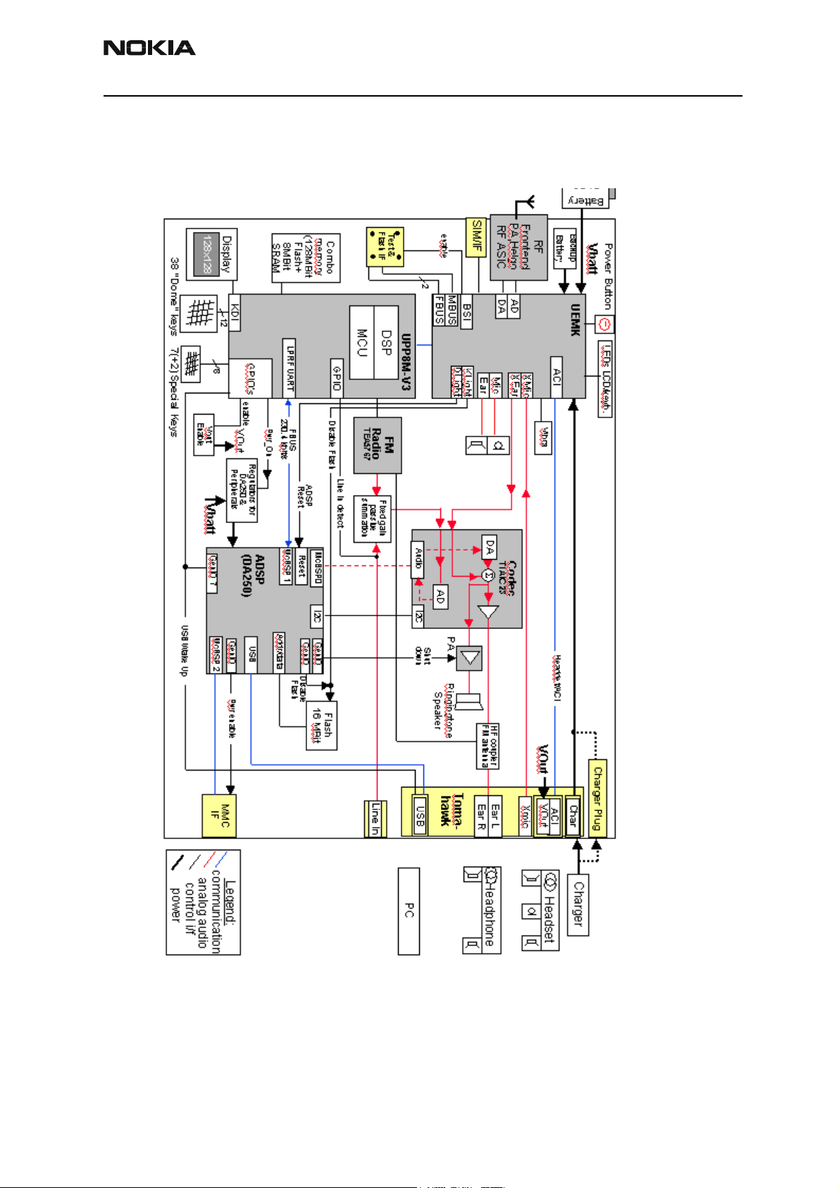
Introduction
Electrical Modules
The NEM-2 phone comprises two modules: the main PWB (EM21) and UI PWB (EM20)
The system module EM11 consists of Radio Frequency (RF) and baseband (BB). User Interface (UI) contains only LCD connector, backlight LEDs, keypad layout and Earpiece circuit.
FM radio is located on the main PWB EM21.
The modules are connected with each other by B2B connectors.
In general NEM-2 baseband hardware consists of two parts:
• GSM Phone
• Audio Player
Phone part is based on DCT4 common baseband architecture. Qwerty-keyboard is connected to UPP ASIC.
Audio Player part contains functionality needed for stereo audio features. MMC interface
and USB interface are included as well.
Phone controls power up and reset of Audio Player part via dedicated hardware signals.
In operational modes both parts are running asynchronous, communication takes place
via UART based asynchronous serial interface.
Special audio routing provides for the connection between audio sources and audio outputs. Audio lines are part of the Phone- Audio Player interface as well.
The purpose of the RF block is to receive and demodulate the radio frequency signal from
the base station and to transmit a modulated RF signal to the base station.
Page 8 Copyright Nokia. All rights reserved. Issue 1 07/03
Page 9
NEM-2
CCS Technical Documentation System Module and User Interface
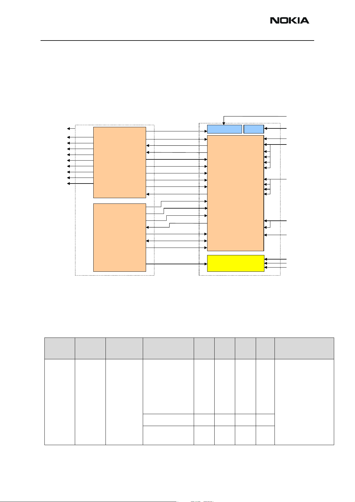
Interconnection Diagram
Figure 1: Interconnection diagram
Issue 1 07/03 Copyright Nokia. All rights reserved.. Page 9
Page 10
NEM-2
System Module and User Interface CCS Technical Documentation
Temperature Conditions
Env. Condition Ambient temperature Note
Normal operation -20°C … +55°C/
-4°F … +131°F
Reduced performance -40°C … -20°C/
-40°F… -4°F and
+55°C … +85°C/
+131°F...+185°F
No operation or storage <-40°C or > +85°C/
<-40°F or > +185°F
Humidity
The modules are not protected against water. Condensated or splashed water might
cause malfunction momentarily. Long term wetness will cause permanent damage.
Absolute Maximum Ratings
Absolute maximum ratings are specified below.
Parameter Min. typ. Max. Unit Note
Battery Voltage
Charger Input Voltage
Specifications fulfilled except FMR is only up to +14°F
For LCD only up to +176°F
No operation or storage. An attempt to operate may damage the phone permanently
–0.3
–0.3
5.5 V
20 V
Page 10 Copyright Nokia. All rights reserved. Issue 1 07/03
Page 11
NEM-2
CCS Technical Documentation System Module and User Interface
DC Characteristics
Main Supply
Signal min. typ. max. Unit Note
VBAT 3.1 3.6 5.1 V
Phone
Signal min. typ. max. Unit Note
BB Regulators
VANA 2.70 2.78 2.86 V I
VFLASH1 2.70 2.78 2.86 V I
VFLASH2 2.70 2.78 2.86 V I
VSIM 1.745
2.91
1.8
3.0
1.855
3.09VV
VIO 1.72 1.8 1.88 V I
VCORE 1.0
1.235
1.425
1.710
1.053
1.3
1.5
1.8
1.106
1.365
1.575
1.890
V
V
V
V
= 80mA
max
= 70mA, I
max
= 40mA
max
I
= 25mA, I
max
= 150mA, I
max
I
= 200mA, I
max
Default value = 1.5V
Signal min. typ. max. Unit Note
VR1A 4.6 4.75 4.9 V
VR1B 4.6 4.75 4.9 V Not used
VR2 2.70
3.20
2.78
3.30
2.86
3.40VV
I
max
= 100mA
sleep
sleep
sleep
sleep
= 2.0mA
= 0.5mA
= 0.5mA
= 0.2mA
VR3 2.70 2.78 2.86 V I
max
= 20mA
VR4 2.70 2.78 2.86 V
VR5 2.70 2.78 2.86 V I
VR6 2.70 2.78 2.86 V I
VR7 2.70 2.78 2.86 V I
= 50mA, I
max
= 50mA, I
max
= 45mA
max
sleep
sleep
= 0.1mA
= 0.1mA
Issue 1 07/03 Copyright Nokia. All rights reserved.. Page 11
Page 12

NEM-2
System Module and User Interface CCS Technical Documentation
Audio Player regulators
Signal min. typ. max. Unit Note
AudioPlayerVcore 1.23
1.42
AudioPlayerVDD 3.23
3.0
AudioPlayerVMMC 3.23
3.0
1.3
1.5
3.3 3.37 V regulated mode;
3.3 3.37 V regulated mode;
1.37
1.58
V default value 1.3V
I
= 300mA
max
unregulated mode;
I
= 300mA
max
unregulated mode;
I
= 60mA
max
Page 12 Copyright Nokia. All rights reserved. Issue 1 07/03
Page 13
NEM-2
CCS Technical Documentation System Module and User Interface
User Interface Modules
Keyboard
NEM-2 features a Qwerty keyboard, two soft keys and send/end keys with additional 4way rocker for gaming and music features. The keys are connected in a 6x7-matrix with
the UPP. Key pressing is detected by scanning procedure.
The applied “Bulls Eye” keypads are located on the UI board.
A “hotkey” for activating the music features and the volume up and down keys are
located on the engine board and connected to GENIO ports.
Display
130*130 pixel passive matrix colour STN display is used.
LCD connector
LCD interface signals are specified below.
No. Symbol Parameter min. typ. max. Unit Note
1 V
2 XRES Reset
3 SDA Serial data Hi: 0.7*V
4 V
5 XCS Chip select
6 SCLK Serial data clock Hi:0.7*V
7 VSS Ground 0 V
8 LED- LED ground 0.505 0.525 0.545 V Connected to
DD
DDI
Voltage supply 2.6 2.75 3.6 V Connected to
VFLASH1 (2.78V)
(active low)
Logic voltage supply
(active low)
Hi:0.7*V
Lo:0
Lo: 0
1.7 1.8 VDD V Connected to
Hi:0.7*V
Lo:0
Lo:0
DDI
DDI
DDI
DDI
Hi: V
DDI
Lo:0.3*V
Hi: V
DDI
Lo: 0.3*V
Hi: V
DDI
Lo:0.3*V
Hi: V
DDI
Lo:0.3*V
V
DDI
V
DDI
VIO (1.8V)
V
DDI
V
DDI
DC-DC converter ‘feedback’
pin
9 NC --- -- -- -- -- Not connected
10 LED+ LED voltage supply 9 10.8 12 V LCD illumination
Issue 1 07/03 Copyright Nokia. All rights reserved.. Page 13
Page 14
NEM-2
System Module and User Interface CCS Technical Documentation
LCD & Keyboard Illumination
For LCD illumination there are 3 white LEDs, which are integrated inside the LCD module.
For driving the LEDs a DC-DC converter is used .
The keypad is illuminated by 4 white LEDs driven also by the DC-DC converter.
UI B2B-Connector
Two UI B2B-connectors are used for connection between engine board and UI board.
No. Symbol Parameter Min. typ. max. Unit Note
1 VIO Supply for LCD 1.72 1.8 1.88 V LCDIF: VDDI (logic supply)
2 VFLASH1 Supply for LCD 2.70 2.78 2.86 V LCDIF: VDD (power supply)
3 GND 0 V
4 GND 0 V
5 LCDUI_0 LCD interface 0 1.8 V LCDIF: SCLK (CLOCK)
6 LCDUI_1 LCD interface 0 1.8 V LCDIF: SDA (SDATA)
7 LCDUI_2 LCD interface 0 1.8 V LCDIF: XCS (Chip select)
8 GENIO_4 LCD interface 0 1.8 V LCDIF: XRES (RESET)
9 GND 0 V
10 GND 0 V
11 LED+ DC-DC con-
verter out
12 LED- DC-DC con-
verter return
13 LED1- Return 1 Return path 1 Keypad illumina-
14 LED2- Return 2 Return path 2 Keypad illumina-
15 Not used
16 Not used
17 GND 0 V
9 10.8 12 V LCD illumination
Open circuit voltage: 20V max
0.525 0.525 0.545 V LCD illumination,
Voltage over feedback resistor
tion
tion
18 GND 0 V
19 GENIO_21 KB i/f 0 1.8 V KEY_BUS12, Column
20 GND V
21 GND V
22 GND V
UI B2B-Connector 1
Page 14 Copyright Nokia. All rights reserved. Issue 1 07/03
Page 15
NEM-2
CCS Technical Documentation System Module and User Interface
No. Symbol Parameter Min. typ. max. Unit Note
1 GND 0 V
2 GND 0 V
3 KEYB_0 Keyboard
Interface
4 KEYB_1 Keyboard
Interface
5 KEYB_2 Keyboard
Interface
6 KEYB_3 Keyboard
Interface
7 KEYB_4 Keyboard
Interface
8 GENIO_2 Keyboard
Interface
9 KEYB_5 Keyboard
Interface
10 KEYB_6 Keyboard
Interface
11 KEYB_7 Keyboard
Interface
12 KEYB_8 Keyboard
Interface
0 1.8 V Column 0= P00 at UPP
0 1.8 V Column 1= P01
0 1.8 V Column 2 = P02
0 1.8 V Column 3 = P03
0 1.8 V Column 4 = P04
0 1.8 V Column 5 = “P05”
0 1.8 V Row 0 = P10
0 1.8 V Row 1 = P11
0 1.8 V Row 2 = P12
0 1.8 V Row 3 = P13
13 KEYB_9 Keyboard
0 1.8 V Row 4 = P14
Interface
14 KEYB_10 Keyboard
0 1.8 V Row 5 = P15
Interface
15 GND 0 V
16 GND 0 V
17 EAR_0 Earpiece
0 2 V
out
18 EAR_0 Earpiece
0 2 V
out
19 EAR_1 Earpiece
0 2 V
out
20 EAR_1 Earpiece
0 2 V
out
21 GND
22 GND
0 V
0 V
PP
PP
PP
PP
Earpiece line 0
Earpiece line 0
Earpiece line 1
Earpiece line 1
Issue 1 07/03 Copyright Nokia. All rights reserved.. Page 15
Page 16
NEM-2
System Module and User Interface CCS Technical Documentation
System Module : Baseband
Baseband Technical Specifications
DC Characteristics
Regulators and Supply Voltage Ranges
Battery Voltage Range
Signal Min. Nom Max Note
VBAT 3.1V 3.6V 4.2V (charging
high limit voltage)
BB Regulators
Signal Min. Nom Max Note
VANA 2.70V 2.78V 2.86V I
VFLASH1 2.70V 2.78V 2.86V I
VFLASH2 2.70V 2.78V 2.86V I
VSIM 1.745V
2.91V
VIO 1.72V 1.8V 1.88V I
VCORE 1.0V
1.235V
1.425V
1.710V
1.8V
3.0V
1.053V
1.3V
1.5V
1.8V
1.855V
3.09V
1.106V
1.365V
1.575V
1.890V
3.1V SW cut off
= 80mA
max
= 70mA
max
= 1.5mA
I
sleep
= 40mA
max
I
= 25mA
max
I
= 0.5mA
sleep
= 150mA
max
= 0.5mA
I
sleep
I
= 200mA
max
I
= 0.2mA
sleep
Default value 1.5V
Accessory Regulator
Signal Min Nom Max Note
Vout 2.72V 2.80 2.88V I
= 70mA
max
RF Regulators
Signal Min Nom Max Note
VR1A 4.6V 4.75V 4.9V I
VR2 2.70V
3.20V
2.78V
3.3V
2.86V
3.40V
max
I
max
= 10mA
= 100mA
Page 16 Copyright Nokia. All rights reserved. Issue 1 07/03
Page 17
NEM-2
A
y
UEMK
CCS Technical Documentation System Module and User Interface
VR3 2.70V 2.78V 2.86V I
VR4 2.70V 2.78V 2.86V I
VR5 2.70V 2.78V 2.86V I
VR6 2.70V 2.78V 2.86V I
VR7 2.70V 2.78V 2.86V I
max
max
I
sleep
max
I
sleep
max
I
sleep
max
= 20mA
= 50mA
= 0.1mA
= 50mA
= 0.1mA
= 50mA
= 0.1mA
= 45mA
Current Sources
Signal Min Nom Max Note
IPA1 and IPA2 0mA - 5mA Programmable, +/-6%
IPA3 and IPA4 50µA 100µA 105µA V
V
IPA1,VIPA1
IPA1
= 0V - 2.7V
= 0V - 2.7V
Power Distribution diagram
Battery
Baseband
VLED+
White LED
Driver
VBAT
VBAT
Audio
Amplifier
UEM
RTC
ccessor
Regulator
RF Regulators
Baseband
Regulators
CHACON
VR1A
VR1B
VR2-7
VSIM
VCORE
VANA
VIO
VFLASH1
VFLASH2
6
SIM
UPP
FLASH
LCD
Backup
battery
FM
Radio
PA Supply
Vout
System Connector
VBAT
IRDA
Issue 1 07/03 Copyright Nokia. All rights reserved.. Page 17
Page 18
NEM-2
System Module and User Interface CCS Technical Documentation
Baseband External and Internal Signals and Connections
This section describes the external and internal electrical connection and interface levels
on the baseband. The electrical interface specifications are collected into tables that
cover a connector or a defined interface.
Figure 2: RF/BB connections block diagram
VR3
VBAT
IPA1
IPA2
VR1A
VR2
VR3
VR4
VR5
VR6
VR7
BB
UEM
UPP
AFCOUT
AUXOUT
RXIINP
RXQINP
TXIOUTP
TXIOUTN
TXQOUTP
TXQOUTN
VrefRF01
PATEMP
GENIO5
GENIO6
GENIO7
RFCLK
RFBUSCLK
RFBUSDA
RFBUSEN1X
GENIO9
VCTCXO VCO
VC
TXC
OUT_BB1_I
OUT_BB1_Q
TXI_0
TXI_180
TXQ_180
TXQ_0
VB_EXT
RFTEMP
TXP
RESET
TXA
REFOUT
SCLK
SDATA
SLE
MODE
MODOUTP_G_TX
MODOUTM_G_TX
MODOUTP_P_TX
MODOUTM_P_TX
Helgo
PA
VCP
VRF_TX
VRF_RX
VF_RX
VLNA
VPAB
VLO
VPRE
VBB
Iref_850
Iref_1800_1900
RF
VR7
VR1A
VR2
VR4
VR5
VR6
VBAT
IPA1
IPA2
Table 1: AC and DC Characteristics of DCT4 RF-Baseband Voltage Supplies
Signal
name
VBAT Battery PA & UEM Voltage 2.95 3.6 4.2 V Battery supply. Cut-
From To Parameter Min Typ Max Unit Function
off level of DCT4 regulators is 3.04V.
Losses in PWB tracks
and ferrites are taken
account to minimum
battery voltage level.
Current 2000 mA
Current drawn by
0.8 2 uA
PA when ”off”
Page 18 Copyright Nokia. All rights reserved. Issue 1 07/03
Page 19
NEM-2
CCS Technical Documentation System Module and User Interface
VR1A UEM HELGO Voltage 4.6 4.75 4.9 V Charge pump output
for SHF VCO tuning.
Current 2 10 mA
Noise density 240 nVr
ms/
sqrt(
Hz)
VR2 UEM HELGO Voltage 2.70 2.78 2.86 V Supply for
I/Q-modulators, buffers, ALS
Current 65 100 mA
Noise density
f=100Hz
f>300Hz
VR3 UEM VCTCXO,
HELGO
VR4 UEM HELGO Voltage 2.70 2.78 2.86 V Supply for Helgo RX;
Voltage 2.70 2.78 2.86 V Supply for VCTCXO,
Current 1 20 mA
Noise density 240 nVr
Current 50 mA
120 nVr
ms/
sqrt(
Hz)
PLL digital parts
ms/
sqrt(
Hz)
PA bias blocks
Noise density decades 20dB/deg from
6Hz to 600 Hz. From
f>600Hz max. noise
density nVrms/
sqrt(Hz)
Noise density
f=6Hz
f=60Hz
f>600Hz
VR5 UEM HELGO Voltage 2.70 2.78 2.86 V Supply for Helgo PLL;
Current 50 mA
Noise density
BW=100Hz...
100kHZ
5500
550
55
240 nVr
nVr
ms/
sqrt(
Hz)
ms/
sqrt(
Hz)
dividers, LObuffers, prescaler,
Issue 1 07/03 Copyright Nokia. All rights reserved.. Page 19
Page 20

NEM-2
System Module and User Interface CCS Technical Documentation
VR6 UEM HELGO Voltage 2.70 2.78 2.86 V Supply for Helgo BB
and LNAs
Current 50 mA
Noise density
BW=100Hz...
100kHz
VR7 UEM SHF VCO Voltage 2.70 2.78 2.86 V Supply for SHF VCO
Current 30 mA
Noise density
100Hz<f<2kHz
2kHz<f<10kHz
10kHz<f<30kHz
30kHz<f<90kHz
90kHz<f<3MHz
VrefRF01 UEM HELGO Voltage 1.334 1.35 1.366 V Voltage Reference for
240 nVr
ms/
sqrt(
Hz)
70
55
35
30
30
nVr
ms/
sqrt(
Hz)
HELGO DCN2
op.amps.
Note: Below 600Hz
noise density is
allowed to increase
20 dB/oct
Current 100 uA
Temp Coef -65 +65 uV/C
Noise density
BW=600Hz...
100kHz
Table 2: AC and DC Characteristics of DCT4 RF-Baseband Digital Signals
Signal name From To Parameter Input Characteristics Function
TXP UPP
(GenIO5)
TXA UPP
(GenIO7)
HELGO ”1” 1.38 1.88 V Power
HELGO ”1” 1.38 1.88 V Power con-
Note
”0” 0 0.4 V
Load Resistance 10 220 kΩ
Load Capacitance 20 pF
Timing Accuracy 1/4 symbol
60 nVr
ms/
sqrt(
Hz)
Min Typ Max Unit
amplifier
enable
trol loop
enable
”0” 0 0.4 V
Page 20 Copyright Nokia. All rights reserved. Issue 1 07/03
Page 21

NEM-2
CCS Technical Documentation System Module and User Interface
Load Resistance 10 220 kΩ
Load Capacitance 20 pF
Timing Accuracy 1/4 symbol
MODE UPP
(GenIO9)
RFBusEn1X UPP HELGO
RFBusDa UPP HELGO
PA ”1” 1.38 1.88 V Power
(SLE)
(SDATA)
amplifier
mode input
”0” 0 0.4 V
Load Resistance 10 220 kΩ
Load Capacitance 20 pF
Timing Accuracy 1/4 symbol
”1” 1.38 1.88 V RFbus ena-
ble
”0” 0 0.4 V
Current 50 uA
Load resistance 10 220 kΩ
Load capacitance 20 pF
”1” 1.38 1.88 V RFbus
data; read/
write
RFBusClk UPP HELGO
(SCLK)
RESET UPP
(GENIO06)
HELGO ”1” 1.38 1.85 V Reset to
”0” 0 0.4 V
Load resistance 10 220 kΩ
Load capacitance 20 pF
Data frequency 10 MHz
”1” 1.38 1.88 V RFBus
clock
”0” 0 0.4 V
Load resistance 10 220 kΩ
Load capacitance 20 pF
Data frequency 10 MHz
Helgo
”0” 0 0.4 V
Load capacitance 20 pF
Load resistance 10 220 kΩ
Timing accuracy 1/4 symbol
Issue 1 07/03 Copyright Nokia. All rights reserved.. Page 21
Page 22

NEM-2
System Module and User Interface CCS Technical Documentation
Table 3: AC and DC Characteristics of DCT4 RF-Baseband Analogue Signals
Signal name From To Parameter Min Typ Max Unit Function
VCTCXO VCTCXO UPP Frequency 13 26 MHz High stability clock
signal for the logic
circuits, AC coupled. Distorted sinewave e.g. sawtooth.
Signal amplitude 0.2 0.8 2.0 Vpp
Input Impedance 10 kΩ
Input Capacitance 10 pF
Harmonic Content -8 dBc
Clear signal window
(no glitch)
Duty Cycle 40 60 %
VCTCXOGnd VCTCXO UPP DC Level 0 V Ground for refer-
RXI/RXQ HELGO UEM Voltage swing
(static)
DC level 1.3 1.35 1.4 V
I/Q amplitude mismatch
I/Q phase mismatch -5 5 deg
TXIP / TXIN UEM HELGO Differential voltage
swing (static)
DC level 1.17 1.20 1.23 V
Source Impedance 200 W
200 mVpp
ence clock
1.35 1.4 1.45 Vpp Received demodulated IQ signals
0.2 dB
2.15 2.2 2.25 Vpp Programmable voltage swing.
Programmable common mode voltage.
Between TXIP-TXIN
TXQP / TXQN UEM HELGO Same spec as for TXIP / TXIN
AFC UEM
(AFCOUT)
TxC UEM
(AUXOUT)
VCTCXO Voltage Min
Max
Resolution 11 bits
Load resistance
and capacitance
Source Impedance 200 W
HELGO Voltage Min
Max
Source Impedance 200 W
0.0
2.4
1
2.4
0.1
2.6
100
0.1 V Transmitter power
V Automatic fre-
quency control signal for VCTCXO
kΩ
nF
level and ramping
control
Page 22 Copyright Nokia. All rights reserved. Issue 1 07/03
Page 23

NEM-2
CCS Technical Documentation System Module and User Interface
Resolution 10 bits
RFTemp HELGO UEM
(PATEMP)
IPA1 / IPA2 UEM PA Output Voltage 0 2.7 V PA final stage quies-
Voltage at -20oC 1,57 V Temperature sensor
of RF.
Voltage at +25oC 1,7
Voltage at +60oC 1,79
cent current adjustment
Current range 0 5 mA
Resolution 4 bits
Current tolerance -6 +6 %
Noise density
f=100 Hz- 800kHz
f=800kHz-100MHz
88
110
nVrms/
sqrt(Hz)
Issue 1 07/03 Copyright Nokia. All rights reserved.. Page 23
Page 24

NEM-2
System Module and User Interface CCS Technical Documentation
FM Radio Interface
BB Signal FM Radio Signal Min Nom Max Condition Note
VFLASH2 Vcca 2.7V 2.78V 2.86V I
Vcc(vco) 2.7V 2.78V 2.86V I
Vccd 2.7V 2.78V 2.86V I
GenIO(3) FMClk 1.4V
0
30ppm Stability
GenIO(8) FMWrEn 1.4V
0V
GenIO(12) FMCtrlDa 1.4V
0
GenIO(11) FMCtrlClk 1.4V
0
FM Antenna RFI1, RFI2 76 MHz 108 MHz FM Input frequency
1.8V 1.88V
0.4V
32kHz Frequency Also 6.5 MHz can be
1.8V 1.88V
0.4V
1.8V 1.88V
0.6V
1.8V 1.88V
0.6V
1 MHz Frequency
High
Low
High
Low
High
Low
High
Low
=10.5 mA
max
=940 µA
max
= 3.9 mA
max
Reference clock for
FM radio module
used
Write/Read enable
Bi-directional data
FM Radio L
FM Radio R
VAFL
VAFR
100mV Audio level
24 dB 30 dB Channel sep-
aration
54dB 60 dB (S+N)/N
2% Harmonic
distortion
Page 24 Copyright Nokia. All rights reserved. Issue 1 07/03
Page 25

NEM-2
CCS Technical Documentation System Module and User Interface
Internal Speaker
Signal Min Nom Max Condition Note
EARP
0.75V 0.8V
EARN
0.75V 0.8V
2.0 V
0.85V
2.0 V
0.85V
pp
AC
DC
pp
AC
DC
Integrated HF Speaker
Signal Min Nom Max Condition Note
IHFP
0.75V 0.8V
IHFN
0.75V 0.8V
2.0 V
0.85V
2.0 V
0.85V
pp
AC
DC
pp
AC
DC
Differential output
(V
= 4.0 Vpp)
diff
Differential output
(V
= 4.0 Vpp)
diff
Issue 1 07/03 Copyright Nokia. All rights reserved.. Page 25
Page 26

NEM-2
System Module and User Interface CCS Technical Documentation
External Signals and Connections
Battery connector
The design is based on “Demi” battery connector.Bottom Connector
No. Symbol Parameter Min. typ. Max. Unit Note
1 VBAT 3.1 3.6 5.1 V Positive battery terminal
2 BSI 68 KOhmBattery capacity measurement
(fixed resistor, connected to GND
inside the battery pack)
3 BTEMP 47 kOhmBattery temperature measure-
ment (measured by NTC
resistor connected to GND inside
pack)
4 GND 0 V Negative/common battery termi-
nal
Bottom connector, or the system connector is of type Pop-Port (TM)
Figure 3: Bottom connector pinout
Contacts, 14 pcs
14
Locking holes for
accessories, 2 pcs
Bottom connector pins and signals:
Page 26 Copyright Nokia. All rights reserved. Issue 1 07/03
Page 27

NEM-2
CCS Technical Documentation System Module and User Interface
No. Symbol
1 Charge V charge 7.0 8.4 9.2 VRMS Fast charger
2 GND Charge GND 0 V Max. serial impedance 100mOhm
3 ACI ACI 1 Kbit/s
4 Vout DC out 2.78 V
5 USB Vbus DC in 4.375 5.25 V USB spec.
6 USB D+ Pos. diff. data 12 Mbit USB spec.
Sig.
Description
min. tip. Max. Unit Note
850 MA
(PWB and connector
850 MA
0 2.78 V Voltage level valid for DCT4
47 Ohm Max. serial impedance for inser-
tion and removal detection
70 MA Max. output current for acc.
0 3.3 V USB spec.
33 Ohm Max. serial impedance
7 USB D- Neg. diff.
data
0 3.3 V USB spec.
8 USB data
GND
9 XMIC N Audio In 300 8k Hz Frequency range 3 dB points
10 XMIC P Audio In 300 8k Hz Frequency range -3 dB points
11 HSEAR N Audio Out 0 V Unbalanced HSEAR design
Data GND 0 V USB spec.
12 Mbit USB spec.
33 Ohm Max. serial impedance
1 Vpp
2.25 V DC voltage
1 Vpp
2.25 V DC voltage
Audio GND Left, decoupling FM
antenna signal
10 Ohm Max. serial impedance
12 HSEAR P Audio Out 30 20k Hz Frequency range -3dB points
with load 32 ohm (headset)
1 V
10 Ohm Max. serial impedance
Issue 1 07/03 Copyright Nokia. All rights reserved.. Page 27
Page 28

NEM-2
System Module and User Interface CCS Technical Documentation
13 HSEAR R NAudio Out 0 V Unbalanced HSEAR design
Audio GND Right, decoupling FM
antenna signal
10 Ohm Max. serial impedance
14 HSEAR R P Audio Out 30 20k Hz Frequency range -3dB points
With load 32 ohm (headset)
1 V
DC Plug
NMP standard 2- or 3-wire chargers are compatible with the Pop-Port connector. The IF
does not support 3-wire charging control.
No. Symbol
B Charge V charge 7.0 8.4 9.2 VRMSFast charger
A GND Charge GND 0 V Max. serial impedance 100mOhm
Signal
Description
min. typ. Max. Unit Note
850 mA
(PWB and connector
850 mA
Audio Line In Connector
Audio line in connector is a 2.5mm stereo jack with internal plug- detection switch .
No. Symbol Parameter min. typ. max. Unit Note
1 GND 0 V
2 Right Level 2 Vrms
3 Impedance 11 13 14.5 kOhm
4 Left Level 2 Vrms
5 Impedance 11 13 14.5 kOhm
6 Detection 0 1.8 V Line in detection
Page 28 Copyright Nokia. All rights reserved. Issue 1 07/03
Page 29

NEM-2
CCS Technical Documentation System Module and User Interface
SIM connector
No. Symbol Parameter min. typ. max. Unit No.
1 SIMCLK Frequency 1.05 3.25 3.36 MHz 1
Trise/Tfall 50 ns
duty cycle 40 60 %
2 SIMRST Voh 0.9 * VSIM VSIM V 2
Vol 0 0.15*VSIM V
3 VSIM 3V SIM Card 2.8 3.0 3.2 V 3
6 mA
1.8V SIM Card 1.6 1.8 2.0
4 GND ground 0 V 4
5 n. c. 5
6 DATA Voh 0.9*VSIM VSIM V 6
Vol 0 0.15*VSIM V
Vih 0.7*VSIM VSIM V
Vil 0 0.15*VSIM V
MMC Connector
NEM-2 supports full size MultiMediaCards with 3.3V power supply
No. Symbol Parameter min. typ. max. Unit Note
1 RSV n. c.
2 CMD Command line -0.5 3.6 V Peak voltage
0.625*VDD VDD+0.3 V Input high voltage
GND-0.3V 0.25*VDD Input low voltage
3 GND -0.5 0 0.5 V
4 VDD 2.0 3.3 3.6 V Supply voltage
5 CLK Clock line -0.5 3.6 V Peak voltage
0 20 MHz Clock frequency
10 ns Clock low/high time
10 ns Clock rise/fall time
6 GND ground -0.5 0 0.5 V
7 DATA 0 Data line 0 -0.5 3.6 V Peak voltage
0.75*VDD V Output high voltage
0.125*VDD V Output low voltage
Issue 1 07/03 Copyright Nokia. All rights reserved.. Page 29
Page 30

NEM-2
System Module and User Interface CCS Technical Documentation
Internal Signals and Connections
Internal microphone
Symbol Parameter Min. typ. max. Unit Note
MICP Differential Input
P
MICN Differential Input
N
MICB Microphone Bias 2.0 2.1 2.25 V DC
200 mVpp 1kOhm to MICB
200 mVpp 1kOhm to GND
Internal speaker
Symbol Parameter Min. typ. max. Unit Note
EARP differential out 2.0 Vpp AC, (Vdiff = 4.0 Vpp)
EARN differential out 2.0 Vpp AC
Vibra
Signal Min. Nom Max Condition Note
VIBRA DC voltage 1.0 1.5 2.3 V Motor average dc
Output
frequency
4 64 512 Hz
Audio player
DA250- SMPS Interface
SMPS (Switch Mode Power Supply) for application DSP core voltage supply needs external clock. ADSP timer 0 provides it. Core voltage level can be changed by VoutSelection
signal, which is connected to ADSP GPIO pin.
Symbol Parameter Min. typ. Max. Unit Note
SMPSClk SMPS synchro-
nization clock
VOutSelection SMPS output
voltage selection
0 3.3 V
460 kHz
0
0.85
0.65
3.3
V low: VCore = 1.5V (default)
high: VCore = 1.3V
Page 30 Copyright Nokia. All rights reserved. Issue 1 07/03
Page 31

NEM-2
CCS Technical Documentation System Module and User Interface
Stereo Codec
Two different interfaces are used between DSP and codec, which runs in master mode:
• I2C control interface
• audio data interface (I2S)
I2C control interface is used for transferring low speed control information between
application DSP and codec. Signal specification of the control interface is given below.
Symbol Parameter Min. typ. Max. Unit Note
SDA serial data 0 3.3 V IIC data line, external 10k pull-
up used
SDL serial clock 0 3.3 V IIC clock line, external 10k pull-
up used
Audio data is transferred via I2S serial digital audio interface. Signal specification of the
audio data interface is listed below.
Symbol Parameter Min. typ. Max. Unit Note
SDATA_IN serial data 0 3.3 V serial data DSP -> codec
SDATA_OUT serial data 0 3.3 V serial data codec -> DSP
LRCIN frame sync. 0 3.3 V frame sync. DSP -> codec
LRCOUT frame sync. 0 3.3 V frame sync. codec -> DSP
BCLK Clock 0 3.3 V clock codec -> DSP
Ringing Tone Speaker Amplifier
Ringing Tone Speaker amplifier shut down pin is connected to ADSP GPIO. Signal specification is given below.
Symbol Parameter Min. typ. Max. Unit Note
APAShutDown shut down 0 3.3 V external pull- down
Issue 1 07/03 Copyright Nokia. All rights reserved.. Page 31
Page 32

NEM-2
System Module and User Interface CCS Technical Documentation
Phone- Audio Player Interface (MADI)
DCT4 Phone- Audio Player interface signals are specified below. Also the nick name
MADI (MCU- ADSP Interface) is frequently used. Refer to section Functional Description
for further details of the DCT4 Phone- Audio Player interface concept.
Symbol Parameter Min. typ. Max. Unit Note
AudioPlayerPwrOn
AudioPlayerResetX
AudioPlayerFlashRPX
AudioPlayerRxD audio player
AudioPlayerTxD audio player
SleepClk RTC clock 0 1.8 V DCT4 Phone -> Audio Player; it is
USBPwrDetection
LineInDetection Line- In detec-
Audio Player
power enable
main Audio
Player reset
Audio Player
flash reset
receive data
transmit data
USB power
detection
tion
0 1.8 V active high; connected to audio
player power supply regulators
0 3.3 V active low; UEMK open drain
output, pull- up resistor inside
Audio Player part
0 3.3 V active low; UEMK open drain
output, pull- up resistor inside
Audio Player part
0 1.8 V DCT4 Phone -> Audio Player; IR
level shifter inside UEMK used
0 3.3 V Audio Player -> DCT4 Phone; IR
level shifter inside UEMK used
under investigation if RTC inside
ADSP is needed
32 kHz
0 1.8 V active high; wake up from sleep
mode
0 1.8 V active high; wake up from sleep
mode
GSM_HF phone audio
out
FM-Radio_R FM radio, right
channel
FM-Radio_L FM radio, left
channel
80 200 mV
80 200 MV
1 Vpp DCT4 Phone -> Audio Player,
mono GSM down link
FMR to Audio Player, stereo
rms
rms
Vrf=1mV, L=R, Delta f=22.5KHz,
fmod=1KHz
FMR to Audio Player, stereo
Vrf=1mV, L=R, Delta f=22.5KHz,
fmod=1KHz
Page 32 Copyright Nokia. All rights reserved. Issue 1 07/03
Page 33

NEM-2
CCS Technical Documentation System Module and User Interface
Baseband Functional Description
Modes of Operation
EM21 baseband has six different functional modes:
• No supply
• Back-up
• Acting Dead
• Active
• Sleep
• Charging
No Supply
In NO_SUPPLY mode, the phone has no supply voltage. This mode is due to disconnection
of main battery and backup battery or low battery voltage level in both of the batteries.
Phone is exiting from NO_SUPPLY mode when sufficient battery voltage level is detected.
Battery voltage can rise either by connecting a new battery with VBAT > V
connecting charger and charging the battery above V
Back-up
In BACK_UP mode the backup battery has sufficient charge but the main battery can be
disconnected or empty (VBAT < V
VRTC regulator is disabled in BACK_UP mode. VRTC output is supplied without regulation
from backup battery (VBACK). All the other regulators are disabled in BACK_UP mode.
Acting Dead
If the phone is off when the charger is connected, the phone is powered on but enters a
state called ”Acting Dead”. To the user, the phone acts as if it was switched off. A battery
charging alert is given and/or a battery charging indication on the display is shown to
acknowledge the user that the battery is being charged.
and VBACK > VBU
MSTR
MSTR+
COFF
or by
MSTR+
.
).
Active
In the Active mode the phone is in normal operation, scanning for channels, listening to
a base station, transmitting and processing information. There are several sub-states in
the active mode depending on if the phone is in burst reception, burst transmission, if
DSP is working etc.
One of the sub-states of the active mode is FM radio on state. In that case, Audio Amplifier and FM radio are powered on. FM radio circuitry is controlled by the MCU and
13MHz-reference clock is generated in the UPP. VFLASH2 regulator is operating.
Issue 1 07/03 Copyright Nokia. All rights reserved.. Page 33
Page 34

NEM-2
System Module and User Interface CCS Technical Documentation
In Active mode the RF regulators are controlled by SW writing into EM’s registers wanted
settings: VR1A can be enabled or disabled. VR2 can be enabled or disabled and its output
voltage can be programmed to be 2.78V or 3.3V. VR4 -VR7 can be enabled, disabled, or
forced into low quiescent current mode. VR3 is always enabled in Active mode.
Sleep Mode
Sleep mode is entered when both MCU and DSP are in stand–by mode. Sleep is controlled by both processors. When SLEEPX low signal is detected UEMK enters SLEEP
mode. VCORE, VIO and VFLASH1 regulators are put into low quiescent current mode. All
the RF regulators are disabled in SLEEP. When SLEEPX=1 detected UEMK enters ACTIVE
mode and all functions are activated.
The sleep mode is exited either by the expiration of a sleep clock counter in the UEMK or
by some external interrupt, generated by a charger connection, key press, headset connection etc.
In sleep mode VCTCXO is shut down and 32 kHz sleep clock oscillator is used as reference
clock for the baseband.
Charging
Charging can be performed in any operating mode.
NEM-2 supports the standard NMP charger interface.
Charging is controlled by the UEMK ASIC and external components are needed for EMC,
reverse polarity and transient protection of the input to the baseband module. The
charger connection is through the system connector interface. The NEM-2 baseband is
designed to support DCT3 chargers from an electrical point of view. Both 2- and 3-wire
type chargers are supported.
The operation of the charging circuit has been specified in such a way as to limit the
power dissipation across the charge switch and to ensure safe operation in all modes.
Battery
780 mAh Li-ion battery pack BLD-3 is used in NEM-2.
Description Value
Nominal discharge cut-off voltage 3.1V
Nominal battery voltage 3.6V
Nominal charging voltage 4.2V
Maximum charger output current 850 mA
Minimum charger output current 200 mA
Page 34 Copyright Nokia. All rights reserved. Issue 1 07/03
Page 35

NEM-2
CCS Technical Documentation System Module and User Interface
Pin numbering of battery pack
Signal name Pin number Function
VBAT 1 Positive battery terminal
BSI 2 Battery capacity measurement (fixed resistor inside the battery
pack)
BTEMP 3 Battery temperature measurement (measured by NTC resistor
inside pack)
GND 4 Negative/common battery terminal
BLD-3 battery pack pin order
Figure 4:
4(GND)
3(BTEMP)
2(BSI)
1 (+)
Issue 1 07/03 Copyright Nokia. All rights reserved.. Page 35
Page 36

NEM-2
System Module and User Interface CCS Technical Documentation
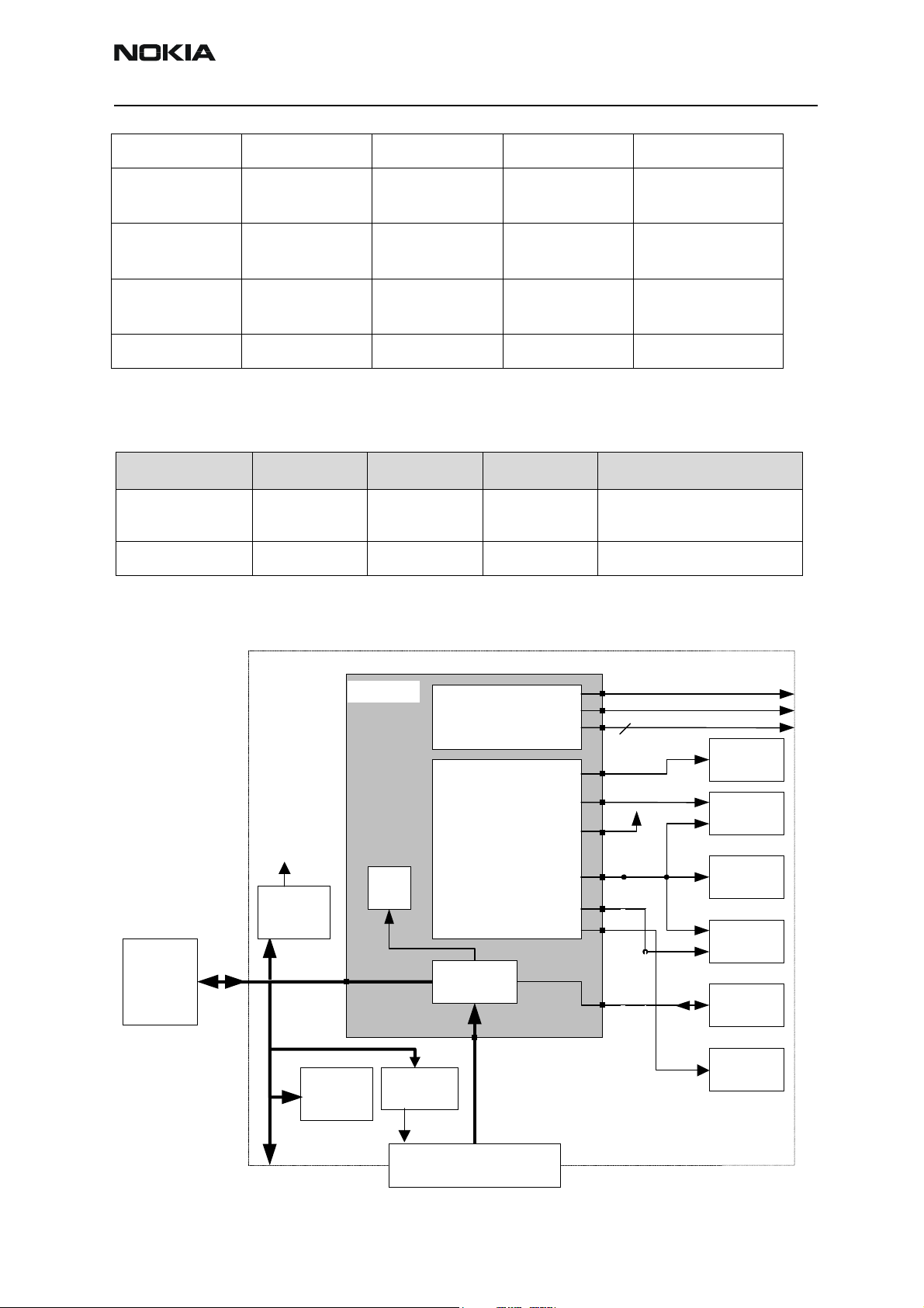
Supply Voltage Distribution
The energy management of NEM-2 is based on DCT4 architecture and additional components for Audio Player power supply. A semi fixed battery supplies the DCT4 Phone part
and the Audio Player part.
UEMK includes several regulators to supply DCT4 Phone RF and baseband. It provides the
energy management including power up and down procedure.
Additional regulators are included for Audio Player supply. These regulators are controlled by UPP GenIO pin.
If the main battery is not present, a backup battery supplies the Real Time Clock (RTC)
part of UEMK. RTC inside ADSP is not supported and powered down permanently.
Figure below shows NEM-2 supply voltage distribution diagram.
Figure 5: NEM-2 Supply Voltage Distribution Diagram
power key
backup
battery
charger
DCT4 Phone Baseband
(UPP, Flash, RF)
GenIO22
Supply (UEM)
RTC
main battery
Audio Player Baseband
(DA250, Flash, codec,
amp., MMC, USB)
Audio Player Power SupplyDCT4 Phone Power
enable
control
power
Page 36 Copyright Nokia. All rights reserved. Issue 1 07/03
Page 37

NEM-2
CCS Technical Documentation System Module and User Interface
Phone
The Phone part supply voltage distribution is controlled by UEMK asic. There are six separate regulators used by baseband. Detailed DCT4 Phone supply voltage distribution diagram is shown in figure below.
Figure 6: Phone Supply Voltage Distribution Diagram
VBAT
passive
LC-
filter
VBACK
UEM
VBATBB1
VBATBB2
VBATBB3
VBATBB4
VBATBB5
VBATVR1
VBATVR2
VBATVR3
VBATVR4
VBATVR5
VBATVR6
VBATVR7
VBATTDriv
VBACK
VDD18
VDD28
VDAAud1
VDAAud2
VDAConvRx
VDAConvTx VRTC
VCORE
VIO
VFLASH1
VFLASH2
VSIM
VR1A
VR1B
VR2
VR3
VR4
VR5
VR6
VR7
VANA
RF
UPP8M
VDDPDRAM
VCORE
VDDMCU
VDDDSP
VDDIO
VDDA
VPP
Flash
VPP
VCC
LCD
VDDI
VDD
FM Radio
VCC
VDIG
SIM
VSIM
Booster
CALLED1
LDO 2.8V
GenIO0
BUZZ0
LEDs
LED+
Tomahawk
Vout
Smart Covers
DC_Out
control
power
Issue 1 07/03 Copyright Nokia. All rights reserved.. Page 37
Page 38

NEM-2
System Module and User Interface CCS Technical Documentation
Audio Player
Audio Player power supply module consist of three different regulators, SMPS type for
DSP core supply with different output voltages, 3.3V LDO type for peripherals and analog
audio supply and 3.3V LDO type for MMC.
Audio Player power supply is controlled by DCT4 Phone part via dedicated hardware signal AudioPlayerPwrEnable. Two supply voltages AudioPlayerVCore and AudioPlayerVDD
are generated inside this block. Refer to chapter Phone- Audio Player Interface (MADI)
for further hardware implementation details.
Audio Player DSP core voltage regulator is dual mode (LDO/ SMPS) type. For SMPS mode
external synchronization frequency is needed. ADSP TOUT0 is used for that purpose. The
ADSP controls AudioPlayerVCore regulator output voltage via GPIO. Therefore ADSP is
able to set his core voltage according to the DSP frequency.
ADSP GPIO controls MMC supply voltage regulator.
AudioPlayerVDD will drop below typical value (3.3V) if battery is discharged. This causes
some audio performance loss. Digital part is not affected by this supply voltage drop.
Detailed Audio Player supply voltage distribution diagram is shown in figure below.
Page 38 Copyright Nokia. All rights reserved. Issue 1 07/03
Page 39

NEM-2
A
A
A
A
A
CCS Technical Documentation System Module and User Interface
Figure 7: Audio Player Supply Voltage Distribution Diagram
VBAT
SMPS
(1.3/ 1.5V)
clock
Vout
AudioPlayerPwrEn
LDO
(3.3V)
AudioPlayerVCore
AudioPlayerVDD
LC- filter
460kHz
Vout selection
udioPlayerVAudio
passive
RC- filter
passive
RC- filter
n. c.
n. c.
DSP DA250
CVDD
RVDD
RCVDD
RDVDD
TOUT0
GPIO2
USBVDD
DVDD
DVDD
VDD
Flash
VPP
VCCQ
VCC
Codec AIC23passive
BVDD
DVDD
VDD
HPVDD
MMCPwrEn
LDO
(3.3V)
APAShutDown
udioPlayerVMMC
AudioPlayerVAPA
passive
LC- filter
Audio Amp
VCC
ShutDown
MMC
VCC
control
power
Issue 1 07/03 Copyright Nokia. All rights reserved.. Page 39
Page 40

NEM-2
A
System Module and User Interface CCS Technical Documentation
Power Up, Power Down and Reset
Phone
Power up, power down and reset of DCT4 Phone part is controlled by the UEMK ASIC.
Audio Player
Audio Player power up, power down and reset is controlled by software via dedicated
hardware signals AudioPlayerPwrEnable, AudioPlayerResetX and AudioPlayerFlashRPX.
Figure below shows the block diagram including Phone reset, Audio Player power control and Audio Player reset signals.
Figure 8: Phone and Audio Player Reset
Audio Player power- up is initialized by activating power enable signal. After power supply settling time Audio Player reset signals can be released.
Clocking
Phone part and Audio Player part uses different oscillators. DCT4 Phone clocking concept
is reused without changes. Two oscillators are implemented:
power key
backup
battery
charger
DCT4 Phone Baseband
(UPP, Flash, RF)
PURX
DCT4 Phone
Power Supply
(UEM)
(UEMK)
main battery
GenIO22
DLight
KLight
Audio Player Baseband
(DA250, Flash, codec,
amp., MMC, USB)
Flash reset
DSP reset
Audio Player Power Supply
enable
control
power
• 32kHz sleep clock
• 26MHz system clock
FMR is connected to UPP FMclk (GENIO3) output pin. FMclk output frequency is set to
32kHz via FM Radio Clock Selection bit in CTSI MCU Clock Control Register 2.
Page 40 Copyright Nokia. All rights reserved. Issue 1 07/03
Page 41

NEM-2
CCS Technical Documentation System Module and User Interface
This clock is distributed to audio codec as well.
Figure 9: Clock Distribution Diagram
32 kHz
UEMK
UEM
VR3
VCTCXO
26MHz
32 kHz
SLEEPX
UPP
MCU
DSP
26 MHz
PLL
CTSI
SLICER
HELGO
HELGO
HELGA
h
26 MHz
RFBUSCLK 13MHz
CBUSCLK 1MHz
DBUSCLK 13MHz
LCDCLK max. 6.5MHz
SIMCLK max. 3.25MHz
Issue 1 07/03 Copyright Nokia. All rights reserved.. Page 41
Page 42

NEM-2
System Module and User Interface CCS Technical Documentation
Phone- Audio Player Interface (MADI)
Phone- Audio Player interface consists of different signals groups:
• power and reset
• wake- up
• communication
•audio
Power and Reset
Three signals are used for Audio Player power supply control and reset:
• AudioPlayerPwrEnable
• AudioPlayerResetX
AudioPlayerPwrEnable controls power supply of Audio Player. It is active high, default
state after reset is low. Phone software can switch Audio Player power supply on by pulling AudioPlayerPwrEnable high.
AudioPlayerResetX controls ADSP reset. It is connected to open drain output Klight of
UEMK asic and ResetX signal of ADSP. External pull-up resistor is used the signal is
active low.
AudioPlayerFlashRPX controls flash reset/ sleep mode input. It is used either for disabling
flash during USB booting or for flash sleep mode control during run time. Therefore it is
connected to open drain output Dlight of UEMK asic, GPIO2 of ADSP and RPX signal of
flash memory. External pull- up resistor is used the signal is active low.
Wake- Up
Transitions from sleep mode into operation mode are triggered by so called wake- up signals. All wake- up signals are connected to UPP. Wake- up signals distributed from Audio
Player part are:
• AudioPlayerFlashRPX
• LineInDetection
• USBWakeUp
LineInDetection is connected to switch inside line- in connector and UPP GenIO13.
Switch is open when line- in plug is inserted. Therefore LineInDetection signal is active
high.
USBWakeUp is connected to Vbus signal of USB connector and UPP GenIO14. LineInDetection signal goes high if USB host is connected and power is supplied on USB Vbus pin.
Therefore USBWakeUp signal is active high.
Page 42 Copyright Nokia. All rights reserved. Issue 1 07/03
Page 43

NEM-2
CCS Technical Documentation System Module and User Interface
Communication interface specified below provides wake- up capability as well. Either
DCT4 Phone or Audio Player will wake- up on activity at the receive lines.
Communication
DCT4 Phone- Audio Player communication interface is serial, UART based asynchronous
interface. Two lines (RxD and TxD) are used. At DCT4 Phone side LPRF UART of UPP is
used. At Audio Player side McBSP0 of DA250 is used.
ADSP internal timer 0 is used for McBSP0 transmit clock. Therefore timer output pin
"TOUT0" is connected to McBSP0 pin "CLKX".
Audio
Two different audio sources are distributed form DCT4 Phone to Audio Player part:
•GSM_HF
• FMRadioOutL, FMRadioOutR
Audio Player
Audio concept is basing on application DSP TMS320DA250. As audio hardware codec
(AD/DA converter) a TLV320AIC23B is used. As FM-radio TEA5767 is used.
The stereo audio hardware codec includes AD- and DA-converter, input amplifier, output
amplifier and headphone amplifier. The headphone amplifier is designed for loads with
resistance greater 16 ohms. The used headset resistance is 32 ohm. The minimal specified
load resistance is 0 ohm in the hardware codec specification. That means that the output
circuit is shortcut protected
Audio Features
Following audio features are supported:
• Telephony in private mode
• Telephony via headset
• Playback from MP3/AAC files via headset
• FM radio via headset
• Recording from analog source via line in or from FM radio in AAC format
• Loading from MP3/AAC files via USB
• Monitoring the recording source via headset
• MP3/AAC ringing tones
Issue 1 07/03 Copyright Nokia. All rights reserved.. Page 43
Page 44

NEM-2
System Module and User Interface CCS Technical Documentation
Audio routing and conditioning
The analog audio sources FM radio and line in are mixed and level conditioned in a passive stereo mixer and then fed through the Audio Codec RLINEIN and LLINEIN. The GSM
downlink from the UEMK HFOUT for headset is added by the codec mono analog input
(MICIN).
Source selection is controlled by software using the mute function for GSM downlink
and power on/off for FM radio. FM radio is powered off when not in use for power saving. The TMUTE pin of the TEA5767 is not used. Disabling the output stage of the UEMK
mutes the GSM downlink signal. Line in signal is the master signal and can’t be muted.
Line in connection is detected via software and switches the FM radio off.
Line in detection is done via sense line from the 2.5mm jack connector to UPP GENIO13.
The amplification and routing of the analog audio sources and outputs of the audio
codec is done via the control interface (SDIN, SCLK, CS, MODE) and the digital audio
interface (LRCIN, DIN, LROUT, DOUT, BCLK) from the DA250.
Audio signal routing is done by software. The hardware concept is fixed wired. The software manages the sources/ inputs and the outputs that will be connected for the used
path. Level and volume control, the equalizing for the selected path and the user wishes
of tone settings or adjustment are also controlled by software. The different use cases
are described in the document Hitchhiker use cases.
When recording from FM radio or line in the signal can be monitored via headset. A
phone call during recording is possible with headset. The recorded signal is mixed into
the GSM downlink by the audio codec with lower level for background monitoring. The
GSM downlink has no influence to the recorded audio signal.
The block diagram of the audio part and the AIC23B audio codec can be found in the following picture.
Page 44 Copyright Nokia. All rights reserved. Issue 1 07/03
Page 45

NEM-2
k
CCS Technical Documentation System Module and User Interface
Figure 10: Audio block diagram
Tomahawk
ACI
XMICP
XMICN
HSEARRP
HSERARN
HSEARLP
HSEARLN
FM-Antenna
UEM HeadInt
UEM Mic2P
UEM Mic2N
Line In
LineIn Detection
UEM HFOUT
DA250
FMradio
LM48 90
DA250
CodecCl
APAShutDown
I2C interface
Issue 1 07/03 Copyright Nokia. All rights reserved.. Page 45
Page 46

NEM-2
System Module and User Interface CCS Technical Documentation
FM Radio
The FM radio in the transceiver NEM-2 is a single chip electronically tuned FM stereo
radio with fully integrated IF selectivity and demodulation. The FM radio is completely
adjustment free.
It can be tuned the European, US and Japanese FM bands.
The channel tuning and bus data are controlled by UPP.
The FM-antenna signal is generated out of the HSEARRN and HSEARN signals from the
bottom connector. FM-radio is only working when headset is connected because the
cable is used as FM-antenna.
SIM Interface
UEMK contains the SIM interface logic level shifting. SIM interface can be programmed
to support 3V and 1.8V SIMs. SIM supply voltage is selected by a register in the UEMK. It
is only allowed to change the SIM supply voltage when the SIM IF is powered down.
The SIM power up/down sequence is generated in the UEMK. This means that the UEMK
generates the RST signal to the SIM. Also the SIMCardDet signal is connected to UEMK.
The card detection is taken from the BSI signal, which detects the removal of the battery.
The SIM interface is powered up when the SIMCardDet signal indicates "card in". This
signal is derived from the BSI signal.
Parameter Variable Min. Typ Max Unit
SIMCARDet, BSI comparator Threshold Vkey 1.94 2.1 2.26 V
SIMCARDet, BSI comparator Hysteresis (1) Vsimhyst 50 75 100 mV
The entire SIM interface locates in two chips: UPP and UEMK.
The SIM interface in the UEMK contains power up/down, port gating, card detect, data
receiving, ATR-counter, registers and level shifting buffers logic. The SIM interface is the
electrical interface between the Subscriber Identity Module Card (SIM Card) and mobile
phone (via UEMK device).
The data communication between the card and the phone is asynchronous half duplex.
The clock supplied to the card is in GSM system 1.083 MHz or 3.25 MHz.
Page 46 Copyright Nokia. All rights reserved. Issue 1 07/03
Page 47

NEM-2
k
k
CCS Technical Documentation System Module and User Interface
Figure 11: SIM interface NEM-2
SIM
C5 C6 C7
C1
C2
C3
C8
C4
From
MultiMediaCard MMC
NEM-2 uses a MMC as memory for the MP3/AAC files. Records from line in or FM radio
can be saved on this card. Also music files via USB can be stored on the MMC. The MMC
can be easy exchanged by the end user and is located under the battery pack. NEM-2 is
supporting MM1 and MM2 standard cards.
SIM
ASIP
SIMIO
SIMCl
SIMRst
VSIM
BSI
UEMK
UEM
SIMIF
register
SIMIO
SIMCl
SIMRst
UEM
digital
logic
UPP
SIMIO
SIMClk
UEMInt
CBusDa
CBusEnX
CBusClk
SIMR
UIF Block
MMC power is supplied by additional discrete 3.3V regulator, which is controlled via
ADSP GPIO.
Flash Memory
ADSP code and data is stored in 16MBit, 16 Mbit wide asynchronous flash memory.
Flash power supply and flash programming supply are connected to AudioPlayerVDD
supply.
Ringing Tone Speaker and Amplifier
A bridge power amplifier (LM4890) drives the ringing tone speaker which can be shutdown via ADSP GPIO6 line. The audio signal is routed from the audio codec (AIC23B)
ROUT and LOUT and is mixed via summation amplifier input to a mono signal.
Audio Digital Signal Processor (ADSP)
SMPS supplies ADSP core hardware modules (AudioPlayerVCore). ADSP peripherals power
supply is connected to AudioPlayerVDD regulator.
Issue 1 07/03 Copyright Nokia. All rights reserved.. Page 47
Page 48

NEM-2
System Module and User Interface CCS Technical Documentation
External Accessory Regulator
An external LDO Regulator exists for accessory power supply purposes. All ACI-accessories require this power supply. Regulator input is connected to battery voltage VBAT and
output is connected to Vout pin in the system connector. Regulator is controlled via UPP
(On/Off-function).
Accessory Regulator Signals
Signal Min. Nom Max Note
Vout 2.70V 2.78 2.86V I
GenIO(0) 1.4 1.8 1.88
0.6
Acoustics
The following chapters give a description of acoustical parts.
Earpiece
Used earpiece is a standard part, NMP code 5140067. Its’ features include impedance
32 ohm, sensitivity 103dB+-3dB dB, SPL/1Vrms input 1kHz.
.
= 150mA
max
High (ON)
Low (OFF)
Figure 12: Earpiece view from top
Page 48 Copyright Nokia. All rights reserved. Issue 1 07/03
Page 49

NEM-2
CCS Technical Documentation System Module and User Interface
Microphone
The microphone is embedded into the B-cover. IT features a sensitivity of 42+/-2dB
(0dB=1V/Pa at 1Khz). Its impedance is 1.4kohm.
Polarity as shown:
Figure 13: Microphone Polarity
Ringing tone speaker
Alerting tones, as MP3, AAC, MIDI or conventional sinusoidal files are made audible by
an integrated loudspeaker. The acoustic pressure level requirement for these ringing
tones is 105dB(A) at a distance of 5cm.
The ringing tone speaker NMP code 5140253, impedance 8 ohm, sensitivity 69B+/-2dB
SPL @ 0.1W, 1m, averaged over rated frequency range.
Polarity as shown:
Pin 1 (+)
Figure 14: Ringing tone speaker Polarity (the view on the spring contacts)
The ringing tone speaker is integrated into the B-cover. An adhesive ring acoustically
seals the lid, which closes the box. The lid is supported with mechanical reinforcements
to stop resonance of the housing. Two cylindrical contact pins, which are moveable
inside the lid, contact the electrical signal through from PWB to the Speaker.
side view
Pin 2 (-)
Vibra
The Vibra code is 6800053.
Issue 1 07/03 Copyright Nokia. All rights reserved.. Page 49
Page 50

NEM-2
System Module and User Interface CCS Technical Documentation
Headset
The headset HDS-3H used is a passive type with stereo headphone and integrated
microphone. It is possible to use a 3rd party stereo headphone with 3.5mm jack plug via
adapter from 3.5mm jack to the Pop-Port plug at the connector. With the same adapter
the output can be used as line out for an external device.
Batteries
Main Battery
780mAh Li-Ion battery pack BLD-3 is used. No other battery packs can be used.
Backup Battery
To preserve the RTC when the main battery is removed, a backup battery is provided.
Polyacene SMD battery type is used. The nominal capacity of the battery is 0.01mAh.
Flash Programming
Flash programming for DCT4 phone part is done in the same way as for all other DCT4
phones. The Audio Player part can be flashed via USB.
For flashing the phone part the same equipment as for all DCT4 phones can be used. Only
for connection of the testpads a special adapter is needed. For USB flashing in field service a special USB cable DKU-2 is needed.
Page 50 Copyright Nokia. All rights reserved. Issue 1 07/03
Page 51

NEM-2
CCS Technical Documentation System Module and User Interface
RF Module Introduction
The RF module performs the necessary high frequency operations of the GSM850/
GSM1900 dualband engine. Both the transmitter and receiver have been implemented by
using direct conversion architecture which means that the modulator and demodulator
operate at the channel frequency.
The core of the RF is an application-specific integrated circuit, Helgo. Another core component is a power amplifier module which includes two amplifier chains, one for
GSM850 and the other for GSM1900.
Other key components include
• 26 MHz VCTCXO for frequency reference
• 3290-3980 MHz SHF VCO (super high frequency voltage controlled oscillator)
• front end module comprising a RX/TX switch and two RF bandpass SAW filters
• TX850 SAW filter and TX1900 Balun
• RX1900 SAW Filter, LNA and RX1900 Balun
The control information for the RF is coming from the baseband section of the engine
through a serial bus, referred later on as RFBus. This serial bus is used to pass the information about the frequency band, mode of operation, and synthesizer channel for the RF.
In addition, exact timing information and receiver gain settings are transferred through
the RFBus. Physically, the bus is located between the baseband ASIC called UPP and
Helgo. Using the information obtained from UPP Helgo controls itself to the required
mode of operation and further sends control signals to the front end and power amplifier
modules. In addition to the RFBus there are still other interface signals for the power
control loop and VCTCXO control and for the modulated waveforms.
RF circuitry is located on one side of the 8 layer PWB.
EMC leakage is prevented by using a metal shield. The RF circuits are separated to three
blocks.
• PA, Antenna Switch module, LNA, 1900 MHz band SAW Filter and 1900 MHz
Balun
• Helgo RF IC and VCTCXO
• VCO and Balun
The RF transmission lines consists of striplines and microstriplines after PA.
Issue 1 07/03 Copyright Nokia. All rights reserved.. Page 51
Page 52

NEM-2
X
System Module and User Interface CCS Technical Documentation
RF Frequency Plan
RF frequency plan is shown below. The VCO operates at the channel frequency multiplied
by two or four depending on the frequency band of operation. This means that the baseband modulated signals are directly converted up to the transmission frequency and the
received RF signals directly down to the baseband frequency.
Figure 15: RF Frequency plan
.
H e l g o
R X 8 5 0 : 8 6 9 - 8 9 4 M H z
R X 1 9 0 0 : 1 9 3 0 - 1 9 9 0 M H z
I - S i g n a l
Q - S i g n a l
R
T X 1 9 0 0 : 1 8 5 0 - 1 9 1 0 M H z
T X 8 5 0 : 8 2 4 - 8 4 9 M H z
f / 4 f / 2
f f
f f
f / 4 f / 2
.
P L L
1 / 1
1 / 2
3 2 9 6 3 9 8 0
M H z
L P F
V C O
2 6 M H z
T C X O
B B C L K
I - S i g n a l
Q - S i g n a l
T X
Page 52 Copyright Nokia. All rights reserved. Issue 1 07/03
Page 53

NEM-2
CCS Technical Documentation System Module and User Interface
DC characteristics
Regulators
The transceiver baseband section has a multi function analog ASIC, UEMK, which contains among other functions six pieces of 2.78 V linear regulators and a 4.8 V switching
regulator. All the regulators can be controlled individually by the 2.78 V logic directly or
through a control register. Normally, direct control is needed because of switching speed
requirement: the regulators are used to enable the RF-functions which means that the
controls must be fast enough.
The use of the regulators can be seen in the power distribution diagram which is presented in Power Distribution Diagram (page 50).
The seven regulators are named VR1 to VR7. VrefRF01(1.35V) is used as Helgo bias reference voltage.
The regulators (except for VR7) are connected to the Helgo. Different modes of operation
can be selected inside the Helgo according to the control information coming through
the RFBus.
List of the needed supply voltages
Volt. source Load
VR1 PLL charge pump (4.8 V)
VR2 TX modulators, ALCs, driver
VR3 VCTCXO, synthesizer digital parts
VR4 Helgo pre-amps, mixers, DtoS
VR5 dividers, LO-buffers, prescaler
VR6 LNAs, Helgo baseband (Vdd_bb)
VR7 VCO
VrefRF01 Helgo Ref. Voltage (DC_Ref)
Vbatt PA
Issue 1 07/03 Copyright Nokia. All rights reserved.. Page 53
Page 54

NEM-2
System Module and User Interface CCS Technical Documentation
Typical current consumption
The table shows the typical current consumption in different operation modes.
Operation mode Current consumption Notes
Power OFF < 10 uA Leakage current (triple band PA)
RX, GSM850 75 mA, peak
RX, GSM1900 70 mA, peak
TX, power level 5, GSM850 1800 mA, peak Efficiency: ca. 45%
TX, power level 0, GSM1900 1100 mA, peak Efficiency: ca. 40%
Page 54 Copyright Nokia. All rights reserved. Issue 1 07/03
Page 55

NEM-2
CCS Technical Documentation System Module and User Interface
RF characteristics
Power Distribution
Figure 16: Power distribution diagram
LNA
GSM1900
Helgo
RX / TX parts
PLL
Issue 1 07/03 Copyright Nokia. All rights reserved.. Page 55
Page 56

NEM-2
System Module and User Interface CCS Technical Documentation
Channel Numbers and Frequencies
System Channel number TX frequency RX frequency Unit
GSM850 128 <= n <=251 F = 824.2 + 0.2 * (n-128) F = 869.2 + 0.2 * (n-128) MHz
GSM1900 512 <= n <= 810 F=1850.2 +0.2*(n-512) F=1930.2+0.2*(n-512) MHz
Main RF characteristics
Parameter Unit and value
Cellular System GSM850, GSM1900
RX Frequency Band GSM850: 869...894 MHz
GSM1900: 1930...1990 MHz
TX Frequency Band GSM850: 824...869 MHz
GSM1900: 1850...1910 MHz
Output Power GSM850: +5...+33 dBm / 3.2 mW... 2 W
Duplex Spacing GSM850: 45MHz
Transmitter characteristics
Item Values (GSM850/GSM1900)
Type Direct conversion, nonlinear, FDMA/TDMA
LO frequency range 3296...3396 MHz / 3700...3820 MHz
Output power 2 W / 1 W peak
Gain control range min. 30 dB
Maximum phase error (RMS/peak) max 5 deg./20 deg. peak
GSM1900: +0...+30 dBm / 1.0 mW... 1 W
GSM1900: 80 MHz
Page 56 Copyright Nokia. All rights reserved. Issue 1 07/03
Page 57

NEM-2
CCS Technical Documentation System Module and User Interface
Receiver characteristics
Item Values, GSM850/GSM1900
Type Direct conversion, Linear, FDMA/TDMA
LO frequencies 3476...3576 MHz / 3860...3980 MHz
Typical 3 dB bandwidth +/- 91 kHz
Sensitivity min. - 102 dBm
Total typical receiver voltage gain (from antenna
to RX ADC)
Receiver output level (RF level -95 dBm) 230 mVpp, single-ended I/Q signals to RX ADCs
Typical AGC dynamic range 83 dB
Accurate AGC control range 60 dB
Typical AGC step in LNA 30 dB GSM1900 / 25 dB GSM850
Usable input dynamic range -102... -10 dBm
RSSI dynamic range -110... -48 dBm
Compensated gain variation in receiving band +/- 1.0 dB
86 dB
RF Block Diagram
The block diagram of the RF module can be seen in Chapter on “RF Block Diagram”. The
detailed functional description is given in the following sections
Issue 1 07/03 Copyright Nokia. All rights reserved.. Page 57
Page 58

NEM-2
GS
850
System Module and User Interface CCS Technical Documentation
RF Block Diagram NEM-2
Figure 17: RF Block Diagram
GSM 850
3290 - 3980 MHz
GSM 1800/1900
M
GSM 1900
HELGO
Page 58 Copyright Nokia. All rights reserved. Issue 1 07/03
Page 59

NEM-2
CCS Technical Documentation System Module and User Interface
Frequency Synthesizers
The VCO frequency is locked by a PLL (phase locked loop) into a stable frequency source
given by a VCTCXO which is running at 26 MHz. The frequency of the VCTCXO is in turn
locked into the frequency of the base station with the help of an AFC voltage which is
generated in UEMK by an 11 bit D/A converter. The PLL is located in Helgo and it is controlled through the RFBus.
The required frequency dividers for modulator and demodulator mixers are integrated in
Helgo.
Loop filter filters out the comparison pulses of the phase detector and generates a DC
control voltage to the VCO. The loop filter determines the step response of the PLL (settling time) and contributes to the stability of the loop.
The frequency synthesizer is integrated in Helgo except for the VCTCXO, VCO, and the
loop filter.
Receiver
Each receiver path is a direct conversion linear receiver. From the antenna the received
RF-signal is fed to a front end module where a diplexer first divides the signal to two
separate paths according to the band of operation: either lower, GSM850 or upper,
GSM1900 path.
Most of the receiver circuitry is included in Helgo.
Transmitter
The transmitter consists of two final frequency IQ-modulators and power amplifiers, for
the lower and upper bands separately, and a power control loop. The IQ-modulators are
integrated in Helgo, as well as the operational amplifiers of the power control loop. The
two power amplifiers are located in a single module and the power detector, directional
coupler, and loop filter parts of the power control loop are implemented as discrete components on the PWB. In the GMSK mode the power is controlled by adjusting the DC bias
levels of the power amplifiers.
Issue 1 07/03 Copyright Nokia. All rights reserved.. Page 59
Page 60

NEM-2
System Module and User Interface CCS Technical Documentation
Front End
The front end features include:
- Antenna 50 ohm input
- RX GSM1900 single output, RX GSM850 balanced output
- TXs single 50 ohm input
-3 control lines from the Helgo
Figure 18: Front End
V _ a n t 1 , 2 , 3
R X
G S M 8 5 0
A n t e n n a
R X
G S M 1 9 0 0
T X
G S M 8 5 0
T X
G S M 1 9 0 0
Page 60 Copyright Nokia. All rights reserved. Issue 1 07/03
Page 61

NEM-2
CCS Technical Documentation System Module and User Interface
Power Amplifier
The power amplifier features include:
- 50 ohm input and output for GSM850/GSM1900
- internal power detector
- Mode: GSM/EDGE
Figure 19: Power amplifier
RF ASIC Helgo
The RF ASIC features include
- Package uBGA108
G S M 8 5 0
o u t
G S M 1 9 0 0
o u t
G S M 8 5 0
P o w e r
C o n t r o l
G S M 1 9 0 0
P o w e r
C o n t r o l
G S M 8 5 0 i n
G S M 1 9 0 0 i n
P o w e r
D e t e c t o r
M o d e
G S M / E D G E
- Balanced I/Q demodulator and balanced I/Q modulator
- Power control operational amplifier, acts as an error amplifier
- The signal from VCO is balanced, frequencies 3290 to 3980 MHz
- GSM850 low noise amplifier (LNA) are integrated.
The Helgo can be tested by test points only.
AFC function
AFC is used to lock the transceiver’s clock to the frequency of the base station.
Antenna
The NEM-2 GSM850/GSM1900 transceiver features an internal antenna.
Issue 1 07/03 Copyright Nokia. All rights reserved.. Page 61
Page 62

NEM-2
System Module and User Interface CCS Technical Documentation
Page 62 Copyright Nokia. All rights reserved. Issue 1 07/03
 Loading...