

Page 1

Programmes After Market Services
COMPACT HANDSFREE
UNIT PHF–3
issue 2 11/97
Page 2

Compact Handsfree Unit PHF–3
After Sales
NHE–8/9
Technical Documentation
COMPACT HANDFREE UNIT PHF–3
Contents
Introduction NO TAG
General NO TAG
Technical Summary NO TAG
Operation NO TAG
List of Modules NO TAG
Basic Specifications NO TAG
Modes of Operation NO TAG
External Signals and Connections NO TAG
Circuit Description NO TAG
Block Diagram NO TAG
Audio Interface Page 7
Power Supply Page 7
Microphone Amplifier Page 7
Xear Amplifier Page 7
Volume Control and Mute Page 7
Speaker Amplifiers Page 7
Charger Page 8
Control Circuit (MCU) Page 8
External I/O and AD–converters Page 8
Connectors Page 8
Input Protection Page 8
Circuit Diagram of DC9 NO TAG
Circuit Diagram of DC9 NO TAG
Layout Diagram of DC9 (version 07) NO TAG
Parts List of DC9 (EDMS Issue 8.2) NO TAG
Exploded View of PHF–3 NO TAG
Assembly Parts NO TAG
Page 2
issue 2 11/97
Page 3

After Sales
Compact Handsfree Unit PHF–3
Technical Documentation
Introduction
General
The PHF–3 is a handsfree unit for handportable (NHE–6 and NHK–6) phones. It
provides rapid charging for the phone and a possibility to use HF–operation. The
PHF–3 cannot be connected directly to the phone but via the external antenna unit
AAH–1D and mobile holder MBT–5 or other devices that provide the HF connector .
Technical Summary
Operation
The PHF–3 has external connections to car battery, ignition sense, car radio
muting, external microphone and external speaker. The unit has a HF–connector
that provides an interface to the phone via external antenna unit. The connection
can be made directly or using the extension cable between PHF–3 and AAH–1D.
There is also an internal speaker inside the handsfree unit.
The unit consists of a switching mode rapid charger, HF–speaker and
HF–microphone amplifiers, volume control circuit, voltage regulators, control
circuit (microprocessor) and a CAP compatible interface.
NHE–8/9
The PHF–3 is always connected to the car battery . To save the car battery , PHF–3
goes in to the sleep mode if the car is not running and/or the phone is not
connected.
List of Modules
Name of Module: Material Code:
HF speaker module DC9 0200656
Assembly parts MPHF–3 0260681
Basic Specifications
Function: Value:
Input voltage 11.3 ... 16 V
Current consumption 2 A dc max
Power source car battery
Page 3
Page 4

Compact Handsfree Unit PHF–3
After Sales
NHE–8/9
Modes of Operation
Phone not connected (sleep mode):
When the phone is not connected the current consumption of the device has been
minimized. The switching mode power supply (SMPS) and audio circuits has been
turned off. PHF–3 is only waiting a phone to be connected.
Phone connected (active mode):
When the phone is connected to the PHF–3 it goes into the active mode. In the
active mode the device provides charging current to the phone via SMPS. It also
can provide hands free call option using the internal or the external speaker (if
connected) and the external microphone. If more private call wants to be made, the
phone itself can be used as a handset without losing the external antenna
connection.
The phone controls all the basic functions of PHF–3 that are required for making
calls. In the active mode the PHF–3 follows the commands received from the phone
via mbus.
PHF–3 also provides car radio mute function during call. This is possible only in
those radios which support that function.
Technical Documentation
PHF–3 can control the mobile antenna motor if it is installed to the car.
External Signals and Connections
D.C. Supply Connector X100
Pin: Signal name: Function:
1, 2 +VB Input from car battery
3 IGNS Ignition sense low
4 CRM Car radio mute off
5 AMC Antenna motor control off
• min/max voltage: 8.0...13.5...16 V dc
• max 1.8 V
Ignition sense high
• min/nom/max 8...13.5...32 V
• nom 0 mA / open collector output
• max 16 V
Car radio mute on
• nom 150 mA / current limiting value
• nom/max 12...15.5 V / at max. current
• nom 0 mA / open collector output
Car radio mute on
• nom 150 mA / current limiting value
• nom/max 12...15.5 V / at max. current
Page 4
6,7,8 GND Ground
issue 2 11/97
Page 5

After Sales
Compact Handsfree Unit PHF–3
Technical Documentation
System Connector X400
Pin Signal name: Function:
1 GND Digital ground
2 XMIC Microphone signal
3 MBUS MBUS line low
4 SGND Signal ground
5 XEAR Speaker signal
6 IGNS Ignition sense
NHE–8/9
• nominal voltage: 60 mVrms
• min/max voltage: 0...0.5 V
MBUS line high
• min/max voltage: 2.4...3.2 V
• typ voltage: 60 mV
• typ voltage: 13.5 V
Pin Signal name: Function:
7,8 +VC Supply voltage
unloaded
limit
9...12 GND Ground
External Microphone Connector X200
Pin: Signal name: Function:
1 GND Ground
2 HFMIC Microphone signal typ voltage: 0 V
External Speaker Connector X300
Pin: Signal name: Notes:
• typ/max voltage: 10.3...10.8 V /
• typ/max current: 780...832 mA / current
Microphone bias typ voltage: 2.5 V dc
1 Speaker – 8 Ω speaker, 3.2 mm jack
2 Speaker +
Page 5
Page 6
Compact Handsfree Unit PHF–3
After Sales
NHE–8/9
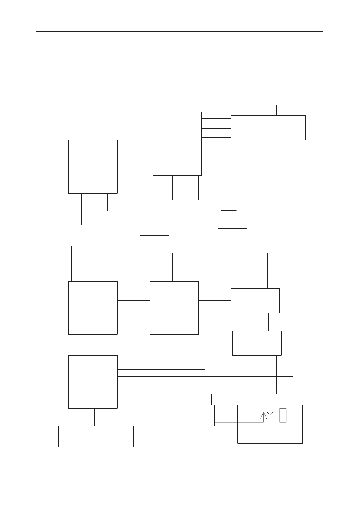
Circuit Description
The circuit blocks are described in the following subsections. Refer to block
diagram in next section. The complexity for each block is given. Note that every
operational amplifier are calculated as a component whereas there actually might
be several amplifiers in one physical (IC) component.
CHARGE
SMPS
CHGON
EXTERNAL
I / O
CRM
AMC
CRM
AMC
IGNS
IGNS
Technical Documentation
VCC
DC connector
X100
VCC
RESET
XEAR
VCHG
System connector
X400
SGND
CAP AUDIO
INTERFACE
MIC
MICROPHONE
AMPLIFIER
CONTROL
MBUS
XMIC
HFEAR EAR
VOL
VOLUME
CONTROL
Attenuation
0 – 28 dB
CIRCUITS
MUTE
ON / OFF
+3V3
PWRON
PRE–
AMPLIFIER
EAR +5V
POWER
AMPLIFIER
SPKR+
POWER
SUPPLY
+5V
V AMP
SPKR–
Page 6
HFMIC
External Microphone
Connector X200
Internal Speaker
Connector X301
External Speaker
Connector X300
issue 2 11/97
Page 7

After Sales
Compact Handsfree Unit PHF–3
Technical Documentation
Audio Interface
This block converts signal levels and also provides single–ended to differential and
level conversions as well as hook pulldown and device identification.
Power Supply
The circuits provides regulated operation voltages to every block. It regulates +3V3
for the operating voltage of MCU, +10V for operating voltage to audio amplifiers,
+5V for bias voltage to audio amplifiers and for the microphone. +2V is for bias
voltage to audio attenuation switches. The power supply voltages has been
designed to achieve maximum ripple voltage rejection.
Microphone Amplifier
This block is a high performance handsfree microphone amplifier . The microphone
and microphone amplifier are biased from the +5V. +10V is used as operating
voltage for the amplifier. The amplifier gain is 30 dB nominal and input impedance
is 2 k. The output AC voltage is about 100 mV. The output impedance is as low
as possible. The circuit performs the sum operation with minimum phase shift. The
amplifier can be muted with the MCU. When microphone is not connected, the input
of the microphone amplifier is grounded.
NHE–8/9
Xear Amplifier
The circuit performs differential to single–ended conversion of incoming audio
signal. The circuit gain is 0 dB. Output DC bias in XEAR line is 1.8 V, input is AC
coupled and the stage tolerates about 1.5 V combined common mode and
differential mode input swing without clipping.
Volume Control and Mute
The circuit is the audio attenuator. Attenuation is performed with operational
amplifiers and audio switches. The circuit performs 8 different audio levels (one is
mute). Attenuation is adjustable with 4 dB steps from 0 dB to 28 dB and mute. MCU
controls attenuation switches with 4 IO–lines, where one of them is the mute.
Speaker Amplifiers
The Preamplifier
The preamplifier is an AC coupled single ended input stage for the power amplifier.
The preamplifier makes most of the XEAR signal amplifying. It uses the +10 V
operating voltage and it is biased to +5 V. Preamplifier has a fixed gain.
Page 7
Page 8

Compact Handsfree Unit PHF–3
After Sales
NHE–8/9
The Power amplifier (PA)
The power amplifier is am AC coupled full bridge output stage with fixed gain. It’s
output impedance is 8 and it is also biased to +5 V. Operating voltage is + 10 V.
The both speaker outputs SP+ and SP– are connected to the internal speaker
connector via the external speaker connector. When the external speaker is
connected, the internal speaker is then muted.
T otal gain for both pre– and power amplifier is about 28 dB. Maximum output power
with the internal speaker is 1.6 W and 3.1 W with the external speaker.
Charger
Charger is the switching mode power supply type. The nominal output voltage of
charger is 10.2 V without load. Limits of the output voltage with all tolerances are
9.3 V to 10.8 V . Nominal output current is 780 mA and limits with tolerance are 714
mA to 832 mA. MCU controls functioning of the charger and checks the output
voltage. Charger is short circuit protected.
Control Circuit (MCU)
Technical Documentation
Micro controller unit (MCU) controls all the functions of the PHF–3. It
communicates with the phone by using the MBUS–line. It has an 8–bit
AD–converter and several IO–lines to control functioning of the other blocks.
External I/O and AD–converters
This block is used to measure specified voltages. It also controls the mobile
antenna motor (AMC) and the car radio mute (CMR). Specified voltages are car
battery voltage +VB, ignition sense voltage (IGNS) and phone charging voltage
+VC. For CRM and AMC current are also controlled by this block.
Connectors
There are 4 external connectors to other units, and one internal speaker connector.
These external connectors are the car connector, the system connector, the
microphone connector and the speaker connector.
Input Protection
The purpose of the input protection is to prevent ESD, RF and high or negative input
voltages to damage the module. Contacts that are subject to ESD are protected
with diode pairs. All inputs are protected from RF.
Page 8
issue 2 11/97
Page 9

After Sales
Compact Handsfree Unit PHF–3
Technical Documentation
Layout Diagram of DC9 (version 08)
NHE–8/9
Page 9
Page 10

Compact Handsfree Unit PHF–3
After Sales
NHE–8/9
Technical Documentation
Parts List of DC9 (EDMS Issue 8.2 Code 0200656)
ITEM CODE DESCRIPTION VALUE TYPE
R101 1430051 Chip resistor 4.7 k 5 % 0.063 W 0603
R102 1415960 Melf resistor 33.2 k 1 % 0.2 W 0204
R103 1414283 Chip resistor 100 k 1 % 0.1 W 0805
R104 1414283 Chip resistor 100 k 1 % 0.1 W 0805
R105 1414283 Chip resistor 100 k 1 % 0.1 W 0805
R106 1414533 Chip resistor 56 k 1 % 0.1 W 0805
R107 1430079 Chip resistor 47 k 5 % 0.063 W 0603
R108 1430079 Chip resistor 47 k 5 % 0.063 W 0603
R109 1430087 Chip resistor 100 k 5 % 0.063 W 0603
R200 1430167 Chip resistor 47 5 % 0.063 W 0603
R201 1430035 Chip resistor 1.0 k 5 % 0.063 W 0603
R202 1430043 Chip resistor 2.2 k 5 % 0.063 W 0603
R203 1430047 Chip resistor 3.3 k 5 % 0.063 W 0603
R204 1430071 Chip resistor 22 k 5 % 0.063 W 0603
R205 1430095 Chip resistor 220 k 5 % 0.063 W 0603
R206 1415939 Melf resistor 22.1 k 1 % 0.2 W 0204
R207 1414283 Chip resistor 100 k 1 % 0.1 W 0805
R208 1415939 Melf resistor 22.1 k 1 % 0.2 W 0204
R209 1415939 Melf resistor 22.1 k 1 % 0.2 W 0204
R210 1415939 Melf resistor 22.1 k 1 % 0.2 W 0204
R211 1430043 Chip resistor 2.2 k 5 % 0.063 W 0603
R300 1430051 Chip resistor 4.7 k 5 % 0.063 W 0603
R301 1415939 Melf resistor 22.1 k 1 % 0.2 W 0204
R302 1415939 Melf resistor 22.1 k 1 % 0.2 W 0204
R304 1415939 Melf resistor 22.1 k 1 % 0.2 W 0204
R305 1430043 Chip resistor 2.2 k 5 % 0.063 W 0603
R306 1414533 Chip resistor 56 k 1 % 0.1 W 0805
R307 1414283 Chip resistor 100 k 1 % 0.1 W 0805
R308 1414283 Chip resistor 100 k 1 % 0.1 W 0805
R309 1430043 Chip resistor 2.2 k 5 % 0.063 W 0603
R310 1414283 Chip resistor 100 k 1 % 0.1 W 0805
R311 1414300 Chip resistor 68 k 1 % 0.1 W 0805
R312 1414452 Chip resistor 10 k 1 % 0.1 W 0805
R313 1414533 Chip resistor 56 k 1 % 0.1 W 0805
R314 1430043 Chip resistor 2.2 k 5 % 0.063 W 0603
R315 1415784 Melf resistor 4.75 k 1 % 0.2 W 0204
R316 1414533 Chip resistor 56 k 1 % 0.1 W 0805
R317 1430043 Chip resistor 2.2 k 5 % 0.063 W 0603
R318 1414276 Chip resistor 47 k 1 % 0.1 W 0805
R319 1414533 Chip resistor 56 k 1 % 0.1 W 0805
R320 1430159 Chip resistor 22 5 % 0.063 W 0603
R321 1415939 Melf resistor 22.1 k 1 % 0.2 W 0204
R322 1415939 Melf resistor 22.1 k 1 % 0.2 W 0204
R323 1430142 Chip resistor 4.7 5 % 0.063 W 0603
Page 10
issue 2 11/97
Page 11

After Sales
Compact Handsfree Unit PHF–3
Technical Documentation
R324 1430142 Chip resistor 4.7 5 % 0.063 W 0603
R325 1415939 Melf resistor 22.1 k 1 % 0.2 W 0204
R401 1430035 Chip resistor 1.0 k 5 % 0.063 W 0603
R402 1430051 Chip resistor 4.7 k 5 % 0.063 W 0603
R403 1430159 Chip resistor 22 5 % 0.063 W 0603
R404 1430159 Chip resistor 22 5 % 0.063 W 0603
R405 1430051 Chip resistor 4.7 k 5 % 0.063 W 0603
R406 1421101 Melf resistor 1.5 1 % 0.2 W 0204
R407 1421101 Melf resistor 1.5 1 % 0.2 W 0204
R408 1421101 Melf resistor 1.5 1 % 0.2 W 0204
R409 1415600 Melf resistor 1.0 k 1 % 0.2 W 0204
R410 1430035 Chip resistor 1.0 k 5 % 0.063 W 0603
R411 1430065 Chip resistor 10 k 5 % 0.063 W 0603
R412 1430065 Chip resistor 10 k 5 % 0.063 W 0603
R413 1421103 Melf resistor 3.16 k 1 % 0.2 W 0204
R414 1430087 Chip resistor 100 k 5 % 0.063 W 0603
R601 1414536 Chip resistor 200 k 1 % 0.1 W 0805
R602 1414276 Chip resistor 47 k 1 % 0.1 W 0805
R603 1430087 Chip resistor 100 k 5 % 0.063 W 0603
R604 1430081 Chip resistor 56 k 5 % 0.063 W 0603
R605 1430087 Chip resistor 100 k 5 % 0.063 W 0603
R606 1430159 Chip resistor 22 5 % 0.063 W 0603
R607 1430087 Chip resistor 100 k 5 % 0.063 W 0603
R608 1430065 Chip resistor 10 k 5 % 0.063 W 0603
R609 1430065 Chip resistor 10 k 5 % 0.063 W 0603
R611 1430065 Chip resistor 10 k 5 % 0.063 W 0603
R612 1430055 Chip resistor 6.8 k 5 % 0.063 W 0603
R613 1414536 Chip resistor 200 k 1 % 0.1 W 0805
R614 1414276 Chip resistor 47 k 1 % 0.1 W 0805
R615 1430035 Chip resistor 1.0 k 5 % 0.063 W 0603
R616 1414536 Chip resistor 200 k 1 % 0.1 W 0805
R617 1414276 Chip resistor 47 k 1 % 0.1 W 0805
R631 1430051 Chip resistor 4.7 k 5 % 0.063 W 0603
R641 1414276 Chip resistor 47 k 1 % 0.1 W 0805
R642 1414536 Chip resistor 200 k 1 % 0.1 W 0805
R643 1430055 Chip resistor 6.8 k 5 % 0.063 W 0603
R801 1430001 Chip resistor 100 5 % 0.063 W 0603
R802 1430001 Chip resistor 100 5 % 0.063 W 0603
R803 1430001 Chip resistor 100 5 % 0.063 W 0603
R806 1430095 Chip resistor 220 k 5 % 0.063 W 0603
C100 2320043 Ceramic cap. 22 p 5 % 50 V 0603
C101 2320063 Ceramic cap. 150 p 5 % 50 V 0603
C102 2517850 Electrol. cap. 220 u 20 % 35 V 10x10
C103 2320063 Ceramic cap. 150 p 5 % 50 V 0603
C104 2320107 Ceramic cap. 10 n 5 % 50 V 0603
C105 2604209 Tantalum cap. 1.0 u 20 % 16 V 3.2x1.6x1.6
C106 2310784 Ceramic cap. 100 n 10 % 25 V 0805
C107 2517850 Electrol. cap. 220 u 20 % 35 V 10x10
NHE–8/9
Page 11
Page 12

Compact Handsfree Unit PHF–3
After Sales
NHE–8/9
C108 2320063 Ceramic cap. 150 p 5 % 50 V 0603
C109 2320091 Ceramic cap. 2.2 n 5 % 50 V 0603
C110 2604209 Tantalum cap. 1.0 u 20 % 16 V 3.2x1.6x1.6
C111 2604209 Tantalum cap. 1.0 u 20 % 16 V 3.2x1.6x1.6
C112 2320091 Ceramic cap. 2.2 n 5 % 50 V 0603
C113 2320091 Ceramic cap. 2.2 n 5 % 50 V 0603
C114 2604209 Tantalum cap. 1.0 u 20 % 16 V 3.2x1.6x1.6
C115 2604209 Tantalum cap. 1.0 u 20 % 16 V 3.2x1.6x1.6
C116 2320107 Ceramic cap. 10 n 5 % 50 V 0603
C117 2604209 Tantalum cap. 1.0 u 20 % 16 V 3.2x1.6x1.6
C118 2604110 Tantalum cap. 10 u 20 % 25 V 7.3x4.4x2.8
C119 2320107 Ceramic cap. 10 n 5 % 50 V 0603
C120 2320091 Ceramic cap. 2.2 n 5 % 50 V 0603
C121 2320063 Ceramic cap. 150 p 5 % 50 V 0603
C200 2320043 Ceramic cap. 22 p 5 % 50 V 0603
C201 2320091 Ceramic cap. 2.2 n 5 % 50 V 0603
C202 2320063 Ceramic cap. 150 p 5 % 50 V 0603
C203 2320063 Ceramic cap. 150 p 5 % 50 V 0603
C204 2320091 Ceramic cap. 2.2 n 5 % 50 V 0603
C205 2320083 Ceramic cap. 1.0 n 5 % 50 V 0603
C206 2310784 Ceramic cap. 100 n 10 % 25 V 0805
C207 2320091 Ceramic cap. 2.2 n 5 % 50 V 0603
C210 2320071 Ceramic cap. 330 p 5 % 50 V 0603
C212 2320063 Ceramic cap. 150 p 5 % 50 V 0603
C213 2320063 Ceramic cap. 150 p 5 % 50 V 0603
C214 2310784 Ceramic cap. 100 n 10 % 25 V 0805
C215 2310784 Ceramic cap. 100 n 10 % 25 V 0805
C216 2320091 Ceramic cap. 2.2 n 5 % 50 V 0603
C218 2310784 Ceramic cap. 100 n 10 % 25 V 0805
C300 2320107 Ceramic cap. 10 n 5 % 50 V 0603
C301 2604209 Tantalum cap. 1.0 u 20 % 16 V 3.2x1.6x1.6
C302 2604209 Tantalum cap. 1.0 u 20 % 16 V 3.2x1.6x1.6
C304 2320083 Ceramic cap. 1.0 n 5 % 50 V 0603
C305 2320083 Ceramic cap. 1.0 n 5 % 50 V 0603
C307 2320083 Ceramic cap. 1.0 n 5 % 50 V 0603
C308 2310784 Ceramic cap. 100 n 10 % 25 V 0805
C309 2320091 Ceramic cap. 2.2 n 5 % 50 V 0603
C312 2320075 Ceramic cap. 470 p 5 % 50 V 0603
C315 2320091 Ceramic cap. 2.2 n 5 % 50 V 0603
C316 2320075 Ceramic cap. 470 p 5 % 50 V 0603
C317 2312292 Ceramic cap. 470 n 20 % Y5 V 1210
C318 2320091 Ceramic cap. 2.2 n 5 % 50 V 0603
C321 2320075 Ceramic cap. 470 p 5 % 50 V 0603
C322 2320083 Ceramic cap. 1.0 n 5 % 50 V 0603
C323 2340014 Ceramic cap. 47 n 10 % 25 V 0805
C324 2604431 Tantalum cap. 10 u 20 % 16 V 6.0x3.2x2.5
C325 2320079 Ceramic cap. 680 p 5 % 50 V 0603
C326 2310784 Ceramic cap. 100 n 10 % 25 V 0805
Technical Documentation
Page 12
issue 2 11/97
Page 13

After Sales
Compact Handsfree Unit PHF–3
Technical Documentation
C327 2320063 Ceramic cap. 150 p 5 % 50 V 0603
C328 2320063 Ceramic cap. 150 p 5 % 50 V 0603
C329 2320063 Ceramic cap. 150 p 5 % 50 V 0603
C330 2320063 Ceramic cap. 150 p 5 % 50 V 0603
C331 2312208 Ceramic cap. 15 n 10 % 50 V 0805
C332 2312208 Ceramic cap. 15 n 10 % 50 V 0805
C333 2320063 Ceramic cap. 150 p 5 % 50 V 0603
C334 2320063 Ceramic cap. 150 p 5 % 50 V 0603
C335 2320043 Ceramic cap. 22 p 5 % 50 V 0603
C336 2320043 Ceramic cap. 22 p 5 % 50 V 0603
C337 2320063 Ceramic cap. 150 p 5 % 50 V 0603
C338 2320063 Ceramic cap. 150 p 5 % 50 V 0603
C339 2320063 Ceramic cap. 150 p 5 % 50 V 0603
C340 2320063 Ceramic cap. 150 p 5 % 50 V 0603
C341 2320063 Ceramic cap. 150 p 5 % 50 V 0603
C342 2320063 Ceramic cap. 150 p 5 % 50 V 0603
C343 2604209 Tantalum cap. 1.0 u 20 % 16 V 3.2x1.6x1.6
C344 2604209 Tantalum cap. 1.0 u 20 % 16 V 3.2x1.6x1.6
C401 2309517 Ceramic cap. 100 n 10 % 50 V 1206
C402 2309517 Ceramic cap. 100 n 10 % 50 V 1206
C403 2309517 Ceramic cap. 100 n 10 % 50 V 1206
C404 2320083 Ceramic cap. 1.0 n 5 % 50 V 0603
C405 2320107 Ceramic cap. 10 n 5 % 50 V 0603
C407 2517850 Electrol. cap. 220 u 20 % 35 V 10x10
C408 2320083 Ceramic cap. 1.0 n 5 % 50 V 0603
C409 2310784 Ceramic cap. 100 n 10 % 25 V 0805
C411 2320083 Ceramic cap. 1.0 n 5 % 50 V 0603
C412 2517850 Electrol. cap. 220 u 20 % 35 V 10x10
C415 2604209 Tantalum cap. 1.0 u 20 % 16 V 3.2x1.6x1.6
C416 2309517 Ceramic cap. 100 n 10 % 50 V 1206
C631 2320059 Ceramic cap. 100 p 5 % 50 V 0603
C632 2320059 Ceramic cap. 100 p 5 % 50 V 0603
C800 2320091 Ceramic cap. 2.2 n 5 % 50 V 0603
C803 2320091 Ceramic cap. 2.2 n 5 % 50 V 0603
C804 2320063 Ceramic cap. 150 p 5 % 50 V 0603
C805 2320083 Ceramic cap. 1.0 n 5 % 50 V 0603
C807 2320063 Ceramic cap. 150 p 5 % 50 V 0603
C808 2320091 Ceramic cap. 2.2 n 5 % 50 V 0603
C809 2320043 Ceramic cap. 22 p 5 % 50 V 0603
C810 2320063 Ceramic cap. 150 p 5 % 50 V 0603
C811 2320091 Ceramic cap. 2.2 n 5 % 50 V 0603
C812 2320043 Ceramic cap. 22 p 5 % 50 V 0603
C813 2320063 Ceramic cap. 150 p 5 % 50 V 0603
C814 2320091 Ceramic cap. 2.2 n 5 % 50 V 0603
C815 2320063 Ceramic cap. 150 p 5 % 50 V 0603
C816 2320091 Ceramic cap. 2.2 n 5 % 50 V 0603
C817 2320063 Ceramic cap. 150 p 5 % 50 V 0603
C818 2320091 Ceramic cap. 2.2 n 5 % 50 V 0603
NHE–8/9
Page 13
Page 14

Compact Handsfree Unit PHF–3
After Sales
NHE–8/9
C819 2320063 Ceramic cap. 150 p 5 % 50 V 0603
C820 2320091 Ceramic cap. 2.2 n 5 % 50 V 0603
C821 2320063 Ceramic cap. 150 p 5 % 50 V 0603
C822 2320110 Ceramic cap. 10 n 10 % 50 V 0603
C823 2320063 Ceramic cap. 150 p 5 % 50 V 0603
C824 2320063 Ceramic cap. 150 p 5 % 50 V 0603
C825 2320063 Ceramic cap. 150 p 5 % 50 V 0603
L100 3641262 Ferrite bead 30r/100mhz 2a 1206 1206
L101 3641262 Ferrite bead 30r/100mhz 2a 1206 1206
L102 3640027 Chip coil 22 u 20 % 0.81 A 6.2x6.6x3
L300 3641262 Ferrite bead 30r/100mhz 2a 1206 1206
L301 3641262 Ferrite bead 30r/100mhz 2a 1206 1206
L400 3641262 Ferrite bead 30r/100mhz 2a 1206 1206
L401 3640039 Chip coil 1.26 A 12x13x6
L800 3641262 Ferrite bead 30r/100mhz 2a 1206 1206
L801 3641262 Ferrite bead 30r/100mhz 2a 1206 1206
L802 3641262 Ferrite bead 30r/100mhz 2a 1206 1206
Z200 3640035 Filt z>450r/100m 0r7max 0.2a 0603 0603
Z600 4507733 Cer.reson 1.0mhz+–0.5% 8.0x5.0smd 8.0x5.0smd
V100 4113933 Trans. supr. 18V 3000 W DO214AB
V101 4200909 Transistor BC858B/BCW30 pnp 30 V 100 mA SOT23
V102 4200917 Transistor BC848B/BCW32 npn 30 V 100 mA SOT23
V400 4215954 MosFet RFD14N05 n–ch 50 V 10 A TO252
V403 4200917 Transistor BC848B/BCW32 npn 30 V 100 mA SOT23
V404 4200909 Transistor BC858B/BCW30 pnp 30 V 100 mA SOT23
V405 4108639 Diode x 2 BAS28 75 V 250 mA SOT143
V406 4108639 Diode x 2 BAS28 75 V 250 mA SOT143
V407 4110074 Schottky diode STPS340U 40 V 3 A SOD6
V408 4110208 Zener diode BZX84 5 % 24 V 0.3 W SOT23
V409 4110150 Zener diode BZX84 2 % 10 V 0.3 W SOT23
V411 4200917 Transistor BC848B/BCW32 npn 30 V 100 mA SOT23
V412 4108639 Diode x 2 BAS28 75 V 250 mA SOT143
V605 4200917 Transistor BC848B/BCW32 npn 30 V 100 mA SOT23
V610 4210020 Transistor BCP69–25 pnp 20 V 1 A SOT223
V611 4200917 Transistor BC848B/BCW32 npn 30 V 100 mA SOT23
V620 4210096 Transistor BCP54 npn 45 V 1.5 A SOT223
V805 4100285 Diode x 2 BAV99 70 V 200 mA SER.SOT23
V806 4100285 Diode x 2 BAV99 70 V 200 mA SER.SOT23
V807 4103003 Diode BRIDGE 600 V 0.5 A MBS
D300 4309488 IC, 4 x bi.switch 74HC4066 SO14S
D600 4370037 IC, MCU uPD78081GB–513 QFP44
N100 4340067 IC, regulator LP2951 3.3 V 100 mA
N101 4340127 Mic29152 reg ld adj 1.5a to263–5 TO263–5
N102 4301199 IC, 2 x op.amp. LM2904 SO8S
N200 4301199 IC, 2 x op.amp. LM2904 SO8S
N300 4301182 IC, 2 x op.amp. LM2902 SO14S
N301 4340125 L2726 2xop.amp pw5w1a 4–28v so20w SO20W
N400 4340067 IC, regulator LP2951 3.3 V 100 mA
Technical Documentation
Page 14
issue 2 11/97
Page 15

After Sales
Compact Handsfree Unit PHF–3
Technical Documentation
N401 4301199 IC, 2 x op.amp. LM2904 SO8S
N402 4305236 IC, 2 x comp. LM2903 SO8S
X100 5416638 Connector 8–pole right angle 1.5 1.5
X200 5200005 Stereo jack + switch 2.5mm. hosid HOSID
X300 5409035 Jack stereo 3.5mm smd SMD
X301 5416640 Pin header m1x2 p1.5 90deg 1a0r02 1A0R02
X400 5440007 12 pins connector for phf–3 and p P
P001 9854136 PC board DC9 54x118x1.6mm d 3/panel
9854136 PCB DC9 54X118X1.6MM D 3/PANEL
NHE–8/9
Page 15
Page 16

Compact Handsfree Unit PHF–3
After Sales
NHE–8/9
Exploded View of PHF–3
1
6
5
Technical Documentation
2
7
4
3
8
10
9
Page 16
issue 2 11/97
Page 17

After Sales
Compact Handsfree Unit PHF–3
Technical Documentation
NHE–8/9
Assembly Parts
ITEM Q’TY CODE DESCRIPTION VALUE, TYPE
1 9450720 Front cover DMD00351
2 5140013 Loudspeaker 1W 15R d64mm h19mm
3 5400994 Connector 2 pole + 2 wire f
4 0200656 HF speaker module DC9
5 9510333 RF shield DMD01230
6 9480290 Acoustic foam DMD01270
7 9780166 Power adapter cable DMJ00016
8 9450719 Back cover DMD00352
9 5 6291928 PT screw KB25X7 WN1412 FeZn blk
10 9380154 Label blank 4D22419 23.8X17.5
Page 17
Page 18

Compact Handsfree Unit PHF–3
After Sales
NHE–8/9
Technical Documentation
This page intentionally left blank.
Page 18
issue 2 11/97
 Loading...