

Page 1

Programmes After Market Services
NHE –8/9 Series Transceivers
Chapter 4
Uif Module
issue 3 12/98
Page 2

NHE –8/9
Uif Module
Technical Documentation
CONTENTS
Introduction 4 – 5. . . . . . . . . . . . . . . . . . . . . . . . . . . . . . . . . . . . . . . . . . . . . . . . . . . . . .
Functional Circuit description 4 – 5. . . . . . . . . . . . . . . . . . . . . . . . . . . . . . . . . . . . . .
Power on/off key 4 – 5. . . . . . . . . . . . . . . . . . . . . . . . . . . . . . . . . . . . . . . . . . . . . .
Keypad switch matrix 4 – 6. . . . . . . . . . . . . . . . . . . . . . . . . . . . . . . . . . . . . . . . . .
Liquid crystal display module 4 – 7. . . . . . . . . . . . . . . . . . . . . . . . . . . . . . . . . . .
Back light 4 – 7. . . . . . . . . . . . . . . . . . . . . . . . . . . . . . . . . . . . . . . . . . . . . . . . . . . .
Keypad back light 4 – 7. . . . . . . . . . . . . . . . . . . . . . . . . . . . . . . . . . . . . . . . . .
LCD back light 4 – 7. . . . . . . . . . . . . . . . . . . . . . . . . . . . . . . . . . . . . . . . . . . . .
Buzzer driver circuitry 4 – 8. . . . . . . . . . . . . . . . . . . . . . . . . . . . . . . . . . . . . . . . . .
Microphone and speaker connection 4 – 8. . . . . . . . . . . . . . . . . . . . . . . . . . . . .
PAMS
Page No
Board to board connection 4 – 8. . . . . . . . . . . . . . . . . . . . . . . . . . . . . . . . . . . . . .
Technical Specifications 4 – 9. . . . . . . . . . . . . . . . . . . . . . . . . . . . . . . . . . . . . . . . . . .
DC Characteristics 4 – 9. . . . . . . . . . . . . . . . . . . . . . . . . . . . . . . . . . . . . . . . . . . .
External Signals and Connections 4 – 9. . . . . . . . . . . . . . . . . . . . . . . . . . . . . . .
Parts List 4–12. . . . . . . . . . . . . . . . . . . . . . . . . . . . . . . . . . . . . . . . . . . . . . . . . . . . . . . .
Uif Module – GU9 _08 4–12. . . . . . . . . . . . . . . . . . . . . . . . . . . . . . . . . . . . . . . . .
Uif Module – GU9_10 4–14. . . . . . . . . . . . . . . . . . . . . . . . . . . . . . . . . . . . . . . . . .
Uif Module – GU9_11 4–16. . . . . . . . . . . . . . . . . . . . . . . . . . . . . . . . . . . . . . . . . .
Page 4 – 2
issue 3 12/98
Page 3

PAMS
NHE –8/9
Technical Documentation
List of Figures
Figure 1. Power Distribution 4 –5. . . . . . . . . . . . . . . . . . . . . . . . . . . . . . . . . . . . . .
Figure 2. Keypad switches – Simplex or Flat–J 4 –6. . . . . . . . . . . . . . . . . . . . .
Figure 3. System board connection pads, order of numbering. 4–10. . . . . . . .
Figure 4. LCD module identification 4–11. . . . . . . . . . . . . . . . . . . . . . . . . . . . . . .
Note: In printed manuals all A3 drawings are located at the back of the binder.
GU9 _08
Figure 5 UIF Schematic 4–A1. . . . . . . . . . . . . . . . . . . . . . . . . . . . . . . . . . . . . . . . . .
Figure 6 UIF Component Layout 4–A2. . . . . . . . . . . . . . . . . . . . . . . . . . . . . . . . . . .
GU9 _10
Figure 7 UIF Component Layout 4–A3. . . . . . . . . . . . . . . . . . . . . . . . . . . . . . . . . . .
Uif Module
Page No
Figure 8 UIF Circuit Diagram 4–A4. . . . . . . . . . . . . . . . . . . . . . . . . . . . . . . . . . . . . . .
GU9 _11
Figure 9 UIF Component Layout 4–A5. . . . . . . . . . . . . . . . . . . . . . . . . . . . . . . . . . .
Figure 10 UIF Circuit Diagram 4–A6. . . . . . . . . . . . . . . . . . . . . . . . . . . . . . . . . . . . .
issue 3 12/98
Page 4 – 3
Page 4

NHE –8/9
Uif Module
PAMS
Technical Documentation
This page intentionally left blank.
Page 4 – 4
issue 3 12/98
Page 5
PAMS
NHE –8/9
Technical Documentation
Introduction
This document describes the User Interface Module GU9.
The GU9 module is intended for use in the GSM and PCN version of the
NHE–8/9 product, that is FLAT–J and Simplex versions.
Functional Circuit description
The following sections of circuitry are included on the PCB:
– Power on/off key.
– Keypad switch matrix.
– Liquid Crystal Display Module and peripheral circuitry
– Keyboard & Display back light circuits
– Buzzer driver circuit and connection pads
– Pads for microphone and speaker connection
– A method of connection between the user interface PCB and the main
system board
Uif Module
The functions are described in details below. See
NO TAG for further information.
VL
VBatt
GND
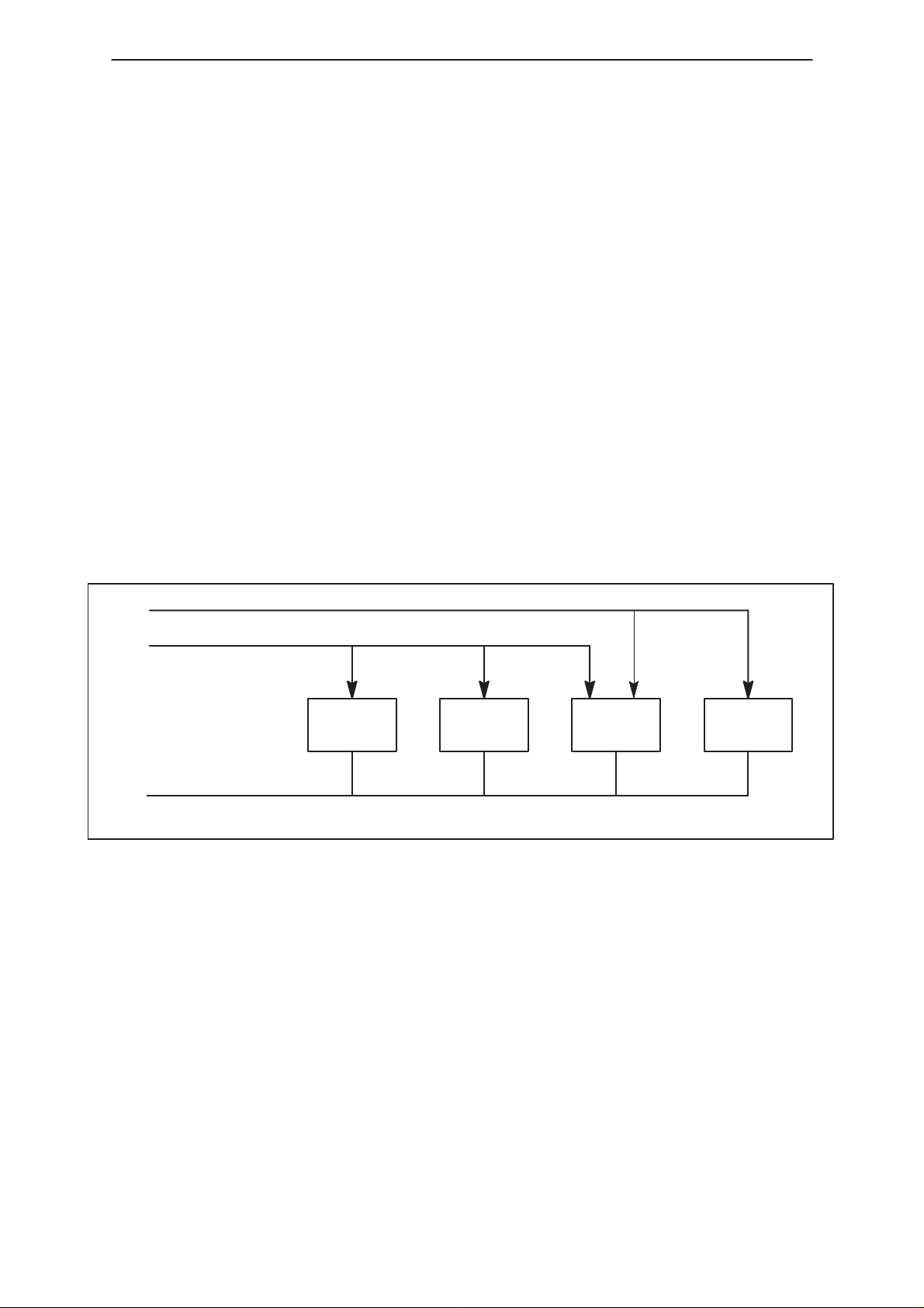
Power on/off key
The power key, S422, is connected directly to the PSCLD via the line
’XPWRON’ and to ’ROW0’ trough the diode V418. When activated both
lines are pulled low.
LCD
Lights
Figure 1. Power Distribution
Key
Lights
UIF Schematic
Buzzer
driver
on page
LCD
When the key is pressed, its row will go low, but the value of the row will
not be changed when the column outputs are set high at the start of the
scanning process. This fact uniquely identifies the key. A diode is
necessary to prevent key presses on any switches connected to ROW0
from turning on/off the phone. This also protect the 3V baseband against
the pull up of XPWRON to VBATT inside PSCLD
The power key,S422, is handled as any other SMD component, and is
placed in the reflow process.
issue 3 12/98
Page 4 – 5
Page 6
NHE –8/9
Uif Module
Keypad switch matrix
The keypad consists of a matrix of 20 switch domes,in the keypad array (0
– 9, #, *, SEND, END, UP, DOWN, CLEAR, ALPHA, SOFTLEFT and
SOFTRIGHT). These are the references on the schematics. The
functionality of the keys are determined via software and is different from
the 3810 version (HD844 MCUSW) and the 3110 version (HD845
MCUSW). The schematics description corresponds to the key pad
functionality in 3810 version.
PAMS
Technical Documentation
X
CLEAR
SOFT
X
UP
X
DOWN
X
123
4
7
*
5
8
0
6
9
#
SOFTLEFT
CLEAR
123
4
7
*
SEND
UP
DOWN
5
8
0
SOFTRIGHT
ALFA
END
6
9
#
3110 Keypad, X: No function
Page 4 – 6
3810 Keypad
Figure 2. Keypad switches
The keypad keys are connected in a 6 by 4 matrix. The 4 outputs
(columns) are normally held at 0V by the ASIC. The 5 rows are also
connected to the ASIC – when any of these inputs goes low (there are
pull–ups inside the ASIC) the ASIC interrupts the MCU, which then
commences scanning. This involves taking all the columns high then
taking each individual column low in turn. When a low is received on a
row input, it can be deduced which key is pressed from the row input
number and the column output which is currently low.
issue 3 12/98
Page 7

PAMS
NHE –8/9
Technical Documentation
ROW5 is also used as an output for the command/data selection on the
LCD driver. A resistor, R406, is necessary to prevent excess current flow
from the row output in case a key is pressed during the time that the LCD
is being accessed.
The keypad consists of gold flashed PCB tracks above which are placed
metal keydomes. The keydomes themselves are supplied attached to a
tape – all the domes in the key array are therefore placed in one
operation.
Liquid crystal display module
The display driver is connected to the system board with a serial data bus.
Data input is enabled when CS1 (LCDENX) is LOW. A0 (ROW5) is
control/display data flag input. Incoming data is control data when A0 is
LOW, and display data when A0 is HIGH. Serial data is read on the rising
edge of SCL. On every eight clock pulse, the data is transferred from the
shift register and processed as 8–bit parallel data. A0 is read on the rising
edge of every eight clock signal.
Uif Module
Back light
LEDs are used as backlights for the keymat and LCD, and are driven by
constant current sources. Constant current sources ensure constant
brightness from the LEDs over the full range of battery voltages (the LEDs
are powered straight from VBatt to lighten the load on the regulated
supply).
Keypad back light
The drive circuits for the keypad LEDs consist of 2 constant current
sources,using two BCX19 transistors wired as simple constant current
sinks. Both transistors supply six LED‘s, so the keyboard is illuminated
with 12 LED‘s. The bases of the two transistor are wired together and
controlled by MCU via the line ’KEYLIGHT’. The led current is fixed by the
values of R401 and R402 and the ratio of R411 to R413.
LCD back light
The display illumination operates in a similar way as the keyboard drivers,
but only one transistor (V402) is used to drive six leds. The current in this
case is defined by the value of R414 and the ratio of R412 to R404. The
constant current source is controlled from an MCU output port via the line
’LCDLIGHT’.
The PCB is gold plated under the LEDs to improve reflection of light
emitted towards the PCB.
issue 3 12/98
Page 4 – 7
Page 8

NHE –8/9
Uif Module
Buzzer driver circuitry
The buzzer is mounted in the A cover, and connected to the UI PCB using
spring contacts mounted on the transducer. When the phone is assembled
the springs press upon pads placed on the UI PCB .
The buzzer is a Citizen CB–09AS–01 device. It is driven from NPN
transistors V403, V425 by a PWM output from the CODEC via the signal
line ’BUZZER’. The ringing volume is controlled by pulse width
modulation.
The diode V413 prevents damage to the transistors when they switch off,
absorbing the stored energy in the buzzer inductance and suppressing
large positive going spikes on the transistor collectors.
The buzzer is driven directly from VBatt in order to have sufficient voltage
to drive sufficient current trough the buzzer.
PAMS
Technical Documentation
Microphone and speaker connection
The microphone and earpiece are mounted in the A cover, and connected
to the UI PCB using spring contacts mounted on the transducers which
press upon pads placed on the UI PCB when the phone is assembled.
The connections are routed directly to the board to board connector pins
19 and 20.
The microphone connections are routed directly to the board to board
connector pins 2 and 3.
EMC filtering is provided using ceramic capacitors.
Board to board connection
A 32 pin spring connector placed on the system board mates with 32 gold
plated pads on the lower side on the UI–PCB. Refer to Table 4 for pin
numbers and signal names.
Page 4 – 8
issue 3 12/98
Page 9

PAMS
50/50
50/50
NHE –8/9
Technical Documentation
Technical Specifications
Table 1. List of Connectors
Connector Name Notes
H400 Display Module Connector FPC footprint for LCD Module
X400 UIF Connector B to B connector . 32 connection pads.
DC Characteristics
Table 2. Supply Voltages
Pin /
Conn.
5 / X400 VL
15 / X400 VBatt
Symbol Minimum Typical /
Nominal
3.0 3.16 3.3 V
5.3 6.0 9.3 V
Maximum Unit Notes
1 mA TBV
Uif Module
200 mA TBV
Table 3. Current consumption @ VBatt
VBatt (V) Keylight (mA) LCDlight (mA) Buzzer
(mAac)
5.3 49.5 22.4 103
6.5 52.4 23.3 123
8.8 58.5 24.9 163
Buzzer current measured with pulse ratio
Notes
External Signals and Connections
Table 4. UI Module Main Connector X400
Pin / Conn. Line Sym-
bol
2 / X400 MICP 0 2 12.5 mVAC Positive Mic terminal
3 / X400 MICN
(AGND)
4,7,11,31/X
400
5 / X400 VL 3.0 3.16 3.3 V Logic voltage
GND 0 V Digital Ground
Minimum Typical /
Nominal
0 2 12.5 mVAC Negative Mic terminal
Maximum Unit Notes
6 / X400 SYSRESET
X
8 / X400 KEYLIGHT
9 / X400 LCDLIGHT
issue 3 12/98
0 0 0.9 V
2.4 3.16 3.3 V
0 0 0.2 V Keymat backlights OFF
2.8 3.16 3.3 V Keymat backlights ON
0 0 0.2 V LCD backlights OFF
2.8 3.16 3.3 V LCD backlights ON
Reset for display driver
Page 4 – 9
Page 10

NHE –8/9
Uif Module
PAMS
Technical Documentation
Table 4. UI Module Main Connector X400 (continued)
Pin / Conn.
bol
10 / X400 BUZZER
12 / X400 GENSCLK
13 / X400 GENSD
14 / X400 LCDENX
15 / X400 VBatt 5.3 6.0 9.3 V Battery voltage
18 / X400 XPWRON
19 / X400 EARN 0 14 220 mVAC Negative Earpiece Ter-
20 / X400 EARP 0 14 220 mVAC Positive Earpiece Ter-
20–25 /
X400
ROW(0:5)
MinimumLine Sym-
Nominal
0 0 0.6 V PWM signal for Buzzer-
LOW
2.4 3.16 3.3 V PWM signal for BuzzerHIGH
0 0 0.6 V Display data clk LOW
2.4 3.16 3.3 V Display data clk HIGH
0 0 0.6 V Display data line LOW
2.4 3.16 3.3 V Display data line HIGH
0 0 0.9 V Display driver Enable
2.4 3.16 3.3 V Display driver Disable
5.3 6.0 9.3 V Power key free, pullup
in PSCLD
0 0.4 V Power key pressed
minal
minal
0 0 0.5 V
2.4 3.16 3.3 V
LCD driving and keyboard ROW reading
NotesUnitMaximumTypical /
26–29 /
X400
COL(0:3)
0 0 0.5 V
2.4 3.16 3.3 V
17
X400
1
Figure 3. System board connection pads, order of numbering.
Column scan for key
matrix
32
16
Page 4 – 10
issue 3 12/98
Page 11

PAMS
NHE –8/9
Technical Documentation
Uif Module
E879 623A0
model name
Figure 4. LCD module identification
Pin 1
Year: 6 : ’96
7: ’97
Product line
Day of week
A : monday
week 23 : week 23
issue 3 12/98
Page 4 – 11
Page 12

NHE –8/9
Uif Module
Technical Documentation
Parts List
Uif Module – GU9 _08
EDMS pn 0200886 Issue 3.6
Item Code Description Value Type
R424 1430015 Chip resistor 470 5 % 0.063 W 0603
R404 1430043 Chip resistor 2.2 k 5 % 0.063 W 0603
R411 1430043 Chip resistor 2.2 k 5 % 0.063 W 0603
R412 1430043 Chip resistor 2.2 k 5 % 0.063 W 0603
R413 1430047 Chip resistor 3.3 k 5 % 0.063 W 0603
R406 1430065 Chip resistor 10 k 5 % 0.063 W 0603
R421 1430065 Chip resistor 10 k 5 % 0.063 W 0603
R425 1430065 Chip resistor 10 k 5 % 0.063 W 0603
R407 1430087 Chip resistor 100 k 5 % 0.063 W 0603
R415 1430111 Chip resistor 1.0 M 5 % 0.063 W 0603
R419 1430131 Chip resistor 464 k 1 % 0.063 W 0603
R401 1430163 Chip resistor 33 5 % 0.063 W 0603
R402 1430163 Chip resistor 33 5 % 0.063 W 0603
R414 1430163 Chip resistor 33 5 % 0.063 W 0603
R416 1430296 Chip resistor 560 k 2 % 0.063 W 0603
C400 2310408 Ceramic cap. Y5 V 1206
C401 2310408 Ceramic cap. Y5 V 1206
C402 2310408 Ceramic cap. Y5 V 1206
C403 2310408 Ceramic cap. Y5 V 1206
C404 2310408 Ceramic cap. Y5 V 1206
C409 2312293 Ceramic cap. Y5 V 1206
C420 2312293 Ceramic cap. Y5 V 1206
C421 2312293 Ceramic cap. Y5 V 1206
C432 2320546 Ceramic cap. 27 p 5 % 50 V 0402
C433 2320546 Ceramic cap. 27 p 5 % 50 V 0402
C410 2320546 Ceramic cap. 27 p 5 % 50 V 0402
C411 2320546 Ceramic cap. 27 p 5 % 50 V 0402
C412 2320546 Ceramic cap. 27 p 5 % 50 V 0402
C413 2320546 Ceramic cap. 27 p 5 % 50 V 0402
C414 2320546 Ceramic cap. 27 p 5 % 50 V 0402
C415 2320546 Ceramic cap. 27 p 5 % 50 V 0402
L401 3645125 Chip coil 12 n 5 % Q=8/100M 0603
L402 3645125 Chip coil 12 n 5 % Q=8/100M 0603
V413 4110070 DiodeBAS16W 75 V 0.25 A SOT323
V418 4110070 DiodeBAS16W 75 V 0.25 A SOT323
V402 4200836 Transistor BCX19 npn 50 V 0.5 A SOT23
V404 4200836 Transistor BCX19 npn 50 V 0.5 A SOT23
V405 4200836 Transistor BCX19 npn 50 V 0.5 A SOT23
PAMS
Page 4 – 12
issue 3 12/98
Page 13

PAMS
NHE –8/9
Technical Documentation
V425 4200836 Transistor BCX19 npn 50 V 0.5 A SOT23
V403 4207461 Transistor BC868–25 npn V SOT89
H400 4850029 LCD display module 83x41+driver+tab+icon
V401 4860005 Led Green 0603
V410 4860005 Led Green 0603
V411 4860005 Led Green 0603
V412 4860005 Led Green 0603
V419 4860005 Led Green 0603
V420 4860005 Led Green 0603
V406 4864389 Led 0603
V408 4864389 Led 0603
V409 4864389 Led 0603
V414 4864389 Led 0603
V416 4864389 Led 0603
V417 4864389 Led 0603
V421 4864389 Led 0603
V422 4864389 Led 0603
V423 4864389 Led 0603
V424 4864389 Led 0603
V427 4864389 Led 0603
V428 4864389 Led 0603
S422 5200120 Push button switch 6.4x5.2 smd
9467014 Lightguide assy dmc00787
9854161 PCB GU9 154.8X135.9X0.8 D 3/PA
Uif Module
issue 3 12/98
Page 4 – 13
Page 14

NHE –8/9
Uif Module
Technical Documentation
Uif Module – GU9_10
EDMS pn 0200886 Issue 3.8
Item Code Description Value Type
R401 1430163 Chip resistor 33 5 % 0.063 W 0603
R402 1430163 Chip resistor 33 5 % 0.063 W 0603
R406 1430047 Chip resistor 3.3 k 5 % 0.063 W 0603
R407 1430087 Chip resistor 100 k 5 % 0.063 W 0603
R411 1430041 Chip resistor 1.8 k 5 % 0.063 W 0603
R412 1430041 Chip resistor 1.8 k 5 % 0.063 W 0603
R413 1430023 Chip resistor 820 5 % 0.063 W 0603
R414 1430163 Chip resistor 33 5 % 0.063 W 0603
R415 1430111 Chip resistor 1.0 M 5 % 0.063 W 0603
R416 1430296 Chip resistor 560 k 2 % 0.063 W 0603
R419 1430131 Chip resistor 464 k 1 % 0.063 W 0603
R425 1430065 Chip resistor 10 k 5 % 0.063 W 0603
C400 2310408 Ceramic cap. Y5 V 1206
C401 2310408 Ceramic cap. Y5 V 1206
C402 2310408 Ceramic cap. Y5 V 1206
C403 2310408 Ceramic cap. Y5 V 1206
C404 2310408 Ceramic cap. Y5 V 1206
C409 2312293 Ceramic cap. Y5 V 1206
C412 2320546 Ceramic cap. 27 p 5 % 50 V 0402
C413 2320546 Ceramic cap. 27 p 5 % 50 V 0402
C414 2320546 Ceramic cap. 27 p 5 % 50 V 0402
C420 2312293 Ceramic cap. Y5 V 1206
C421 2312293 Ceramic cap. Y5 V 1206
H400 4850029 LCD display module
V401 4860005 Led Green 0603
V402 4200836 Transistor BCX19 npn 50 V 0.5 A SOT23
V404 4200836 Transistor BCX19 npn 50 V 0.5 A SOT23
V405 4200836 Transistor BCX19 npn 50 V 0.5 A SOT23
V406 4864389 Led 0603
V408 4864389 Led 0603
V409 4864389 Led 0603
V410 4860005 Led Green 0603
V411 4860005 Led Green 0603
V412 4860005 Led Green 0603
V413 4110070 DiodeBAS16W 75 V 0.25 A SOT323
V414 4864389 Led 0603
V416 4864389 Led 0603
V417 4864389 Led 0603
V418 4110070 DiodeBAS16W 75 V 0.25 A SOT323
PAMS
Page 4 – 14
issue 3 12/98
Page 15

PAMS
NHE –8/9
Technical Documentation
V419 4860005 Led Green 0603
V420 4860005 Led Green 0603
V421 4864389 Led 0603
V422 4864389 Led 0603
V423 4864389 Led 0603
V424 4864389 Led 0603
V425 4200836 Transistor BCX19 npn 50V 0.5A
V427 4864389 Led 0603
V428 4864389 Led 0603
S422 5200120 Push button switch
P001 9854161 PC board
9467014 Lightguide assy
Uif Module
issue 3 12/98
Page 4 – 15
Page 16

NHE –8/9
Uif Module
Technical Documentation
Uif Module – GU9_11
EDMS pn 0200886 Issue 5.0
Item Code Description Value Type
R401 1430163 Chip resistor 33 5 % 0.063 W 0603
R402 1430163 Chip resistor 33 5 % 0.063 W 0603
R406 1430047 Chip resistor 3.3 k 5 % 0.063 W 0603
R407 1430047 Chip resistor 3.3 k 5 % 0.063 W 0603
R411 1430041 Chip resistor 1.8 k 5 % 0.063 W 0603
R412 1430039 Chip resistor 1.5 k 5 % 0.063 W 0603
R413 1430023 Chip resistor 820 5 % 0.063 W 0603
R414 1430163 Chip resistor 33 5 % 0.063 W 0603
R415 1430111 Chip resistor 1.0 M 5 % 0.063 W 0603
R416 1430296 Chip resistor 560 k 2 % 0.063 W 0603
R419 1430131 Chip resistor 464 k 1 % 0.063 W 0603
R425 1430023 Chip resistor 820 5 % 0.063 W 0603
C400 2310408 Ceramic cap. Y5 V 1206
C401 2310408 Ceramic cap. Y5 V 1206
C402 2310408 Ceramic cap. Y5 V 1206
C403 2310408 Ceramic cap. Y5 V 1206
C404 2310408 Ceramic cap. Y5 V 1206
C409 2312293 Ceramic cap. Y5 V 1206
C412 2320546 Ceramic cap. 27 p 5 % 50 V 0402
C413 2320546 Ceramic cap. 27 p 5 % 50 V 0402
C414 2320546 Ceramic cap. 27 p 5 % 50 V 0402
C420 2312293 Ceramic cap. Y5 V 1206
C421 2312293 Ceramic cap. Y5 V 1206
H400 4850029 LCD display module 83x41+driver+tab+icon
V401 4860005 Led Green 0603
V402 4200836 Transistor BCX19 npn 50 V 0.5 A SOT23
V403 4200836 Transistor BCX19 npn 50 V 0.5 A SOT23
V404 4200836 Transistor BCX19 npn 50 V 0.5 A SOT23
V405 4200836 Transistor BCX19 npn 50 V 0.5 A SOT23
V406 4864389 Led 0603
V408 4864389 Led 0603
V409 4864389 Led 0603
V410 4860005 Led Green 0603
V411 4860005 Led Green 0603
V412 4860005 Led Green 0603
V413 4110070 DiodeBAS16W 75 V 0.25 A SOT323
V414 4864389 Led 0603
V416 4864389 Led 0603
V417 4864389 Led 0603
PAMS
Page 4 – 16
issue 3 12/98
Page 17

PAMS
NHE –8/9
Technical Documentation
V418 4110070 DiodeBAS16W 75 V 0.25 A SOT323
V419 4860005 Led Green 0603
V420 4860005 Led Green 0603
V421 4864389 Led 0603
V422 4864389 Led 0603
V423 4864389 Led 0603
V424 4864389 Led 0603
V427 4864389 Led 0603
V428 4864389 Led 0603
S422 5200120 Push button switch 6.4x5.2 smd
P001 9854161 PC board GU9 154.8x135.9x0.8 d 3/pa
9467014 Lightguide assy dmc00787 hd844 HD844
Uif Module
issue 3 12/98
Page 4 – 17
Page 18

NHE –8/9
Uif Module
PAMS
Technical Documentation
This page intentionally left blank.
Page 4 – 18
issue 3 12/98
 Loading...