

Page 1

Nokia Customer Care
7-System Module
ISSUE 1 09/2004 Copyright ©2004 Nokia Corporation. All Rights Reserved
Page 2

RH-59/60
Nokia Customer Care 7-System Module
[This page left intentionally blank]
2 COMPANY CONFIDENTIAL ISSUE 1 09/2004
Copyright © 2004 Nokia. All Rights Reserved.
Page 3

RH-59/60
7-System Module Nokia Customer Care
Table of Contents
Page No
RH-59/60, Nokia 2600..........................................................................................9
Baseband HW iIntroduction.............................................................................. 9
Technical summary............................................................................................ 9
Modes of operation. ......................................................................................... 10
No supply .......................................................................................................10
Power_off .......................................................................................................11
Acting dead ....................................................................................................11
Active .............................................................................................................11
Sleep mode ....................................................................................................11
Charging ........................................................................................................11
DC characteristics............................................................................................ 13
Supply voltage ranges ................................................................................... 13
Interconnection diagram .................................................................................. 14
External signals and connections .................................................................... 14
System connector (X102) ..............................................................................14
Battery connector ...........................................................................................16
Baseband – RF interface ............................................................................... 17
Internal signals and connections...................................................................... 17
Audio ..............................................................................................................17
Baseband board clocks ..................................................................................18
Functional Description ..................................................................................... 19
Audio external.................................................................................................. 19
Audio internal .................................................................................................19
Earpiece .........................................................................................................19
Microphone ....................................................................................................20
Batteries........................................................................................................... 21
Keyboard............................................................................................................ 22
Memory module............................................................................................... 23
SIM interface.................................................................................................... 23
Vibra ...............................................................................................................23
Test interfaces ................................................................................................. 24
Connections to baseband................................................................................ 24
FBUS interface ...............................................................................................24
MBUS interface .............................................................................................. 24
General Description of the RF circuits............................................................ 25
Receiver signal path ........................................................................................ 25
Transmitter signal path .................................................................................... 26
PLL................................................................................................................... 26
Power supply ................................................................................................... 28
ISSUE 1 09/2004 COMPANY CONFIDENTIAL 3
Copyright © 2004 Nokia. All Rights Reserved.
Page 4

RH-59/60
Nokia Customer Care 7-System Module
List of Figures
Page No
Fig 1 Baseband block diagram.............................................................................. 9
Fig 2 Power distribution diagram........................................................................... 14
Fig 3 Headset Interface......................................................................................... 19
Fig 4 Earpiece interface ........................................................................................ 20
Fig 5 Bottom connector including the microphone................................................ 20
Fig 6 Internal electrical microphone interface ....................................................... 21
Fig 7 BL-5C Battery.............................................................................................. 21
Fig 8 SIM interface................................................................................................23
Fig 9 Vibra driver circuit ........................................................................................23
Fig 10 Receiver signal path.................................................................................. 25
Fig 11 Transmitter signal path............................................................................... 26
Fig 12 Power supply configuration.......................................................................28
4 COMPANY CONFIDENTIAL ISSUE 1 09/2004
Copyright © 2004 Nokia. All Rights Reserved.
Page 5

RH-59/60
7-System Module Nokia Customer Care
[This page left intentionally blank]
ISSUE 1 09/2004 COMPANY CONFIDENTIAL 5
Copyright © 2004 Nokia. All Rights Reserved.
Page 6
RH-59/60
Nokia Customer Care 7-System Module
Abbreviations
Abbr.
Description
ACI Accessory Control Interface
ADC Analog Digital Connector
ARM Advanced RISC Machines
ASIC Application Specific Integrated Circuit
ATR Answer To Reset
BB Baseband
BL-5C Battery type.
BSI Battery Size Indicator
Cbus Control bus (internal phone interface between UPP-UEM)
CCS Customer Care Service
CPH Copenhagen, Denmark
CTI Cover Type Indicator
CTSI Clock Timing Sleep and Interrupt
Dbus DSP controlled bus (Internal phone interface between UPP-UEM)
DC Direct Current
DCT4.0 Digital Core Technology, generation 4.0
DSP Digital Signal Processor
DUT Device under test
EAD External Accessory Detection
EMC Electro Magnetic Compatibility
ESD Electro Static Discharge
Fbus Fast Bus, asynchronous message bus connected to DSP (communica-
tions bus)
FCI Functional cover interface
FPC Flexible printed circuit
FR Full Rate
GENIO General Purpose Input/Output
GSM Global System Mobile
HW Hardware
6 COMPANY CONFIDENTIAL ISSUE 1 09/2004
Copyright © 2004 Nokia. All Rights Reserved.
Page 7
RH-59/60
7-System Module Nokia Customer Care
IF Interface
IHF Integrated Hands Free
IMEI International Mobile Equipment Identity
LCD Liquid Crystal Display
LDO Low Drop Out
LED Light Emitting Diode
Li-Ion Lithium Ion battery
Lion Battery program
LN Lotus Notes
LPRF Low Power Radio Frequency
MALT Medium And Loud Transducer
Mbus Asynchronous message bus connected to MCU (phone control interface).
Slow message bus for control data.
MCU Micro Controller Unit
NO_SUPPLY UEM state where UEM has no supply what so ever
NRT Nokia Ringing Tones
NTC Negative temperature Coefficient, temperature sensitive resistor used as
a temperature sensor.
PA Power Amplifier (RF)
PDA Personal Digital Assistant
PDM Pulse Density Modulation
PDRAM Program/Data RAM
Phoenix SW tool of DCT4.x
PLL Phase locked loop
PnPHF Plug and Play Handsfree
PUP General Purpose IO (PIO), USARTS and Pulse Width Modulators
PWB Printed Wired Board
PWR_OFF UEM state where phone is off
PWRONX Signal from power on key.
R&D Research and development
RESET UEM state where regulators are enabled
RTC UEM internal Real Time Clock
ISSUE 1 09/2004 COMPANY CONFIDENTIAL 7
Copyright © 2004 Nokia. All Rights Reserved.
Page 8
RH-59/60
Nokia Customer Care 7-System Module
SARAM Single Access RAM
SIM Subscriber Identification Module
SLEEP UEM power saving state controlled by UPP
SPR Standard Product Requirements
SRAM Static RAM
STI Serial Trace Interface
SW Software
TBSF Through the Board Side Firing
TDB To Be Defined
TI Texas Instruments
UEM Universal Energy Management
UI User Interface
UPP Universal Phone Processor
VBAT Main battery voltage
VCHAR Charger input voltage
VCHARDET Charger detection threshold level
VMSTR+, VM-
STR
Master Reset threshold level
8 COMPANY CONFIDENTIAL ISSUE 1 09/2004
Copyright © 2004 Nokia. All Rights Reserved.
Page 9
RH-59/60
7-System Module Nokia Customer Care
RH-59/60, Nokia 2600
■ Baseband HW iIntroduction
This document specifies the baseband module for the Nokia 2600. The baseband module includes the baseband engine chipset, the UI components and the acoustical p arts for the transceiver.
Nokia 2600 is a hand-portable dualband 900/1800MHz or Low band/High ba nd phon e, featuring the DCT4 generation baseband (UEM/UPP) and RF (MJOELNER) circuitry.
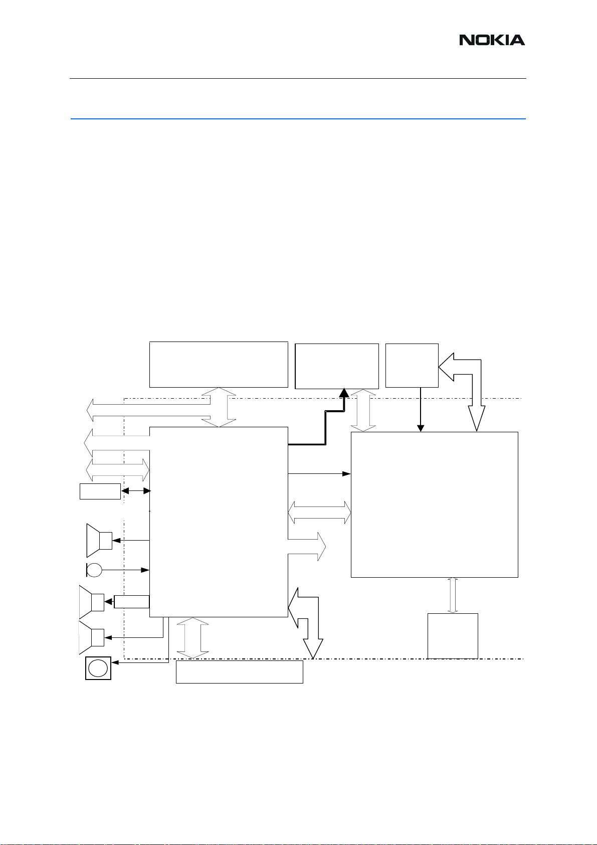
■ Technical summary
The baseband module contains 2 main ASICs named the UEM and UPP. The baseband module furthermore contains a Flash IC of 32Mbit. The baseband is based on the DCT4 engine program.
Figure 1:Baseband block diagram
PA Supply
RF Supplies
RF RX/TX
SIM
Flashlight
EAR
MIC
speaker
Buzzer
IHF
UI
Battery
Baseband
UEM
External Audio
Charger connection
DLIGHT
SLEEPCLK
32kHz
CBUS/
DBUS
BB
Supplies
Mjoelner
26MHz
UPP
RFBUS
FLASH
MEMADDA
M
VIBRA
DCT4 Janette connector
DCT4 connector
MBus/FBus
The UEM supplies both the baseband module as well as the RF module with a series of voltage
regulators. Both the RF and Baseband modules are supplied with regulated voltages of 2.78 V
and 1.8V. UEM includes 6 linear LDO (low drop-out) regulators for baseband and 7 regulators
ISSUE 1 09/2004 COMPANY CONFIDENTIAL 9
Copyright © 2004 Nokia. All Rights Reserved.
Page 10

RH-59/60
Nokia Customer Care 7-System Module
for RF. The UEM is furthermore supplying the baseband SIM interface with a programmable
voltage of either 1.8 V or 3.0 V. The core of the UPP is supplied with a programmable voltage
of 1.0 V, 1.3 V, 1.5 V or 1.8 V.
UPP operates from a 26MHz clock, coming from the RF ASIC MJOELNER, the 26 MHz clock
is internally divided by two, to the nominal system clock of 13MHz. DSP and MCU contain
phase locked loop (PLL) clock multipliers, which can multiply the system.
The UEM contains a real-time clock, sliced down from the 32768 Hz crystal oscillator. The
32768 Hz clock is fed to the UPP as a sleep clock.
The communication between the UEM and the UPP is done via the bi-directional serial busses
CBUS and DBUS. The CBUS is controlled by the MCU and operates at a speed of 1 MHz set
by SW. The DBUS is controlled by the DSP and operates at a speed of 13 MHz. Both processors are located in the UPP.
The UEM ASIC mainly handles the interface between the baseband and the RF section. UEM
provides A/D and D/A conversion of the in-phase and quadrature receive and transmit signal
paths and also A/D and D/A conversions of received and transmitted audio signals to and from
the user interface. The UEM supplies the analog signals to RF section according to the UPP
DSP digital control.
RF ASIC MJOELNER is controlled through UPP RFBUS serial interface. There are also separate signals for PDM coded audio. Digital speech processing is handled by the DSP inside UPP
ASIC. UEM is a dual voltage circuit, the digital parts are running from the baseband sup ply 1.8V
and the analog parts are running from the analog supply 2.78V, also VBAT is directly used by
some blocks.
The baseband supports both internal and external microphone inputs and speaker outputs.
The transceiver module is implemented on 6 layer selective OSP/Gold coated PWB.
■ Modes of operation
baseband has six different operating modes (in normal mode):
•No_Supply
•Power_off
•Acting_Dead
•Active
•Sleep
•Charging
Additionally two modes exist for product verification: 'testmode' and 'local mode'.
No supply
In No_Supply mode, the phone has no supply voltage. This mode is due to disconnection of
main battery or low battery voltage level.
Phone is exiting from No_Supply mode when sufficient battery vo ltage level is detected. Battery
voltage can rise either by connecting a new battery with VBA T > V
er and charging the battery above V
10 COMPANY CONFIDENTIAL ISSUE 1 09/2004
Copyright © 2004 Nokia. All Rights Reserved.
mstr+
.
or by connecting charg-
mstr+
Page 11

RH-59/60
7-System Module Nokia Customer Care
Power_off
In this state the phone is powered of f, but supplie d. VRTC regu lator is active (enable d) having
supply voltage from main battery . Note, the RTC status in PWR_OFF mode depends on whether RTC was enabled or not when entering PWR_OFF. From Power_off mode UEM enters RESET mode (after 20ms delay), if any of following statements is true (logical OR –function):
– Power_on button detected (PWROFFX)
– charger connection detected (VCHARDET)
– RTC_ALARM detected
The Phone enters POWER_OFF mode from all the other modes except NO_SUPPL Y if internal
watchdog elapses.
Acting dead
If the phone is off when the charger is connected, the phone is powered on but enters a state
called”Acting Dead”, in this mode no RF parts a re powered. To the user, the phone acts as if it
was switched off. A battery-charging alert is given and/or a battery charging indication on the
display is shown to acknowledge the user that the battery is being charged.
Active
In the active mode the phone is in normal operation, scanning for channels, listening to a base
station, transmitting and processing information. There are several sub-states in the active
mode depending on if the phone is in burst reception, burst transmission, if DSP is working etc.
In active mode the RF regulators are controlled by SW writing into UEM’s registers wanted settings: VR1A/B must be kept disabled. VR2 can be enabled or forced into low quiescent current
mode. VR3 is always enabled in active mode. VR4 -VR7 can be enabled, disabled or forced
into low quiescent current mode.
Sleep mode
Sleep mode is entered when both MCU and DSP are in stand-by mode. Sleep is controlled by
both processors. When SLEEPX low signal is detected UEM enters SLEEP mode. VCORE,
VIO and VFLASH1 regulators are put into low quiescent current mode. All RF regulators, except VR2, are disabled in SLEEP. When SLEEPX=1 is detected UEM enters ACTIVE mode
and all functions are activated.
The sleep mode is exited either by the expiration of a sleep clock counter in the UEM or by
some external interrupt, generated by a charger connection, key press, headset connection
etc.
In sleep mode the main oscillator (26MHz) is shut down and the 32 kHz sleep clock oscillator
is used as reference clock for the baseband.
Charging
Charging can be performed in parallel with any other operating mode. A BSI resistor inside the
battery pack indicates the battery type/size. The resistor value corresponds to a specific battery
capacity and technology.
The battery voltage, temperature, size and current are measured by the UEM controlled by th e
charging software running in the UPP.
ISSUE 1 09/2004 COMPANY CONFIDENTIAL 11
Copyright © 2004 Nokia. All Rights Reserved.
Page 12

RH-59/60
Nokia Customer Care 7-System Module
The charging control circuitry (CHACON) inside the UEM controls the charging current delivered from the charger to the battery. The battery voltage rise is limited by turning the UEM
switch off when the battery voltage has rea ched VBATLim (programmable charging cut-off limits 3.6V / 5.0V / 5.25V). Charging current is monitored by measuring the volt age drop across a
220 mOhm resistor.
12 COMPANY CONFIDENTIAL ISSUE 1 09/2004
Copyright © 2004 Nokia. All Rights Reserved.
Page 13

RH-59/60
7-System Module Nokia Customer Care
■ DC characteristics
Supply voltage ranges
Table 1: Absolute Maximum Ratings
Signal Rating
Battery Voltage 0... 4.39V (VBAT)
Charger Input Voltage -0.3... 9.2VRMS (16,9 Vpeak)
Following voltages are the normal and extreme voltages for the battery:
Table 2: Battery voltage range
Signal Min. Nom Max
VBAT 3.21V 3.80V 4.39V
Vcoff+ 3.0V 3.1 3.2
Vcoff- 2.7V 2.8V 2.9V
Vmstr+ 2.0V 2.1V 2.2V
Vmstr- 1.8V 1.9V 2.0V
Sw shutdown - 3.1V Sw shutdown - 3.2V -
1
According to the GSM specifications, a GSM-device must work correctly if it is powered by
his nominal voltage +/-15%. The UEM hardware shut down is from 3.10V and below. The Energy Managment of the phone is shutting down the phone at 3.20V in order to perform a correct
shutdown of the phone. Above 3.20V + tolerances, at 3.21V, the phone is still fullfilling all the
GSM requirements. The Nominal voltage is therefore set at 3.80V. During fast charging of an
empty battery voltages between 4.20 and 4.60 might appear for a short while.
ISSUE 1 09/2004 COMPANY CONFIDENTIAL 13
Copyright © 2004 Nokia. All Rights Reserved.
Page 14

RH-59/60
Nokia Customer Care 7-System Module
■ Interconnection diagram
Figure 2:Power distribution diagram
Battery
Baseband
VLED+
LED
Driver
VBAT
VBAT
UEM
RTC
Accessory
Regulator
Vout
RF Regulators
Baseband
Regulators
CHACON
VR1A
VR1B
VR2-7
VSIM
VCORE
VANA
VIO
VFLASH1
VR4
6
SIM
UPP
FLASH
SRAM
LCD
FM
Radio
PA Supply
System Connector
■ External signals and connections
System connector (X102)
Table 3: DC connector
Pin Signal Min. Nom Max
2VCHAR-11.1V
k
7.0
V
RMS
8.4 V
RMS
pea
16.9 V
7.9 V
RMS
1.0 A
peak
9.2 V
RMS
850 mA
peak
1 CHGND - 0 - Charger
Conditio
n
Standard
charger
(ACP-7)
Fast
charger
Charger positive input
ground
Note
14 COMPANY CONFIDENTIAL ISSUE 1 09/2004
Copyright © 2004 Nokia. All Rights Reserved.
Page 15

RH-59/60
7-System Module Nokia Customer Care
Table 4: External microphone
Signal Min.
No
m
Max
MIC2P (Differential input P)- - 100mV
p
MIC2N (Differential input N)- - 100mV
p
Conditi
on
G=20dB 1,22kΩ to MIC1B (AC
p
condition)
G=20dB 1kΩ to GND
p
MICB2 (Microphone Bias) 2.0 V2.1 V2.25 V DC Unloaded
External loading of MICB2 - - 600uA DC
Table 5: External speaker, differential output XEARP (HF) & XEARN (HFCM)
Signal Min.
Output voltage swing*
* seen from transducer
2.0 - - Vpp Differential output, with 60 dB
No
m
Max Units Note
signal to total distortion ratio
side
Note
Common voltage level for
0.75 0.8 0.85 V
HF output (HF & HFCM)
VCMHF
Load Resistance (HF to
154 194 234 W 2×22Ω (±5%) + 150Ω (±25%)
HFCM)
Load Capacitance (HF to
- - 10 NF Load to GND
HFCM)
Table 6: Headset detection
Signal Min. Nom Max
HookInt 0V - 2.86V
(Vflash1)
HeadInt 0V - 2.86V (V
flash1)
Conditio
n
Note
Headset button call control,
connected to UEM AD-converter
Accessory detection, connected to UEM AD-converter
ISSUE 1 09/2004 COMPANY CONFIDENTIAL 15
Copyright © 2004 Nokia. All Rights Reserved.
Page 16

RH-59/60
Nokia Customer Care 7-System Module
Battery connector
Battery temperature is estimated by measurement in Transceiver PWB with a separate NTC
resistor. Thus the Battery Interface has only 3 contacts.
Ta ble 7: Battery connector
Name Description Test usage
VBAT Battery voltage terminal. Battery calibration.
GND Battery ground terminal.
BSI Battery size identifica-
tion.
Flash and local mode forcing.
16 COMPANY CONFIDENTIAL ISSUE 1 09/2004
Copyright © 2004 Nokia. All Rights Reserved.
Page 17

RH-59/60
7-System Module Nokia Customer Care
Baseband – RF interface
The interface between the baseband and the RF can be divided into three categories:
- The digital interface from the UPP to the RF ASIC (Mjoelner). The serial digital interface is
used to control the operation of the different blocks in the RF ASICs.
- The analogue interface between UEM and the RF. The analogue interface consists of RX and
TX converter signals. The power amplifier control signal TXC and the AFC signal comes as well
from the UEM.
- Reference clock interface between Mjoelner and UPP which supplies the 26Mhz system clock
for the UPP.
■ Internal signals and connections
The tables below describe internal signals. The signal names can be found on the schematic
for the PWB.
Audio
Table 8: Internal microphone
Signal Min.
MIC1P (Differential input P) - 5mV - G=0dB 1kΩ to MIC1B
MIC1N (Differential input N) - 5mV - G=0dB 1kΩ to GND
MICB1 (Microphone Bias) 2.0 V2.1 V2.25 V DC
External loading of MICB1 - - 600uA DC
Table 9:
Signal Min. Nom Max Units Note
Output voltage swing 4.0 - - Vpp Differential output
Internal speaker (Differential output EARP & EARN)
No
m
Max
Conditi
on
Note
(RC filtered by 220R/
4.7uF)
Load Resistance (EARP to
EARN)
Load Capacitance (EARP to
EARN)
ISSUE 1 09/2004 COMPANY CONFIDENTIAL 17
Copyright © 2004 Nokia. All Rights Reserved.
26 32 - W
--50NF
Page 18

RH-59/60
Nokia Customer Care 7-System Module
Baseband board clocks
Table 10: Board Clocks
Signal name From To Min. Typ. Max. Unit Notes
RFCLK MJOEL-
NER
SLEEPCLK UEM UPP - 32.768 - KHz Active when
RFCONVCLK
RFBUSCLK UPP MJOEL-
DBUSCLK UPP (DSP) UEM - 13 13 MHz Only active
CBUSCLK UPP (MCU) UEM - 1 1.2 MHz Only active
UPP UEM 13 - MHz Active when
UPP - 26 - MHz Active when
SLEEPX is
high
VBA T is supplied
RF converters are
active
- 13 13 MHz Only active
NER
when busenable is
active
when busenable is
active
when busenable is
active
LCDCAMCLK
UPP
(Write)
(Read)
LCD 0.3
3.25
0.650
4 MHz Only active
when busenable is
active
18 COMPANY CONFIDENTIAL ISSUE 1 09/2004
Copyright © 2004 Nokia. All Rights Reserved.
Page 19

RH-59/60
7-System Module Nokia Customer Care
Functional Description
■ Audio external
Nokia 2600 is designed to support fully differential external audio accessory connection. A
headset and PnPHF can be directly connected to system connector.
Figure 3:Headset Interface
2.7V
Not all components are shown
Hookint
/MBUS
EAD
Headint
Headint
HFCM
Mic_bias
MICB2
MIC2P
MIC2N
HF
UEM
3...25k
1k0
2.1V
33N
33N
0.8V
0.8V
1k0
1.8V
0.3V
Headset accessory uses 4-wire fully differential audio connection.
Audio internal
Bottom
Connector
MicGnd
Earpiece
The earpiece selected is a 8-mm dynamic earpiece from PSS with a nominal impedance of 32
W. The earpiece acou stics will be designed to be type approved by type 3.2, low leak artificial
ear (Ear Simulator Type 4195, Low Leakage).
The earpiece will be mounted into the UI-shield assembly, the sealing of the back and front volume will be implemented in the UI-shield by die casting. This sealing part will also provide the
sealing against the A-cover.
To achieve a small dynamic range of the earpiece frequency response, a helmholtz resonator
is implemented in front of the speaker membrane, the resonance frequency of the helmholtz
resonator is approximately 4 kHz.
T o improve the leak t olerance of the earpiece design leak holes will be implemented. The holes
will provide a leak from the A-cover to the internal phone volume.
Dust and water shield is used to reduce the total dynamics of the frequency response by atte nuating the resonance, it will also protect the earpiece from pollution with dust and swarfs.
ISSUE 1 09/2004 COMPANY CONFIDENTIAL 19
Copyright © 2004 Nokia. All Rights Reserved.
Page 20

RH-59/60
Nokia Customer Care 7-System Module
The earpiece circuit includes only a few components:
two 10 ohm in order to have a stable output
an EMC filter
Figure 4:Earpiece interface
Placed in top of
PWB, near
earpiece
EARP
EARN
UEM
EARP
EARN
Placed near UEM
10
ohm
10
ohm
Microphone
An omni directional microphone is used. The microphone is placed in the system connector
sealed in its rubber gasket. The sound port is provided in the system connector.
Figure 5:Bottom connector including the microphone
The microphone connection comprises a differen tial bias circuit, driven directly from the MICB1
bias output with external RC-filters.
The RC filter (220 Ω, 4.7µF) is scaled to provide damping at 217 Hz.
20 COMPANY CONFIDENTIAL ISSUE 1 09/2004
Copyright © 2004 Nokia. All Rights Reserved.
Page 21

RH-59/60
7-System Module Nokia Customer Care
Figure 6:Internal electrical microphone interface
UEM
MICB1
MIC1P
MIC1N
MICBCAP
220
2k2
2k2
1u
22k
2*33n
1k
4.7uF
1n 1n
■ Batteries
Type:BL-5C battery
Technology:Li-Ion. 4.23V charging. 3.1V cut-off
Capacity:BL-5C; 850 mA
Figure 7: BL-5C Battery
Placed near
UEM
2k2
2k2
Placed near
bottom
connector
MIC+
1n
MIC-
1k
The BSI values:
Table 11: BSI of BL-5C
Mode BSI (kOhm) Description
Min. Type Max
Normal 75 (BL-5C) Used for calculating the Capacity (BL5-C =Low
bandmA)
Service 3.2 33/39 3.4 Pull-down resistor in battery. Used for fast power-
up in production (LOCAL mode), R/D purposes or
in after sales, 1% tolerance resistors shall be
used.
The battery includes an over-temperature and an over-voltage protection circuit.
ISSUE 1 09/2004 COMPANY CONFIDENTIAL 21
Copyright © 2004 Nokia. All Rights Reserved.
Page 22

RH-59/60
Nokia Customer Care 7-System Module
Keyboard
The keyboard PWB layout consists of a grounded outer ring and an inner pad.
Power key is integrated in keypad. For the schematic diagram of the keyboard kindly refer to
the A3 schematic diagrams.
Table 12: Keyboard configuration
Internal
UPP Pin
GenIO1 0 In Up GenIOInt5 Falling edge interrupt
Pad
symbol
In/
Out
Pull
Up/
down
Interrupt
GenIO2/
P05
GenIO20 # In Up GenIOInt2 Falling edge interrupt
GenIO21 * In Up GenIOInt3 Falling edge interrupt
GenIO25 Up In Up GenIOInt4 Falling edge interrupt
GenIO27 1 In Up GenIOInt6 Falling edge interrupt
GenIO28 Left In Up GenIOInt7 Falling edge interrupt
P00 Menu/
P01 3 In Up P0 int Falling edge interrupt
P02 9 In Up P0 int Falling edge interrupt
P03 8 In Up P0 int Falling edge interrupt
P04 Down In Up P0 int Falling edge interrupt
P10 6 In Up P1 int Falling edge interrupt
P11 4 In Up P1 int Falling edge interrupt
7 In Up P0 int Falling edge interrupt
In Up P0 int Falling edge interrupt
(End)
P12 Right In Up P1 in Falling edge interrupt
P13 5 In Up P1 int Falling edge interrupt
P14 C/(Send) In Up P1 int Falling edge interrupt
P15 2 In Up P1 int Falling edge interrupt
All lines are configured as input, when there is no key pressed. When a key is pressed, the
specific line where the key is placed is pulled low. This genera tes an interrupt to the MCU and
the MCU now starts its scanning procedure. When the key has been detected all the keypadregister inside the UPP is reset and it's ready receiving new interrupt.
22 COMPANY CONFIDENTIAL ISSUE 1 09/2004
Copyright © 2004 Nokia. All Rights Reserved.
Page 23

RH-59/60
7-System Module Nokia Customer Care
■ Memory module
The baseband memory module consists of external burst flash memory 4Mbyte (32Mbit). The
UPP contains internal SRAM with 2 Mbit (optional: 2M). The UPP will not be covered here.
■ SIM interface
The whole SIM interface is located in the two ASICs, UPP and UEM.
The SIM interface in the UEM contains power up/down, port gating, card detect, dat a receiving,
ATR-counter, registers and level shifting buffers logic. The SIM interface is the electrical interface between the Subscriber Identity Module Card (SIM Card) and mobile phone (via UEM device).
Figure 8:SIM interface
SIM
C5 C6 C7
C1C2C3
From Battery Type
contact
C8
C4
BSI
SIMDATA
SIMCLK
SIMRST
VSIM
UEM
SIMIF
register
UEM
digital
logic
Vibra
The e-vibra is placed in the bottom part of the PWB.
Figure 9:Vibra driver circuit
UEM
GND
SIMIO
SIMClk
Data
GND
SIMIO
SIMClk
Data
UPP
UIF Block
UEMInt
CBusDa
CBusEnX
CBusClk
Vbat
VBATDriv
VIBRA
Buzz0
VSADriv2
1u
M
10n
0
35%
5kohm
+/-
Vibraclk
ISSUE 1 09/2004 COMPANY CONFIDENTIAL 23
Copyright © 2004 Nokia. All Rights Reserved.
Page 24

RH-59/60
Nokia Customer Care 7-System Module
■ Test interfaces
The test pattern is placed on engine PWB, for service purposes, same test pattern is used for
after sales purposes as well.
Through MBUS or FBUS connections, the phone HW can be tested by PC software (Phoenix).
The test points are listed in the A3 size schematic diagrams
■ Connections to baseband
The flash programming box, FPS8, is connected to the baseband using a galvanic connector
or test pads for galvanic connection.
FBUS interface
FBUS is an asynchronous data bus having separate TX and RX signals. Default bit rate of the
bus is 115.2 kbit/s. FBUS is mainly used for controlling phone when flashing.
MBUS interface
MBUS interface is used for controlling the phone in service. It is bi-directional serial bus between the phone and PC. The default transmission speed is 9.6 kbit/s.
24 COMPANY CONFIDENTIAL ISSUE 1 09/2004
Copyright © 2004 Nokia. All Rights Reserved.
Page 25

RH-59/60
7-System Module Nokia Customer Care
General Description of the RF circuits
In the following general descriptions different colours are used in the block diagram. The Low
band signal route is shown in red, theHigh band route in green and the common signal lines
are shown in blue.
■ Receiver signal path
The signal from the antenna pad is routed to the RX/TX switch (Z700). If no control voltage is
present at V ANT2 and V ANT1 the switch works as a diplexer and the low ba nd signal is passed
through the RX/TX switch to GSM-RX and theHigh band signal is passed to DCS-RX.
Figure 10: Receiver signal path
From the RX/TX switch the low band signal is routed to the SA W filte r (Z602). The front end of
Mjoelner is divided into a LNA and Pre-Gain amplifier before the mixers.
The output from the mixer is feed to Baseband part of Mjoelner where the signals amplified in
the BBAMP and low pass filtered in LPF1 before the DC compensation circuits in DCN1. The
DCN1 output is followed by a controlled attenuator and a se cond lowp ass filter LPF2. The ou tput from LPF2 is feed to the BB for demodulation.
TheHigh band signal chain is similar to low band, the SAW filter numbered Z601.
ISSUE 1 09/2004 COMPANY CONFIDENTIAL 25
Copyright © 2004 Nokia. All Rights Reserved.
Page 26

RH-59/60
Nokia Customer Care 7-System Module
■ Transmitter signal path
The I/Q signal from the BB is routed to the modulators for bothLow band and 1900 MHz. The
output of the modulators is either terminated in a SAW filter (Z603) for Low band or a balun
forHigh band. Both signals are amplified in buffers.
The amplitude limited signal is then amplified in the PA (N700) where the gain control takes
place. The TX signal from the couplers is fed to the RX/TX switch, used to select which signal
to route to the antenna.
Figure 11:Transmitter signal path
■ PLL
The PLL supplies Local Oscillator (LO) signals for the RX and TX-mixers. All blocks for the PLL
except for the VCO, reference X-tal and loop filter is located in the Mjoelner IC.
The reference frequency is generated by a 26MHz V olt age Controlled X-tal Oscillator (VCXO)
which is located in the Mjoelner IC. Only the X-tal is external. 26MHz is supplied to BB where
a divide-by-2 circuit (located in the UPP IC) generates the BB-clock at 13MHz. The reference
frequency is supplied to the reference divider (RDIV) where the frequency is divided by 65. The
output of RDIV (400kHz) is used as reference clock for the Phase Detector (ϕ).
The PLL is a feedback control system controlling the phase and frequency of the LO-signal.
Building blocks for the PLL include: Phase detector, Charge Pump, Voltage Controlled Oscillator (VCO), N-Divider and loop filter . As mentioned earlier only the VCO and loop filter is external
to the Mjoelner IC.
26 COMPANY CONFIDENTIAL ISSUE 1 09/2004
Copyright © 2004 Nokia. All Rights Reserved.
Page 27

RH-59/60
7-System Module Nokia Customer Care
The VCO (G600) is the component that actually generates the LO-frequency. Based on the
control voltage input the VCO generates a single-ended RF output. The signal is then dif ferentiated through a balun. This signal is fed to the Prescaler and N-divider in Mjoelner.
The divider output is supplied to the phase detector which compares the frequency and phase
to the 400kHz reference clock. Based on this comparison the phase detector controls the
charge pump to either charge or discharge the capacitors in the loop filter. By charging/discharging the loop filter the control voltage to the VCO changes and the LO-frequency will
change. Therefore the PLL keeps the LO-frequency locked to the 26MHz VCXO frequency.
The loop filter consists of the following components: C639-C641 and R618-R619.
The PLL is operating at twice the channel center frequency when transmitting or receiving in
the PCN band. For the EGSM band the PLL is operating at 4-times the channel frequency.
Therefore divide-by-2 and divide-by-4 circuits are inserted between the PLL output and LO-inputs to the PCN and EGSM mixers.
Table 13: Frequency plan
Item GSM850 EGSM900 GSM1800 GSM1900
Receive
frequency
range
Transmit
frequency
range
Duplex
spacing
Channel
spacing
Number of
channels
Power
class
Number of
power
levels
869…894
MHz
824…849
MHz
925…960
MHz
880…915
MHz
1805…18
80MHz
1710…17
85MHz
1930…19
90MHz
1850…19
10MHz
45 MHz 45 MHz 95 MHz 80 MHz
200 kHz
124 174 374 299
4 (2 W
peak)
4 (2 W
peak)
1 (1 W
peak)
1 (1 W
peak)
15 15 16 16
ISSUE 1 09/2004 COMPANY CONFIDENTIAL 27
Copyright © 2004 Nokia. All Rights Reserved.
Page 28

RH-59/60
Nokia Customer Care 7-System Module
■ Power supply
All power supplies for the RF Unit are generated in the UEM IC (D200). All power outputs from
this IC has a decoupling capacitor at which the supply voltage can be checked.
The power supply configuration is described in the block diagram below:
Figure 12: Power supply configuration
The names in bold
within the Mjoelner and the VCO refers to pin names on the respective ICs (N600, G600).
Supply name
RF
VTX VR2 2.64 2.78 2.86 V
VXO VR3 2.64 2.78 2.86 V
VCP VR1A 4.75 V
VPLL VR5 2.64 2.78 2.86 V
VRX VR6 2.64 2.78 2.86 V
VVCO VR7 2.64 2.78 2.86 V
VBB VIO 1.72 1.8 1.88 V
VREF2 VrefRF01 1.334 1.35 1.366 V
VBATT BATTERY 3.1 3.6 5.2 V
are signal names used on the RF schematic pages. Names in the boxes
Table 14: Power supply signals
Supply name
UEM
Min Typ Max Unit
28 COMPANY CONFIDENTIAL ISSUE 1 09/2004
Copyright © 2004 Nokia. All Rights Reserved.
 Loading...