

Page 1

Programmes After Market Services
NHA–3 Series Transceivers
Disassembly &
Troubleshooting
Issue 2 06/98
Page 2

NHA–3
PAMS
Disassembly & Troubleshooting
Technical Documentation
Contents
Disassembly Instructions 3. . . . . . . . . . . . . . . . . . . . . . . . . . . . . . . . . . . . . . . . . .
TroubleShooting Section 5. . . . . . . . . . . . . . . . . . . . . . . . . . . . . . . . . . . . . . . . . .
Equipment Setup 5. . . . . . . . . . . . . . . . . . . . . . . . . . . . . . . . . . . . . . . . . . .
General Chart 7. . . . . . . . . . . . . . . . . . . . . . . . . . . . . . . . . . . . . . . . . . . . .
Receiver Fault 1 8. . . . . . . . . . . . . . . . . . . . . . . . . . . . . . . . . . . . . . . . . . .
Receiver Fault 2 9. . . . . . . . . . . . . . . . . . . . . . . . . . . . . . . . . . . . . . . . . . .
Transmitter Fault 1 10. . . . . . . . . . . . . . . . . . . . . . . . . . . . . . . . . . . . . . . . .
Transmitter Fault 2 11. . . . . . . . . . . . . . . . . . . . . . . . . . . . . . . . . . . . . . . . .
Call Set–up Fault 12. . . . . . . . . . . . . . . . . . . . . . . . . . . . . . . . . . . . . . . . . . .
Logic Fault 13. . . . . . . . . . . . . . . . . . . . . . . . . . . . . . . . . . . . . . . . . . . . . . . .
Earphone Level/Modulation Level Fault 14. . . . . . . . . . . . . . . . . . . . . . .
Display or Keypad Fault 15. . . . . . . . . . . . . . . . . . . . . . . . . . . . . . . . . . . . .
Call Set–up Fault 16. . . . . . . . . . . . . . . . . . . . . . . . . . . . . . . . . . . . . . . . . . .
Page 2
Issue 2 06/98
Page 3

PAMS
NHA–3
Technical Documentation
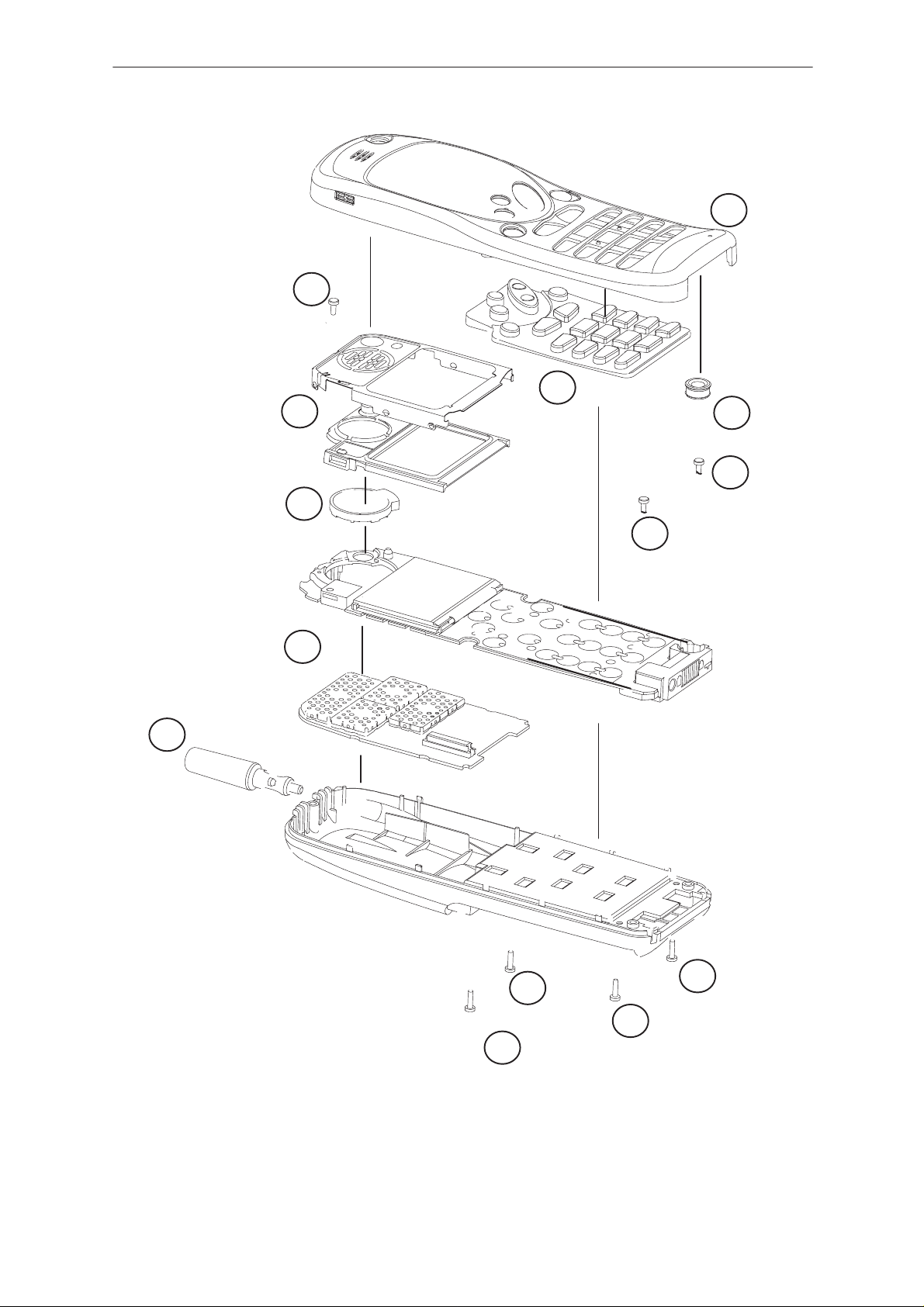
Disassembly Instructions
1. Antenna
Rotate anti–clockwise approximately 90 degrees and remove from top of
phone.
2. A Cover
A. Remove the battery pack (not shown).
B. Remove the four silver Torx screws. (2B)
C. Lift the A cover from the bottom end and it will come off.
D. The keymat is now loose.
3. Microphone
The microphone will now pull out of the system connector.
( Contact is made by two springs.)
4. PCB’s
Disassembly & Troubleshooting
A. Remove the three black Torx screws. (4A)
B. The UI and Engine PCB’s will lift out of the B cover. The PCB’s are held
together by a 44 way connector and can be pulled apart.
5. Engine PCB
The lids of the RF screens are removeable, however, once a lid has been
removed we recommended that you either solder it back to the frame of
the shield or replace it.
6. UI PCB
A. The metal speaker retainer is clipped to the PCB in six positions and
can be removed by easing it from the PCB.
B. The rubber gasket and the speaker are now free to be removed.
Issue 2 06/98
Page 3
Page 4
NHA–3
PAMS
Disassembly & Troubleshooting
4A
6A
6B
Technical Documentation
2C
2D
3
4A
4A
4B
1
2B
2B
Page 4
2B
2B
Issue 2 06/98
Page 5

PAMS
NHA–3
Technical Documentation
Troubleshooting Section
The purpose is to define fault block of the module and then find out the
broken component. The trouble shooting diagram has been planned so
that the fault, whatever it is, can be found by as simple measurements as
possible.
The flow diagrams give you the overview of the blocks. The purpose is
that you proceed through the flow diagram so that, if your answer is YES
for the asked question, go straight to the next level, but if your answer is
NO, you have to go the subbranch.
Required servicing equipment:
– NHA–3 Wintesla Service Software (product code: 8400597)
– Variable Power Supply Unit
– Digital multimeter
– Oscilloscope
Disassembly & Troubleshooting
– H700 Service Accessories
– MJS–2 Test Frame (NMP Part Number 0775095)
– RS232/MBUS adapter
– CMT/Marconi
– RF Spectrum Analyser
– Spectrum Analyser Probe HP85024A (300Khz to 3Ghz, attenuation
10:1)
Equipment Setup
In order for the faultfinding sections to be accurate, the servicing
equipment that is being used must be set to an identical state to when the
measurements were initially carried out. This section contains the settings
for the relevant faultfinding sections.
Issue 2 06/98
Page 5
Page 6

NHA–3
PAMS
Disassembly & Troubleshooting
Notes
Test Analyser Set Up
Generate – RF signal 881.400MHz, level –50dBm, 1KHz Tone – 8Khz deviation Connect
ADS–1 (Rx Audio) to AF Input and measure 1KHz tone (pk to pk)
Wintesla Set Up
Set phone to Local mode.
Set phone to Channel 380.
Audio set up as follows: Ex. Audio – ON
Tx. Audio – ON
Compressor – ON
Expander – ON
PA – ON
Level 2 – Volume Mid, X Mic
Notes T
Test Analyser Set Up
Set Tx Frequency to 836.400Mhz
Reciever Fault 1&2
ransmitter Fault 1&2
Technical Documentation
Wintesla Set Up
Set phone to Local mode.
Set phone to Channel 380.
Turn Tx On.
Page 6
Issue 2 06/98
Page 7

PAMS
NHA–3
Technical Documentation
General Chart
START
Will the phone turn into
Local Mode ?
Is phone Receiver OK?
Is phone transmitting OK?
Yes
Yes
No
No
No
Disassembly & Troubleshooting
Baseband Fault
Go to Receiver
Go to Transmitter Fault 1
Earphone level /
modulation
Is display / keypad
working ?
Call set–up ?
Yes
Yes
Yes
Yes
No
No
No
Earphone level or
modulation fault
Display or keypad fault
Call set–up fault
Issue 2 06/98
END
Page 7
Page 8

NHA–3
PAMS
Disassembly & Troubleshooting
Receiver Fault 1
soldering of
Check
V14
Yes
2.9Volts
Is N203 pin5
Is V14 pin3
Are VRXI
and RXBIAS
( V700/c ) 3.65 V
No
Yes
2.78Volts
Yes
( V700/b ) 2.6 V ?
Check : N203 pin1 =
– loading of Vrx
Vbatt, pin3 = logic1
– if OK, change N203
L8Check V14 pin3
Check :R47, R61,
N5 pin4
2.78Volts
Is ( VCC )
Yes
L5, C87, R51, R55, C93, C99
soldering of N5/pin9 and R63
Check IF demodulator circuit
Technical Documentation
–solderings of N5
– 2nd IF line N5/
Check :
Is there at
–the operation betwee
V11, C96 and C94
– d.c. voltages
– check solderings of Z18
Check :
3–5–10–11
–N5 at different pins
45 MHz ?
C705 – 60dBm
AF signal at
Noise or AF signal
No No No No No
Input to Receiver is –50dBm
*measured with 10:1 divider
Receiver fault
Simplex sens.
Yes
R63 RXAF line
D400/pin46 EarP
Yes
( TX off ) OK?
Earphone
level fault
Yes
No
No
Transmitter
fault
OK ?
TX spectrum
=2.78V
Test point
0.7 – 4.5Volts
RXVCO, middle channel
No
fault 2
Receiver
Yes
Replace duplex
filter Z10
Yes
Injection level
at C82 –20dBm
minimum
No
Check solderings of
G2,R42,C67
and C82
Yes
Is there at
44.55 MHz
N5/pin2 –34dBm
No
Check solderings
of R46,C79, C81, C84
and L6
Check also N5
?
pins 1 and 2.
V701,L3,C96 and C83
Check solderings of Z17
Yes
Is there level
No
Check the operation
No No
at Z17 –75dBm
between the aerial
and Z17
Yes
Yes Yes
C96 –88dBm
Check level at
45 MHz. OK ?
Page 8
Issue 2 06/98
Page 9

PAMS
NHA–3
Technical Documentation
Receiver Fault 2
Receiver fault 1
Check N3
Pin 18
5.2V?
Yes
Are N3
pins 4 and 14
2.7V?
Yes
Control signals
of N3/pins 8, 11, 12
13, 19 ( pin 8 –17dBm*/
14.85 MHz )
OK ?
Disassembly & Troubleshooting
*measured with 10:1 divider
No
No
No
Check NegVClk line
320kHz 3Vp–p
at C108
Check :
R37, R38 and Vrx
Check following lines for connectivity to
CTRLU D300
– N3/SYNDAT pin 12
– N3/SYNCLK pin 11
– N3/SYNDATENX pin 13
– N3/LOCKDET pin 19
Yes
Resistance
between N3/pin 3
and C32 5.6kOhms
Yes
Is RXVCO
oscillating at
C67?
Yes
Is level to
prescaler N3/
pin 6 – 30dBm* ?
Yes
Faulty Synthesiser N3
No
No
No
Fault in loop filter
Check:C30,
R35,C29,R16,C32
Check VCO supply voltage
at C61
Check C67 and C57
Issue 2 06/98
Page 9
Page 10

NHA–3
PAMS
Disassembly & Troubleshooting
Transmitter Fault 1
Baseband problem
No output on PWM
OK
Check soldering of R2/C7
NO
YES
V4 >1 Volt ?
Measure voltage at pin5
<1.5V
OK
Check PA soldering N1
C11/C6/C4 ?
Check soldering
on C20/C23/C5/C2
OK OK
soldering
Check Duplexer
Technical Documentation
NO
re–solder
NO
re–solder
NO
re–solder
Replace N1
if necessary
on N1 and reflow
Check connections
<3V ?
>1.5V
measure voltage at pin8
N1
Vary PAC 300 to 800
YES
>25dBm ?
at antenna clip
Measure O/P Power
YES
Tx Frequency OK
Low output power ?
NO
NO
>3V
NO
>–15dBm
Measure RF @ C14
NO
YES
>–20dBm ?
pin5 on N1 (PA)
Check RF level at
YES
NO
V3/R13/R11
at pin2 V4 >2V
Measure voltage
if not suspect V2
on R67/C14/R8
Check soldering
YES
across R14
1V to 0.6V ?
Measure volt drop
YES
YES
NO
>–20dBm
Measure RF at C18
YES
NO
at C16/C17
>–16dBm ?
Measure RF level
YES
NO
>2.5V <3V
at C9 (PAEN)
Measure voltage
YES
NO
around C9 and fix
Check for S/Circuits
NO
level<2dBm
and replace if output
connections Z7
Check SAW filter
C16/C17
Replace V5
Fault
AMSA/Baseband
mid – mid band
Transmitter Fault
Set Phone to PL2
*measured with 10:1 divider (20dB pad – No Offset in analyser)
Page 10
YES
>650mA ?
No Output power
High Current
YES
Check Frequencies /
levels at J4/J5
J5 = 90MHz >–35dBm ?
J4 = 914 to 939MHz
>–35dBm ?
NO
NO
90MHz OK ?
YES
YES
TX Fault 2
>–25dBm
and level at J3
Check frequency
824MHz to 849MHz
900MHz OK ?
NO
NO
RX Fault 2
Measure volt drop
Pin5 N2 >2.5Volt ?
across R10 >0.1Volt
NO
around mixer N2
replace if necessary
Check connections
Issue 2 06/98
Page 11

Issue 2 06/98
Transmitter fault 1
Transmitter Fault 2
Technical Documentation
PAMS
Resistance between
N3/pin 17 and V7
cathode is about 1.5kOhms
Check d.c.voltages
Yes Yes
VTX at J6 and 2.8V at V5 collector
OK ?
Check the critical
components of VCO :
R25,R34,R39,C21,C56,
C53 and check N3/pin 15. (85–95MHz@
~70mV
Disassembly & Troubleshooting
NoNo
Check VTX regulator V201 and that VTXEN
Fault in loop filter
Page 11
is low
NHA–3
Page 12

Page 12
Call set–up fault
Call Set–up Fault
NHA–3
Disassembly & Troubleshooting
Issue 2 06/98
Will the phone
assume SERV –mode ?
Check:
– the operation of ST signal
– the operation of SAT signal
– the operation of Transmitter
– the operation of TXI line
– the operation of Synthesizer
– the operation of VCO
– if OK, change N2
Yes
No
Subscriber
data OK ?
RSSI
operative ?
Data detection
of N2 operative ?
Yes
Yes
Yes
No
No
No
If the reprogramming
impossible, check D2
control lines and
solder joints.
Check N700/12/RSSI line
and the operation of
D1 A/D converters ( pins 78–85 ).
Inspect the signal path from
N700/pin 9 DAF to N2/ pin27.
Check also other lines
from N2.
Technical Documentation
Replace N2.
PAMS
Page 13

Issue 2 06/98
CONDTIONS ASSUMED:
VBATT = 3.6V
VCH = 6V
Logic fault
Power drops off or
does power up at all
OK with power key
but doesn’t wake up
with Charger?
Check clock
signal of D400 pin95
0.8 Vpp/14.85 MHz
When power key pressed
Check :
VCH at N200pin1 =6V?
R200,R201,R202
D400pin74 =1.2V?
D300pin65 = 1.2V?
C300
D301,R388,R389
VL (N201 pin 5)
Check:
– soldering of G1
NO
– C50. R418
– N3 pin 8 loading
– if OK, change G1
2.9V?
NO
Check :
–N201pin3 = 3.6V?
–N201 / N202 soldering
–C206 OK?
= VBATT OK?
VRX (N203 pin 5)
2.9V?
YES
VCTCXO (G1) VDD
2.9V +/–0.1?
Logic Fault
Check :
NOYES
– LowbattRSTX (D400pin2) = 2.9V
– Regen (N203pin3) = 2.9V
– OnRstX (D400pin3) = 2.9V
– PwrKeyX (D400pin73) = 0 when power key press
– VRX current loading
– If Ok change N203
NOYES
Check :
– R17/C24 components
Technical Documentation
PAMS
Page 13
YES
Is BBRstX = 0
at D300pin48
YES
Check AMSA PLL Functions:
– D400pin96 =2.9V (also R408/C409)
– R401, C402,C403.
– D400pins 92/93
– D400 supply VL/VA pins
NO
approx 8mA
How long is phone current
Drawn for after power key press?
approx 3–4mA for 16secs?
NO MCU control of AMSA: Check:
– D300 VL/GND pins
– D300 Mode pins 44,45,47,49 = 2.9V
– 4.8MHz clock at D300pin51
– MCU/AMSA communication: D7:0,A5:0,CS,RdX,Wr,X
.
for <500mS
MCU function OK. check:
– INTX signal OK? (D300pin70)
– Battmon AD. D300pin66 = 1.45V?
– Row lines OK? (D400pins 14;18)
– soldering of D301,R388,R389
Disassembly & Troubleshooting
NHA–3
Page 14

NHA–3
PAMS
Disassembly & Troubleshooting
Earphone Level/Modulation Level Fault
TEST CONDITIONS:
Using Wintesla audio testing window:–
– voice modulation 2.9 kHz
– XMIC line 31mVrms / 1kHz
– VDTRIM = 8
– VOLUME = 8
– Compressor and expander enabled
D400pin58
XMIC
D400pin71
TXO (TxMOD)
Technical Documentation
ST 678mVpp
88mVpp
(31mVrms) (87mVrms)
C400
RXAF
184mVpp
(65mVrms) (171mVrms)
246mVpp
843mVpp
D400pin77
RXgain
SAT 170mVpp
D400pin49
HEAR
117mVpp
(41mVrms)
Page 14
Issue 2 06/98
Page 15

PAMS
NHA–3
Technical Documentation
Display or Keypad Fault
UI PCB FAULT IDENTIFIED
Display or keypad fault
No
Display OK ?
Yes
Check display module
bonding
Display OK ?
Yes
Disassembly & Troubleshooting
Check:
– X500 pin 33 (VBB)
– LCDCLK 160kHz?
– LCDRstX = logic 1?
No
– LCD serial comunication signals:
LCDEnX, LCDDC, LDCSDCLK, LCDSDA
– Contrast setting resistors R612 / R613
– C600 to C607
Lights OK ?
Yes
Keypad
Problem
Pulses on
COL3:0
after key pressed
Yes
ROW 0–4 should be normally 2.9V
Pulsing to 0V with
corresponding key depressed.
Check those lines.
No No
No
X500 pins 40,41
light0/1
>2.7V with
lights on
Yes
Check the operation of
switches V601, V602, V603
Check COL 0–3 lines from D400.
R600, R601, R602, R603, R604
Check:
engine module D300pins 35,36
and X200 pins40/41
Issue 2 06/98
Page 15
Page 16

Page 16
Call set–up fault
Call Set–up Fault
NHA–3
Disassembly & Troubleshooting
Issue 2 06/98
Will the phone
assume SERV –mode ?
Yes
Check:
– the operation of ST signal
– the operation of SAT signal
– the operation of Transmitter
– the operation of Synthesizer
– the operation of UHF and 90MHz VCOs
– Check AFC function / Tx frequency error (no AFC)
No
Subscriber
data OK ?
Yes
RSSI
operative ?
Yes
RX data OK on D400pin77?
Yes
No
No
No
If the reprogramming
impossible, check EEPROM (D301)
control lines and
solder joints.
Check N5 pin12 RSSI line
and the operation of
D300 ADC (pin60)
Technical Documentation
Inspect the signal path from
N5 pin9 RXAF to D400pin77 (RXgain)
Replace D400
PAMS
 Loading...