

Page 1

Programmes After Market Services
NHA–3 Series Transceivers
Chapter 3
System Module
Issue 2 06/98
Page 2

NHA–3
System Module
Technical Documentation
CONTENTS
Introduction 3–5. . . . . . . . . . . . . . . . . . . . . . . . . . . . . . . . . . . . . . . . . . . . . . . . . . . . . .
Technical Specifications 3–5. . . . . . . . . . . . . . . . . . . . . . . . . . . . . . . . . . . . . . . . . . .
Modes of Operation 3–5. . . . . . . . . . . . . . . . . . . . . . . . . . . . . . . . . . . . . . . . . . .
External signals and connections. 3–5. . . . . . . . . . . . . . . . . . . . . . . . . . . . . . .
internal Signals 3–5. . . . . . . . . . . . . . . . . . . . . . . . . . . . . . . . . . . . . . . . . . . . . . .
Functional Description 3–6. . . . . . . . . . . . . . . . . . . . . . . . . . . . . . . . . . . . . . . . . . . .
Baseband Circuit Description 3–6. . . . . . . . . . . . . . . . . . . . . . . . . . . . . . . . . . .
General 3 6. . . . . . . . . . . . . . . . . . . . . . . . . . . . . . . . . . . . . . . . . . . . . . . . . . .
AMSA System Asic D400 3–8. . . . . . . . . . . . . . . . . . . . . . . . . . . . . . . . . .
AMSA D400 signals 3–8. . . . . . . . . . . . . . . . . . . . . . . . . . . . . . . . . . . . . . . .
PAMS
Page No
Microcontroller D300 3–9. . . . . . . . . . . . . . . . . . . . . . . . . . . . . . . . . . . . . . .
Microcontroller D300 signals 3–10. . . . . . . . . . . . . . . . . . . . . . . . . . . . . . . . .
EEPROM D301 3–11. . . . . . . . . . . . . . . . . . . . . . . . . . . . . . . . . . . . . . . . . . .
Regulation 3–1 1. . . . . . . . . . . . . . . . . . . . . . . . . . . . . . . . . . . . . . . . . . . . . . . .
CHAOS2 asic N200 and charging control 3–11. . . . . . . . . . . . . . . . . . . . . .
RF Circuit Description 3–12. . . . . . . . . . . . . . . . . . . . . . . . . . . . . . . . . . . . . . . . . .
Receiver 3–13. . . . . . . . . . . . . . . . . . . . . . . . . . . . . . . . . . . . . . . . . . . . . . . . . . . . .
Rx Synthesizer 3–14. . . . . . . . . . . . . . . . . . . . . . . . . . . . . . . . . . . . . . . . . . . . . . . .
Rx loop filter 3–14. . . . . . . . . . . . . . . . . . . . . . . . . . . . . . . . . . . . . . . . . . . . . . . . . .
Rx VCO 3–14. . . . . . . . . . . . . . . . . . . . . . . . . . . . . . . . . . . . . . . . . . . . . . . . . . . . . .
Tx synthesizer 3–15. . . . . . . . . . . . . . . . . . . . . . . . . . . . . . . . . . . . . . . . . . . . . . . .
TX VCO 3–15. . . . . . . . . . . . . . . . . . . . . . . . . . . . . . . . . . . . . . . . . . . . . . . . . . . . . .
Tx loop filter 3–15. . . . . . . . . . . . . . . . . . . . . . . . . . . . . . . . . . . . . . . . . . . . . . . . . .
Transmitter 3–15. . . . . . . . . . . . . . . . . . . . . . . . . . . . . . . . . . . . . . . . . . . . . . . . . . .
AFC function 3–16. . . . . . . . . . . . . . . . . . . . . . . . . . . . . . . . . . . . . . . . . . . . . . . . .
Parts List 3–17. . . . . . . . . . . . . . . . . . . . . . . . . . . . . . . . . . . . . . . . . . . . . . . . . . . . . . . .
Amps System Module Authenticated 3–17. . . . . . . . . . . . . . . . . . . . . . . . . . . . .
Namps System Module Authenticated 3–25. . . . . . . . . . . . . . . . . . . . . . . . . . . .
Page 3–2
Issue 2 06/98
Page 3

PAMS
NHA–3
Technical Documentation
System Module
List of Figures
PCB Version 10.1
Figure 1. Baseband Block Diagram 3–7. . . . . . . . . . . . . . . . . . . . . . . . . . . . . . . .
Figure 2. Rf Block Diagram 3–12. . . . . . . . . . . . . . . . . . . . . . . . . . . . . . . . . . . . . . .
Figure 3 System Block Diagram 3–A1. . . . . . . . . . . . . . . . . . . . . . . . . . . . . . . . . .
Figure 4 Baseband Block Diagram 3–A2. . . . . . . . . . . . . . . . . . . . . . . . . . . . . . . .
Figure 5 Asic Circuit Diagram 3–A3. . . . . . . . . . . . . . . . . . . . . . . . . . . . . . . . . . . .
Figure 6 CTRLU Circuit Diagram 3–A4. . . . . . . . . . . . . . . . . . . . . . . . . . . . . . . . .
Figure 7 PSU Circuit Diagram 3–A5. . . . . . . . . . . . . . . . . . . . . . . . . . . . . . . . . . .
Figure 8 RF Block Diagram 3–A6. . . . . . . . . . . . . . . . . . . . . . . . . . . . . . . . . . . . . .
Figure 9 RX Circuit Diagram 3–A7. . . . . . . . . . . . . . . . . . . . . . . . . . . . . . . . . . . . .
Figure 10 TX Circuit Diagram 3–A8. . . . . . . . . . . . . . . . . . . . . . . . . . . . . . . . . . . . . .
Page No
Figure 11 Component Layouts 3–A9. . . . . . . . . . . . . . . . . . . . . . . . . . . . . . . . . . . . .
Note: In printed manuals all A3 drawings are located at the back of the binder
Issue 2 06/98
Page 3–3
Page 4

NHA–3
System Module
PAMS
Technical Documentation
[This page intentionally left blank]
Page 3–4
Issue 2 06/98
Page 5

PAMS
NHA–3
Technical Documentation
Introduction
The H700 system module controls the operation of the transceiver.
These tasks include UI module control (keyboard, LCD, transducers,
accessory control), and all system signalling, audio processing , and RF
functions.
Technical Specifications
Modes of Operation
The module has 4 basic modes:
– Charging only: The phone is off, the only functions are battery charg-
ing
– Local mode: The phone is under external control via MBUS.
– Standby mode: the phone is ready to receive and make calls.
– Conversation mode: the phone is in a call, all RX and TX paths are ac-
tive.
System Module
External signals and connections.
The module has 2 connections:
– Board to board connector:
X200 44 way connector to the UI module.
– RF antenna connection:
X201 GND clip, X202 ANT clip.
The connectivity, functionality and performance of the board to board
connector is described in the UI module description. The pin numbering is
identical in the UI module and system module.
The performance of the antenna connection is described in the
Performance section
internal Signals
Table 3. Baseband / RF interface signals
Control signal Description
VBATT Battery supply voltage
GND Battery ground connection
PAC Filtered PWM power control signal for the transmitter
PAEN Power amplifier enable
VTX Regulated dc voltage for the low power transmitter stages
TXI Indicates when RF is present at the output of the transmitter
RXENX Enables the LNA, IF buffer ,FMIF and AFC buffer
VRX Regulated dc voltage for the receiver
Issue 2 06/98
Page 3–5
Page 6
NHA–3
System Module
Table 3. Baseband / RF interface signals (continued)
DescriptionControl signal
FSEL Selects AMPS/NAMPS 2nd IF filtering
RSSI Received signal strength indication
RXAF Received audio and data
IF2 2nd IF providing input to the AFC loop
LNABOOST Linearises the LNA in transmit mode
SYNDATENX Serial data enable for the synthesiser
SYNDAT Serial data bus for programming the synthesiser
SYNCLK Serial data clk input for the synthesiser
SYNTHENX Enables UHF VCO/buffer and controls synthesiser power down.
AFCDAC Voltage used to control TCXO output frequency
LOCKDET Indicates when synthesisers are in lock
TXMOD Modulation signal containing AMPS/NAMPS modulation
Technical Documentation
PAMS
REFFREQ VCTCXO output used to provide baseband clock
NEGVCLK Required for synthesiser voltage doubler
Functional Description
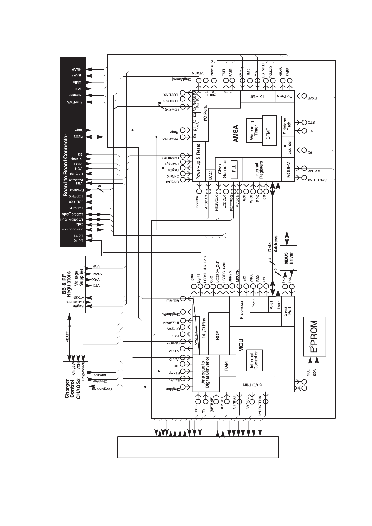
Baseband Circuit Description
General
The audio/logic unit consists of 4 ICs: AMSA system asic D400, MCU
D300, EEPROM D301, and CHAOS2 charger switch asic N200. These
ICs together with the supporting discrete circuitry make up the Baseband
block.
Page 3–6
Issue 2 06/98
Page 7
PAMS
NHA–3
Technical Documentation
System Module
Baseband Block Diagram
RF
Figure 1. Baseband Block Diagram
Issue 2 06/98
Page 3–7
Page 8
NHA–3
System Module
AMSA System Asic D400
AMSA is a 100pin TQFP mixed signal asic with the following functionality:
– Power–on / reset control, watchdog timer.
– Modem for AMPS/NAMPS
– Audio Processing for AMPS/NAMPS
– PLL and clock generation for BB system (using VTCXO as reference)
– I/O ports, allowing interrupt controlled MCU activity from keyboard and
accessories.
AMSA D400 signals
PAMS
Technical Documentation
pin
Power up / Reset /Clock generation signals
2 LowbattRstX Low battery reset input
3 OnRstX PLL–on reset delay input.
73 PwrKeyX Power key input for power on only
74 ChrgDet Charger detection input for power on only.
76 Regen VRX regulator and MCU enable.
20 MCUClk 4.8MHz MCU clock output
98 BBRstX MCU reset
4 NegVClk 320kHz clock for RF voltage doubler.
5 LCDClk 160kHz LCD clock output
92,93 PLLRC1,2 PLLRC filter connection for the 19.2Mhz AMSA PLL.
95 TCXO external 14.85MHz reference input for AMSA PLL
100 XIn Tied to GND, selects internal PLL.
AMSA / MCU interface
22 – 29 D7 – D0 Data bus
31 – 36 A0 – A5 AMSA Address bus
37 RdX AMSA read enable
38 WrX AMSA write enable
40 CS AMSA chip select
41 IntX MCU interrupt output
RF control signals
53 AFCDAC DAC output controlling VTCXO frequency
89 IF 450kHz 2nd IF counter input.
97 SYNTHENX Synth power enable (used for RX part in H700)
75 RXENX RX power enable (used for VCO supply enable in H700)
81 FMEN PLL PM modulation enable, for blocked channel elimination.
83 LNABOOST Open drain linearises the LNA in transmit mode
84 VTXEN VTX enable signal
85 FSEL AMPS/NAMPS filter selection
87 P AEN Transmit PA enable signal
label Function
Page 3–8
Issue 2 06/98
Page 9
PAMS
NHA–3
Technical Documentation
pin Functionlabel
UI / accessory control signals
7 (not used)
8 (not used)
9 ReqA Audio request accessory interrupt.
10 MBUS_AMSA MBUS detection produces an interupt
13 LCDRstX LCD reset signal
14 –18 Row (4:0) Keyboard Row0 to Row 4
Receive path signals
43 RxVMid DC bias for RX path. Decoupled to GND
77 RxGain Rx input amplifier feedback
78 RxIn Rx input amplifier input
49 HDSet Accessory external audio output (HEAR signal)
46 EARP Internal earpiece audio output
Transmit path signals
55 TxVMid DC bias for TX path. Decoupled to GND
58 XMic Accessory microphone audio input
59 BMic2 Internal microphone dc bias voltage.
60 BMic1 Headset dc bias / handsfree mute voltage.
61 CMic decoupling pin for BMiC
63 Mic2 Internal microphone audio input.
64 Mic1 Headset microphone audio input.
65, 68 MicGain 1 , 2 Mic amplifier gain feedback path
51, 69 STI,STO sidetone signal path
71 TxO Transmit modulation audio output to RF
82 BMicDis Discharge for BMic1 capacitor.
System Module
Microcontroller D300
This 80pin QFP MCU has the following features: internal ROM with code
protection, RAM, 8 channel 10bit A–D converter, Serial interface, and 6
configuarable I/0 ports.
Issue 2 06/98
Page 3–9
Page 10
NHA–3
System Module
Microcontroller D300 signals
PAMS
Technical Documentation
pin
1 PAC TX power control
3 BuzzPWM Buzzer signal to UI PCB
7 ChrgMonPull ChrgMon adjustment (high Z in reset, logic 0 when MCU
9 TxD MBUS transmit serial data
10 RxD MBUS receive serial data
13 – 20 D0 – D7 AMSA data bus
22 – 27 A0 – A5 AMSA address bus
31 Col0 Keypad–Matrix Column 0
32 Col1 Keypad–Matrix Column 1
33 Col2 Keypad–Matrix Column 2
34 Col3 Keypad–Matrix Column 3
35, 36 Light0, Light1 Backlighting control
37 IntEarEn Internal earpiece driver enable
39 RdX AMSA read control line
40 WrX AMSA write control line
41 CS AMSA chip select
59 RFTEMP RF temperature monitor
60 RSSI Signal strength indication
61 TXI Transmit Indicator
62 BTemp Battery temperature
63 BSI Battery size indication
64 AccID Accessory ID A–D input connected to ReqA
65 ChrgMon Charger voltage monitor
66 BattMon Battery voltage monitor
70 IntX AMSA interrupt
72 LOCKDET Synth lock detect
73 SYNCLK Synth Control, clock
74 SYNDAT Synth Control, data
75 ChrgCrtl ELVI fast charger control (32Hz)
76 SYNDATENX Synth Control, enable
77 VIBRA Vibration alert enable (10kHz), multiplexed onto BTEMP
78 SDA I2C Bus, data,
79 ChrgSW Charger switch control for Chaos2
80 SCL I2C Bus, clock
label Function
running.)
LCDDC Serial LCD driver data or command.
LCDSDA Serial LCD driver data
LCDSDCLK Serial LCD driver data clock
Page 3–10
Issue 2 06/98
Page 11

PAMS
NHA–3
Technical Documentation
EEPROM D301
This memory device contains non–volatile memory used to store user
defined memory locations, subscriber information, phone tuning data, and
production and service data. ESN is stored in protected one time
programmable section. Bi–directional communication is by serial I
to the MCU.
Regulation
There are 3 regulators producing the baseband and RF supplies. The
nominal voltage is 2.9V +/–0.1 for each regulator:
– Baseband regulator, N201, is the baseband supply from which VL, VA,
VPLL,and VBB is derived.
N201 is enabled by voltage detector N202, when VBATT is of a sufficient voltage to guarantee a valid baseband supply. If VBATT falls below the detector threshold, N200 will turn off the baseband supply and
put the phone into reset.
– VRX regulator, N203, is the supply for the RF receive section.
It is enabled by RegEn signal from AMSA’s power up block.
System Module
2
C bus
– VTX regulator , the supply for the low power RF TX section, is made
by discrete dual transistors V200, V201, and uses VRX as it’s reference.
It is enabled by software whenever the transmit path is required.
CHAOS2 asic N200 and charging control
CHAOS2 is basically an analog switch controlled by software, with some
additional integrated protection and start–up mechanisms.
When a charger is connected, CHAOS2 provides a start–up current of
60mA (nom) to VBATT, up to 4.0V(max). When SW recognises the
charger via ChrgMon A–D input on the MCU, it takes over control of the
charger current flow to the battery by controlling Chaos2 with the ChrgSW
signal.
ChrgMon has two ranges controlled by open drain ChrgMonAdj signal:
ChrgMonAdj=0 is the default. ChrgMonAdj = open is only used when
sensing current across CHAOS2 when using the 3 wire ELVI fast
chargers.
When phone is in reset, ChrgMonPull is high impedance to ensure there is
sufficient voltage on ChrgMon at AMSA pin74 to wake up the phone.
Issue 2 06/98
Page 3–11
Page 12

NHA–3
System Module
RF Circuit Description
PAMS
Technical Documentation
Power
Control
90MHz
VHF VCO
TXIF
Loop Filter
824 – 849 MHz
TXDUPI
Power
coupler
TXPAO
PA
TXPAI
Tx Filter
TXBO
824 – 849 MHz
TXMO
TXLO
Tx Mixer
Tx & Rx Synthesizer
VRXSYN
TXDUPO
4–pole
Duplexer
914 – 939MHz
UHF VCO
4–pole
4–pole
VRXVCO
PTXANT
869 – 894 MHz
PRXLO
LPF
LNA
Interstage
Filter
Rx Mixer
44.55MHz
X3
SAW
IF AMP
First IF Filter 45MHz
450KHz
FM IF Processor
AMPS NAMPS
GND
VBATT
PAEN
Page 3–12
VTX
VTCXO
14.85MHz
TXI
PAC
NEGVCLOCK
TXMOD
LOCKDET
SYNCLK
SYNDATENX
SYNDAT
REFFREQ
AFCDAC
SYNTHENX
RSSI
IF2
RXAF
RTEMP
FSEL
VRX
RXENX
LNABOOST
Figure 2. RF Block Diagram
Issue 2 06/98
Page 13

PAMS
NHA–3
Technical Documentation
Receiver
The receiver is a dual–conversion super–heterodyne using two
intermediate frequencies, 45 MHz and 450 kHz. The design implements
the necessary filtering and control required for NAMPS operation although
these components will not be fitted in AMPS only modules.
The RF signal from the duplexer RX port (via an additional low pass filter)
is applied to the RF amplifier. The amplifier is realized with transistor V10.
Amplifier stage input matching is accomplished with Z20 and Z23. R49,
R53, R47 and R52 are used for biasing. Output matching is carried out by
Z13 and Z14, R48 provides wideband stability. Components C86, and C85
are used for RF bypassing.
There is additional circuitry, R59 and C91, to boost the LNA current in Tx
mode.
Next the signal is filtered with Z17. The filter is followed by a single
balanced diode mixer, realized with a printed balun, C82, C83 and V9.
System Module
After the mixer the 45MHz IF signal is amplified with V11. The input
matching is realized with L7, C96, C102 and L9 which also forms a
22.5MHz notch. The purpose of this notch is to effectively improve the
IIP2 performance of the amplifier with respect to the half IF. The Output
matching is formed by L8, R44, C90 and C89.
After the IF amplifier the 45 MHz IF signal is filtered with crystal filter Z18.
Output matching is provided by R55 and dc blocked by C94.
The second mixer, the LO buffer transistor, IF amplifier and quadrature
detector are all integrated in the circuit N5. The second LO frequency,
44.55 MHz, is the third harmonic of the VCTXO frequency. The LO signal
is realized with tank circuit C81, C84 and L6. After the mixer the 450kHz
IF signal is filtered with ceramic filters Z22 (NAMPS) or Z11
(AMPS/NAMPS). Selection is made using an integrated switch N4. The IF
amplifier output signal is phase shifted by resonance circuit C99, C87,
R51 and L5. After this the signal is fed to a quadrature detector, this
multiplies the phase shifted signal with the original limited 450KHz IF.
The output of the limited 450KHz IF is buffered using V12 and associated
components. This is used for AFC.
Signal DAF is low pass filtered by R63 and C106. The DAF, RSSI and 2nd
IF signal (450 kHz) are fed to the AMSA ASIC.
Issue 2 06/98
Page 3–13
Page 14

NHA–3
System Module
Rx Synthesizer
The UHF LO signal is generated by a digital phase locked loop (PLL). The
output frequency of the loop is obtained from a voltage–controlled
oscillator (VCO). The loop gain, and hence the bandwidth, of the PLL
can be varied by data word programming. The VCO output signal is
sufficiently high enough to drive the receiver mixer. The injection level
required by the receiver mixer is about +2 dBm. In addition, the signal
from the VCO is fed to the synthesizer input and the transmit mixer LO
port.
The overall division ratio of the chain is selected within the synthesizer
according to the desired channel.
The internal dividers of the dual synthesizer are programmed serially on
the SDATA (synthesizer data) line from the processor into an internal shift
register also located in the synthesizer. Data transfer is timed with SCLK
clock pulses.
PAMS
Technical Documentation
The divided frequency is compared with a highly stable reference
frequency by a phase comparator in the PLL circuit. The phase
comparator controls the VCO frequency by means of a DC voltage
through the loop filter so as to keep the divided frequency applied to the
phase comparator equal to the fixed reference frequency.
The reference frequency is 10 kHz for both transmit and receive
synthesizers. This reference frequency is obtained from voltage controlled
crystal oscillator (VCXO). Oscillator frequency is 14.85 MHz. The VCXO
frequency is divided by 1485.
Rx Loop Filter
Phase comparator output is pin 3. If the VCO frequency is too high, the
output goes low and discharges the integrator capacitor C30. After this,
the DC control voltage and the VCO frequency will decrease.
If the VCO frequency is too low, the output goes high and charges the
integrator capacitor C30. Thereafter the DC control voltage and the VCO
frequency will go up.
Output pulses from the phase detector have to be supplied to the loop
filter. The function of the integrator is to convert positive and negative
pulses to a steady DC voltage. The remaining ripple and AC components
are filtered in the lowpass filter.
Rx VCO
Page 3–14
The VCO (circuit ref. G2) produces a level of +2 dBm level to the first Rx
mixer and delivers about –10dBm to both the synthesiser and the Tx
mixer.
Issue 2 06/98
Page 15

PAMS
NHA–3
Technical Documentation
Tx Synthesizer
The transmitter synthesizer generates a frequency modulated 90 MHz
fixed frequency signal for the transmitter section. The final output
frequency is generated by mixing the Rx LO with 90 MHz and extracting
the lower sideband.
The TX offset synthesizer consists of a 90 MHz PLL circuit, passive loop
filter and a 90 MHz VCO equipped with a chip coil resonator. The
bandwidth of the PLL can be varied by data word programming.
Modulation is brought to the VCO and applied to the opposite end of the
varactor.
See later for description of modulation filters.
TX VCO
The VCO is a Clapp type oscillator. The oscillator’s resonance frequency
is determined by a standard parallel LC tank circuit. The centre frequency
of the resonance circuit is adjustable only by use of the PLL and contains
no alignment. The VCO signal is fed directly to the prescaler and to the Tx
mixer.
System Module
Tx Loop Filter
Output current pulses from the phase detector are supplied to the loop
filter. These are then integrated, which converts positive and negative
current pulses to a DC voltage. The remaining ripple is filtered in the
low–pass filter accomplished with passive resistors and capacitors.
Transmitter
The modulated signal from the transmit mixer is applied to the input of
the transmit mixer buffer. This stage requires high gain and linearity, it’s
function is to amplify the transmit signal up to the required drive level for
the power amplifier.
The buffer must have good linearity to prevent the generation of
intermodulation products. The input of the amplifier is matched to the
mixer output impedance with the output of the amplifier directly matched
to 50 Ohms. The buffer is switched ON with the power amplifier enable
control signal.
The output of the transmit mixer buffer then passes through a SAW filter .
The filter is used to reduce the level of unwanted spurii and transmitter
noise due to the Tx mixer buffer, mixer and oscillator circuits. The output
of the filter drives directly into the PA MMIC.
Issue 2 06/98
Page 3–15
Page 16

NHA–3
System Module
The power amplifier is an integrated 2 stage RF gain block using GaAs
technology. The device is capable of +31.5dBm output power at 3.6V with
a minimum of 50% efficiency. Output power control is achieved by varying
the voltage on the VPC input. Internally VPC sets the bias to both stages
in the MMIC. There is no negative voltage required with this device.
ALC is used to maintain the power output over frequency, temperature
and battery voltage variation. The RF is detected via directional coupler
and Schottky diode. Rectified RF is compared with a filtered PWM
reference from baseband. This provides an error signal used to control a
series PNP transistor connected between VBATT and VPC.
The PWM signal must be filtered to prevent the generation of AM
sidebands. This filtering must be sufficient to reduce the sidebands and
also meet the power level switching time specification.
A TXI signal is used to prevent false transmissions. This signal is
monitored by the microprocessor and if the level is not appropriate for the
status of the transmitter, the PA is disabled.
PAMS
Technical Documentation
AFC Function
The transceiver unit is equipped with AFC function, i.e. it uses the
incoming receive signal from base station as a frequency reference. The
control loop consists of the receiver, the IF counter and an 8–bit D/A
converter in the AMSA ASIC and the VTCXO, which is used as a
reference oscillator of the synthesizer.
The 2nd IF signal (450 kHz) from the receiver is fed to AMSA. The IF
counter counts the received frequency. If the frequency differs from the
programmed value, the CPU adjusts the frequency of the VTCXO by
changing the output voltage of the D/A converter. This adjustment
continues until the desired receive frequency is achieved. AFC is not
active during a channel scan.
Page 3–16
Issue 2 06/98
Page 17

PAMS
NHA–3
Technical Documentation
Parts List
Amps System Module Authenticated
p.n 0200756 EDMS issue 11.11 PCB version 10.1
Item Code Description Value Type
R001 1430710 Chip resistor 22 5 % 0.063 W 0402
R002 1430778 Chip resistor 10 k 5 % 0.063 W 0402
R003 1430778 Chip resistor 10 k 5 % 0.063 W 0402
R004 1430758 Chip resistor 1.5 k 5 % 0.063 W 0402
R005 1430770 Chip resistor 4.7 k 5 % 0.063 W 0402
R006 1430762 Chip resistor 2.2 k 5 % 0.063 W 0402
R007 1430754 Chip resistor 1.0 k 5 % 0.063 W 0402
R008 1430718 Chip resistor 47 5 % 0.063 W 0402
R009 1430796 Chip resistor 47 k 5 % 0.063 W 0402
R010 1430796 Chip resistor 47 k 5 % 0.063 W 0402
R011 1430804 Chip resistor 100 k 5 % 0.063 W 0402
R012 1430772 Chip resistor 5.6 k 5 % 0.063 W 0402
R013 1430770 Chip resistor 4.7 k 5 % 0.063 W 0402
R014 1430718 Chip resistor 47 5 % 0.063 W 0402
R015 1430796 Chip resistor 47 k 5 % 0.063 W 0402
R016 1430772 Chip resistor 5.6 k 5 % 0.063 W 0402
R017 1430710 Chip resistor 22 5 % 0.063 W 0402
R018 1430784 Chip resistor 15 k 5 % 0.063 W 0402
R019 1430700 Chip resistor 10 5 % 0.063 W 0402
R020 1430744 Chip resistor 470 5 % 0.063 W 0402
R022 1430796 Chip resistor 47 k 5 % 0.063 W 0402
R023 1430778 Chip resistor 10 k 5 % 0.063 W 0402
R025 1430710 Chip resistor 22 5 % 0.063 W 0402
R026 1430762 Chip resistor 2.2 k 5 % 0.063 W 0402
R028 1430742 Chip resistor 390 5 % 0.063 W 0402
R029 1430690 Chip jumper 0402
R030 1430814 Chip resistor 270 k 5 % 0.063 W 0402
R032 1430758 Chip resistor 1.5 k 5 % 0.063 W 0402
R033 1430758 Chip resistor 1.5 k 5 % 0.063 W 0402
R034 1430754 Chip resistor 1.0 k 5 % 0.063 W 0402
R035 1430788 Chip resistor 22 k 5 % 0.063 W 0402
R037 1430714 Chip resistor 33 5 % 0.063 W 0402
R038 1430714 Chip resistor 33 5 % 0.063 W 0402
R039 1430760 Chip resistor 1.8 k 5 % 0.063 W 0402
R040 1430754 Chip resistor 1.0 k 5 % 0.063 W 0402
R042 1430710 Chip resistor 22 5 % 0.063 W 0402
R044 1430742 Chip resistor 390 5 % 0.063 W 0402
System Module
Issue 2 06/98
Page 3–17
Page 18

NHA–3
System Module
R046 1430778 Chip resistor 10 k 5 % 0.063 W 0402
R047 1430732 Chip resistor 180 5 % 0.063 W 0402
R048 1430734 Chip resistor 220 5 % 0.063 W 0402
R049 1430772 Chip resistor 5.6 k 5 % 0.063 W 0402
R050 1430720 Chip resistor 56 5 % 0.063 W 0402
R051 1430772 Chip resistor 5.6 k 5 % 0.063 W 0402
R052 1430762 Chip resistor 2.2 k 5 % 0.063 W 0402
R053 1430776 Chip resistor 8.2 k 5 % 0.063 W 0402
R054 1430700 Chip resistor 10 5 % 0.063 W 0402
R055 1430760 Chip resistor 1.8 k 5 % 0.063 W 0402
R056 1430758 Chip resistor 1.5 k 5 % 0.063 W 0402
R057 1430784 Chip resistor 15 k 5 % 0.063 W 0402
R058 1430758 Chip resistor 1.5 k 5 % 0.063 W 0402
R059 1430770 Chip resistor 4.7 k 5 % 0.063 W 0402
R061 1430726 Chip resistor 100 5 % 0.063 W 0402
R062 1430832 Chip resistor 2.7 k 5 % 0.063 W 0402
R063 1430770 Chip resistor 4.7 k 5 % 0.063 W 0402
R064 1430778 Chip resistor 10 k 5 % 0.063 W 0402
R067 1430718 Chip resistor 47 5 % 0.063 W 0402
R068 1430700 Chip resistor 10 5 % 0.063 W 0402
R069 1430151 Chip resistor 10 5 % 0.063 W 0603
R070 1430730 Chip resistor 150 5 % 0.063 W 0402
R073 1430738 Chip resistor 270 5 % 0.063 W 0402
R074 1430754 Chip resistor 1.0 k 5 % 0.063 W 0402
R075 1430690 Chip jumper 0402
R200 1430800 Chip resistor 68 k 5 % 0.063 W 0402
R201 1430814 Chip resistor 270 k 5 % 0.063 W 0402
R202 1430810 Chip resistor 180 k 5 % 0.063 W 0402
R203 1430814 Chip resistor 270 k 5 % 0.063 W 0402
R204 1430810 Chip resistor 180 k 5 % 0.063 W 0402
R206 1430804 Chip resistor 100 k 5 % 0.063 W 0402
R207 1430788 Chip resistor 22 k 5 % 0.063 W 0402
R210 1430762 Chip resistor 2.2 k 5 % 0.063 W 0402
R301 1430778 Chip resistor 10 k 5 % 0.063 W 0402
R302 1430796 Chip resistor 47 k 5 % 0.063 W 0402
R303 1430796 Chip resistor 47 k 5 % 0.063 W 0402
R304 1430754 Chip resistor 1.0 k 5 % 0.063 W 0402
R305 1430778 Chip resistor 10 k 5 % 0.063 W 0402
R306 1430778 Chip resistor 10 k 5 % 0.063 W 0402
R307 1430796 Chip resistor 47 k 5 % 0.063 W 0402
R308 1430796 Chip resistor 47 k 5 % 0.063 W 0402
R309 1430796 Chip resistor 47 k 5 % 0.063 W 0402
R310 1430796 Chip resistor 47 k 5 % 0.063 W 0402
Technical Documentation
PAMS
Page 3–18
Issue 2 06/98
Page 19

PAMS
NHA–3
Technical Documentation
R311 1430788 Chip resistor 22 k 5 % 0.063 W 0402
R313 1430778 Chip resistor 10 k 5 % 0.063 W 0402
R400 1430778 Chip resistor 10 k 5 % 0.063 W 0402
R401 1430776 Chip resistor 8.2 k 5 % 0.063 W 0402
R403 1430788 Chip resistor 22 k 5 % 0.063 W 0402
R405 1430804 Chip resistor 100 k 5 % 0.063 W 0402
R406 1430786 Chip resistor 18 k 5 % 0.063 W 0402
R407 1430810 Chip resistor 180 k 5 % 0.063 W 0402
R408 1430726 Chip resistor 100 5 % 0.063 W 0402
R409 1430814 Chip resistor 270 k 5 % 0.063 W 0402
R410 1430762 Chip resistor 2.2 k 5 % 0.063 W 0402
R411 1430762 Chip resistor 2.2 k 5 % 0.063 W 0402
R412 1430814 Chip resistor 270 k 5 % 0.063 W 0402
R413 1430796 Chip resistor 47 k 5 % 0.063 W 0402
R416 1430804 Chip resistor 100 k 5 % 0.063 W 0402
R417 1430796 Chip resistor 47 k 5 % 0.063 W 0402
R418 1430762 Chip resistor 2.2 k 5 % 0.063 W 0402
C001 2320552 Ceramic cap. 47 p 5 % 50 V 0402
C002 2312410 Ceramic cap. 1.0 u 10 % 16 V 1206
C003 2320620 Ceramic cap. 10 n 5 % 16 V 0402
C004 2320552 Ceramic cap. 47 p 5 % 50 V 0402
C005 2320620 Ceramic cap. 10 n 5 % 16 V 0402
C006 2320552 Ceramic cap. 47 p 5 % 50 V 0402
C007 2320620 Ceramic cap. 10 n 5 % 16 V 0402
C009 2320620 Ceramic cap. 10 n 5 % 16 V 0402
C010 2320620 Ceramic cap. 10 n 5 % 16 V 0402
C011 2320534 Ceramic cap. 8.2 p 0.25 % 50 V 0402
C012 2312410 Ceramic cap. 1.0 u 10 % 16 V 1206
C013 2320552 Ceramic cap. 47 p 5 % 50 V 0402
C014 2320552 Ceramic cap. 47 p 5 % 50 V 0402
C015 2320781 Ceramic cap. 47 n 20 % 16 V 0603
C016 2320602 Ceramic cap. 4.7 p 0.25 % 50 V 0402
C017 2320530 Ceramic cap. 5.6 p 0.25 % 50 V 0402
C018 2320552 Ceramic cap. 47 p 5 % 50 V 0402
C019 2320552 Ceramic cap. 47 p 5 % 50 V 0402
C020 2320534 Ceramic cap. 8.2 p 0.25 % 50 V 0402
C021 2611668 Tantalum cap. 4.7 u 20 % 10 V 3.2x1.6x1.6
C022 2320552 Ceramic cap. 47 p 5 % 50 V 0402
C023 2320602 Ceramic cap. 4.7 p 0.25 % 50 V 0402
C024 2320781 Ceramic cap. 47 n 20 % 16 V 0603
C025 2320546 Ceramic cap. 27 p 5 % 50 V 0402
C026 2320552 Ceramic cap. 47 p 5 % 50 V 0402
C029 2310011 Ceramic cap. 150 n 10 % 16 V 0805
System Module
Issue 2 06/98
Page 3–19
Page 20

NHA–3
System Module
C030 2320109 Ceramic cap. 15 n 5 % 25 V 0603
C032 2320109 Ceramic cap. 15 n 5 % 25 V 0603
C033 2320520 Ceramic cap. 2.2 p 0.25 % 50 V 0402
C035 2611668 Tantalum cap. 4.7 u 20 % 10 V 3.2x1.6x1.6
C038 2320618 Ceramic cap. 4.7 n 5 % 25 V 0402
C039 2320552 Ceramic cap. 47 p 5 % 50 V 0402
C042 2320779 Ceramic cap. 100 n 10 % 16 V 0603
C043 2320538 Ceramic cap. 12 p 5 % 50 V 0402
C045 2320546 Ceramic cap. 27 p 5 % 50 V 0402
C046 2320779 Ceramic cap. 100 n 10 % 16 V 0603
C047 2610017 Tantalum cap. 33 u 20 % 10 V 6.0x3.2x2.5
C048 2320544 Ceramic cap. 22 p 5 % 50 V 0402
C050 2320620 Ceramic cap. 10 n 5 % 16 V 0402
C052 2320552 Ceramic cap. 47 p 5 % 50 V 0402
C053 2320544 Ceramic cap. 22 p 5 % 50 V 0402
C054 2320560 Ceramic cap. 100 p 5 % 50 V 0402
C055 2320620 Ceramic cap. 10 n 5 % 16 V 0402
C056 2320544 Ceramic cap. 22 p 5 % 50 V 0402
C057 2320602 Ceramic cap. 4.7 p 0.25 % 50 V 0402
C058 2320744 Ceramic cap. 1.0 n 10 % 50 V 0402
C060 2320618 Ceramic cap. 4.7 n 5 % 25 V 0402
C061 2610003 Tantalum cap. 10 u 20 % 10 V 3.2x1.6x1.6
C062 2611668 Tantalum cap. 4.7 u 20 % 10 V 3.2x1.6x1.6
C063 2320544 Ceramic cap. 22 p 5 % 50 V 0402
C064 2320620 Ceramic cap. 10 n 5 % 16 V 0402
C065 2320550 Ceramic cap. 39 p 5 % 50 V 0402
C067 2320540 Ceramic cap. 15 p 5 % 50 V 0402
C070 2320781 Ceramic cap. 47 n 20 % 16 V 0603
C072 2320546 Ceramic cap. 27 p 5 % 50 V 0402
C074 2320781 Ceramic cap. 47 n 20 % 16 V 0603
C075 2320620 Ceramic cap. 10 n 5 % 16 V 0402
C076 2320620 Ceramic cap. 10 n 5 % 16 V 0402
C079 2320620 Ceramic cap. 10 n 5 % 16 V 0402
C080 2320540 Ceramic cap. 15 p 5 % 50 V 0402
C081 2320570 Ceramic cap. 270 p 5 % 50 V 0402
C082 2320526 Ceramic cap. 3.9 p 0.25 % 50 V 0402
C083 2320151 Ceramic cap. 50 V 0402
C084 2320546 Ceramic cap. 27 p 5 % 50 V 0402
C085 2320556 Ceramic cap. 68 p 5 % 50 V 0402
C086 2320744 Ceramic cap. 1.0 n 10 % 50 V 0402
C087 2310490 Ceramic cap. 360 p 2 % 50 V 0805
C088 2320534 Ceramic cap. 8.2 p 0.25 % 50 V 0402
C089 2320534 Ceramic cap. 8.2 p 0.25 % 50 V 0402
Technical Documentation
PAMS
Page 3–20
Issue 2 06/98
Page 21

PAMS
NHA–3
Technical Documentation
C090 2320548 Ceramic cap. 33 p 5 % 50 V 0402
C091 2320546 Ceramic cap. 27 p 5 % 50 V 0402
C092 2320514 Ceramic cap. 1.2 p 0.25 % 50 V 0402
C093 2320781 Ceramic cap. 47 n 20 % 16 V 0603
C094 2320620 Ceramic cap. 10 n 5 % 16 V 0402
C095 2320620 Ceramic cap. 10 n 5 % 16 V 0402
C096 2320584 Ceramic cap. 1.0 n 5 % 50 V 0402
C097 2320522 Ceramic cap. 2.7 p 0.25 % 50 V 0402
C099 2320548 Ceramic cap. 33 p 5 % 50 V 0402
C100 2320618 Ceramic cap. 4.7 n 5 % 25 V 0402
C101 2320546 Ceramic cap. 27 p 5 % 50 V 0402
C102 2320564 Ceramic cap. 150 p 5 % 50 V 0402
C103 2320522 Ceramic cap. 2.7 p 0.25 % 50 V 0402
C104 2312410 Ceramic cap. 1.0 u 10 % 16 V 1206
C105 2320546 Ceramic cap. 27 p 5 % 50 V 0402
C106 2320584 Ceramic cap. 1.0 n 5 % 50 V 0402
C107 2312293 Ceramic cap. Y5 V 1206
C108 2611668 Tantalum cap. 4.7 u 20 % 10 V 3.2x1.6x1.6
C115 2320620 Ceramic cap. 10 n 5 % 16 V 0402
C116 2320546 Ceramic cap. 27 p 5 % 50 V 0402
C117 2320546 Ceramic cap. 27 p 5 % 50 V 0402
C118 2320546 Ceramic cap. 27 p 5 % 50 V 0402
C200 2312296 Ceramic cap. Y5 V 1210
C201 2611668 Tantalum cap. 4.7 u 20 % 10 V 3.2x1.6x1.6
C203 2320620 Ceramic cap. 10 n 5 % 16 V 0402
C205 2611668 Tantalum cap. 4.7 u 20 % 10 V 3.2x1.6x1.6
C206 2320620 Ceramic cap. 10 n 5 % 16 V 0402
C207 2611668 Tantalum cap. 4.7 u 20 % 10 V 3.2x1.6x1.6
C208 2312292 Ceramic cap. 470 n 20 % Y5 V 1210
C209 2320546 Ceramic cap. 27 p 5 % 50 V 0402
C300 2320620 Ceramic cap. 10 n 5 % 16 V 0402
C301 2320620 Ceramic cap. 10 n 5 % 16 V 0402
C302 2320781 Ceramic cap. 47 n 20 % 16 V 0603
C304 2320620 Ceramic cap. 10 n 5 % 16 V 0402
C305 2320620 Ceramic cap. 10 n 5 % 16 V 0402
C306 2320620 Ceramic cap. 10 n 5 % 16 V 0402
C401 2320779 Ceramic cap. 100 n 10 % 16 V 0603
C402 2320781 Ceramic cap. 47 n 20 % 16 V 0603
C403 2320620 Ceramic cap. 10 n 5 % 16 V 0402
C404 2320781 Ceramic cap. 47 n 20 % 16 V 0603
C405 2320781 Ceramic cap. 47 n 20 % 16 V 0603
C406 2320781 Ceramic cap. 47 n 20 % 16 V 0603
C407 2320781 Ceramic cap. 47 n 20 % 16 V 0603
System Module
Issue 2 06/98
Page 3–21
Page 22

NHA–3
System Module
C408 2320781 Ceramic cap. 47 n 20 % 16 V 0603
C409 2611668 Tantalum cap. 4.7 u 20 % 10 V 3.2x1.6x1.6
C410 2320781 Ceramic cap. 47 n 20 % 16 V 0603
C411 2320781 Ceramic cap. 47 n 20 % 16 V 0603
C412 2320620 Ceramic cap. 10 n 5 % 16 V 0402
C413 2320620 Ceramic cap. 10 n 5 % 16 V 0402
C416 2312410 Ceramic cap. 1.0 u 10 % 16 V 1206
C417 2320546 Ceramic cap. 27 p 5 % 50 V 0402
L002 3641574 Chip coil 68 n 5 % Q=40/200 MHz 0805
L004 3643033 Chip coil 120 n 5 % Q=40/150 MHz 0805
L005 3640103 Chip coil 320 u 2 % Q=40/796 kHz 1812
L006 3608407 Chip coil 470 n 5 % 1206
L007 3641574 Chip coil 68 n 5 % Q=40/200 MHz 0805
L008 3608519 Chip coil 5 % Q=28/35 MHz 1206
L009 3645031 Chip coil 330 n 10 % Q=20/25 MHz 0805
L010 3641522 Chip coil 6 n 20 % Q=50/250 MHz 0805
G001 4510111 VCTCXO 14.85 M +–2PPM 3.0V
G002 4350079 Vco 914–939mhz 2.55v 12ma
Z007 4510091 Saw filter 836.5+–12.5M
Z010 4510093 Dupl 824–849/869–894mhz
Z011 4550019 Cer.filt 450+–14khz
Z017 4510089 Saw filter 881.5+–12.5M
Z018 4510087 XTAL filter 45M +–14KHZ AMPS
V001 4219922 Transistor x 2 UM6
V002 4100567 Sch. diode x 2 BAS70–04 70V15 mA SERSOT23
V003 4210102 Transistor BC858W pnp 30V 100mA 200MWSOT323
V004 4219904 Transistor x 2 UMX1 npn 40V SOT363
V005 4210010 Transistor BFP183 npn 12V 65mA SOT143
V006 4210079 Transistor BFS17 npn 15V 50mA SOT23
V007 4104951 Cap. diode x 2 BBY39 SOT23
V009 4115802 Sch. diode x 2 4V 30mA SOT23
V010 4210074 Transistor BFP420 npn 4V SOT343
V011 4210066 Transistor BFR93AW npn 12V 35mA SOT323
V012 4210100 Transistor BC848W npn 30V SOT323
V013 4100567 Sch. diode x 2 BAS70–04 70V 15mA SERSOT23
V014 4219927 Transistor x 2 RX2 UMB4 pnp 50V 0. A UM6
V200 4219922 Transistor x 2 UM6
V201 4219904 Transistor x 2 UMX1 npn 40V SOT363
V202 4110072 Diode x 2 BAV99W 70V 0.2A SOT323
V301 4210100 Transistor BC848W npn 30V SOT323
D300 0240235 Spb4 programmed prom h700
D301 4340251 IC, EEPROM NMP40251 SO8S
D400 4370033 Amsa tcm9106 asic mix/sig PQFP100
Technical Documentation
PAMS
Page 3–22
Issue 2 06/98
Page 23

PAMS
NHA–3
Technical Documentation
N001 4370099 Rf9102 pw amp 824–849mhz SO16SQB
N002 4340171 IC, upconv 1.9ghz 3v SO6S
N003 4340197 IC, PLL MB15U10 SSO20
N005 4349694 IC, if amp+fm detector TA31136 SSO16
N200 4370237 Chaos2.charger on/off switch ASIC
N201 4340225 IC, regulator LP2980I–2.9 SSO5
N202 4340259 S80728sl–at–t1 v–detector SOT23–5
N203 4340225 IC, regulator LP2980I–2.9 SSO5
X200 5469051 PCB connector 44way p0.65 recept.
X201 9510346 Feed contact dmd01170 nha–3na
X202 9510347 Earth contact dmd02110 nha–3na
A001 9517008 Shield assembly–1 dmc00505
A002 9517009 Shield assembly–2 dmc00506
A003 9517010 Shield assembly–3 dmc00507
A004 9517011 Shield assembly–4 dmc00508
A005 9517010 Shield assembly–3 dmc00507
P001 9850024 PC board PC4
System Module
Issue 2 06/98
Page 3–23
Page 24

NHA–3
System Module
PAMS
Technical Documentation
[This page intentionally left blank]
Page 3–24
Issue 2 06/98
Page 25

PAMS
NHA–3
Technical Documentation
Namps System Module Authenticated
p.n 0201066 EDMS issue 1.8
Item Code Description Value Type
R001 1430710 Chip resistor 22 5 % 0.063 W 0402
R002 1430778 Chip resistor 10 k 5 % 0.063 W 0402
R003 1430778 Chip resistor 10 k 5 % 0.063 W 0402
R004 1430758 Chip resistor 1.5 k 5 % 0.063 W 0402
R005 1430770 Chip resistor 4.7 k 5 % 0.063 W 0402
R006 1430762 Chip resistor 2.2 k 5 % 0.063 W 0402
R007 1430754 Chip resistor 1.0 k 5 % 0.063 W 0402
R008 1430718 Chip resistor 47 5 % 0.063 W 0402
R009 1430796 Chip resistor 47 k 5 % 0.063 W 0402
R010 1430796 Chip resistor 47 k 5 % 0.063 W 0402
R011 1430804 Chip resistor 100 k 5 % 0.063 W 0402
R012 1430772 Chip resistor 5.6 k 5 % 0.063 W 0402
R013 1430770 Chip resistor 4.7 k 5 % 0.063 W 0402
R014 1430718 Chip resistor 47 5 % 0.063 W 0402
R015 1430796 Chip resistor 47 k 5 % 0.063 W 0402
R016 1430772 Chip resistor 5.6 k 5 % 0.063 W 0402
R017 1430710 Chip resistor 22 5 % 0.063 W 0402
R018 1430784 Chip resistor 15 k 5 % 0.063 W 0402
R020 1430744 Chip resistor 470 5 % 0.063 W 0402
R022 1430796 Chip resistor 47 k 5 % 0.063 W 0402
R023 1430778 Chip resistor 10 k 5 % 0.063 W 0402
R025 1430710 Chip resistor 22 5 % 0.063 W 0402
R028 1430742 Chip resistor 390 5 % 0.063 W 0402
R031 1430760 Chip resistor 1.8 k 5 % 0.063 W 0402
R032 1430758 Chip resistor 1.5 k 5 % 0.063 W 0402
R033 1430758 Chip resistor 1.5 k 5 % 0.063 W 0402
R034 1430758 Chip resistor 1.5 k 5 % 0.063 W 0402
R035 1430788 Chip resistor 22 k 5 % 0.063 W 0402
R037 1430714 Chip resistor 33 5 % 0.063 W 0402
R038 1430714 Chip resistor 33 5 % 0.063 W 0402
R039 1430832 Chip resistor 2.7 k 5 % 0.063 W 0402
R040 1430762 Chip resistor 2.2 k 5 % 0.063 W 0402
R042 1430710 Chip resistor 22 5 % 0.063 W 0402
R044 1430742 Chip resistor 390 5 % 0.063 W 0402
R046 1430778 Chip resistor 10 k 5 % 0.063 W 0402
R047 1430732 Chip resistor 180 5 % 0.063 W 0402
R048 1430734 Chip resistor 220 5 % 0.063 W 0402
R049 1430772 Chip resistor 5.6 k 5 % 0.063 W 0402
R050 1430720 Chip resistor 56 5 % 0.063 W 0402
System Module
Issue 2 06/98
Page 3–25
Page 26

NHA–3
System Module
R051 1430772 Chip resistor 5.6 k 5 % 0.063 W 0402
R052 1430762 Chip resistor 2.2 k 5 % 0.063 W 0402
R053 1430776 Chip resistor 8.2 k 5 % 0.063 W 0402
R055 1430760 Chip resistor 1.8 k 5 % 0.063 W 0402
R056 1430758 Chip resistor 1.5 k 5 % 0.063 W 0402
R057 1430784 Chip resistor 15 k 5 % 0.063 W 0402
R058 1430758 Chip resistor 1.5 k 5 % 0.063 W 0402
R059 1430770 Chip resistor 4.7 k 5 % 0.063 W 0402
R060 1430720 Chip resistor 56 5 % 0.063 W 0402
R061 1430726 Chip resistor 100 5 % 0.063 W 0402
R062 1430832 Chip resistor 2.7 k 5 % 0.063 W 0402
R063 1430770 Chip resistor 4.7 k 5 % 0.063 W 0402
R064 1430778 Chip resistor 10 k 5 % 0.063 W 0402
R067 1430718 Chip resistor 47 5 % 0.063 W 0402
R070 1430738 Chip resistor 270 5 % 0.063 W 0402
R073 1430738 Chip resistor 270 5 % 0.063 W 0402
R074 1430754 Chip resistor 1.0 k 5 % 0.063 W 0402
R075 1430700 Chip resistor 10 5 % 0.063 W 0402
R076 1430780 Chip resistor 12 k 5 % 0.063 W 0402
R077 1430786 Chip resistor 18 k 5 % 0.063 W 0402
R078 1430800 Chip resistor 68 k 5 % 0.063 W 0402
R200 1430800 Chip resistor 68 k 5 % 0.063 W 0402
R201 1430814 Chip resistor 270 k 5 % 0.063 W 0402
R202 1430810 Chip resistor 180 k 5 % 0.063 W 0402
R203 1430814 Chip resistor 270 k 5 % 0.063 W 0402
R204 1430810 Chip resistor 180 k 5 % 0.063 W 0402
R206 1430804 Chip resistor 100 k 5 % 0.063 W 0402
R207 1430788 Chip resistor 22 k 5 % 0.063 W 0402
R210 1430762 Chip resistor 2.2 k 5 % 0.063 W 0402
R301 1430778 Chip resistor 10 k 5 % 0.063 W 0402
R302 1430796 Chip resistor 47 k 5 % 0.063 W 0402
R303 1430796 Chip resistor 47 k 5 % 0.063 W 0402
R304 1430754 Chip resistor 1.0 k 5 % 0.063 W 0402
R305 1430778 Chip resistor 10 k 5 % 0.063 W 0402
R306 1430778 Chip resistor 10 k 5 % 0.063 W 0402
R307 1430796 Chip resistor 47 k 5 % 0.063 W 0402
R308 1430796 Chip resistor 47 k 5 % 0.063 W 0402
R309 1430796 Chip resistor 47 k 5 % 0.063 W 0402
R310 1430796 Chip resistor 47 k 5 % 0.063 W 0402
R311 1430788 Chip resistor 22 k 5 % 0.063 W 0402
R312 1430754 Chip resistor 1.0 k 5 % 0.063 W 0402
R313 1430778 Chip resistor 10 k 5 % 0.063 W 0402
R400 1430778 Chip resistor 10 k 5 % 0.063 W 0402
Technical Documentation
PAMS
Page 3–26
Issue 2 06/98
Page 27

PAMS
NHA–3
Technical Documentation
R401 1430776 Chip resistor 8.2 k 5 % 0.063 W 0402
R403 1430788 Chip resistor 22 k 5 % 0.063 W 0402
R405 1430804 Chip resistor 100 k 5 % 0.063 W 0402
R406 1430786 Chip resistor 18 k 5 % 0.063 W 0402
R407 1430810 Chip resistor 180 k 5 % 0.063 W 0402
R408 1430726 Chip resistor 100 5 % 0.063 W 0402
R409 1430814 Chip resistor 270 k 5 % 0.063 W 0402
R410 1430762 Chip resistor 2.2 k 5 % 0.063 W 0402
R411 1430762 Chip resistor 2.2 k 5 % 0.063 W 0402
R412 1430814 Chip resistor 270 k 5 % 0.063 W 0402
R413 1430796 Chip resistor 47 k 5 % 0.063 W 0402
R416 1430804 Chip resistor 100 k 5 % 0.063 W 0402
R417 1430796 Chip resistor 47 k 5 % 0.063 W 0402
R418 1430762 Chip resistor 2.2 k 5 % 0.063 W 0402
C001 2320552 Ceramic cap. 47 p 5 % 50 V 0402
C002 2312410 Ceramic cap. 1.0 u 10 % 16 V 1206
C003 2320620 Ceramic cap. 10 n 5 % 16 V 0402
C004 2320552 Ceramic cap. 47 p 5 % 50 V 0402
C005 2320620 Ceramic cap. 10 n 5 % 16 V 0402
C006 2320552 Ceramic cap. 47 p 5 % 50 V 0402
C007 2320620 Ceramic cap. 10 n 5 % 16 V 0402
C009 2320620 Ceramic cap. 10 n 5 % 16 V 0402
C010 2320620 Ceramic cap. 10 n 5 % 16 V 0402
C011 2320534 Ceramic cap. 8.2 p 0.25 % 50 V 0402
C012 2312410 Ceramic cap. 1.0 u 10 % 16 V 1206
C013 2320552 Ceramic cap. 47 p 5 % 50 V 0402
C014 2320552 Ceramic cap. 47 p 5 % 50 V 0402
C015 2320781 Ceramic cap. 47 n 20 % 16 V 0603
C016 2320602 Ceramic cap. 4.7 p 0.25 % 50 V 0402
C017 2320530 Ceramic cap. 5.6 p 0.25 % 50 V 0402
C018 2320552 Ceramic cap. 47 p 5 % 50 V 0402
C019 2320552 Ceramic cap. 47 p 5 % 50 V 0402
C020 2320534 Ceramic cap. 8.2 p 0.25 % 50 V 0402
C021 2611668 Tantalum cap. 4.7 u 20 % 10 V 3.2x1.6x1.6
C022 2320552 Ceramic cap. 47 p 5 % 50 V 0402
C023 2320602 Ceramic cap. 4.7 p 0.25 % 50 V 0402
C024 2320781 Ceramic cap. 47 n 20 % 16 V 0603
C025 2320546 Ceramic cap. 27 p 5 % 50 V 0402
C026 2320552 Ceramic cap. 47 p 5 % 50 V 0402
C028 2611668 Tantalum cap. 4.7 u 20 % 10 V 3.2x1.6x1.6
C029 2310011 Ceramic cap. 150 n 10 % 16 V 0805
C030 2320120 Ceramic cap. 22 n 10 % 25 V 0603
C032 2320120 Ceramic cap. 22 n 10 % 25 V 0603
System Module
Issue 2 06/98
Page 3–27
Page 28

NHA–3
System Module
C033 2320520 Ceramic cap. 2.2 p 0.25 % 50 V 0402
C035 2611668 Tantalum cap. 4.7 u 20 % 10 V 3.2x1.6x1.6
C038 2320618 Ceramic cap. 4.7 n 5 % 25 V 0402
C039 2320552 Ceramic cap. 47 p 5 % 50 V 0402
C042 2320779 Ceramic cap. 100 n 10 % 16 V 0603
C043 2320538 Ceramic cap. 12 p 5 % 50 V 0402
C045 2320546 Ceramic cap. 27 p 5 % 50 V 0402
C046 2320779 Ceramic cap. 100 n 10 % 16 V 0603
C047 2610017 Tantalum cap. 33 u 20 % 10 V 6.0x3.2x2.5
C048 2320544 Ceramic cap. 22 p 5 % 50 V 0402
C050 2320620 Ceramic cap. 10 n 5 % 16 V 0402
C052 2320552 Ceramic cap. 47 p 5 % 50 V 0402
C053 2320544 Ceramic cap. 22 p 5 % 50 V 0402
C054 2320560 Ceramic cap. 100 p 5 % 50 V 0402
C055 2320620 Ceramic cap. 10 n 5 % 16 V 0402
C056 2320544 Ceramic cap. 22 p 5 % 50 V 0402
C057 2320602 Ceramic cap. 4.7 p 0.25 % 50 V 0402
C058 2320584 Ceramic cap. 1.0 n 5 % 50 V 0402
C060 2320618 Ceramic cap. 4.7 n 5 % 25 V 0402
C061 2610003 Tantalum cap. 10 u 20 % 10 V 3.2x1.6x1.6
C062 2611668 Tantalum cap. 4.7 u 20 % 10 V 3.2x1.6x1.6
C063 2320544 Ceramic cap. 22 p 5 % 50 V 0402
C064 2320620 Ceramic cap. 10 n 5 % 16 V 0402
C065 2320550 Ceramic cap. 39 p 5 % 50 V 0402
C067 2320540 Ceramic cap. 15 p 5 % 50 V 0402
C070 2320781 Ceramic cap. 47 n 20 % 16 V 0603
C072 2320546 Ceramic cap. 27 p 5 % 50 V 0402
C074 2320781 Ceramic cap. 47 n 20 % 16 V 0603
C075 2320620 Ceramic cap. 10 n 5 % 16 V 0402
C076 2320620 Ceramic cap. 10 n 5 % 16 V 0402
C079 2320620 Ceramic cap. 10 n 5 % 16 V 0402
C080 2320540 Ceramic cap. 15 p 5 % 50 V 0402
C081 2320570 Ceramic cap. 270 p 5 % 50 V 0402
C082 2320526 Ceramic cap. 3.9 p 0.25 % 50 V 0402
C083 2320151 Ceramic cap. 50 V 0402
C084 2320546 Ceramic cap. 27 p 5 % 50 V 0402
C085 2320556 Ceramic cap. 68 p 5 % 50 V 0402
C086 2320584 Ceramic cap. 1.0 n 5 % 50 V 0402
C087 2310490 Ceramic cap. 360 p 2 % 50 V 0805
C088 2320534 Ceramic cap. 8.2 p 0.25 % 50 V 0402
C089 2320534 Ceramic cap. 8.2 p 0.25 % 50 V 0402
C090 2320548 Ceramic cap. 33 p 5 % 50 V 0402
C091 2320546 Ceramic cap. 27 p 5 % 50 V 0402
Technical Documentation
PAMS
Page 3–28
Issue 2 06/98
Page 29

PAMS
NHA–3
Technical Documentation
C092 2320514 Ceramic cap. 1.2 p 0.25 % 50 V 0402
C093 2320781 Ceramic cap. 47 n 20 % 16 V 0603
C094 2320620 Ceramic cap. 10 n 5 % 16 V 0402
C095 2320620 Ceramic cap. 10 n 5 % 16 V 0402
C096 2320584 Ceramic cap. 1.0 n 5 % 50 V 0402
C097 2320522 Ceramic cap. 2.7 p 0.25 % 50 V 0402
C098 2611668 Tantalum cap. 4.7 u 20 % 10 V 3.2x1.6x1.6
C099 2320548 Ceramic cap. 33 p 5 % 50 V 0402
C100 2320618 Ceramic cap. 4.7 n 5 % 25 V 0402
C101 2320546 Ceramic cap. 27 p 5 % 50 V 0402
C102 2320564 Ceramic cap. 150 p 5 % 50 V 0402
C103 2320522 Ceramic cap. 2.7 p 0.25 % 50 V 0402
C104 2312410 Ceramic cap. 1.0 u 10 % 16 V 1206
C105 2320546 Ceramic cap. 27 p 5 % 50 V 0402
C106 2320584 Ceramic cap. 1.0 n 5 % 50 V 0402
C107 2312293 Ceramic cap. Y5 V 1206
C108 2611668 Tantalum cap. 4.7 u 20 % 10 V 3.2x1.6x1.6
C115 2320620 Ceramic cap. 10 n 5 % 16 V 0402
C116 2320546 Ceramic cap. 27 p 5 % 50 V 0402
C117 2320546 Ceramic cap. 27 p 5 % 50 V 0402
C118 2320546 Ceramic cap. 27 p 5 % 50 V 0402
C200 2312296 Ceramic cap. Y5 V 1210
C201 2611668 Tantalum cap. 4.7 u 20 % 10 V 3.2x1.6x1.6
C203 2320620 Ceramic cap. 10 n 5 % 16 V 0402
C205 2611668 Tantalum cap. 4.7 u 20 % 10 V 3.2x1.6x1.6
C206 2320620 Ceramic cap. 10 n 5 % 16 V 0402
C207 2611668 Tantalum cap. 4.7 u 20 % 10 V 3.2x1.6x1.6
C208 2312292 Ceramic cap. 470 n 20 % Y5 V 1210
C209 2320546 Ceramic cap. 27 p 5 % 50 V 0402
C300 2320620 Ceramic cap. 10 n 5 % 16 V 0402
C301 2320620 Ceramic cap. 10 n 5 % 16 V 0402
C302 2320781 Ceramic cap. 47 n 20 % 16 V 0603
C304 2320620 Ceramic cap. 10 n 5 % 16 V 0402
C305 2320620 Ceramic cap. 10 n 5 % 16 V 0402
C306 2320620 Ceramic cap. 10 n 5 % 16 V 0402
C400 2312410 Ceramic cap. 1.0 u 10 % 16 V 1206
C402 2320781 Ceramic cap. 47 n 20 % 16 V 0603
C403 2320620 Ceramic cap. 10 n 5 % 16 V 0402
C404 2320781 Ceramic cap. 47 n 20 % 16 V 0603
C405 2320781 Ceramic cap. 47 n 20 % 16 V 0603
C406 2320781 Ceramic cap. 47 n 20 % 16 V 0603
C407 2320781 Ceramic cap. 47 n 20 % 16 V 0603
C408 2320781 Ceramic cap. 47 n 20 % 16 V 0603
System Module
Issue 2 06/98
Page 3–29
Page 30

NHA–3
System Module
C409 2611668 Tantalum cap. 4.7 u 20 % 10 V 3.2x1.6x1.6
C410 2320781 Ceramic cap. 47 n 20 % 16 V 0603
C411 2320781 Ceramic cap. 47 n 20 % 16 V 0603
C412 2320620 Ceramic cap. 10 n 5 % 16 V 0402
C413 2320620 Ceramic cap. 10 n 5 % 16 V 0402
C416 2312410 Ceramic cap. 1.0 u 10 % 16 V 1206
C417 2320546 Ceramic cap. 27 p 5 % 50 V 0402
L002 3641574 Chip coil 68.Q n 5 % Q=40/200 MHz 0805
L004 3643033 Chip coil 120 n 5 % Q=40/150 MHz 0805
L005 3640103 Chip coil 320 u 2 % Q=40/796 kHz 1812
L006 3608407 Chip coil 470 n 5 % 1206
L007 3641574 Chip coil 68.Q n 5 % Q=40/200 MHz 0805
L008 3608519 Chip coil 1. Q u 5 % Q=28/35 MHz 1206
L009 3645031 Chip coil 330 n 10 % Q=20/25 MHz 0805
L010 3641522 Chip coil 6. Q n 20 % Q=50/250 MHz 0805
G001 4510111 VCTCXO 14.85 M +–2PPM 3.0V
G002 4350079 Vco 914–939mhz 2.55v 12ma
Z007 4510091 Saw filter 836.5+–12.5 M
Z010 4510093 Dupl 824–849/869–894mhz
Z011 4550019 Cer.filt 450+–14khz
Z017 4510089 Saw filter 881.5+–12.5 M
Z018 4510087 XTAL filter 45 M +–14KHZ
Z022 4550021 Cer.filt 450+–3.5khz
V001 4219922 Transistor x 2
V002 4100567 Sch. diode x 2 BAS70–04 70V15 mA SERSOT23
V003 4210102 Transistor BC858W pnp 30V 100mA 200MWSOT323
V004 4219904 Transistor x 2 2 UMX1 npn 40V SOT363
V005 4210010 Transistor BFP183 npn 12V 65mA SOT143
V006 4210079 Transistor SOT23
V007 4104951 Cap. diode x 2 BBY39 SOT23
V009 4115802 Sch. diode x 2 4V 30mA SOT23
V010 4210074 Transistor BFP420 npn 4V SOT343
V011 4210066 Transistor BFR93AW npn 12V 35mA SOT323
V012 4210100 Transistor BC848W npn 30V SOT323
V013 4100567 Sch. diode x 2 BAS70–04 70V 15mA SERSOT23
V014 4219927 Transistor x 2 2+RX2 UMB4 pnp 50V 0.1A UM6
V200 4219922 Transistor x 2 UM6
V201 4219904 Transistor x 2 2 UMX1 npn 40V SOT363
V202 4110072 Diode x 2 BAV99W 70V 0.2A SOT323
V301 4210100 Transistor BC848W npn 30V SOT323
D301 4340251 IC, EEPROM NMP40251 SO8S
D400 4370033 Amsa tcm9106 asic mix/sig
N001 4370099 Rf9102 pw amp 824–849mhz
Technical Documentation
PAMS
Page 3–30
Issue 2 06/98
Page 31

PAMS
NHA–3
Technical Documentation
N002 4340171 IC, upconv 1.9ghz 3v so uPC8106T SO6S
N003 4340197 IC, PLL MB15U10 SSO20
N004 4340349 IC, 3mux/demux 2ch an ssop 74HC4053 SSOP16
N005 4349694 IC, if amp+fm detector ssoTA31136 SSO16
N200 4370237 Chaos2.charger on/off switch asic
N201 4340225 IC, regulator LP2980I–2.9 SSO5
N202 4340259 S80728sl–at–t1 v–detector sot23–5
N203 4340225 IC, regulator LP2980I–2.9 SSO5
X200 5469051 PCB connector 44way p0.65 recept.
X201 9510346 Feed contact
X202 9510347 Earth contact
A001 9517008 Shield assembly–1
A002 9517009 Shield assembly–2
A003 9517010 Shield assembly–3
A004 9517011 Shield assembly–4
A005 9517010 Shield assembly–3
P001 9850024 PC board
System Module
Issue 2 06/98
Page 3–31
Page 32

NHA–3
System Module
PAMS
Technical Documentation
[This page intentionally left blank]
Page 3–32
Issue 2 06/98
 Loading...