

Page 1

After Sales Technical Documentation
NHA–5 Series Transceivers
Chapter 4
RF Block
Issue2 03/00
Page 2

NHA–5
After Sales
RF Block
CONTENTS
RF Block Description 4 – 3. . . . . . . . . . . . . . . . . . . . . . . . . . . . . . . . . . . .
Receiver 4 – 3. . . . . . . . . . . . . . . . . . . . . . . . . . . . . . . . . . . . . . . . . . . .
RX Synthesizer 4 – 3. . . . . . . . . . . . . . . . . . . . . . . . . . . . . . . . . . . . . .
RX Loop Filter 4 – 4. . . . . . . . . . . . . . . . . . . . . . . . . . . . . . . . . . . . . . .
RX VCO 4 – 4. . . . . . . . . . . . . . . . . . . . . . . . . . . . . . . . . . . . . . . . . . . . .
TX Synthesizer 4 – 4. . . . . . . . . . . . . . . . . . . . . . . . . . . . . . . . . . . . . . .
TX VCO 4 – 5. . . . . . . . . . . . . . . . . . . . . . . . . . . . . . . . . . . . . . . . . . . . .
TX Loop Filter 4 – 5. . . . . . . . . . . . . . . . . . . . . . . . . . . . . . . . . . . . . . . .
Transmitter 4 – 5. . . . . . . . . . . . . . . . . . . . . . . . . . . . . . . . . . . . . . . . . .
Regulators 4 – 6. . . . . . . . . . . . . . . . . . . . . . . . . . . . . . . . . . . . . . . . . . .
Connections between RF and BB Sections 4 – 7. . . . . . . . . . . . . . . .
Block Diagram of Baseband 4 – 8. . . . . . . . . . . . . . . . . . . . . . . . . . . . . .
Technical Documentation
Page No
Block Diagram of NASTA 4 – 9. . . . . . . . . . . . . . . . . . . . . . . . . . . . . . . .
Block Diagram of MUUMI 4 – 10. . . . . . . . . . . . . . . . . . . . . . . . . . . . . . . .
Block Diagram of Baseband Power Distribution 4 – 11. . . . . . . . . . . . .
Circuit Diagram Blocks of Baseband Section 4 – 12. . . . . . . . . . . . . . .
Circuit Diagram Blocks of Baseband Section 4 – 13. . . . . . . . . . . . . . .
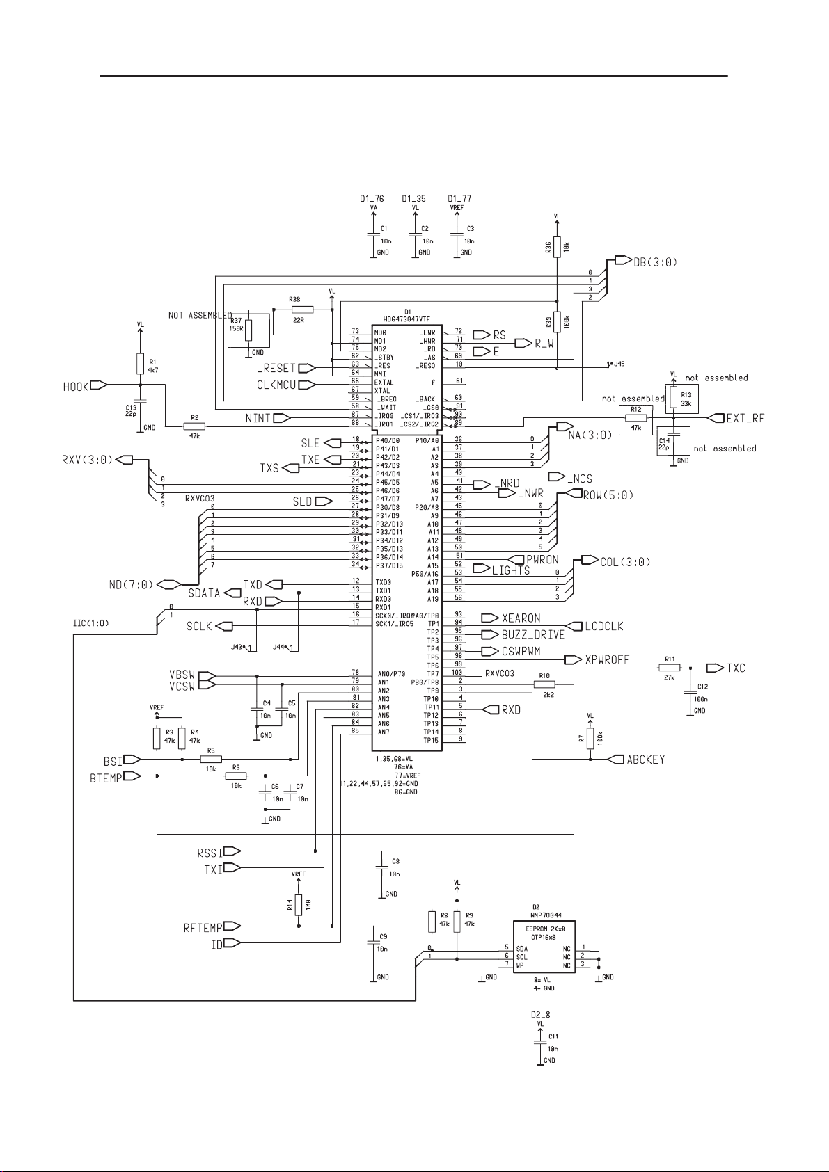
Circuit Diagram of MCU & EEPROM (Version:9.0 Edit: 87) 4 – 14. . .
Circuit Diagram of MCU & EEPROM (Version:11.0 Edit:9.3) 4 – 15. .
Circuit Diagram of Audio (Version:9.0 Edit: 138) 4 – 16. . . . . . . . . . . . .
Circuit Diagram of Audio (Version:11.0 Edit:143) 4 – 17. . . . . . . . . . . .
Circuit Diagram of Power Supply (Version:9.0 Edit:119) 4 – 18. . . . . .
Circuit Diagram of Power Supply (Version:11.0 Edit:127) 4 – 19. . . . .
Circuit Diagram of User Interface (Version:9.0 Edit: 83) 4 – 20. . . . . .
Circuit Diagram of User Interface (Version:11.0 Edit:87) 4 – 21. . . . . .
Block Diagram of RF Section 4 – 22. . . . . . . . . . . . . . . . . . . . . . . . . . . . .
Power Distribution Diagram of RF Section 4 – 23. . . . . . . . . . . . . . . . . .
Circuit Diagram of RF Section (version 9.0) 4 – 24. . . . . . . . . . . . . . . .
Circuit Diagram of RF Section (version 11.0) 4 – 25. . . . . . . . . . . . . . .
Layout Diagrams (version 09) 4 – 26. . . . . . . . . . . . . . . . . . . . . . . . . . . .
Layout Diagrams (version 11) 4 – 27. . . . . . . . . . . . . . . . . . . . . . . . . . . . .
Part List of JRC1 (Issue: 2.10) 4 – 28. . . . . . . . . . . . . . . . . . . . . . . . . . . .
Part List of JRC4 4 – 31. . . . . . . . . . . . . . . . . . . . . . . . . . . . . . . . . . . . . .
Page 4 – 2
Issue2 03/00
Page 3

After Sales
NHA–5
Technical Documentation
RF Block Description
Receiver
The receiver is a dual–conversion superheterodyne using two intermediate frequencies, 45 MHz and 450 kHz.
The RF signal from the duplexer RX port is applied to the RF amplifier.
The amplifier is realized with transistor V700. Amplifier stage input matching is accomplished by C701. R700 and R701 are used for biasing. Output matching is carried out by Z03 and Z04. Components C702 and C703
are used for RF bypassing. The RF amplifier and the IF circuit are connected in series with R702 so that the same supply current is passed
through both stages.
Next the signal is filtered with Z703. The filter is followed by a single balanced diode mixer, realized with Z701, Z711, Z712, C709, C716 and
V701.
RF Block
After the mixer the 45 MHz IF signal is filtered with crystal filter Z702. The
matching between mixer and the filter is realized with L706 and C706.
Next the IF signal is amplified by V703. Input matching is realized with
C714, L702 and L705. The biasing is realized with R713, R714 and R710.
From the amplifier the IF–signal is applied to the second mixer.
The second mixer, the LO buffer transistor, IF amplifier and quadrature
detector are all integrated in the circuit N700. The second LO frequency,
44.55 MHz, is third harmonic off the VCXO frequency. LO signal is realized with tank circuit C719 and L710. After the mixer the 450 kHz IF signal is filtered with ceramic filter Z704. Between the filter and IF amplifier is
a band–pass filter consisting of C728, L709 and C730. The IF amplifier
output signal is phase shifted by resonance circuit C727, C723, R712 and
L704. After this the signal is fed to a quadrature detector.
Signal DAF is low pass filtered by R716 and C734. The DAF, RSSI and
2nd IF signal (450 kHz) are fed to the audio/logic unit.
RX Synthesizer
The first injection frequency is generated by a digital phase locked loop
(PLL). The output frequency of the loop (LO) is obtained from a voltage–
controlled oscillator (VCO) V602. The bandwidth of the PLL can be varied
by dataword programming. The VCO output signal is amplified by transistor V601 and fed to the receiver mixer via Z06. The injection level required by the receiver mixer is about +3 dBm. In addition, the signal is fed
to the dualsynthesizer circuit N650 and via R625 to a LO amplifier which
is realized with V661.
The overall divisor of the chain is selected according to the desired channel.
Issue2 03/00
Page 4 – 3
Page 4

NHA–5
After Sales
RF Block
The internal dividers of N650 are programmed with 17 bits, which are
transferred serially on the SDATA (synthesizer data) line from the processor into an internal shift register also locating in N650. Data transfer is
timed with SCLK clock pulses.
The divided frequency is compared with a highly stable reference frequency by a phase comparator in the PLL circuit (N650). The phase
comparator controls the VCO frequency by means of a d.c. voltage
through the loop filter so as to keep the divided frequency applied to the
phase comparator equal to the fixed reference frequency.
The reference frequency is 30 kHz. This reference frequency is obtained
from The voltage controlled crystal oscillator (VCXO). The oscillator frequency is 14.85 MHz. The VCXO frequency is divided by 495.
RX Loop Filter
Phase comparator output is pin 3. If the VCO frequency is too high, the
output goes low and discharge integrating capacitor C618. After this, the
DC control voltage and the VCO frequency will decrease.
Technical Documentation
If the VCO frequency is too low, the output goes high and charge the integrating capacitor C618. Thereafter the DC control voltage and the VCO
frequency will go up.
Output pulses from the phase detector have to be supplied to the loop filter. The function of the integrator is to convert positive and negative
pulses to DC voltage. The remaining ripple and AC components are filtered in the lowpass filter. The integrator comprises components R610,
C619, C624 and C618. The lowpass filter consists of R608 and C616.
RX VCO
The VCO is a Clapp type oscillator. The oscillator’s resonant frequency is
determined by the circuitry Z600, C604, V603,C601, C614, C611, C612
and C613. The center frequency of the VCO is adjusted by changing
amount of constant current generated by V100 in BB section. The VCO
signal is amplified by buffer amplifier V601. This amplifier produces a level of –5 dBm to the synthesizer N650 and amplifier V661 in TX synthesizer via R625. The same buffer V601 produces +3 dBm level to the first
mixer via Z06.
TX Synthesizer
Page 4 – 4
The transmitter synthesizer generates a frequency modulated transmitter
signal for the transmitter section.
The TX offset synthesizer consists of a 90 MHz PLL circuit, passive loop
filter and a 90 MHz VCO equipped with a chip coil resonator. The bandwidth of the PLL can be varied by dataword programming. Modulation is
brought to the VCO.
Issue2 03/00
Page 5

After Sales
NHA–5
Technical Documentation
The TX signal is obtained by mixing the signals of offset synthesizer and
RX synthesizer with a single balanced diode mixer. From the mixer the
–10 dBm level is fed to the amplifier. The TX signal is filtered with a SAW
filter before inputting it to the transmitter.
TX VCO
The VCO is a Clapp type oscillator. The oscillator’s resonance frequency
is determined by the circuitry L651, C659, V659, C663, C630, C631 and
C675. The center frequency of the resonance circuit is not adjustable (By
increasing or decreasing the capacitor C659 the resonance frequency
can be changed). The VCO signal is amplified by V657 and fed to the
prescaler and to the mixer.
TX Loop Filter
Output pulses from the phase detector N650 pin 17 have to be supplied
to the loop filter. The integrator, which is constituted of R674, C680 and
C683, converts positive and negative pulses to d.c. voltage. The remaining ripple is filtered in the low–pass filter accomplished by R672 and
C665.
RF Block
Transmitter
The transmitter is realized with four discrete transistors. The modulated
RF signal from the TX synthesizer is applied to the input transistor V660
of the transmitter. V660 amplifies the signal for the power control stage
V803, which is biased to B–class. The power level is controlled by the collector voltage of V803. Transistors V804 and V805 are biased to C–class
and amplify the RF signal to the desired output power level. The amplified
RF signal is fed through a low–pass filter to the duplex filter. The harmonics of the transmitter are reduced by the duplex filter. A voltage proportional to the output power is rectified from a directional coupler by d.c.
biased Schottky diode V801. This rectified voltage is fed to a differential
amplifier which consists of double transistor V809. There is a negative
feedback from the rectified voltage to the bias voltage of diode V801 consisting of transistor V810 and associated components. The purpose of arranging the feedback is to suppress the rectified voltage to a range below
3 volts. The reference voltage is filtered from the PWM signal TXC by
R814 and C826. The differential amplifier adjusts the collector voltage of
the transistor V803 so that the reference voltage and the voltage proportional to the output power are equal. The transmitter is switched on when
TXE goes high (logic 1), which enables the transmitter power control circuit by transistor V808 and the first stage of the transmitter. When the
transmitter is inactive (TXE low) the RF level from the transmitter is reduced below –60 dBm.
The rectified voltage, which is proportional to the power output signal, is
fed along TXI line through R820 to the BB–unit. This TXI line (TX power
on Indicator) is used to avoid false transmission.
Issue2 03/00
Page 4 – 5
Page 6

NHA–5
After Sales
RF Block
Regulators
Transistors V901 and V902 form a voltage regulator for RF parts. It is
realized with discrete transistors because the output noise has to be very
low. The 3.3 V reference voltage (VREF) comes from the logic module.
This regulated voltage goes directly to RX part and also to RX synthesizer. TX synthesizer get it’s supply voltage via a switch. The switch is realized with transistors V651 and V654.It is controlled over digital line TXS
from the logic module.
Technical Documentation
Page 4 – 6
Issue2 03/00
Page 7
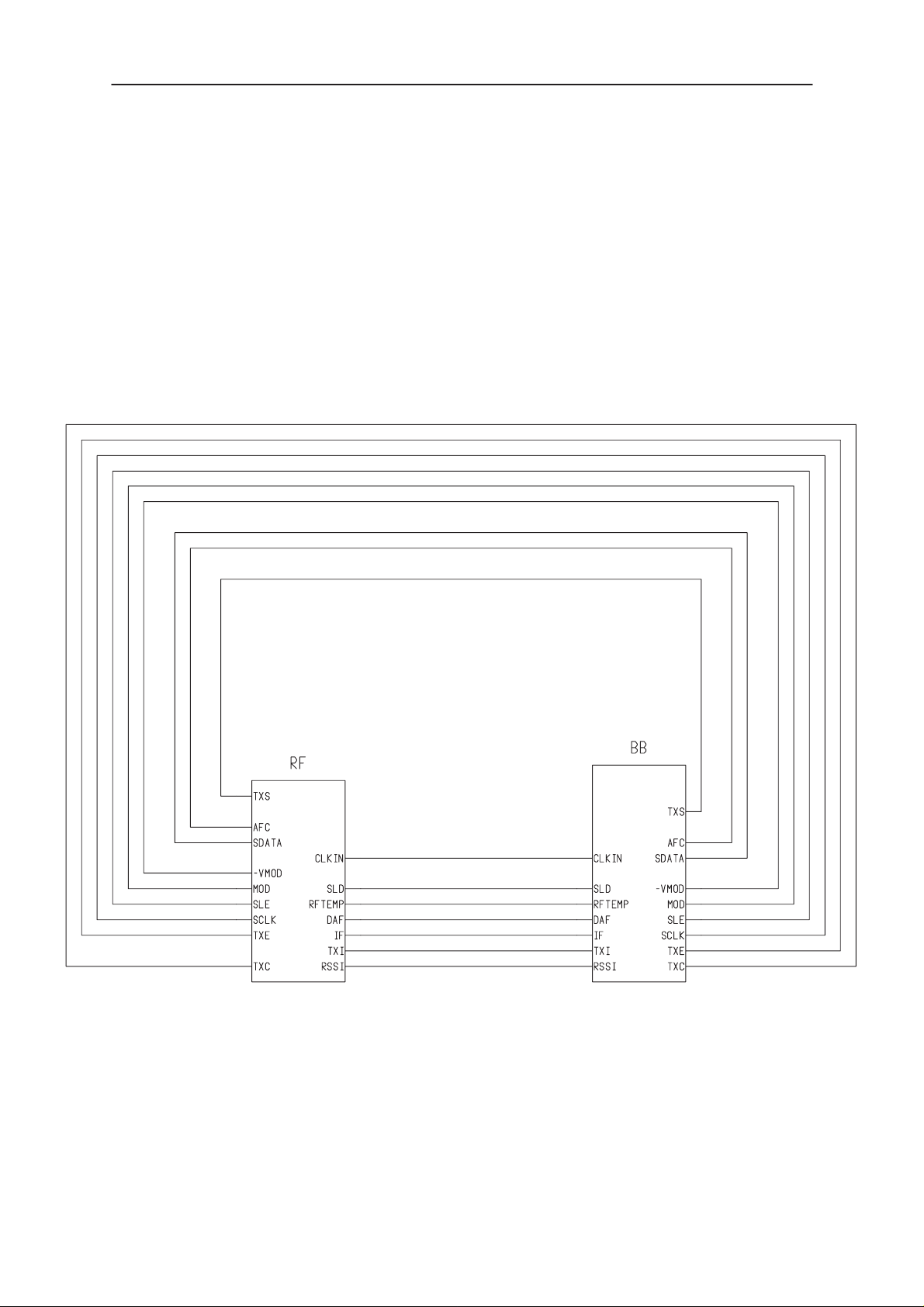
After Sales
NHA–5
Technical Documentation
RF Block
Connections between RF and BB Sections (Version: 4.0 Edit: 66)
Issue2 03/00
Page 4 – 7
Page 8
NHA–5
After Sales
RF Block
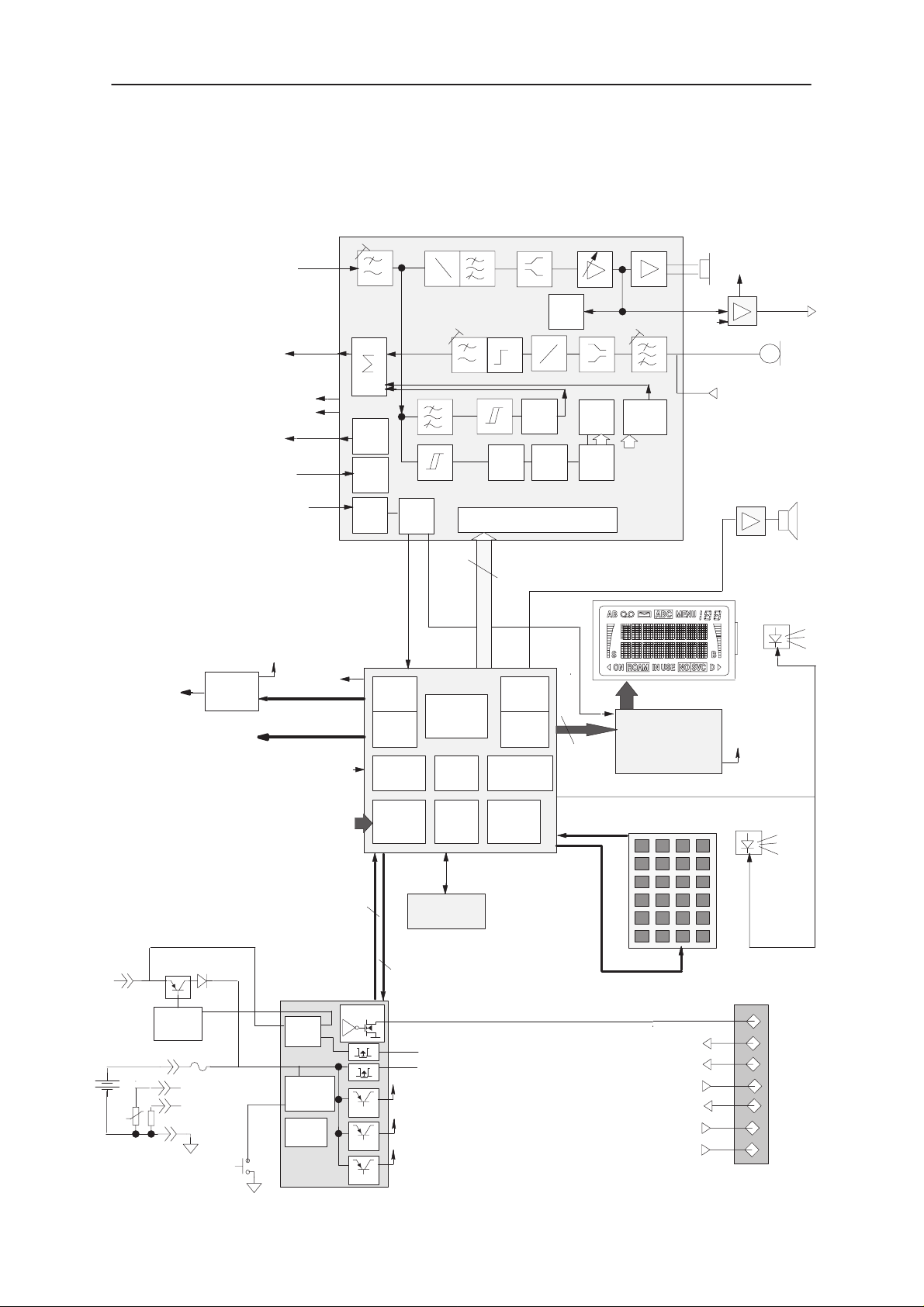
Block Diagram of Baseband
NASTA
DAF
D/A
IF
CTR
SPEECH
DATA/ST
CLK
DIV
SAT
DATA
SYNBIAS
RXBIAS
14.85 MHz
MOD
AFC
IF
CTR
CLK
GEN
SAT
DET
MAN
DPLL
DEC
MCU INTERFACE
HF
DET
Technical Documentation
EARPHONE
EAR
VBAT
XEARON
MIC
MICROPHONE
VOTE
SMUX
SMUX
DATA/
ST
ENCODE
XMIC
XEAR
BUZZER
VC
4.8V
NTC
Battery
pack
–VMOD
TXE,TXS,TXC
SLE,SDATA,SCLK
Charge
switch
control
VBAT
BTEMP
BSI
ON/OFF
VCO
NEG VOLT
TRIM
–VLCD
XEARON
RXV(3:0)
RF CONTROLS
HOOK, EXT_RF
Charger
det,crl
VB det
RESET
PWR ON
WDOG
MUUMI
VBSW
VCSW
BTEMP
BSI
RSSI
TXI
RFTEMP
XMIC/ID
RESET,PWRON
MBUS
2.4MHz
WDOG
TIMER
ITU
16 BIT
TIMERS
INTERRUPT
CONTROL
A/D
10 BIT
8 CH
2 kbytes
TXD,XPWROFF
VL=3.3V
VA=3.3V
VREF=3.3V
H8/3047
H8/300
CPU
ROM
96K
RAM
4K
SCL,SDA
EEPROM
VCSW
VBSW
ND0–7,NA0–3
_NCS,_WR,_RD
_NINT
DMA
REFRESH
CONTRL
TPC,
TIMING
PATTERN CRL
SCI
SERIAL
IFCE
2 CHAN
80 kHz
RS,R/W,E,
DB0–3
LIGHTS
ROW0–5
BUZZ_DRIVE
COM1–7,COM9–15,COMMK
SEG1–60
LCD–
CONTROLLER
KEYBOARD
COL0–3
HOOK
EXT_RF
XEAR
XMIC
ACCESSORY
CONNECTOR
–VLCDout
MBUS
HOOK
EXT_RF
XEAR
XMIC
BENA
V_OUT
Page 4 – 8
Issue2 03/00
Page 9
Issue2 03/00
MIC
BIMIC
CMIC
XMIC
50
2.4
REF
14.85 MHz>500 pp
CLKIN
CLKOUT
IF
(450 kHz)
MICAM
DTMF GEN
GND GEN
OSC
IFAMP
REF GEN
CLKGEN
TXMUX TXATT MICTRI TXBP
XCLR
TMODE
CLKLCD CLKMCU
TSEL
CLOCKDIV
MCS1&2
IFCNTR
MANDEC
Nom–dev
50 71
ATTO
COMI
CWCI
COMO
COMPR LIM1
sideari
BCH
INT
CLOCKS
VOTE
TIMER
EMPI
SMUX
CORR
100
EMPO LPIN
PREEM LIM2 TXLP TXTRI
MANEN
STATUS BITS
TR
Par/Ser
SYNBIAS
CONTROL BITS
RXBIAS
TOUT
CREG
Max–dev
aloop
DATA
GEN
SAT
GEN
ST
GEN
SUM
TXTRI
SATFIL
HFBP
SATCOMP
DATAC
CAMPBO
Extended
210
Data–dev
WTRFIL
ATST
ATOUT
D/St 1640 pp
Sat 410/435 pp
210
MOD
loop
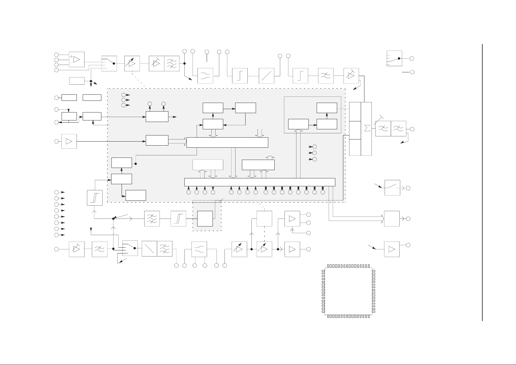
Block Diagram of NASTA
After Sales
Technical Documentation
VDD1
VDD2
VSS2
VDA1
VSA1
VDA2
VSA2
VSS1
DAF
50
D 398 pp
Sat 99/100 pp
Page 4 – 9
DATAC
D 792 pp
dtmf
RXTRI RXAAF
100
DPLL
loop
DATVAL
RXMUX
aloop
XCSXRDXWRXINT A0 A1 A2 A3 D0 D1 D2 D3 D4 D5 D6 D7
SATFIL,6kHz SATCOMP SATDET
360
RXFIL
71
FILO
EXP VOL
EAMPBO
EXPI
EWCI
EXPO
4
50
VOLI
INTERFACE
HF
CONTR
RXATT ACC
Level: AMPS/TACS (mVrms)
All levels: (mV)
( ) : Not use now
EAR
64 pins Tqfp
50
EARP
50
EARM
EVGND
XEAR
50
VDD1
XRD
XCS
A3
A2
A1
A0
D7
D6
D5
D4
D3
D2
D1
D0
VDD2
1 2 3 4 5 6 7 8 9 1011 1213141516
63CLKMCU
64XWR
18 XCLR
17 TOUT
61CLKIN
62CLKLCD
20 TSEL
19 TMODE
59ATOUT
60CLKOUT
22 SYNBIAS
21 XINT
57VSS1
58BUZZ
NASTA
24 IF
23 RXBIAS
56VSA1
25 VSS2
55MOD
26 VSA2
sideari
SIDEAR
AFC
dtmf
D/A
8 bit
BUZZ DRIV
DACO
BUZZ
(1500 pp)
(3000 pp)
49COMI
50COMO
51EMPI
52EMPO
53LPIN
54ATST
48474645444342414039383736353433
VDA1
ATTO
XMIC
CMIC
BIMIC
MIC
REF
SIDEAR
DACO
CWCI
EARP
EARM
EVGND
XEAR
VOLI
VDA2
32 EXPO
31 EWCI
30 EAMPBO
29 EXPI
28 FILO
27 DAF
RF Block
NHA–5
Page 10
NHA–5
After Sales
RF Block
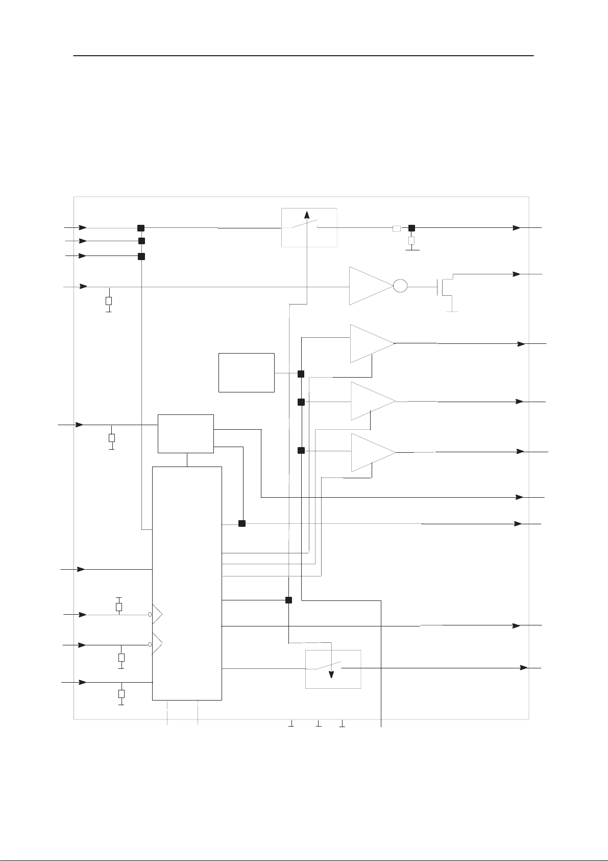
Block Diagram of MUUMI
VBAT1
1
VBAT2
22
VBAT3
5
M2BUSIN
11
760k
Technical Documentation
70k
40k
VBATSW
M2BUSOUT
17
12
VL
23
15
21
13
14
3
PWM
VCHAR
PWRONX
PWROFFX
TEST
VBAT
760k
32k
760k
760k
CHARGER
CTRL
LOGIC
LOW VBAT
& CHARGER
DETECT
PWR ON/OFF
&
RESET LOGIC
Creset
20
16
Coff
BANDGAP
REF
VL_ENA
VA_ENA
VREF_ENA
VSW_ENA
VCHAR
24
GND1
GND2
19
GND3
7
VA
2
VREF
CHRGSW
PURX
PWRONXBUFF
VCHARSW
Cref
4
8
10
9
18
6
Page 4 – 10
Issue2 03/00
Page 11
After Sales
NHA–5
Technical Documentation
Block Diagram of Baseband Power Distribution
VBVC
VL
MUUMI
VA
NASTA
Microcontroller
VREF
LCD
controller
EEPROM
RF Block
Issue2 03/00
Page 4 – 11
Page 12
NHA–5
After Sales
RF Block
Technical Documentation
Circuit Diagram of MCU & EEPROM (Version:4.0 Edit: 113)
Page 4 – 12
Issue2 03/00
Page 13

After Sales
NHA–5
Technical Documentation
Circuit Diagram of Power Supply (Version:4.0 Edit:135)
RF Block
Issue2 03/00
Page 4 – 13
Page 14

NHA–5
After Sales
RF Block
Block Diagram of RF Section
Technical Documentation
Page 4 – 14
Issue2 03/00
Page 15

After Sales
NHA–5
Technical Documentation
Power Distribution Diagram of RF Section
RF Block
Issue2 03/00
Page 4 – 15
Page 16

NHA–5
After Sales
RF Block
Technical Documentation
Circuit Diagram of Baseband Module (Version: 4.0 Edit: 145)
Page 4 – 16
Issue2 03/00
Page 17

After Sales
NHA–5
Technical Documentation
Circuit Diagram of RF Section (Version: 4.0 Edit: 62)
RF Block
Issue2 03/00
Page 4 – 17
Page 18

NHA–5
After Sales
RF Block
Technical Documentation
Circuit Diagram of Audio Section (Version 4.0 Edit 165)
Page 4 – 18
Issue2 03/00
Page 19

After Sales
NHA–5
Technical Documentation
RF Block
Circuit Diagram of Keyboard Section (Version 4.0 Edit 97)
Issue2 03/00
Page 4 – 19
Page 20

NHA–5
After Sales
RF Block
Layout Diagrams (Version 04)
Technical Documentation
Page 4 – 20
Issue2 03/00
Page 21

After Sales
NHA–5
Technical Documentation
RF Block
Part List of JRC1 (Issue: 2.10) Code: 0200871
ITEM CODE DESCRIPTION VALUE TYPE
R001 1430770 Chip resistor 4.7 k 5 % 0.063 W 0402
R002 1430796 Chip resistor 47 k 5 % 0.063 W 0402
R003 1430796 Chip resistor 47 k 5 % 0.063 W 0402
R004 1430796 Chip resistor 47 k 5 % 0.063 W 0402
R005 1430778 Chip resistor 10 k 5 % 0.063 W 0402
R006 1430778 Chip resistor 10 k 5 % 0.063 W 0402
R007 1430804 Chip resistor 100 k 5 % 0.063 W 0402
R008 1430796 Chip resistor 47 k 5 % 0.063 W 0402
R009 1430796 Chip resistor 47 k 5 % 0.063 W 0402
R010 1430762 Chip resistor 2.2 k 5 % 0.063 W 0402
R011 1430790 Chip resistor 27 k 5 % 0.063 W 0402
R014 1430830 Chip resistor 1.0 M 5 % 0.063 W 0402
R015 1430796 Chip resistor 47 k 5 % 0.063 W 0402
R016 1430758 Chip resistor 1.5 k 5 % 0.063 W 0402
R017 1430740 Chip resistor 330 5 % 0.063 W 0402
R018 1430764 Chip resistor 3.3 k 5 % 0.063 W 0402
R019 1430788 Chip resistor 22 k 5 % 0.063 W 0402
R020 1430770 Chip resistor 4.7 k 5 % 0.063 W 0402
R021 1430778 Chip resistor 10 k 5 % 0.063 W 0402
R022 1430780 Chip resistor 12 k 5 % 0.063 W 0402
R023 1430786 Chip resistor 18 k 5 % 0.063 W 0402
R024 1430778 Chip resistor 10 k 5 % 0.063 W 0402
R025 1430730 Chip resistor 150 5 % 0.063 W 0402
R026 1430804 Chip resistor 100 k 5 % 0.063 W 0402
R027 1430786 Chip resistor 18 k 5 % 0.063 W 0402
R028 1430770 Chip resistor 4.7 k 5 % 0.063 W 0402
R029 1430770 Chip resistor 4.7 k 5 % 0.063 W 0402
R030 1430734 Chip resistor 220 5 % 0.063 W 0402
R031 1430754 Chip resistor 1.0 k 5 % 0.063 W 0402
R032 1430754 Chip resistor 1.0 k 5 % 0.063 W 0402
R033 1430754 Chip resistor 1.0 k 5 % 0.063 W 0402
R034 1430754 Chip resistor 1.0 k 5 % 0.063 W 0402
R035 1430804 Chip resistor 100 k 5 % 0.063 W 0402
R038 1430710 Chip resistor 22 5 % 0.063 W 0402
R039 1430804 Chip resistor 100 k 5 % 0.063 W 0402
R040 1430762 Chip resistor 2.2 k 5 % 0.063 W 0402
R041 1430762 Chip resistor 2.2 k 5 % 0.063 W 0402
R042 1430710 Chip resistor 22 5 % 0.063 W 0402
R043 1430710 Chip resistor 22 5 % 0.063 W 0402
R044 1430754 Chip resistor 1.0 k 5 % 0.063 W 0402
R050 1430792 Chip resistor 33 k 5 % 0.063 W 0402
R051 1430762 Chip resistor 2.2 k 5 % 0.063 W 0402
R052 1430778 Chip resistor 10 k 5 % 0.063 W 0402
Issue2 03/00
Page 4 – 21
Page 22

NHA–5
After Sales
RF Block
R053 1430762 Chip resistor 2.2 k 5 % 0.063 W 0402
R054 1430804 Chip resistor 100 k 5 % 0.063 W 0402
R056 1430764 Chip resistor 3.3 k 5 % 0.063 W 0402
R058 1430700 Chip resistor 10 5 % 0.063 W 0402
R059 1430700 Chip resistor 10 5 % 0.063 W 0402
R060 1430778 Chip resistor 10 k 5 % 0.063 W 0402
R062 1430788 Chip resistor 22 k 5 % 0.063 W 0402
R063 1430710 Chip resistor 22 5 % 0.063 W 0402
R064 1430700 Chip resistor 10 5 % 0.063 W 0402
R065 1430744 Chip resistor 470 5 % 0.063 W 0402
R066 1430718 Chip resistor 47 5 % 0.063 W 0402
R067 1430744 Chip resistor 470 5 % 0.063 W 0402
R071 1430804 Chip resistor 100 k 5 % 0.063 W 0402
R072 1430804 Chip resistor 100 k 5 % 0.063 W 0402
R073 1430804 Chip resistor 100 k 5 % 0.063 W 0402
R074 1430734 Chip resistor 220 5 % 0.063 W 0402
R100 1430812 Chip resistor 220 k 5 % 0.063 W 0402
R101 1430816 Chip resistor 330 k 5 % 0.063 W 0402
R102 1430822 Chip resistor 560 k 5 % 0.063 W 0402
R103 1430830 Chip resistor 1.0 M 5 % 0.063 W 0402
R104 1430826 Chip resistor 680 k 5 % 0.063 W 0402
R106 1430808 Chip resistor 150 k 5 % 0.063 W 0402
R107 1430790 Chip resistor 27 k 5 % 0.063 W 0402
R108 1411194 Chip jumper 1206
R600 1430726 Chip resistor 100 5 % 0.063 W 0402
R604 1430710 Chip resistor 22 5 % 0.063 W 0402
R605 1430832 Chip resistor 2.7 k 5 % 0.063 W 0402
R606 1430724 Chip resistor 82 5 % 0.063 W 0402
R607 1430726 Chip resistor 100 5 % 0.063 W 0402
R608 1430776 Chip resistor 8.2 k 5 % 0.063 W 0402
R609 1430720 Chip resistor 56 5 % 0.063 W 0402
R610 1430762 Chip resistor 2.2 k 5 % 0.063 W 0402
R611 1430762 Chip resistor 2.2 k 5 % 0.063 W 0402
R612 1430764 Chip resistor 3.3 k 5 % 0.063 W 0402
R613 1430728 Chip resistor 120 5 % 0.063 W 0402
R614 1430718 Chip resistor 47 5 % 0.063 W 0402
R615 1430798 Chip resistor 56 k 5 % 0.063 W 0402
R616 1430700 Chip resistor 10 5 % 0.063 W 0402
R617 1430746 Chip resistor 560 5 % 0.063 W 0402
R619 1430774 Chip resistor 6.8 k 5 % 0.063 W 0402
R620 1430796 Chip resistor 47 k 5 % 0.063 W 0402
R621 1430778 Chip resistor 10 k 5 % 0.063 W 0402
R622 1430778 Chip resistor 10 k 5 % 0.063 W 0402
R623 1430778 Chip resistor 10 k 5 % 0.063 W 0402
R624 1430718 Chip resistor 47 5 % 0.063 W 0402
R625 1430722 Chip resistor 68 5 % 0.063 W 0402
R626 1430832 Chip resistor 2.7 k 5 % 0.063 W 0402
Technical Documentation
Page 4 – 22
Issue2 03/00
Page 23

After Sales
NHA–5
Technical Documentation
R627 1430762 Chip resistor 2.2 k 5 % 0.063 W 0402
R628 1430700 Chip resistor 10 5 % 0.063 W 0402
R629 1430832 Chip resistor 2.7 k 5 % 0.063 W 0402
R630 1430832 Chip resistor 2.7 k 5 % 0.063 W 0402
R631 1430710 Chip resistor 22 5 % 0.063 W 0402
R632 1430804 Chip resistor 100 k 5 % 0.063 W 0402
R633 1430740 Chip resistor 330 5 % 0.063 W 0402
R635 1430714 Chip resistor 33 5 % 0.063 W 0402
R636 1430754 Chip resistor 1.0 k 5 % 0.063 W 0402
R637 1430714 Chip resistor 33 5 % 0.063 W 0402
R639 1430742 Chip resistor 390 5 % 0.063 W 0402
R640 1430778 Chip resistor 10 k 5 % 0.063 W 0402
R641 1430726 Chip resistor 100 5 % 0.063 W 0402
R645 1430700 Chip resistor 10 5 % 0.063 W 0402
R646 1430730 Chip resistor 150 5 % 0.063 W 0402
R647 1430734 Chip resistor 220 5 % 0.063 W 0402
R652 1430778 Chip resistor 10 k 5 % 0.063 W 0402
R653 1430764 Chip resistor 3.3 k 5 % 0.063 W 0402
R654 1430804 Chip resistor 100 k 5 % 0.063 W 0402
R656 1430762 Chip resistor 2.2 k 5 % 0.063 W 0402
R659 1430754 Chip resistor 1.0 k 5 % 0.063 W 0402
R660 1430700 Chip resistor 10 5 % 0.063 W 0402
R663 1430722 Chip resistor 68 5 % 0.063 W 0402
R664 1430754 Chip resistor 1.0 k 5 % 0.063 W 0402
R667 1430748 Chip resistor 680 5 % 0.063 W 0402
R668 1430718 Chip resistor 47 5 % 0.063 W 0402
R669 1430778 Chip resistor 10 k 5 % 0.063 W 0402
R670 1430742 Chip resistor 390 5 % 0.063 W 0402
R671 1430754 Chip resistor 1.0 k 5 % 0.063 W 0402
R672 1430764 Chip resistor 3.3 k 5 % 0.063 W 0402
R673 1430764 Chip resistor 3.3 k 5 % 0.063 W 0402
R674 1430762 Chip resistor 2.2 k 5 % 0.063 W 0402
R675 1430700 Chip resistor 10 5 % 0.063 W 0402
R681 1430726 Chip resistor 100 5 % 0.063 W 0402
R683 1430802 Chip resistor 82 k 5 % 0.063 W 0402
R700 1430778 Chip resistor 10 k 5 % 0.063 W 0402
R701 1430754 Chip resistor 1.0 k 5 % 0.063 W 0402
R702 1430700 Chip resistor 10 5 % 0.063 W 0402
R703 1430762 Chip resistor 2.2 k 5 % 0.063 W 0402
R705 1430726 Chip resistor 100 5 % 0.063 W 0402
R710 1430774 Chip resistor 6.8 k 5 % 0.063 W 0402
R712 1430764 Chip resistor 3.3 k 5 % 0.063 W 0402
R713 1430784 Chip resistor 15 k 5 % 0.063 W 0402
R714 1430754 Chip resistor 1.0 k 5 % 0.063 W 0402
R715 1430758 Chip resistor 1.5 k 5 % 0.063 W 0402
R716 1430762 Chip resistor 2.2 k 5 % 0.063 W 0402
R717 1430700 Chip resistor 10 5 % 0.063 W 0402
RF Block
Issue2 03/00
Page 4 – 23
Page 24

NHA–5
After Sales
RF Block
R718 1430700 Chip resistor 10 5 % 0.063 W 0402
R721 1430724 Chip resistor 82 5 % 0.063 W 0402
R801 1430724 Chip resistor 82 5 % 0.063 W 0402
R804 1430734 Chip resistor 220 5 % 0.063 W 0402
R805 1430762 Chip resistor 2.2 k 5 % 0.063 W 0402
R806 1430746 Chip resistor 560 5 % 0.063 W 0402
R807 1430700 Chip resistor 10 5 % 0.063 W 0402
R808 1430718 Chip resistor 47 5 % 0.063 W 0402
R809 1430700 Chip resistor 10 5 % 0.063 W 0402
R810 1430718 Chip resistor 47 5 % 0.063 W 0402
R811 1430700 Chip resistor 10 5 % 0.063 W 0402
R813 1430700 Chip resistor 10 5 % 0.063 W 0402
R814 1430778 Chip resistor 10 k 5 % 0.063 W 0402
R815 1430778 Chip resistor 10 k 5 % 0.063 W 0402
R816 1430792 Chip resistor 33 k 5 % 0.063 W 0402
R817 1430754 Chip resistor 1.0 k 5 % 0.063 W 0402
R818 1430792 Chip resistor 33 k 5 % 0.063 W 0402
R819 1430770 Chip resistor 4.7 k 5 % 0.063 W 0402
R820 1430792 Chip resistor 33 k 5 % 0.063 W 0402
R821 1430772 Chip resistor 5.6 k 5 % 0.063 W 0402
R823 1430804 Chip resistor 100 k 5 % 0.063 W 0402
R824 1430770 Chip resistor 4.7 k 5 % 0.063 W 0402
R825 1430710 Chip resistor 22 5 % 0.063 W 0402
R901 1430762 Chip resistor 2.2 k 5 % 0.063 W 0402
R902 1430788 Chip resistor 22 k 5 % 0.063 W 0402
R903 1430754 Chip resistor 1.0 k 5 % 0.063 W 0402
R904 1430778 Chip resistor 10 k 5 % 0.063 W 0402
R906 1430778 Chip resistor 10 k 5 % 0.063 W 0402
R907 1430778 Chip resistor 10 k 5 % 0.063 W 0402
C001 2320107 Ceramic cap. 10 n 5 % 50 V 0603
C002 2320107 Ceramic cap. 10 n 5 % 50 V 0603
C003 2320107 Ceramic cap. 10 n 5 % 50 V 0603
C004 2320107 Ceramic cap. 10 n 5 % 50 V 0603
C005 2320107 Ceramic cap. 10 n 5 % 50 V 0603
C006 2320107 Ceramic cap. 10 n 5 % 50 V 0603
C007 2320107 Ceramic cap. 10 n 5 % 50 V 0603
C008 2320107 Ceramic cap. 10 n 5 % 50 V 0603
C009 2320107 Ceramic cap. 10 n 5 % 50 V 0603
C011 2320107 Ceramic cap. 10 n 5 % 50 V 0603
C012 2310784 Ceramic cap. 100 n 10 % 25 V 0805
C013 2320544 Ceramic cap. 22 p 5 % 50 V 0402
C015 2320107 Ceramic cap. 10 n 5 % 50 V 0603
C016 2320107 Ceramic cap. 10 n 5 % 50 V 0603
C017 2610100 Tantalum cap. 1 u 20 % 10 V 2.0x1.3x1.2
C018 2604456 Tantalum cap. 4.7 u 20 % 16 V 4.7x2.6x2.1
C019 2320107 Ceramic cap. 10 n 5 % 50 V 0603
C020 2320107 Ceramic cap. 10 n 5 % 50 V 0603
Technical Documentation
Page 4 – 24
Issue2 03/00
Page 25

After Sales
NHA–5
Technical Documentation
C021 2320107 Ceramic cap. 10 n 5 % 50 V 0603
C022 2604199 Tantalum cap. 2.2 u 20 % 3.2x1.6x1.6
C023 2604199 Tantalum cap. 2.2 u 20 % 3.2x1.6x1.6
C024 2604199 Tantalum cap. 2.2 u 20 % 3.2x1.6x1.6
C025 2320576 Ceramic cap. 470 p 5 % 50 V 0402
C030 2320546 Ceramic cap. 27 p 5 % 50 V 0402
C050 2310791 Ceramic cap. 33 n 20 % 50 V 0805
C051 2310791 Ceramic cap. 33 n 20 % 50 V 0805
C052 2310791 Ceramic cap. 33 n 20 % 50 V 0805
C053 2310791 Ceramic cap. 33 n 20 % 50 V 0805
C054 2310791 Ceramic cap. 33 n 20 % 50 V 0805
C055 2310784 Ceramic cap. 100 n 10 % 25 V 0805
C056 2310791 Ceramic cap. 33 n 20 % 50 V 0805
C057 2310777 Ceramic cap. 22 n 20 % 50 V 0805
C058 2320546 Ceramic cap. 27 p 5 % 50 V 0402
C059 2320107 Ceramic cap. 10 n 5 % 50 V 0603
C060 2320107 Ceramic cap. 10 n 5 % 50 V 0603
C062 2310791 Ceramic cap. 33 n 20 % 50 V 0805
C063 2310791 Ceramic cap. 33 n 20 % 50 V 0805
C064 2310791 Ceramic cap. 33 n 20 % 50 V 0805
C066 2312410 Ceramic cap. 1.0 u 10 % 16 V 1206
C068 2320107 Ceramic cap. 10 n 5 % 50 V 0603
C069 2320592 Ceramic cap. 2.2 n 5 % 50 V 0402
C070 2312410 Ceramic cap. 1.0 u 10 % 16 V 1206
C071 2320584 Ceramic cap. 1.0 n 5 % 50 V 0402
C072 2320546 Ceramic cap. 27 p 5 % 50 V 0402
C076 2310784 Ceramic cap. 100 n 10 % 25 V 0805
C077 2320584 Ceramic cap. 1.0 n 5 % 50 V 0402
C078 2320584 Ceramic cap. 1.0 n 5 % 50 V 0402
C600 2320520 Ceramic cap. 2.2 p 0.25 % 50 V 0402
C601 2320526 Ceramic cap. 3.9 p 0.25 % 50 V 0402
C602 2320524 Ceramic cap. 3.3 p 0.25 % 50 V 0402
C603 2320560 Ceramic cap. 100 p 5 % 50 V 0402
C604 2320546 Ceramic cap. 27 p 5 % 50 V 0402
C605 2611668 Tantalum cap. 4.7 u 20 % 10 V 3.2x1.6x1.6
C606 2320602 Ceramic cap. 4.7 p 0.25 % 50 V 0402
C607 2611668 Tantalum cap. 4.7 u 20 % 10 V 3.2x1.6x1.6
C608 2320596 Ceramic cap. 3.3 n 5 % 50 V 0402
C609 2604199 Tantalum cap. 2.2 u 20 % 3.2x1.6x1.6
C610 2320596 Ceramic cap. 3.3 n 5 % 50 V 0402
C611 2320538 Ceramic cap. 12 p 5 % 50 V 0402
C612 2320524 Ceramic cap. 3.3 p 0.25 % 50 V 0402
C613 2320520 Ceramic cap. 2.2 p 0.25 % 50 V 0402
C614 2320554 Ceramic cap. 56 p 5 % 50 V 0402
C616 2310769 Ceramic cap. 15 n 20 % 50 V 0805
C617 2320546 Ceramic cap. 27 p 5 % 50 V 0402
C618 2604209 Tantalum cap. 1.0 u 20 % 16 V 3.2x1.6x1.6
RF Block
Issue2 03/00
Page 4 – 25
Page 26

NHA–5
After Sales
RF Block
C619 2310791 Ceramic cap. 33 n 20 % 50 V 0805
C620 2320584 Ceramic cap. 1.0 n 5 % 50 V 0402
C621 2320596 Ceramic cap. 3.3 n 5 % 50 V 0402
C622 2320544 Ceramic cap. 22 p 5 % 50 V 0402
C623 2604199 Tantalum cap. 2.2 u 20 % 3.2x1.6x1.6
C624 2310791 Ceramic cap. 33 n 20 % 50 V 0805
C625 2320546 Ceramic cap. 27 p 5 % 50 V 0402
C627 2611668 Tantalum cap. 4.7 u 20 % 10 V 3.2x1.6x1.6
C628 2320107 Ceramic cap. 10 n 5 % 50 V 0603
C629 2320546 Ceramic cap. 27 p 5 % 50 V 0402
C630 2320554 Ceramic cap. 56 p 5 % 50 V 0402
C631 2320556 Ceramic cap. 68 p 5 % 50 V 0402
C632 2604209 Tantalum cap. 1.0 u 20 % 16 V 3.2x1.6x1.6
C633 2320584 Ceramic cap. 1.0 n 5 % 50 V 0402
C634 2320584 Ceramic cap. 1.0 n 5 % 50 V 0402
C635 2320534 Ceramic cap. 8.2 p 0.25 % 50 V 0402
C636 2320546 Ceramic cap. 27 p 5 % 50 V 0402
C637 2320584 Ceramic cap. 1.0 n 5 % 50 V 0402
C638 2320596 Ceramic cap. 3.3 n 5 % 50 V 0402
C639 2320548 Ceramic cap. 33 p 5 % 50 V 0402
C640 2320548 Ceramic cap. 33 p 5 % 50 V 0402
C641 2320546 Ceramic cap. 27 p 5 % 50 V 0402
C642 2320602 Ceramic cap. 4.7 p 0.25 % 50 V 0402
C643 2320546 Ceramic cap. 27 p 5 % 50 V 0402
C644 2320596 Ceramic cap. 3.3 n 5 % 50 V 0402
C654 2320107 Ceramic cap. 10 n 5 % 50 V 0603
C655 2604209 Tantalum cap. 1.0 u 20 % 16 V 3.2x1.6x1.6
C656 2320546 Ceramic cap. 27 p 5 % 50 V 0402
C657 2320596 Ceramic cap. 3.3 n 5 % 50 V 0402
C658 2320584 Ceramic cap. 1.0 n 5 % 50 V 0402
C659 2320556 Ceramic cap. 68 p 5 % 50 V 0402
C660 2320546 Ceramic cap. 27 p 5 % 50 V 0402
C662 2320602 Ceramic cap. 4.7 p 0.25 % 50 V 0402
C663 2320576 Ceramic cap. 470 p 5 % 50 V 0402
C665 2310780 Ceramic cap. 68 n 10 % 25 V 0805
C669 2320596 Ceramic cap. 3.3 n 5 % 50 V 0402
C670 2611668 Tantalum cap. 4.7 u 20 % 10 V 3.2x1.6x1.6
C671 2320548 Ceramic cap. 33 p 5 % 50 V 0402
C675 2320548 Ceramic cap. 33 p 5 % 50 V 0402
C676 2320546 Ceramic cap. 27 p 5 % 50 V 0402
C677 2320524 Ceramic cap. 3.3 p 0.25 % 50 V 0402
C678 2320526 Ceramic cap. 3.9 p 0.25 % 50 V 0402
C679 2320560 Ceramic cap. 100 p 5 % 50 V 0402
C680 2610016 Tantalum cap. 0.47 u 10 % 25 V 3.2x1.6x1.6
C681 2320552 Ceramic cap. 47 p 5 % 50 V 0402
C682 2320552 Ceramic cap. 47 p 5 % 50 V 0402
C683 2611668 Tantalum cap. 4.7 u 20 % 10 V 3.2x1.6x1.6
Technical Documentation
Page 4 – 26
Issue2 03/00
Page 27

After Sales
NHA–5
Technical Documentation
C686 2320560 Ceramic cap. 100 p 5 % 50 V 0402
C690 2604209 Tantalum cap. 1.0 u 20 % 16 V 3.2x1.6x1.6
C691 2320548 Ceramic cap. 33 p 5 % 50 V 0402
C701 2320546 Ceramic cap. 27 p 5 % 50 V 0402
C702 2320560 Ceramic cap. 100 p 5 % 50 V 0402
C703 2320560 Ceramic cap. 100 p 5 % 50 V 0402
C704 2320546 Ceramic cap. 27 p 5 % 50 V 0402
C705 2320584 Ceramic cap. 1.0 n 5 % 50 V 0402
C706 2320540 Ceramic cap. 15 p 5 % 50 V 0402
C709 2320526 Ceramic cap. 3.9 p 0.25 % 50 V 0402
C712 2320584 Ceramic cap. 1.0 n 5 % 50 V 0402
C714 2320534 Ceramic cap. 8.2 p 0.25 % 50 V 0402
C715 2320596 Ceramic cap. 3.3 n 5 % 50 V 0402
C716 2320520 Ceramic cap. 2.2 p 0.25 % 50 V 0402
C718 2320584 Ceramic cap. 1.0 n 5 % 50 V 0402
C719 2320544 Ceramic cap. 22 p 5 % 50 V 0402
C720 2312410 Ceramic cap. 1.0 u 10 % 16 V 1206
C721 2320546 Ceramic cap. 27 p 5 % 50 V 0402
C722 2310784 Ceramic cap. 100 n 10 % 25 V 0805
C723 2310490 Ceramic cap. 360 p 2 % 50 V 0805
C725 2320107 Ceramic cap. 10 n 5 % 50 V 0603
C726 2320596 Ceramic cap. 3.3 n 5 % 50 V 0402
C727 2320548 Ceramic cap. 33 p 5 % 50 V 0402
C728 2320594 Ceramic cap. 2.7 n 5 % 50 V 0402
C729 2320107 Ceramic cap. 10 n 5 % 50 V 0603
C730 2320592 Ceramic cap. 2.2 n 5 % 50 V 0402
C734 2320584 Ceramic cap. 1.0 n 5 % 50 V 0402
C735 2320596 Ceramic cap. 3.3 n 5 % 50 V 0402
C736 2320596 Ceramic cap. 3.3 n 5 % 50 V 0402
C737 2320584 Ceramic cap. 1.0 n 5 % 50 V 0402
C749 2320584 Ceramic cap. 1.0 n 5 % 50 V 0402
C801 2320548 Ceramic cap. 33 p 5 % 50 V 0402
C802 2320596 Ceramic cap. 3.3 n 5 % 50 V 0402
C804 2320524 Ceramic cap. 3.3 p 0.25 % 50 V 0402
C805 2320530 Ceramic cap. 5.6 p 0.25 % 50 V 0402
C806 2604209 Tantalum cap. 1.0 u 20 % 16 V 3.2x1.6x1.6
C807 2320560 Ceramic cap. 100 p 5 % 50 V 0402
C808 2320540 Ceramic cap. 15 p 5 % 50 V 0402
C810 2320548 Ceramic cap. 33 p 5 % 50 V 0402
C811 2320107 Ceramic cap. 10 n 5 % 50 V 0603
C813 2320530 Ceramic cap. 5.6 p 0.25 % 50 V 0402
C815 2320548 Ceramic cap. 33 p 5 % 50 V 0402
C816 2320107 Ceramic cap. 10 n 5 % 50 V 0603
C818 2604456 Tantalum cap. 4.7 u 20 % 16 V 4.7x2.6x2.1
C820 2320548 Ceramic cap. 33 p 5 % 50 V 0402
C822 2320107 Ceramic cap. 10 n 5 % 50 V 0603
C824 2320548 Ceramic cap. 33 p 5 % 50 V 0402
RF Block
Issue2 03/00
Page 4 – 27
Page 28

NHA–5
After Sales
RF Block
C825 2320526 Ceramic cap. 3.9 p 0.25 % 50 V 0402
C826 2310752 Ceramic cap. 10 n 20 % 50 V 0805
C827 2320584 Ceramic cap. 1.0 n 5 % 50 V 0402
C828 2320548 Ceramic cap. 33 p 5 % 50 V 0402
C830 2320548 Ceramic cap. 33 p 5 % 50 V 0402
C831 2320522 Ceramic cap. 2.7 p 0.25 % 50 V 0402
C834 2320548 Ceramic cap. 33 p 5 % 50 V 0402
C835 2320548 Ceramic cap. 33 p 5 % 50 V 0402
C839 2320107 Ceramic cap. 10 n 5 % 50 V 0603
C840 2320548 Ceramic cap. 33 p 5 % 50 V 0402
C901 2611668 Tantalum cap. 4.7 u 20 % 10 V 3.2x1.6x1.6
C904 2604199 Tantalum cap. 2.2 u 20 % 3.2x1.6x1.6
C905 2320548 Ceramic cap. 33 p 5 % 50 V 0402
C906 2320596 Ceramic cap. 3.3 n 5 % 50 V 0402
C907 2320548 Ceramic cap. 33 p 5 % 50 V 0402
C908 2320544 Ceramic cap. 22 p 5 % 50 V 0402
L601 3641574 Chip coil 68 n 5 % Q=40/200 MHz 0805
L602 3641574 Chip coil 68 n 5 % Q=40/200 MHz 0805
L603 3641574 Chip coil 68 n 5 % Q=40/200 MHz 0805
L604 3641574 Chip coil 68 n 5 % Q=40/200 MHz 0805
L605 3641574 Chip coil 68 n 5 % Q=40/200 MHz 0805
L651 3641548 Chip coil 100 n 10 % Q=40/150 MHz 0805
L653 3641548 Chip coil 100 n 10 % Q=40/150 MHz 0805
L702 3608439 Chip coil 820 n 5 % 1206
L704 3660102 Coil adj. 320 u 2 % Q=80 5X5
L705 3608439 Chip coil 820 n 5 % 1206
L706 3608502 Chip coil 5 % Q=28/35 MHz 1206
L709 3608365 Chip coil 100 u 5 % Q=18 3.2x2.5
L710 3641302 Chip coil 470 n 5 % Q=30/25 MHz 1008
L801 3641262 Ferrite bead 30r/100mhz 2a 1206 1206
B001 5140014 Buzzer transducer 90db 25r pc PCB
G600 4510131 SM, VCTCXO 14.85mhz 3.3v 2ma
Z692 4511083 Saw filter 836.5+–12.5 M /5 5.4x4.7
Z700 4512051 Dupl 824–849/869–894mhz 45x15.3 45x15.3
Z702 4513060 SM, xtal bpf 45mhz+–15khz/3db t TR6
Z703 4550102 Cer.filt 881.5+–12.5mhz 10x7.8 10x7.8
Z704 4556922 Cer.filt 450+–15khz 9.6x8.5rad 9.6x8.5rad
V001 4210020 Transistor BCP69–25 pnp 20 V 1 A SOT223
V002 4110034 Schottky diode MBRS140 40 V 1 A DO214AA
V003 4219904 Transistor x 2 UMX1 npn 40 V SOT363
V005 4110028 Trans. supr. 16V 23 A 600 W DO214AA
V006 4210102 Transistor BC858W pnp 30 V 100 mA
V007 4200226 Darl. transistor BCV27 npn 30 V 300 mA SOT23
V008 4200226 Darl. transistor BCV27 npn 30 V 300 mA SOT23
V009 4210100 Transistor BC848W npn 30 V SOT323
V030 4864388 Led Green 0603
Technical Documentation
200MWSOT323
Page 4 – 28
Issue2 03/00
Page 29

After Sales
NHA–5
Technical Documentation
V031 4864388 Led Green 0603
V032 4864388 Led Green 0603
V033 4864388 Led Green 0603
V034 4864388 Led Green 0603
V035 4864388 Led Green 0603
V036 4864388 Led Green 0603
V037 4864388 Led Green 0603
V038 4864388 Led Green 0603
V039 4864388 Led Green 0603
V040 4864388 Led Green 0603
V041 4864388 Led Green 0603
V042 4200917 Transistor BC848B/BCW32 npn 30 V 100 mA SOT23
V043 4200917 Transistor BC848B/BCW32 npn 30 V 100 mA SOT23
V044 4100189 Schottky diode BAS70–05 70 V 15 mA SOT23
V050 4210100 Transistor BC848W npn 30 V SOT323
V051 4100285 Diode x 2 BAV99 70 V 200 mA SER.SOT23
V053 4219922 Transistor x 2 UM6
V100 4200909 Transistor BC858B/BCW30 pnp 30 V 100 mA SOT23
V601 4210132 Transistor SOT323
V602 4210132 Transistor SOT323
V603 4110018 Cap. diode BB135 30 V SOD323
V651 4210102 Transistor BC858W pnp 30 V 100 mA
200MWSOT323
V654 4210100 Transistor BC848W npn 30 V SOT323
V655 4100567 Sch. diode x 2 BAS70–04 70V15 mA SERSOT23
V657 4210066 Transistor BFR93AW npn 12 V 35 mA SOT323
V658 4210079 Transistor BFS17 npn 15 V 50 mA SOT23
V659 4104951 Cap. diode x 2 BBY39 SOT23
V660 4210058 Transistor MRF947 npn 10 V 50 mA SOT323
V661 4210132 Transistor SOT323
V662 4210058 Transistor MRF947 npn 10 V 50 mA SOT323
V700 4210004 Transistor BFG67X npn 20 V 50 mA
7.5GHZSOT143
V701 4115802 Sch. diode x 2 4V 30 mA SOT23
V703 4210066 Transistor BFR93AW npn 12 V 35 mA SOT323
V801 4100567 Sch. diode x 2 BAS70–04 70V15 mA SERSOT23
V803 4210091 Transistor BFG540W/X npn 15 V SOT343
V804 4210133 Transistor BFG10W/X npn 10 V 0.25 A SOT343
V805 4210072 Transistor BLT71 npn 8V V 0.5 A SOT223
V807 4210054 Transistor FMMT589 pnp 30 V 1 A SOT23
V808 4219922 Transistor x 2 UM6
V809 4219904 Transistor x 2 UMX1 npn 40 V SOT363
V810 4210102 Transistor BC858W pnp 30 V 100 mA
200MWSOT323
V901 4210054 Transistor FMMT589 pnp 30 V 1 A SOT23
V902 4219904 Transistor x 2 UMX1 npn 40 V SOT363
D001 4340317 IC, MCU TQFP100
RF Block
Issue2 03/00
Page 4 – 29
Page 30

NHA–5
After Sales
RF Block
D002 4370044 IC, EEPROM NMP70044 SO8S
N001 4370084 IC, stt203d muumi NMP70084 SSOP24
N002 4375062 IC, nasta3 mas1006b NMP75062 TQFP64
N650 4349616 IC, 2xsynth 1.1ghz 3v UMA1015M SSO20
N700 4349694 IC, if amp+fm detector TA31136 SSO16
S002 5200120 Push button switch 6.4x5.2
X002 5449078 SM, conn pcb/pcb 16pol f PITCH0.8MM
X701 9510248 Antenna clip 4D25100 NHA–2NA
5449506 Pin header 1x02 1.25mm angle SMD
5469039 System connector 12af+ 4DC+MIC SMSM
9850052 PCB JRC1 145.0X46.0X1.0 M4 2/PA
Technical Documentation
Page 4 – 30
Issue2 03/00
Page 31

After Sales
NHA–5
Technical Documentation
RF Block
Part List of JRC4 (Issue: 1.7) Code: 0201432
ITEM CODE DESCRIPTION VALUE TYPE
R001 1430770 Chip resistor 4.7 k 5 % 0.063 W 0402
R002 1430796 Chip resistor 47 k 5 % 0.063 W 0402
R003 1430796 Chip resistor 47 k 5 % 0.063 W 0402
R004 1430796 Chip resistor 47 k 5 % 0.063 W 0402
R005 1430778 Chip resistor 10 k 5 % 0.063 W 0402
R006 1430778 Chip resistor 10 k 5 % 0.063 W 0402
R007 1430804 Chip resistor 100 k 5 % 0.063 W 0402
R008 1430796 Chip resistor 47 k 5 % 0.063 W 0402
R009 1430796 Chip resistor 47 k 5 % 0.063 W 0402
R010 1430778 Chip resistor 10 k 5 % 0.063 W 0402
R011 1430790 Chip resistor 27 k 5 % 0.063 W 0402
R014 1430830 Chip resistor 1.0 M 5 % 0.063 W 0402
R015 1430796 Chip resistor 47 k 5 % 0.063 W 0402
R016 1430758 Chip resistor 1.5 k 5 % 0.063 W 0402
R017 1430740 Chip resistor 330 5 % 0.063 W 0402
R018 1430764 Chip resistor 3.3 k 5 % 0.063 W 0402
R019 1430788 Chip resistor 22 k 5 % 0.063 W 0402
R020 1430770 Chip resistor 4.7 k 5 % 0.063 W 0402
R021 1430778 Chip resistor 10 k 5 % 0.063 W 0402
R022 1430780 Chip resistor 12 k 5 % 0.063 W 0402
R023 1430786 Chip resistor 18 k 5 % 0.063 W 0402
R024 1430778 Chip resistor 10 k 5 % 0.063 W 0402
R025 1430730 Chip resistor 150 5 % 0.063 W 0402
R026 1430804 Chip resistor 100 k 5 % 0.063 W 0402
R027 1430786 Chip resistor 18 k 5 % 0.063 W 0402
R028 1430770 Chip resistor 4.7 k 5 % 0.063 W 0402
R029 1430770 Chip resistor 4.7 k 5 % 0.063 W 0402
R030 1430734 Chip resistor 220 5 % 0.063 W 0402
R031 1430754 Chip resistor 1.0 k 5 % 0.063 W 0402
R032 1430754 Chip resistor 1.0 k 5 % 0.063 W 0402
R033 1430754 Chip resistor 1.0 k 5 % 0.063 W 0402
R034 1430754 Chip resistor 1.0 k 5 % 0.063 W 0402
R035 1430804 Chip resistor 100 k 5 % 0.063 W 0402
R038 1430710 Chip resistor 22 5 % 0.063 W 0402
R039 1430804 Chip resistor 100 k 5 % 0.063 W 0402
R042 1430710 Chip resistor 22 5 % 0.063 W 0402
R043 1430710 Chip resistor 22 5 % 0.063 W 0402
R044 1430754 Chip resistor 1.0 k 5 % 0.063 W 0402
R050 1430792 Chip resistor 33 k 5 % 0.063 W 0402
R052 1430778 Chip resistor 10 k 5 % 0.063 W 0402
R054 1430804 Chip resistor 100 k 5 % 0.063 W 0402
R056 1430764 Chip resistor 3.3 k 5 % 0.063 W 0402
R058 1430700 Chip resistor 10 5 % 0.063 W 0402
Issue2 03/00
Page 4 – 31
Page 32

NHA–5
After Sales
RF Block
R059 1430700 Chip resistor 10 5 % 0.063 W 0402
R060 1430778 Chip resistor 10 k 5 % 0.063 W 0402
R062 1430788 Chip resistor 22 k 5 % 0.063 W 0402
R063 1430710 Chip resistor 22 5 % 0.063 W 0402
R064 1430700 Chip resistor 10 5 % 0.063 W 0402
R065 1430744 Chip resistor 470 5 % 0.063 W 0402
R066 1430718 Chip resistor 47 5 % 0.063 W 0402
R067 1430744 Chip resistor 470 5 % 0.063 W 0402
R069 1430764 Chip resistor 3.3 k 5 % 0.063 W 0402
R071 1430804 Chip resistor 100 k 5 % 0.063 W 0402
R072 1430804 Chip resistor 100 k 5 % 0.063 W 0402
R073 1430804 Chip resistor 100 k 5 % 0.063 W 0402
R074 1430734 Chip resistor 220 5 % 0.063 W 0402
R100 1430812 Chip resistor 220 k 5 % 0.063 W 0402
R101 1430816 Chip resistor 330 k 5 % 0.063 W 0402
R102 1430822 Chip resistor 560 k 5 % 0.063 W 0402
R103 1430830 Chip resistor 1.0 M 5 % 0.063 W 0402
R104 1430826 Chip resistor 680 k 5 % 0.063 W 0402
R106 1430808 Chip resistor 150 k 5 % 0.063 W 0402
R107 1430790 Chip resistor 27 k 5 % 0.063 W 0402
R108 1411194 Chip jumper 1206
R501 1430778 Chip resistor 10 k 5 % 0.063 W 0402
R503 1430796 Chip resistor 47 k 5 % 0.063 W 0402
R600 1430726 Chip resistor 100 5 % 0.063 W 0402
R604 1430710 Chip resistor 22 5 % 0.063 W 0402
R605 1430832 Chip resistor 2.7 k 5 % 0.063 W 0402
R606 1430724 Chip resistor 82 5 % 0.063 W 0402
R607 1430726 Chip resistor 100 5 % 0.063 W 0402
R608 1430776 Chip resistor 8.2 k 5 % 0.063 W 0402
R609 1430720 Chip resistor 56 5 % 0.063 W 0402
R612 1430764 Chip resistor 3.3 k 5 % 0.063 W 0402
R613 1430728 Chip resistor 120 5 % 0.063 W 0402
R614 1430718 Chip resistor 47 5 % 0.063 W 0402
R615 1430798 Chip resistor 56 k 5 % 0.063 W 0402
R616 1430700 Chip resistor 10 5 % 0.063 W 0402
R617 1430746 Chip resistor 560 5 % 0.063 W 0402
R619 1430774 Chip resistor 6.8 k 5 % 0.063 W 0402
R620 1430796 Chip resistor 47 k 5 % 0.063 W 0402
R621 1430778 Chip resistor 10 k 5 % 0.063 W 0402
R622 1430778 Chip resistor 10 k 5 % 0.063 W 0402
R623 1430778 Chip resistor 10 k 5 % 0.063 W 0402
R624 1430718 Chip resistor 47 5 % 0.063 W 0402
R625 1430722 Chip resistor 68 5 % 0.063 W 0402
R626 1430832 Chip resistor 2.7 k 5 % 0.063 W 0402
R628 1430700 Chip resistor 10 5 % 0.063 W 0402
R629 1430832 Chip resistor 2.7 k 5 % 0.063 W 0402
R630 1430832 Chip resistor 2.7 k 5 % 0.063 W 0402
Technical Documentation
Page 4 – 32
Issue2 03/00
Page 33

After Sales
NHA–5
Technical Documentation
R631 1430710 Chip resistor 22 5 % 0.063 W 0402
R632 1430804 Chip resistor 100 k 5 % 0.063 W 0402
R633 1430740 Chip resistor 330 5 % 0.063 W 0402
R635 1430714 Chip resistor 33 5 % 0.063 W 0402
R636 1430754 Chip resistor 1.0 k 5 % 0.063 W 0402
R637 1430714 Chip resistor 33 5 % 0.063 W 0402
R639 1430742 Chip resistor 390 5 % 0.063 W 0402
R640 1430778 Chip resistor 10 k 5 % 0.063 W 0402
R641 1430726 Chip resistor 100 5 % 0.063 W 0402
R645 1430700 Chip resistor 10 5 % 0.063 W 0402
R646 1430730 Chip resistor 150 5 % 0.063 W 0402
R647 1430734 Chip resistor 220 5 % 0.063 W 0402
R652 1430778 Chip resistor 10 k 5 % 0.063 W 0402
R653 1430764 Chip resistor 3.3 k 5 % 0.063 W 0402
R654 1430804 Chip resistor 100 k 5 % 0.063 W 0402
R659 1430754 Chip resistor 1.0 k 5 % 0.063 W 0402
R660 1430700 Chip resistor 10 5 % 0.063 W 0402
R663 1430722 Chip resistor 68 5 % 0.063 W 0402
R664 1430754 Chip resistor 1.0 k 5 % 0.063 W 0402
R667 1430748 Chip resistor 680 5 % 0.063 W 0402
R668 1430718 Chip resistor 47 5 % 0.063 W 0402
R669 1430778 Chip resistor 10 k 5 % 0.063 W 0402
R670 1430742 Chip resistor 390 5 % 0.063 W 0402
R671 1430754 Chip resistor 1.0 k 5 % 0.063 W 0402
R672 1430764 Chip resistor 3.3 k 5 % 0.063 W 0402
R673 1430764 Chip resistor 3.3 k 5 % 0.063 W 0402
R675 1430700 Chip resistor 10 5 % 0.063 W 0402
R681 1430726 Chip resistor 100 5 % 0.063 W 0402
R683 1430802 Chip resistor 82 k 5 % 0.063 W 0402
R700 1430778 Chip resistor 10 k 5 % 0.063 W 0402
R701 1430754 Chip resistor 1.0 k 5 % 0.063 W 0402
R702 1430700 Chip resistor 10 5 % 0.063 W 0402
R705 1430726 Chip resistor 100 5 % 0.063 W 0402
R710 1430774 Chip resistor 6.8 k 5 % 0.063 W 0402
R712 1430764 Chip resistor 3.3 k 5 % 0.063 W 0402
R713 1430784 Chip resistor 15 k 5 % 0.063 W 0402
R714 1430754 Chip resistor 1.0 k 5 % 0.063 W 0402
R715 1430758 Chip resistor 1.5 k 5 % 0.063 W 0402
R717 1430700 Chip resistor 10 5 % 0.063 W 0402
R718 1430700 Chip resistor 10 5 % 0.063 W 0402
R721 1430724 Chip resistor 82 5 % 0.063 W 0402
R801 1430724 Chip resistor 82 5 % 0.063 W 0402
R804 1430734 Chip resistor 220 5 % 0.063 W 0402
R806 1430746 Chip resistor 560 5 % 0.063 W 0402
R807 1430700 Chip resistor 10 5 % 0.063 W 0402
R808 1430718 Chip resistor 47 5 % 0.063 W 0402
R809 1430700 Chip resistor 10 5 % 0.063 W 0402
RF Block
Issue2 03/00
Page 4 – 33
Page 34

NHA–5
After Sales
RF Block
R810 1430718 Chip resistor 47 5 % 0.063 W 0402
R811 1430700 Chip resistor 10 5 % 0.063 W 0402
R813 1430700 Chip resistor 10 5 % 0.063 W 0402
R814 1430778 Chip resistor 10 k 5 % 0.063 W 0402
R815 1430778 Chip resistor 10 k 5 % 0.063 W 0402
R816 1430792 Chip resistor 33 k 5 % 0.063 W 0402
R817 1430754 Chip resistor 1.0 k 5 % 0.063 W 0402
R818 1430792 Chip resistor 33 k 5 % 0.063 W 0402
R819 1430770 Chip resistor 4.7 k 5 % 0.063 W 0402
R820 1430792 Chip resistor 33 k 5 % 0.063 W 0402
R821 1430772 Chip resistor 5.6 k 5 % 0.063 W 0402
R823 1430804 Chip resistor 100 k 5 % 0.063 W 0402
R824 1430770 Chip resistor 4.7 k 5 % 0.063 W 0402
R825 1430710 Chip resistor 22 5 % 0.063 W 0402
R902 1430788 Chip resistor 22 k 5 % 0.063 W 0402
R903 1430754 Chip resistor 1.0 k 5 % 0.063 W 0402
R904 1430778 Chip resistor 10 k 5 % 0.063 W 0402
R906 1430778 Chip resistor 10 k 5 % 0.063 W 0402
R907 1430778 Chip resistor 10 k 5 % 0.063 W 0402
C001 2320107 Ceramic cap. 10 n 5 % 50 V 0603
C002 2320107 Ceramic cap. 10 n 5 % 50 V 0603
C003 2320107 Ceramic cap. 10 n 5 % 50 V 0603
C004 2320107 Ceramic cap. 10 n 5 % 50 V 0603
C005 2320107 Ceramic cap. 10 n 5 % 50 V 0603
C006 2320107 Ceramic cap. 10 n 5 % 50 V 0603
C007 2320107 Ceramic cap. 10 n 5 % 50 V 0603
C008 2320107 Ceramic cap. 10 n 5 % 50 V 0603
C009 2320107 Ceramic cap. 10 n 5 % 50 V 0603
C011 2320107 Ceramic cap. 10 n 5 % 50 V 0603
C012 2310784 Ceramic cap. 100 n 10 % 25 V 0805
C013 2320544 Ceramic cap. 22 p 5 % 50 V 0402
C015 2320107 Ceramic cap. 10 n 5 % 50 V 0603
C016 2320107 Ceramic cap. 10 n 5 % 50 V 0603
C017 2610100 Tantalum cap. 1 u 20% 10V 2.0x1.3x1.2
C018 2604456 Tantalum cap. 4.7 u 20% 16V 4.7x2.6x2.1
C019 2320107 Ceramic cap. 10 n 5 % 50 V 0603
C020 2320107 Ceramic cap. 10 n 5 % 50 V 0603
C021 2320107 Ceramic cap. 10 n 5 % 50 V 0603
C022 2604199 Tantalum cap. 2.2 u 20 % 3.2x1.6x1.6
C023 2604199 Tantalum cap. 2.2 u 20 % 3.2x1.6x1.6
C024 2604199 Tantalum cap. 2.2 u 20 % 3.2x1.6x1.6
C025 2320576 Ceramic cap. 470 p 5 % 50 V 0402
C030 2320546 Ceramic cap. 27 p 5 % 50 V 0402
C050 2310791 Ceramic cap. 33 n 20 % 50 V 0805
C051 2310791 Ceramic cap. 33 n 20 % 50 V 0805
C052 2310791 Ceramic cap. 33 n 20 % 50 V 0805
C053 2310791 Ceramic cap. 33 n 20 % 50 V 0805
Technical Documentation
Page 4 – 34
Issue2 03/00
Page 35

After Sales
NHA–5
Technical Documentation
C054 2310791 Ceramic cap. 33 n 20 % 50 V 0805
C055 2310784 Ceramic cap. 100 n 10 % 25 V 0805
C056 2310791 Ceramic cap. 33 n 20 % 50 V 0805
C057 2310777 Ceramic cap. 22 n 20 % 50 V 0805
C058 2320546 Ceramic cap. 27 p 5 % 50 V 0402
C059 2320107 Ceramic cap. 10 n 5 % 50 V 0603
C060 2320107 Ceramic cap. 10 n 5 % 50 V 0603
C062 2310791 Ceramic cap. 33 n 20 % 50 V 0805
C063 2310791 Ceramic cap. 33 n 20 % 50 V 0805
C064 2310791 Ceramic cap. 33 n 20 % 50 V 0805
C066 2312410 Ceramic cap. 1.0 u 10 % 16 V 1206
C068 2320107 Ceramic cap. 10 n 5 % 50 V 0603
C069 2320592 Ceramic cap. 2.2 n 5 % 50 V 0402
C070 2312410 Ceramic cap. 1.0 u 10 % 16 V 1206
C071 2320584 Ceramic cap. 1.0 n 5 % 50 V 0402
C072 2320546 Ceramic cap. 27 p 5 % 50 V 0402
C076 2310784 Ceramic cap. 100 n 10 % 25 V 0805
C077 2320584 Ceramic cap. 1.0 n 5 % 50 V 0402
C078 2320584 Ceramic cap. 1.0 n 5 % 50 V 0402
C500 2320107 Ceramic cap. 10 n 5 % 50 V 0603
C501 2320584 Ceramic cap. 1.0 n 5 % 50 V 0402
C600 2320520 Ceramic cap. 2.2 p 0.25 % 50 V 0402
C601 2320526 Ceramic cap. 3.9 p 0.25 % 50 V 0402
C602 2320524 Ceramic cap. 3.3 p 0.25 % 50 V 0402
C603 2320560 Ceramic cap. 100 p 5 % 50 V 0402
C604 2320546 Ceramic cap. 27 p 5 % 50 V 0402
C605 2611668 Tantalum cap. 4.7 u 20% 10V 3.2x1.6x1.6
C606 2320602 Ceramic cap. 4.7 p 0.25 % 50 V 0402
C607 2611668 Tantalum cap. 4.7 u 20% 10V 3.2x1.6x1.6
C608 2320596 Ceramic cap. 3.3 n 5 % 50 V 0402
C609 2604199 Tantalum cap. 2.2 u 20 % 3.2x1.6x1.6
C610 2320596 Ceramic cap. 3.3 n 5 % 50 V 0402
C611 2320538 Ceramic cap. 12 p 5 % 50 V 0402
C612 2320524 Ceramic cap. 3.3 p 0.25 % 50 V 0402
C613 2320520 Ceramic cap. 2.2 p 0.25 % 50 V 0402
C614 2320554 Ceramic cap. 56 p 5 % 50 V 0402
C616 2310769 Ceramic cap. 15 n 20 % 50 V 0805
C617 2320546 Ceramic cap. 27 p 5 % 50 V 0402
C618 2604209 Tantalum cap. 1.0 u 20% 16V 3.2x1.6x1.6
C619 2310791 Ceramic cap. 33 n 20 % 50 V 0805
C620 2320584 Ceramic cap. 1.0 n 5 % 50 V 0402
C621 2320596 Ceramic cap. 3.3 n 5 % 50 V 0402
C622 2320544 Ceramic cap. 22 p 5 % 50 V 0402
C623 2604199 Tantalum cap. 2.2 u 20 % 3.2x1.6x1.6
C624 2310791 Ceramic cap. 33 n 20 % 50 V 0805
C625 2320546 Ceramic cap. 27 p 5 % 50 V 0402
C627 2611668 Tantalum cap. 4.7 u 20 % 10 V
RF Block
Issue2 03/00
Page 4 – 35
Page 36

NHA–5
After Sales
RF Block
3.2x1.6x1.6
C628 2320107 Ceramic cap. 10 n 5 % 50 V 0603
C629 2320546 Ceramic cap. 27 p 5 % 50 V 0402
C630 2320554 Ceramic cap. 56 p 5 % 50 V 0402
C631 2320556 Ceramic cap. 68 p 5 % 50 V 0402
C632 2604209 Tantalum cap. 1.0 u 20% 16V 3.2x1.6x1.6
C633 2320584 Ceramic cap. 1.0 n 5 % 50 V 0402
C634 2320584 Ceramic cap. 1.0 n 5 % 50 V 0402
C635 2320534 Ceramic cap. 8.2 p 0.25 % 50 V 0402
C636 2320546 Ceramic cap. 27 p 5 % 50 V 0402
C637 2320584 Ceramic cap. 1.0 n 5 % 50 V 0402
C638 2320596 Ceramic cap. 3.3 n 5 % 50 V 0402
C639 2320548 Ceramic cap. 33 p 5 % 50 V 0402
C640 2320548 Ceramic cap. 33 p 5 % 50 V 0402
C641 2320546 Ceramic cap. 27 p 5 % 50 V 0402
C642 2320602 Ceramic cap. 4.7 p 0.25 % 50 V 0402
C643 2320546 Ceramic cap. 27 p 5 % 50 V 0402
C644 2320596 Ceramic cap. 3.3 n 5 % 50 V 0402
C654 2320107 Ceramic cap. 10 n 5 % 50 V 0603
C655 2604209 Tantalum cap. 1.0 u 20% 16V 3.2x1.6x1.6
C656 2320546 Ceramic cap. 27 p 5 % 50 V 0402
C657 2320596 Ceramic cap. 3.3 n 5 % 50 V 0402
C658 2320584 Ceramic cap. 1.0 n 5 % 50 V 0402
C659 2320556 Ceramic cap. 68 p 5 % 50 V 0402
C660 2320546 Ceramic cap. 27 p 5 % 50 V 0402
C662 2320602 Ceramic cap. 4.7 p 0.25 % 50 V 0402
C663 2320576 Ceramic cap. 470 p 5 % 50 V 0402
C665 2310780 Ceramic cap. 68 n 10 % 25 V 0805
C669 2320596 Ceramic cap. 3.3 n 5 % 50 V 0402
C670 2611668 Tantalum cap. 4.7 u 20% 10V 3.2x1.6x1.6
C671 2320548 Ceramic cap. 33 p 5 % 50 V 0402
C675 2320548 Ceramic cap. 33 p 5 % 50 V 0402
C676 2320546 Ceramic cap. 27 p 5 % 50 V 0402
C677 2320524 Ceramic cap. 3.3 p 0.25 % 50 V 0402
C678 2320526 Ceramic cap. 3.9 p 0.25 % 50 V 0402
C679 2320560 Ceramic cap. 100 p 5 % 50 V 0402
C680 2610016 Tantalum cap. 0.47 u 10% 25V 3.2x1.6x1.6
C681 2320552 Ceramic cap. 47 p 5 % 50 V 0402
C682 2320552 Ceramic cap. 47 p 5 % 50 V 0402
C683 2611668 Tantalum cap. 4.7 u 20% 10V 3.2x1.6x1.6
C686 2320560 Ceramic cap. 100 p 5 % 50 V 0402
C690 2604209 Tantalum cap. 1.0 u 20% 16V 3.2x1.6x1.6
C691 2320548 Ceramic cap. 33 p 5 % 50 V 0402
C701 2320546 Ceramic cap. 27 p 5 % 50 V 0402
C702 2320560 Ceramic cap. 100 p 5 % 50 V 0402
C703 2320560 Ceramic cap. 100 p 5 % 50 V 0402
C704 2320546 Ceramic cap. 27 p 5 % 50 V 0402
Technical Documentation
Page 4 – 36
Issue2 03/00
Page 37

After Sales
NHA–5
Technical Documentation
C705 2320584 Ceramic cap. 1.0 n 5 % 50 V 0402
C706 2320540 Ceramic cap. 15 p 5 % 50 V 0402
C709 2320526 Ceramic cap. 3.9 p 0.25 % 50 V 0402
C712 2320584 Ceramic cap. 1.0 n 5 % 50 V 0402
C714 2320534 Ceramic cap. 8.2 p 0.25 % 50 V 0402
C715 2320596 Ceramic cap. 3.3 n 5 % 50 V 0402
C716 2320520 Ceramic cap. 2.2 p 0.25 % 50 V 0402
C718 2320584 Ceramic cap. 1.0 n 5 % 50 V 0402
C719 2320544 Ceramic cap. 22 p 5 % 50 V 0402
C720 2312410 Ceramic cap. 1.0 u 10 % 16 V 1206
C721 2320546 Ceramic cap. 27 p 5 % 50 V 0402
C722 2310784 Ceramic cap. 100 n 10 % 25 V 0805
C723 2310490 Ceramic cap. 360 p 2 % 50 V 0805
C725 2320107 Ceramic cap. 10 n 5 % 50 V 0603
C726 2320596 Ceramic cap. 3.3 n 5 % 50 V 0402
C727 2320548 Ceramic cap. 33 p 5 % 50 V 0402
C728 2320594 Ceramic cap. 2.7 n 5 % 50 V 0402
C729 2320107 Ceramic cap. 10 n 5 % 50 V 0603
C730 2320592 Ceramic cap. 2.2 n 5 % 50 V 0402
C734 2320584 Ceramic cap. 1.0 n 5 % 50 V 0402
C735 2320596 Ceramic cap. 3.3 n 5 % 50 V 0402
C736 2320596 Ceramic cap. 3.3 n 5 % 50 V 0402
C737 2320584 Ceramic cap. 1.0 n 5 % 50 V 0402
C749 2320584 Ceramic cap. 1.0 n 5 % 50 V 0402
C801 2320548 Ceramic cap. 33 p 5 % 50 V 0402
C802 2320596 Ceramic cap. 3.3 n 5 % 50 V 0402
C804 2320524 Ceramic cap. 3.3 p 0.25 % 50 V 0402
C805 2320530 Ceramic cap. 5.6 p 0.25 % 50 V 0402
C806 2604209 Tantalum cap. 1.0 u 20% 16V 3.2x1.6x1.6
C807 2320560 Ceramic cap. 100 p 5 % 50 V 0402
C808 2320540 Ceramic cap. 15 p 5 % 50 V 0402
C810 2320548 Ceramic cap. 33 p 5 % 50 V 0402
C811 2320107 Ceramic cap. 10 n 5 % 50 V 0603
C813 2320530 Ceramic cap. 5.6 p 0.25 % 50 V 0402
C815 2320548 Ceramic cap. 33 p 5 % 50 V 0402
C816 2320107 Ceramic cap. 10 n 5 % 50 V 0603
C818 2604456 Tantalum cap. 4.7 u 20% 16V 4.7x2.6x2.1
C820 2320548 Ceramic cap. 33 p 5 % 50 V 0402
C822 2320107 Ceramic cap. 10 n 5 % 50 V 0603
C824 2320548 Ceramic cap. 33 p 5 % 50 V 0402
C825 2320526 Ceramic cap. 3.9 p 0.25 % 50 V 0402
C826 2310752 Ceramic cap. 10 n 20 % 50 V 0805
C827 2320584 Ceramic cap. 1.0 n 5 % 50 V 0402
C828 2320548 Ceramic cap. 33 p 5 % 50 V 0402
C830 2320548 Ceramic cap. 33 p 5 % 50 V 0402
C831 2320522 Ceramic cap. 2.7 p 0.25 % 50 V 0402
C834 2320548 Ceramic cap. 33 p 5 % 50 V 0402
RF Block
Issue2 03/00
Page 4 – 37
Page 38

NHA–5
After Sales
RF Block
C835 2320548 Ceramic cap. 33 p 5 % 50 V 0402
C839 2320107 Ceramic cap. 10 n 5 % 50 V 0603
C840 2320548 Ceramic cap. 33 p 5 % 50 V 0402
C901 2611668 Tantalum cap. 4.7 u 20% 10V 3.2x1.6x1.6
C904 2604199 Tantalum cap. 2.2 u 20 % 3.2x1.6x1.6
C905 2320548 Ceramic cap. 33 p 5 % 50 V 0402
C906 2320596 Ceramic cap. 3.3 n 5 % 50 V 0402
C907 2320548 Ceramic cap. 33 p 5 % 50 V 0402
C908 2320544 Ceramic cap. 22 p 5 % 50 V 0402
L601 3641574 Chip coil 68 n 5 % Q=40/200 MHz
0805
L602 3641574 Chip coil 68 n 5 % Q=40/200 MHz
0805
L603 3641574 Chip coil 68 n 5 % Q=40/200 MHz
0805
L604 3641574 Chip coil 68 n 5 % Q=40/200 MHz
0805
L605 3641574 Chip coil 68 n 5 % Q=40/200 MHz
0805
L651 3641548 Chip coil 100 n 10 % Q=40/150 MHz
0805
L653 3641548 Chip coil 100 n 10 % Q=40/150 MHz
0805
L702 3608439 Chip coil 820 n 5 % 1206
L704 3660102 Coil adj. 320 u 2 % Q=80 5X5
L705 3608439 Chip coil 820 n 5 % 1206
L706 3608502 Chip coil 5 % Q=28/35 MHz
1206
L709 3608365 Chip coil 100 u 5 % Q=18 3.2x2.5
L710 3641302 Chip coil 470 n 5 % Q=30/25 MHz
1008
L801 3641262 Ferrite bead 30r/100mhz 2a 1206
B001 5140014 Buzzer 90db 2700hz 5.0v d9.0x5.5
B003 5449506 Pin header 1x02 1.25mm angle SMD
G600 4510131 SM, VCTCXO 14.85mhz 3.3v 2ma
Z692 4511083 Saw filter 836.5+–12.5 M /5 5.4x4.7
Z700 4512051 Dupl 824–849/869–894mhz 45x15.3
Z702 4513060 SM, xtal bpf 45mhz+–15khz/3db t TR6
Z703 4550102 Cer.filt 881.5+–12.5mhz 10x7.8
Z704 4556922 Cer.filt 450+–15khz 9.6x8.5rad
V001 4210020 Transistor BCP69–25 pnp 20 V 1 A
V002 4110034 Schottky diode MBRS140 40 V 1 A DO214AA
V003 4219904 Transistor x 2 UMX1 npn 40 V SOT363
V005 4110028 Trans. supr. 16V 23 A 600 W
V006 4210102 Transistor BC858W pnp 30 V 100 mA
Technical Documentation
SOT223
DO214AA
Page 4 – 38
Issue2 03/00
Page 39

After Sales
NHA–5
Technical Documentation
200MWSOT323
V007 4200226 Darl. transistor BCV27 npn 30 V 300 mA
SOT23
V008 4200226 Darl. transistor BCV27 npn 30 V 300 mA
SOT23
V009 4210100 Transistor BC848W npn 30 V SOT323
V030 4864388 Led Green 0603
V031 4864388 Led Green 0603
V032 4864388 Led Green 0603
V033 4864388 Led Green 0603
V034 4864388 Led Green 0603
V035 4864388 Led Green 0603
V036 4864388 Led Green 0603
V037 4864388 Led Green 0603
V038 4864388 Led Green 0603
V039 4864388 Led Green 0603
V040 4864388 Led Green 0603
V041 4864388 Led Green 0603
V042 4200917 Transistor BC848B/BCW32 npn 30 V 100 mA
SOT23
V043 4200917 Transistor BC848B/BCW32 npn 30 V 100 mA
SOT23
V051 4100285 Diode x 2 BAV99 70 V 200 mA
SER.SOT23
V053 4219922 Transistor x 2 UM6
V100 4200909 Transistor BC858B/BCW30 pnp 30 V 100 mA
SOT23
V500 4210100 Transistor BC848W npn 30 V SOT323
V600 4219904 Transistor x 2 UMX1 npn 40 V SOT363
V601 4210132 Transistor SOT323
V602 4210132 Transistor SOT323
V603 4110018 Cap. diode BB135 30 V SOD323
V651 4210102 Transistor BC858W pnp 30 V 100 mA
200MWSOT323
V654 4210100 Transistor BC848W npn 30 V SOT323
V655 4100567 Sch. diode x 2 BAS70–04 70V15 mA SER
SOT23
V657 4210066 Transistor BFR93AW npn 12 V 35 mA
SOT323
V658 4210079 Transistor SOT23
V659 4104951 Cap. diode x 2 BBY39 SOT23
V660 4210058 Transistor MRF947 npn 10 V 50 mA
SOT323
V661 4210132 Transistor SOT323
V662 4210058 Transistor MRF947 npn 10 V 50 mA
SOT323
V700 4210004 Transistor BFG67X npn 20 V 50 mA
RF Block
Issue2 03/00
Page 4 – 39
Page 40

NHA–5
After Sales
RF Block
V701 4115802 Sch. diode x 2 4V 30 mA SOT23
V703 4210066 Transistor BFR93AW npn 12 V 35 mA
V801 4100567 Sch. diode x 2 BAS70–04 70V15 mA SER
V803 4210091 Transistor BFG540W/X npn 15 V SOT343
V804 4210133 Transistor BFG10W/X npn 10 V 0.25 A
V805 4210072 Transistor BLT71 npn 8V V 0.5 A
V807 4210054 Transistor RECOMMENDED***
V808 4219922 Transistor x 2 UM6
V809 4219904 Transistor x 2 UMX1 npn 40 V SOT363
V810 4210102 Transistor BC858W pnp 30 V 100 mA
V901 4210054 Transistor RECOMMENDED***
V902 4219904 Transistor x 2 UMX1 npn 40 V SOT363
D001 4370227 IC, MCU v.7.0 TQFP100
D002 4340251 IC, EEPROM NMP70045 SO8S
N001 4370084 IC, muumi NMP70084 SSOP24
N002 4370075 IC, nasta4 mas1006 NMP75062 Shrink die
N650 4340393 IC, 2xsynth 1.1ghz UMA1015AM SSOP20
N700 4349694 IC, if amp+fm detector TA31136 SSO16
S002 5200120 Push button switch 6.4x5.2 smd
X001 5469039 System connector 12af+ 4DC+MIC SMSM
X002 5449078 SM, conn pcb/pcb 16pol f PITCH0.8MM
X701 9510248 Antenna clip 4D25100 NHA–2NA
9850052 PCB JRC1 145.0X46.0X1.0 M4 2/PA
Technical Documentation
7.5GHZSOT143
SOT323
SOT23
SOT343
SOT223
200MWSOT323
Module 0200871 parts:
D001 4340317 IC, MCU v.4.0 TQFP100
D002 4370044 IC, EEPROM 2K NMP70044 SO8S
Module 0201099 parts:
D001 4370239 IC, MCU v.5.0 TQFP100
D002 4340251 IC, EEPROM 4K NMP70045 SO8S
Page 4 – 40
Issue2 03/00
 Loading...