

NEC UPG2121TB Datasheet
PRELIMINARY DATA SHEET
µµµµ
©
GaAs INTEGRATED CIRCUIT
PG2121TB
L-BAND UP/DOWN CONVERTER
DESCRIPTION
The µPG2121TB is L-band up-converter or down-converter IC (LO Buff. Amp. + Passive Mixer). The device can
convert the RF frequency to IF frequency and operate low current. It housed in an original 6-pin super minimold
package that is smaller than usual 6-pin minimold easy to install and contributes to miniaturizing the system.
FEATURES
• +2.8 V single voltage
• Low distortion (IIP3 = +23 dBm TYP.)
• Low current operation (IDD = 3.5 mA TYP.)
• LO buffer amplifier and passive mixer on a single chip
• 6-pin super minimold package (Size: 2.0 × 1.25 × 0.9 mm)
APPLICATION
• L-band digital cellular etc.
ORDERING INFORMATION
Part Number Package Marking Supplying Form
µ
PG2121TB-E3 6-pin super minimold G2E Embossed tape 8 mm wide.
Pin 1 face the tape perforation side.
Qty 3kpcs / reel.
Remark
To order evaluation samples, please contact your local NEC sales office.
(Part number for sample order:
PG2121TB)
µ
Caution The IC must be handled with care to prevent static discharge because its circuit composed of
GaAS HJ-FET.
The information in this document is subject to change without notice. Before using this document, please
confirm that this is the latest version.
Not all devices/types available in every country. Please check with local NEC representative for
availability and additional information.
Document No. P15014EJ1V0DS00 (1st edition)
Date Published July 2000 NS CP(K)
Printed in Japan
2000
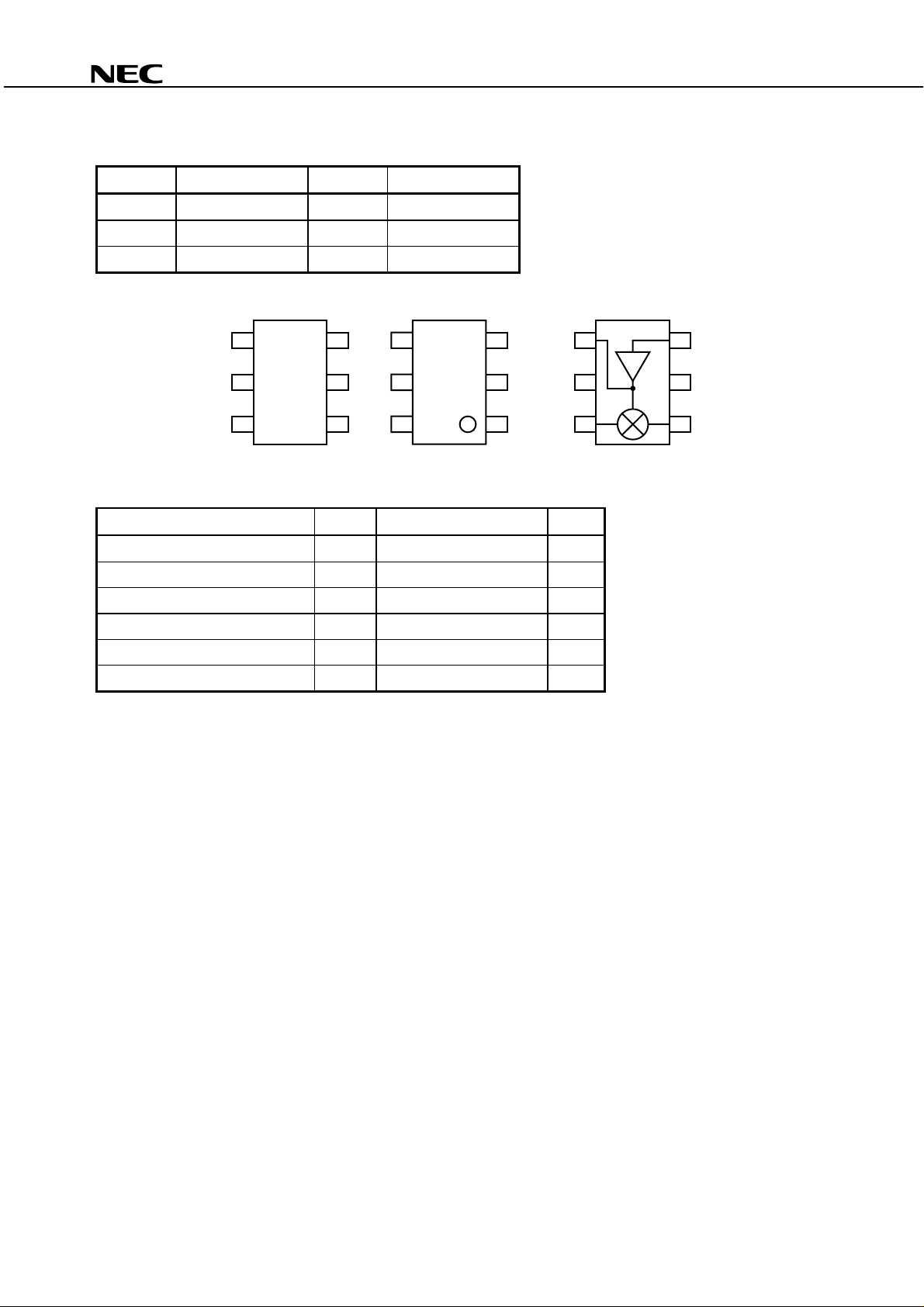
PIN CONNECTIONS
Pin No. Connection Pin No. Connection
1 RF or IF 4 LO IN
2 GND 5 GND
3VDD6IF or RF
Top View Bottom View Top View
µµµµ
PG2121TB
3
2
1
4
5
G2E
6
4
5
6
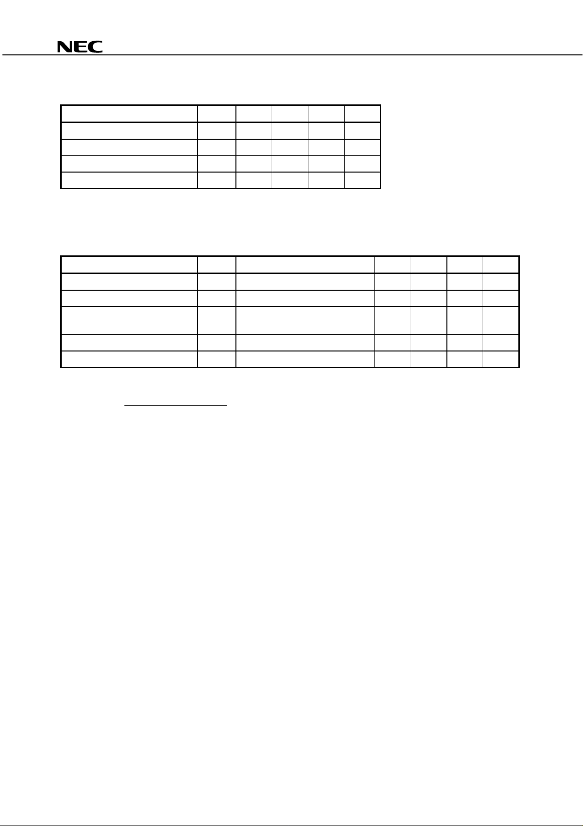
ABSOLUTE MAXIMUM RATINGS (TA = +25
Parameter Symbol Ratings Unit
Supply Voltage V
LO Input Power P
RF Input Power P
Total Power Dissipation P
Operating Ambient Temperature T
Storage Temperature T
Mounted on a 50 × 50 × 1.6 mm double copper clad epoxy glass PWB, T
Note
DD
LO
RF
tot
A
stg
3
2
1
C)
°°°°
6.0 V
+10 dBm
+10 dBm
Note
140
−
30 to +90
−
35 to +150
mW
°
C
°
C
3
2
1
A
= +85 °C
4
5
6
2
Preliminary Data Sheet P15014EJ1V0DS00
µµµµ
PG2121TB
ELECTRICAL CHARACTERISTICS (TA = +25
Parameter Symbol MIN. TYP. MAX. Unit
Supply Voltage V
RF Frequency f
IF Frequency f
LO Input Power P
DD
RF
IF
LO
+2.7 +2.8 +3.0 V
810
50
−
10
ELECTRICAL CHARACTERISTICS
(Unless otherwise specified, T
LO
f
= 940 MHz, PLO =
Parameter Symbol Test Condition MIN. TYP . MAX. Unit
Total Current I
Conversion Loss L
3rd Order Distortion Input Int erc ept
Note
Point
3rd Order Intermoduration Distorti on IM
Local Leackage L
5 dBm, fIF = 90 MHz, f
−−−−
A
= +25
C, VDD = 2.8 V, f
°°°°
IM3
DD
C
3
IIP
3
LO
= 90.1 MHz)
C)
°°°°
−
−
−
50dBm
960 MHz
400 MHz
RF1
= 850 MHz, f
RF2
= 850.1 MHz, P
−
−−
+18 +23
−−52−
−−13−
RF1
RF2
= P
=
3 dBm,
−−−−
3.5 4.5 mA
6.0
−
7.5 dB
−
42 dBc
11 dBm
dBm
3
is determined by comparing two method; theoretical calculation and cross point of IM3 curve.
IIP
Note
IM3 × PRF + CG − P
IIP3 = [dBm]
∆
IM3 − 1
∆
Calculated as ∆IM3 = 3
IM3
IM3: P
∆
IM3
gradient
Preliminary Data Sheet P15014EJ1V0DS00
3
 Loading...