

NEC UPG181GR-E1, UPG181GR Datasheet

DATA SHEET
GaAs INTEGRATED CIRCUIT
µµµµ
PG181GR
GaAs MMIC DBS Twin IF Switch
DESCRIPTION
The µPG181GR is intended for use in Direct Broadcast Satellite (DBS) applications within the Low Noise Block
(LNB) down-converter for systems where at least two LNB outputs are required.
It offers two intermediate frequency amplifier channels that can independently select 1 of 2 IF inputs. It is loused
in a very small 16-pin plastic HTSSOP package available on tape-and-reel and easy to install and contributes to
miniaturizing the systems.
FEATURES
• Two Independent IF Channels
• Integral Switching to Channel Input to Either Channel Output
• Insertion Loss Per Channel : 5.0 dB TYP. (ZO = 50 Ω)
• Frequency Range : 950 MHz to 2 150 MHz
• Channel to Channel Isolation : 33 dB TYP.
• Small 16-pin HTSSOP Package
ORDERING INFORMATION (PLAN)
Part Number Package Supplying Form
µ
PG181GR-E1 16-pin Plastic HTSSOP Carrier tape width 12 mm.
Qty 3 kp/reel.
Remark
Caution The IC must be handled with care to prevent static discharge because its circuit composed of
To order evaluation samples, please contact your local NEC sales office. (Part number for sample
order:
GaAs MES-FET.
PG181GR)
µ
The information in this document is subject to change without notice. Before using this document, please
confirm that this is the latest version.
Not all devices/types available in every country. Please check with local NEC representative for
availability and additional information.
Document No. P14268EJ2V0DS00 (2nd edition)
Date Published November 1999 N CP(K)
Printed in Japan
The mark shows major revised points.
1999©
µµµµ
PG181GR
ABSOLUTE MAXIMUM RATINGS (TA = +25
C)
°°°°
Parameter Symbol Ratings Unit
Note 1
6 to +6
Control Voltage 1, 2, 3, 4 V
CONT1, 2, 3, 4
Total Power Dissipat i on P
Operating Ambient Temperature T
Storage Temperature T
Notes 1.
CONT(H)
| V
Mounted on 50 × 50 × 1.6 mm double copper clad epoxy glass PWB, TC = +85 °C
2.
− V
CONT(L)
| ≤ 6.0 V
tot
A
stg
−
Note2
2
40 to +85
−
65 to +150
−
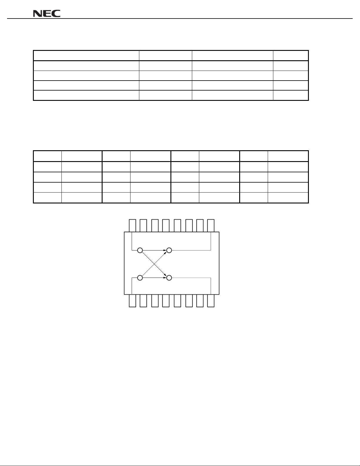
PIN CONNECTION AND INTERNAL BLOCK DIAGRAM (TOP VIEW)
Pin No. Connection P i n No. Connecti on Pin No. Connection P i n No. Connecti on
1IN25V
2 GND 6 GND 10 GND 14 GND
3 GND 7 GND 11 GND 15 GND
4V
CONT3
8OUT212V
CONT4
9OUT113V
CONT2
16 IN1
V
W
°
°
CONT1
C
C
16 15 14 13 12 11 10 9
12345678
2
Data Sheet P14268EJ2V0DS00

µµµµ
PG181GR
RECOMMENDED OPERATING CONDITIONS (TA = +25
C)
°°°°
Parameter Symbol MIN. TYP. MAX. Unit
Control Voltage (High) V
Control Voltage (Low) V
ELECTRICAL CHARACTERISTICS (TA = +25
O
0/ +5 V, Z
= 50
, LL, LR, RL, RR Each Port)
ΩΩΩΩ
CONT(H)
CONT(L)
+4.5 +5 +5.5 V
0.5 0 +0.5 V
−
C, unless otherwise specified: V
°°°°
CONT1
Parameter Sym bol Test Conditions MIN. TYP. MAX. Unit
Insertion Loss L
Insertion Loss Flatness
Insertion Loss Flatness
INS
INS
L
∆
INS
L
∆
f = 0.95 GHz to 2.15 GHz
INS
| L
(0.95 GHz) − L
INS
| L
(0.95 GHz) − L
INS
(1.7 GHz) |
INS
(2.15 GHz) |
−
−
−
5.0 7.0 dB
0.5 1.2 dB
0.8 1.5 dB
Channel Isolation ISL f = 0.95 GHz to 1.7 GHz 30 33
Channel Isolation ISL f = 1.7 GHz to 2.15 GHz 25 30
CONT
out
f = 0.95 GHz to 2.15 GHz 13 16
CONT
V
= +5 V/0 V, RF OFF
−−
Output Return Loss RL
Control Current I
to V
−
−
−
200
CONT4
=
dB
dB
dB
µ
A
Data Sheet P14268EJ2V0DS00
3
EVALUATION CIRCUIT
µµµµ
PG181GR
CONT1
V
to V
IN1
(L)
IN2
(R)
CONT4
= 0/ +5 V, ZO = 50
Z
Z
, DC Blocking Capacitor = 51 pF
ΩΩΩΩ
V
CONT1
V
CONT2
C = 51 pF C = 51 pF
1 000 pF 1 000 pF
O
= 50 Ω ZO = 50 Ω
16
1
O
= 50 Ω ZO = 50 Ω
9
8
1 000 pF 1 000 pF
C = 51 pF C = 51 pF
OUT1
OUT2
CHANNEL SELECT TRUTH TABLE
Output Control Pin
OUT1 OUT2
LL
LR
RL
RR
On Channel
IN1 − OUT1
IN1 − OUT2
IN1 − OUT1
IN2 − OUT2
IN2 − OUT1
IN1 − OUT2
IN2 − OUT1
IN2 − OUT2
V
CONT3
V
CONT4
V
CONT1
V
CONT2
V
CONT3
V
CONT4
Low High High Low
Low High Low High
High Low High Low
High Low Low High
4
Data Sheet P14268EJ2V0DS00
 Loading...