

©
1996
DATA SHEET
GaAs INTEGRATED CIRCUIT
µµ
µµ
µ
PG103B
µ
PG103B is GaAs integrated circuit designed as wide band (50 MHz to 3GHz) amplifiers.
This device is most suitable for the microwave communication system and the measurement equipment.
FEATURES
• Ultra wide band : f = 50 MHz to 3 GHz
• Input/output impedance matched to 50 Ω
• Hermetic sealed ceramic package assures high reliability
ORDERING INFORMATION
PART NUMBER PACKAGE
µ
PG103B T-31, 8 PIN CERAMIC
ABSOLUTE MAXIMUM RATINGS (TA = 25 ˚C)
Drain Voltage VDD +8 V
Gate Voltage VGG –8 V
Input Voltage V
in –3 to +0.6 V
Input Power Pin +15 dBm
Total Power Dissipation* Ptot 1.5 W
Operating Case Temperature T
opt –65 to +125 ˚C
Storage Temperature Tstg –65 to +175 ˚C
* TC ≤ 125 ˚C
RECOMMENDED OPERATING CONDITIONS (TA = 25 ˚C)
Drain Voltage VDD +5.0±0.5 V
Gate Voltage V
GG –5.0±0.5 V
Operating Case Temperature Topt –50 to +80 ˚C
Document No. P11342EJ1V0DS00 (1st edition)
Date Published March 1996 P
Printed in Japan
WIDE-BAND AMPLIFIER
µµ
µµ
µ
PG103B
2
ELECTRICAL CHARACTERISTICS (TA = 25 ˚C, VDD = +5V, VGG = –5V)
CHARACTERISTIC SYMBOL MIN. TYP. MAX. UNIT TEST CONDITIONS
Drain Current IDD 40 55 80 mA RF OFF
Gate Current IGG 12mA
Power Gain Gp 12 dB f = 0.05 to 2 GHz
Power Gain Gp 10 dB f = 2 to 3 GHz
Gain Flatness Gp ±1.5 ±2.0 dB f = 0.05 to 2 GHz
Gain Flatness Gp ±2.0 ±3.0 dB f = 0.05 to 3 GHz
Noise Figure NF 4.0 4.5 dB f = 0.05 to 2 GHz
Noise Figure NF 4.5 5.0 d B f = 2 t o 3 G Hz
Input Return Loss RLin 6 10 dB f = 0.05 to 1 GHz
Input Return Loss RLin 10 14 dB f = 1 to 2 GHz
Input Return Loss RLin 6 10 dB f = 2 to 3 GHz
Output Return Loss RLout 10 16 dB
Isolation ISOL 30 40 dB f = 0.05 to 3 GHz
Output Power at 1 dB Gain
Compression Point
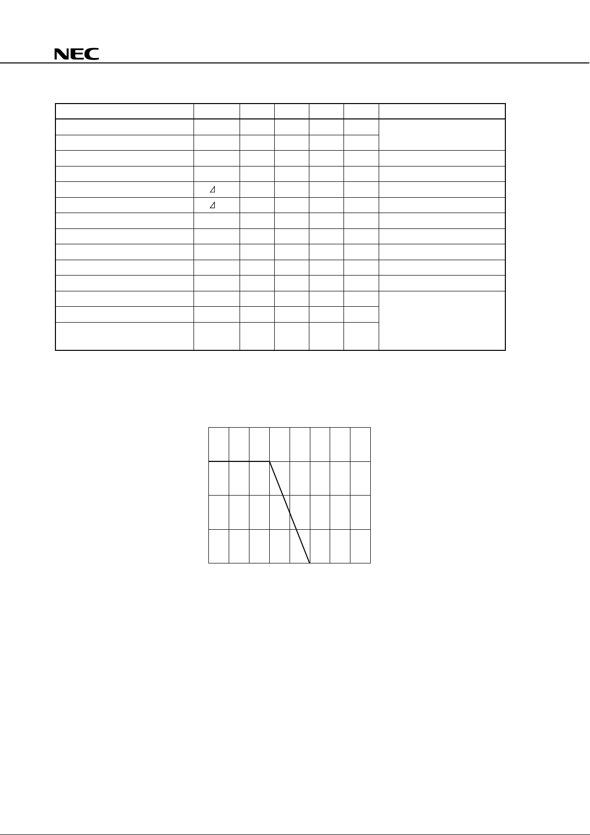
TYPICAL PERFORMANCE CURVES
Po (1dB) +7 +9 dBm
D.C. POWER DERATING CURVE
2.0
1.5
1.0
0.5
0 50 100 125 150 200
T
C
- Case Temperature - °C
P
T
- Total Power Dissipation - W
µµ
µµ
µ
PG103B
3
OUTPUT POWER vs. INPUT POWER
VDD = +5 V
V
GG = –5 V
f = 1 GHz
2 GHz
3 GHz
P
i - Input Power - dBm
–10 0–20
+10
+5
0
ISOLATION vs. FREQUENCY
V
DD = +5 V
VGG = –5 V
f - Frequency - MHz
10
10
20
30
40
50
Po - Output Power - dBm
I
SOL - Isolation - dB
20 50 100 500 1000 5000
INPUT AND OUTPUT RETURN LOSS vs.
FREQUENCY
V
DD = +5 V
VGG = –5 V
f - Frequency - MHz
10
0
10
20
30
40
RL - Return Loss - dB
20 50 100 500 1000 5000200
200
in
out
POWER GAIN AND NOISE FIGURE vs.
FREQUENCY
V
DD = +5 V
VGG = –5 V
f - Frequency - MHz
10
20
Gp - Power Gain - dB
20 50 100 500 1000 5000200
10
0
10
5
NF - Noise Figure - dB
GP
NF

µµ
µµ
µ
PG103B
4
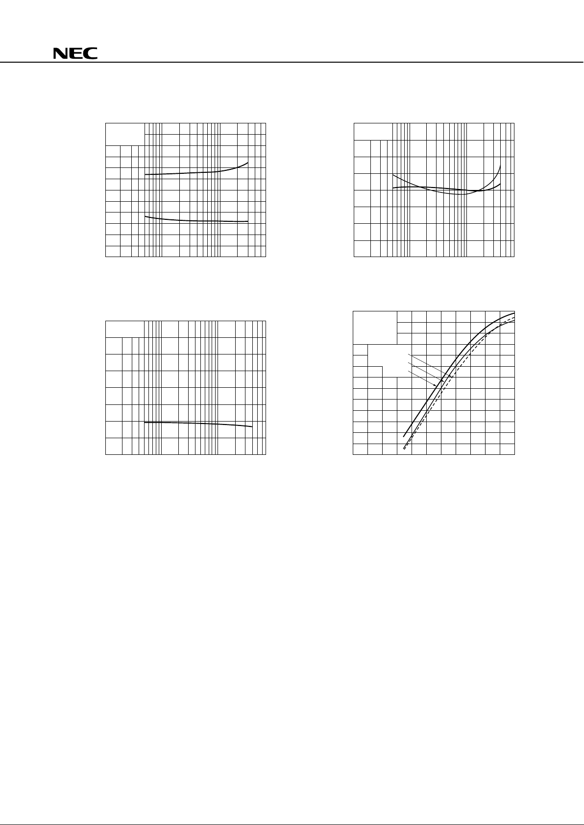
TEST CIRCUIT
EQUIVALENT CIRCUIT
V
DD
1000 pF
IN 100 pF*
7
3
15
100 pF* OUT
2, 4, 6, 8
V
GG
1000 pF
* Chip capacitor
V
DD
C1 L3 C2
RL1
RL2
RL2
L2 C4C3
RF1
R1 R2
R3
R4
R5
R6
OUT
L1
IN
V
GG

µµ
µµ
µ
PG103B
5
OUTLINE DIMENSIONS (Unit : mm)
1.27±0.11.27±0.1
4–0.6 4–0.4
432
15
678
3.8±0.2
10.6 MAX.
10.6 MAX.
1.7 MAX.
0.2
+0.05
–0.02
PACKAGE OUTLINE
PIN CONNECTIONS:
1. INPUT
2. GND
3. V
GG
4. GND
5. OUTPUT
6. GND
7. V
DD
8. GND

µµ
µµ
µ
PG103B
6
RECOMMENDED SOLDERING CONDITIONS
The following conditions (see table below) must be met when soldering this product.
Please consult with our sales offices in case other soldering process is used, or in case soldering is done under
different conditions.
TYPES OF SURFACE MOUNT DEVICE
For more details, refer to our document “SEMICONDUCTOR DEVICE MOUNTING TECHNOLOGY MANUAL”
(C10535EJ7V0IF00).
µ
PG103B
Soldering process Soldering conditions Symbol
Infrared ray reflow Peak package’s surface temperature: 230 ˚C or below,
Reflow time: 10 seconds or below (210 ˚C or higher),
Number of reflow process: 1, Exposure limit*: None
Partial heating method Terminal temperature: 260 ˚C or below,
Flow time: 10 seconds or below,
Exposure limit*: None
* Exposure limit before soldering after dry-pack package is opened.
Storage conditions: 25 ˚C and relative humidity at 65 % or less.
Note Do not apply more than a single process at once, except for “Partial heating method”.
PRECAUTION This IC must be handled with great care to prevent static discharge because its circuitry is
composed of GaAs MES FET.
Caution
The Grate Care must be taken in dealing with the devices in this guide.
The reason is that the material of the devices is GaAs (Gallium Arsenide), which is
designated as harmful substance according to the Japanese law concerned.
Keep the Japanese law concerned and so on, especially in case of removal.

µµ
µµ
µ
PG103B
7
[MEMO]

2
µµ
µµ
µ
PD103B
No part of this document may be copied or reproduced in any form or by any means without the prior written
consent of NEC Corporation. NEC Corporation assumes no responsibility for any errors which may appear in this
document.
NEC Corporation does not assume any liability for infringement of patents, copyrights or other intellectual
property rights of third parties by or arising from use of a device described herein or any other liability arising
from use of such device. No license, either express, implied or otherwise, is granted under any patents,
copyrights or other intellectual property rights of NEC Corporation or others.
While NEC Corporation has been making continuous effort to enhance the reliability of its semiconductor devices,
the possibility of defects cannot be eliminated entirely. To minimize risks of damage or injury to persons or
property arising from a defect in an NEC semiconductor device, customer must incorporate sufficient safety
measures in its design, such as redundancy, fire-containment, and anti-failure features.
NEC devices are classified into the following three quality grades:
“Standard“, “Special“, and “Specific“. The Specific quality grade applies only to devices developed based on
a customer designated “quality assurance program“ for a specific application. The recommended applications
of a device depend on its quality grade, as indicated below. Customers must check the quality grade of each
device before using it in a particular application.
Standard: Computers, office equipment, communications equipment, test and measurement equipment,
audio and visual equipment, home electronic appliances, machine tools, personal electronic
equipment and industrial robots
Special: Transportation equipment (automobiles, trains, ships, etc.), traffic control systems, anti-disaster
systems, anti-crime systems, safety equipment and medical equipment (not specifically designed
for life support)
Specific: Aircrafts, aerospace equipment, submersible repeaters, nuclear reactor control systems, life
support systems or medical equipment for life support, etc.
The quality grade of NEC devices in “Standard“ unless otherwise specified in NEC's Data Sheets or Data Books.
If customers intend to use NEC devices for applications other than those specified for Standard quality grade,
they should contact NEC Sales Representative in advance.
Anti-radioactive design is not implemented in this product.
M4 94.11
 Loading...