

DATA SHEET
MOS INTEGRATED CIRCUIT
µ
PD9930
LINEAR CODEC FOR DIGITAL CELLULAR TELEPHONE
The µPD9930 is a +3 V single power operation, low power consumption linear CODEC LSI developed for digital
cellular telephone use.
CODEC has a wide dynamic use.
This IC also features a microphone/receiver amplifier, a tone generator, DAI (Digital Audio Interface: conforming
to GSM11.10), and a power-saving function. These functions can be controlled by microcontroller.
In addition, 21 mW (TYP.) low power consumption is enabled during 3 V operation.
FEATURES
• +3 V single power supply
• Low power consumption
In operation: 7 mA (TYP.) (VDD = 3 V)
In stand-by mode: 50 µA (TYP.) (VDD = 3 V)
• CODEC
• 13-bit precision linear coding
• Transmission level can be controlled by microcontroller.
• Analog input/output funciton
• Low noise microphone amplifier
• High output receiver amplifier
Piezo-electric receiver can be directly driven.
Gain canbe controlled by microcontroller.
• On-chip amplifier for accessory input/output
• Tone generator
• Frequency, generating pattern and gain can be controlled
by microcontroller.
• DTMF generation function
• Various service tone generation function
• GSM triple tone generation function
• Desired tone frequency can be registered (0.3 to 3.4 kHz)
ORDERING INFORMATION
Part Number Package
µ
PD9930G-22 44-pin plastic QFP (10 × 10 mm)
• DAI
• Conforming to GSM11.10
• Test mode can be set by terminal or microcontroller
command.
• Stand-by mode
• Rise time at time of stand-by clearing: 30.5 ms (TYP.)
• Master clock generation PLL (external clock input: 8 kHz)
• Tone interrupt pattern output function
• Ringer output function
The information in this document is subject to change without notice.
Document No. S11616EJ2V0DS00 (2nd edition)
(Previous No. IC-3342)
Date Published November 1996 N
Printed in Japan
The mark shows major revised points.
©
1994,1996
2
BLOCK DIAGRAM
RESETB
(15 to 33 dB)
(to XACOMO)
(0 to 10 dB)
REC2O–
REC2O+
XACOMI
XACOMO
RACOMO
MIXI
MICO
MICI–
MICI+
XAUXO
XAUXI–
RAUXO
REC1O
REC2I–
Microphone
amplifier
–
+
Accessory input
amplifier
to V
–
+
ref
Post Filter 1
(Accessory output
amplifier)
0 dB fix
Post Filter 2
(Receiver amplifier 1)
0 to -31 dB
(1 dB steps)
Receiver drive amplifier
(Receiver amplifier 2)
V
combuff
Digital signal processor
PLL
Voice send
Pre-Filter
+ Mixer
0 or –3 dB
A/D
Digital
Gain Cont.
0 to –2.8 dB
(0.4 dB steps)
Transmit
BPF
DSP
INTERFACE
Voice receive
D/A
Receive
LPF
Digital
Gain Cont.
0 to –2.4 dB
(0.8 dB steps)
MICRO-
CONTROLLER
INTERFACE
–
+
to V
ref
Sign code
output
Tone
Gain Cont.
0 to –30 dB
(1 dB steps)
–38.5 dB
Tone
Generator
–
+
to V
ref
DAI
Tone Interval
(GSM11. 10)
Generation
V
ref
REQB
FSYNC
(8 kHz)
SCLK
(256 kHz)
SEN
SO
SI
DSPSEL
MCLK
MSTR
MDAT
DCLK
DO
DI
TC1
TC2
DRSTB
RACOMI
RINGER
Low-current drive LED
TIMER
µ
PD9930
PIN CONFIGURATION (Top View)
44-pin plastic QFP (10 x 10 mm)
Note
REC2I–
IC
33 32 31 30 29 28 27 26 25 24 23
REC1O
34
REC2O–
REC2O+
RACOMI
RACOMO
XACOMO
XACOMI
XAUXI–
XAUXO
MIXI
22
µ
PD9930
MICO
RAUXO
DD1
AV
AV
DD2
DV
SEN
SO
SCLK
TEST
MSTR
35
36
37
DD
SI
38
39
40
41
42
43
44
1234567891011
DI
MDAT
MCLK
DO
DRSTB
DCLK
TC1
TC2
TIMER
RINGER
DSPSEL
21
20
19
18
17
16
15
14
13
12
MICI–
MICI+
AGND4
AGND3
AGND2
AGND1
DGND
FSYNC
RESETB
REQB
Note Internal connection; leave unconnected
3

Pin Name
AGND1-AGND4 : Analog Ground
AVDD1, AVDD2 : Analog Power Supply
DCLK : DAI (Digital Audio Interface) Clock Output
DGND : Digital Ground
DI : DAI Serial Input
DO : DAI Serial Output
DRSTB : DAI Reset
DSPSEL : Digital Signal Processor Select
DD : Digital Power Supply
DV
FSYNC : Frame Synchronization Signal Input
IC : Internally Connected
MCLK : Microcontroller Synchronous Clock
MDAT : Microcontroller Serial Data
MICI+ : Microphone Amplifier Input Non-Inverted
MICI– : Microphone Amplifier Input Inverted
MICO : Microphone Amplifier Output
MIXI : Mixer Input
MSTR : Microcontroller Strobe
RACOMI : Receive Common Reference Voltage Input
RACOMO : Receive Common Reference Voltage Output
RAUXO : Receive Auxiliary Amplifier Output
REC1O : Receive Amplifier 1 Output
REC2I– : Receive Amplifier 2 Input Inverted
REC2O+ : Receive Amplifier 2 Output Non-Inverted
REC2O– : Receive Amplifier 2 Output Inverted
REQB : Request
RESETB : Reset
RINGER : Ringer
SCLK : Serial Data Synchronous Clock Output
SEN : Serial Data Output Enable
SI : Serial Data Input
SO : Serial Data Output
TC1, TC2 : DAI Mode Control
TEST : Test
TIMER : Timer
XACOMI : Transmit Common Reference Voltage Input
XACOMO : Transmit Common Reference Voltage Output
XAUXI– : Transmit Auxiliary Amplifier Input Inverted
XAUXO : Transmit Auxiliary Amplifier Output
µ
PD9930
4

µ
PD9930
CONTENTS
1. PIN FUNCTIONS ...........................................................................................................................6
1.1 LIST OF PIN FUNCTIONS ..................................................................................................................... 6
1.2 PIN EQUIVALENT CIRCUIT .................................................................................................................. 8
2. BLOCK FUNCTIONS .....................................................................................................................9
2.1 CODEC .................................................................................................................................................... 9
2.1.1 Audio Codec..............................................................................................................................9
2.1.2 Audio Analog Input .................................................................................................................. 9
2.1.3 Audio Analog Output ............................................................................................................. 10
2.1.4 Audio Digital Accessory Output ........................................................................................... 11
2.1.5 Audio Digital Signal Processor ............................................................................................ 11
2.1.6 Power Up/Down Control ........................................................................................................ 12
2.1.7 Microcontroller Interface ....................................................................................................... 18
2.1.8 DSP Interface .......................................................................................................................... 19
2.1.9 DAI (Digital Audio Interface) ................................................................................................. 22
3. TONE INTERVAL OUTPUT FUNCTION (TIMER TERMINAL)................................................. 29
4. INTERNAL CONTROL FUNCTIONS ...........................................................................................30
4.1 SEND/RECEIVE GAIN CONTROL ...................................................................................................... 30
4.1.1 Voice Send Analog Gain/Receiver Amplifier 2 Control Register (TXGCR) .................... 32
4.1.2 Voice Receive Analog Gain Control Register (RXGCR) ................................................... 3 3
4.1.3 Voice Send/Receive Digital Gain Control Register (DGGSR) .......................................... 35
4.2 DIGITAL INPUT/OUTPUT CONTROL ................................................................................................. 37
4.2.1 Digital Signal Processing Control Register (DSPCR) ....................................................... 38
4.3 TONE CONTROL..................................................................................................................................40
4.3.1 Tone Frequency Selection Register (FRQSR)....................................................................43
4.3.2 Expanded Tone Registers (EXPR1, EXPR2) ....................................................................... 45
4.3.3 Tone Control Register (TONCR)...........................................................................................47
4.3.4 Tone Gain Control Register (TNGCR) ................................................................................. 48
4.4 TEST MODE CONTROL ...................................................................................................................... 50
4.4.1 Test Control Register (TSTCR).............................................................................................52
5. ELECTRICAL CHARACTERISTICS ............................................................................................53
6. APPLIED CIRCUIT EXAMPLE ....................................................................................................73
7. PACKAGE DRAWINGS ...............................................................................................................74
8. RECOMMENDED SOLDERING CONDITIONS ......................................................................... 7 5
5
1. PIN FUNCTIONS
1.1 LIST OF PIN FUNCTIONS
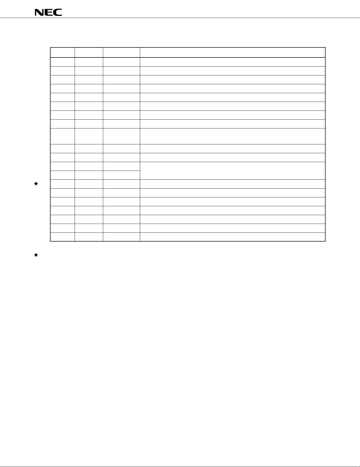
Table 1-1 List of Pin Functions (1/2)
Pin No. Pin Name Input/Output Function
1 MDAT Input Microcontroller interface serial input
2 MCLK Input Microcontroller interface clock input
3 DRSTB Input DAI (Digital Audio Interface) reset input
This is reset at low level. Internally pulled high.
4 DI Input DAI serial input
Internally pulled high.
5 DO Output DAI serial output
Hi-Z in normal operation (TC1 = TC2 = low level)
6 DCLK Output DAI clock output (104 kHz)
Hi-Z in normal operation
7 TC1 Input
8 TC2 Input
DAI mode control
Selection of test mode specified by
GSM11.10 in combination with TC1
and TC2
L: Low level
H: High level
TC2 TC1 Test mode specification
L L Normal operation
L H Speech encoder test mode
H L Speech decoder test mode
H H Acoustic device test mode
µ
PD9930
TC1 and TC2 pins are internally pulled down.
9 TIMER Output Timer output. Output of rectangular wave synchronized with tone intermittent
pattern.
10 RINGER Output Ringer tone output. Output of rectangular wave synchronized with tone fre-
quency.
11 DSPSEL Input Selection of DSP interface input/output timing mode.
Connect to VDD or GND. (VDD = mode 1, GND = mode 2)
12 REQB Input Input of DSP interface data transmit request signal.
Serial data can be input/output at low level.
13 RESETB Input System reset input. This is reset at low level. Initializes all control registers.
Reset when turning power on.
14 FSYNC Input Send/receive frame synchronization signal (8 kHz) input
15 DGND — Digital ground. Connect to a digital ground line near µPD9930 pins.
16 AGND1 — Analog ground. Connect to an analog ground line near µPD9930 pins.
17 AGND2 —
18 AGND3 —
19 AGND4 —
20 MICI+ Input Microphone amplifier non-inverted input
21 MICI– Input Microphone amplifier inverted input
22 MICO Output Microphone amplifier output. Connect microphone amplifier gain adjust resistor.
Outputs sidetone signal to REC2I- pin.
23 MIXI Input Pre-filter + mixer input
24 XAUXO Output Accessory input amplifier output. Connect accessory input amplifier gain adjust
resistor.
6
µ
Table 1-1 List of Pin Functions (2/2)
Pin No. Pin Name Input/Output Function
25 XAUXI– Input Accessory input amplifier inverted input
26 XACOMI Input Voice send internal reference voltage input
27 XACOMO Output Voice send internal reference voltage (1.2 V) output
28 RACOMO Output Voice receive internal reference voltage (1.2 V) output
29 RACOMI Input Voice receive internal reference voltage input
30 REC2O+ Output Receiver amplifier 2 non-inverted output
31 REC2O– Output Receiver amplifier 2 inverted output
32 IC — Internal connection; leave unconnected
33 REC2I– Input Receiver amplifier 2 inverted input
Connect sidetone gain adjust resistor.
34 REC1O Output Receiver amplifier 1 output
35 RAUXO Output Accessory output amplifier output
36 AVDD1 — Analog power. Connect to an analog power supply line near µPD9930 pins.
37 AVDD2 —
38 DVDD — Digital power. Connect to a digital power supply line near µPD9930 pins.
39 SEN Output DSP interface enable signal output
40 SI Input DSP interface serial input
41 SO Output DSP interface serial output
42 SCLK Output DSP interface clock output (256 kHz)
43 TEST Input Set at high level
44 MSTR Input Microcontroller interface strobe signal input
PD9930
Caution Short-circuit the XACOMI and XACOMO pins at a location as close to the pins of the µPD9930 as
possible. Connect a capacitor (chip capacitor or electrolytic capacitor) between this short-circuited
portion and analog ground.
The same applies to the RACOMI and RACOMO pins.
The transmission/reception level is determined by these reference pins. Therefore, make sure that
these pins are not affected by noise or fluctuation of ground potential due to current.
7
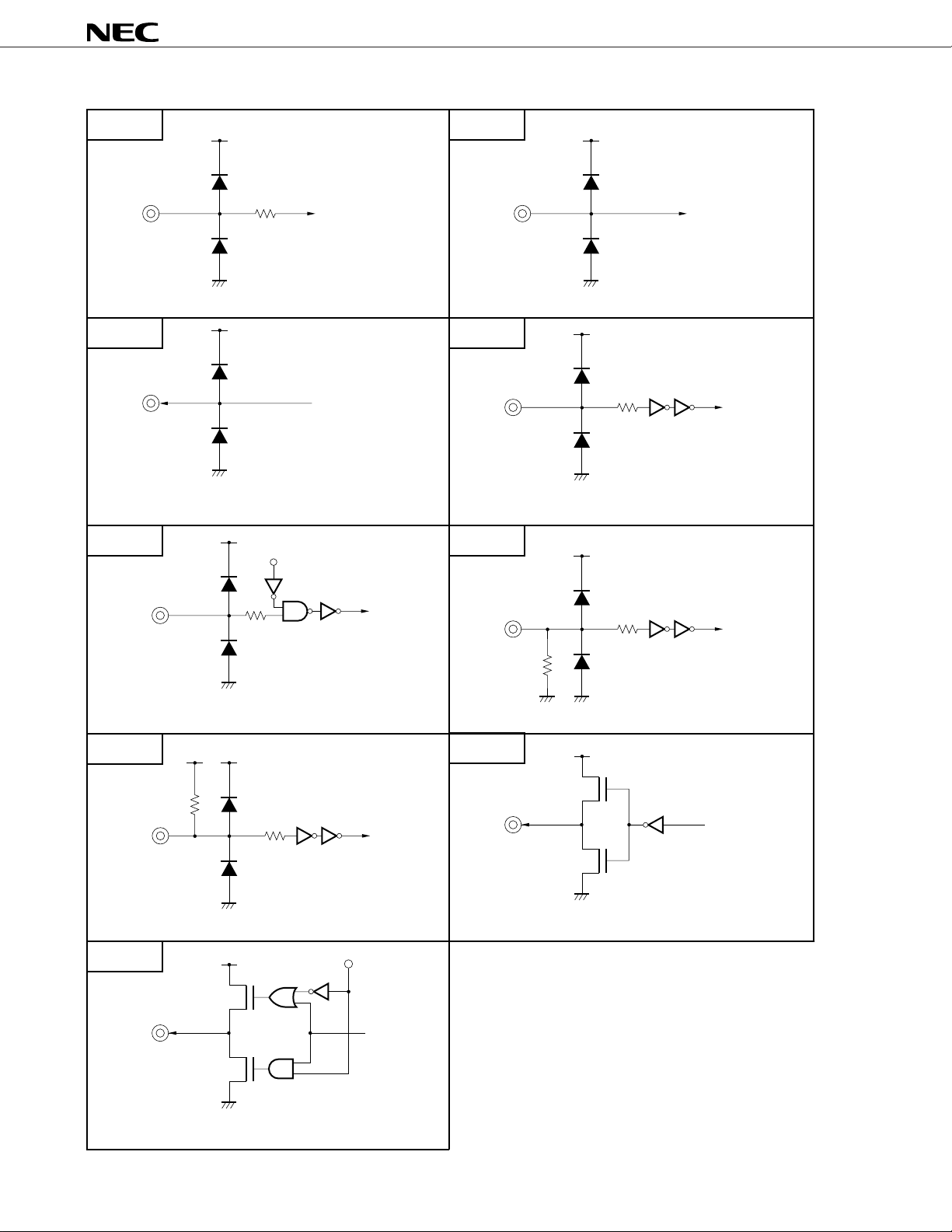
1.2 PIN EQUIVALENT CIRCUIT
AV
DD
µ
PD9930
Type 2Type 1
AV
DD
Analog input
To internal circuit
AGND
Pin Name MICI+, MICI–, XAUXI–, REC2I–
AV
Type 3
DD
Analog output
From internal circuit
AGND
Pin Name MICO, XAUXO, XACOMO, RACOMO,
REC2O+, REC2O–, REC1O, RAUXO
DV
Type 5
DD
Mask input
CMOS input
To internal
circuit
Analog input
AGND
Pin Name MIXI, XACOMI, RACOMI
DV
Type 4
DD
CMOS input
DGND
Pin Name MDAT, MCLK, DSPSEL, REQB,
RESETB, FSYNC, TEST, MSTR
Note
Type 6
DV
DD
CMOS input
To internal circuit
To internal
circuit
To internal
circuit
Pin Name SI
Note
Type 7
DV
DD
CMOS input
Pin Name DRSTB, DI
Type 9
CMOS output
Pin Name DO, DCLK
DV
DD
P
N
DGND
DGND
DD
DV
DGND
To internal
circuit
Enable signal
From internal
circuit
DGND
Pin Name TC1, TC2
Type 8
DV
DD
P
CMOS output
N
DGND
Pin Name TIMER, RINGER, SEN, SO, SCLK
From internal
circuit
Note In normal mode, set the output of drive IC side to high impedance for reducing power consumption.
8
2. BLOCK FUNCTIONS
2.1 CODEC
2.1.1 Audio Codec
Audio analog signal and linear code conversion.
• Input/output format: 16 bits (2's complement)
• Accuracy: 13 bits
2.1.2 Audio Analog Input
Includes microphone input and accessory input.
(1) Microphone amplifier
Amplifiers differential input signals from the microphone to the required gain.
(2) Accessory input amplifier
Amplifiers the accessory input signal to the required gain.
µ
PD9930
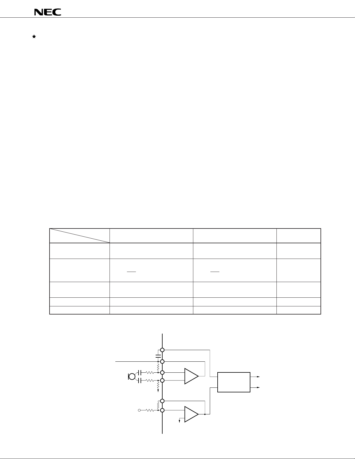
(3) Pre-filter + mixer
Selects the output signal of microphone amplifier and accessory input amplifier, and inputs these to A/D converter
after controlled gain.
Table 2-1 Analog Input Function
Amplifier
Function
Gain setting method External resistor External resistor Microcontroller
Gain setting range 15 to 33 dB 0 to 10 dB 0 or –3 dB
20 log (dB) 20 log (dB)
Minimum resistive load 50 kΩ 300 kΩ —
(Including gain setting resistance) (Including gain setting resistance)
Maximum capacitive load 20 pF 20 pF —
Maximum output level 0.6 V0-p 0.6 V0-p —
Microphone Amplifier Accessory Input Amplifier Pre-filter + Mixer
command
R2 R3
R1 R4
Figure 2-1 Analog Input Block
MIXI
(15 to 33 dB)
(to XACOMO)
(0 to 10 dB)
R1
R1
R4
R2
R3
MICO
MICI–
MICI+
XAUXO
XAUXI–
to V
Microphone
amplifier
–
+
–
+
Accessory input amplifier
ref
Pre-filter +
mixer
0 or –3 dB
9
µ
PD9930
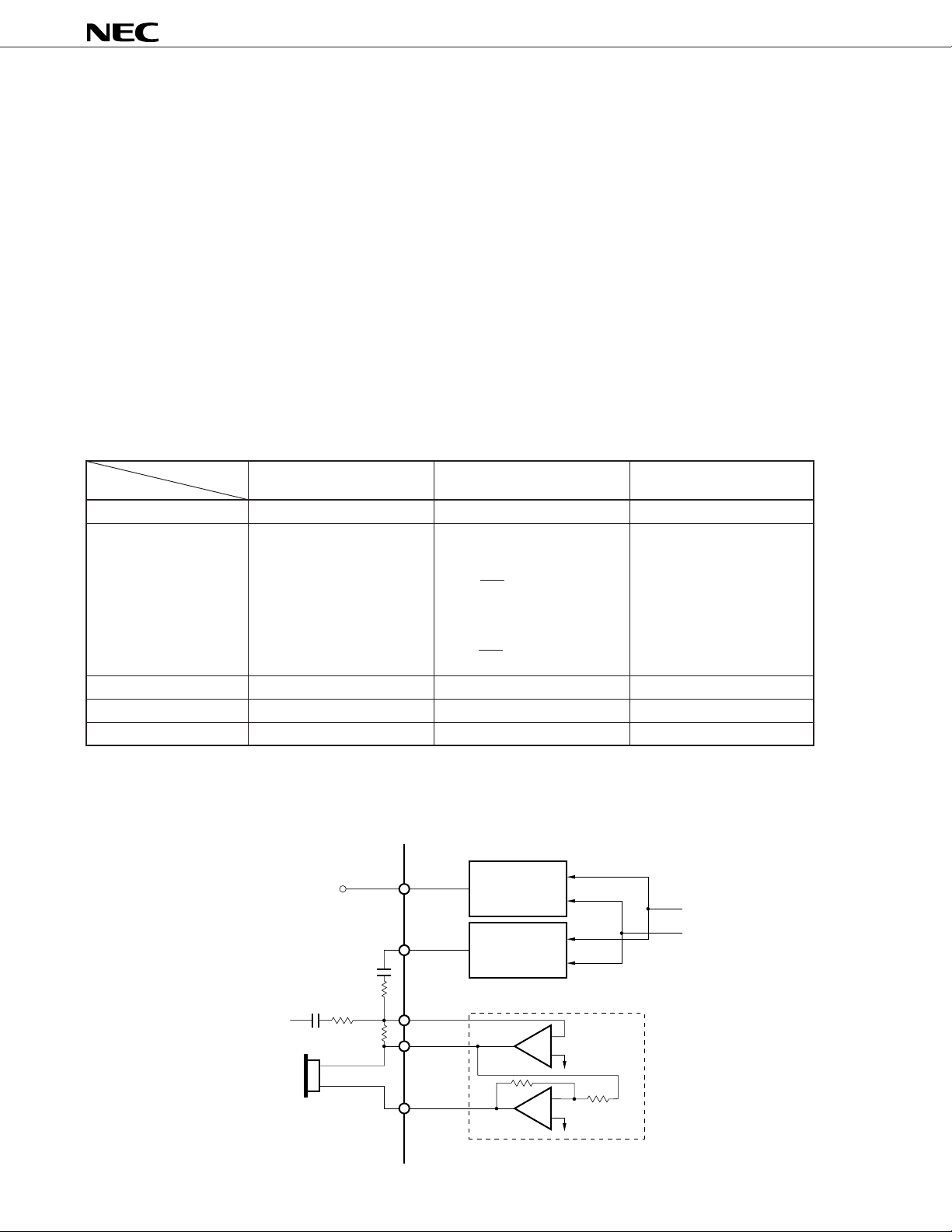
2.1.3 Audio Analog Output
Includes receiver output and accessory output. Sidetone addition is also possible.
(1) Post filter 2 (receiver amplifier 1)
This circuit adjusts the gain of D/A differential output signal (volume control), and then converts it to single output
signal.
(2) Receiver drive amplifier (receiver amplifier 2)
This is differential output amplifier that can directly drive a piezo-electric receiver (when using a dynamic receiver,
an additional external amplifier is necessary). The sidetone is added in this circuit.
(3) Post filter 1 (accessory output amplifier)
This circuit converts D/A differential output signal to single output signal. Connected to the earphone of the head
set (capacitance load), etc.
Table 2-2 Analog Output Functions
Amplifier
Function
Gain setting method Microcontroller command External resistor —
Gain setting range 0 to –31 dB (1 dB steps) Voice receive signal gain: —
Minimum resistive load 100 kΩ 2 kΩ 100 kΩ
Maximum capacitive load 20 pF 60 nF 100 pF
Maximum output level 0.6 V0-p 4 Vp-p (Differential output) 0.6 V0-p
Receiver Amplifier 1 Receiver Amplifier 2 Accessory Output Amplifier
– ∞ to + 10 dB
R3
20 log (dB) + 6 dB
R2
Sidetone signal gain:
– ∞ to + 3 dB
R3
20 log (dB) + 6 dB
R1
Note
Note
Note Conversion result (single output → differential output)
Figure 2-2 Analog Output Block
Post filter 1
(accessory output
amplifier)
0 dB fix
Post filter 2
(receive amplifier 1)
0 to –31 dB
(1 dB steps)
Receiver drive amplifier
(receiver amplifier 2)
–
+
to V
ref
Sidetone signal
R1
R2
R3
RAUXO
REC1O
REC2I–
REC2O–
10
REC2O+
–
+
to V
ref
µ
PD9930
2.1.4 Audio Digital Accessory Output
(1) Ringer output (RINGER pin)
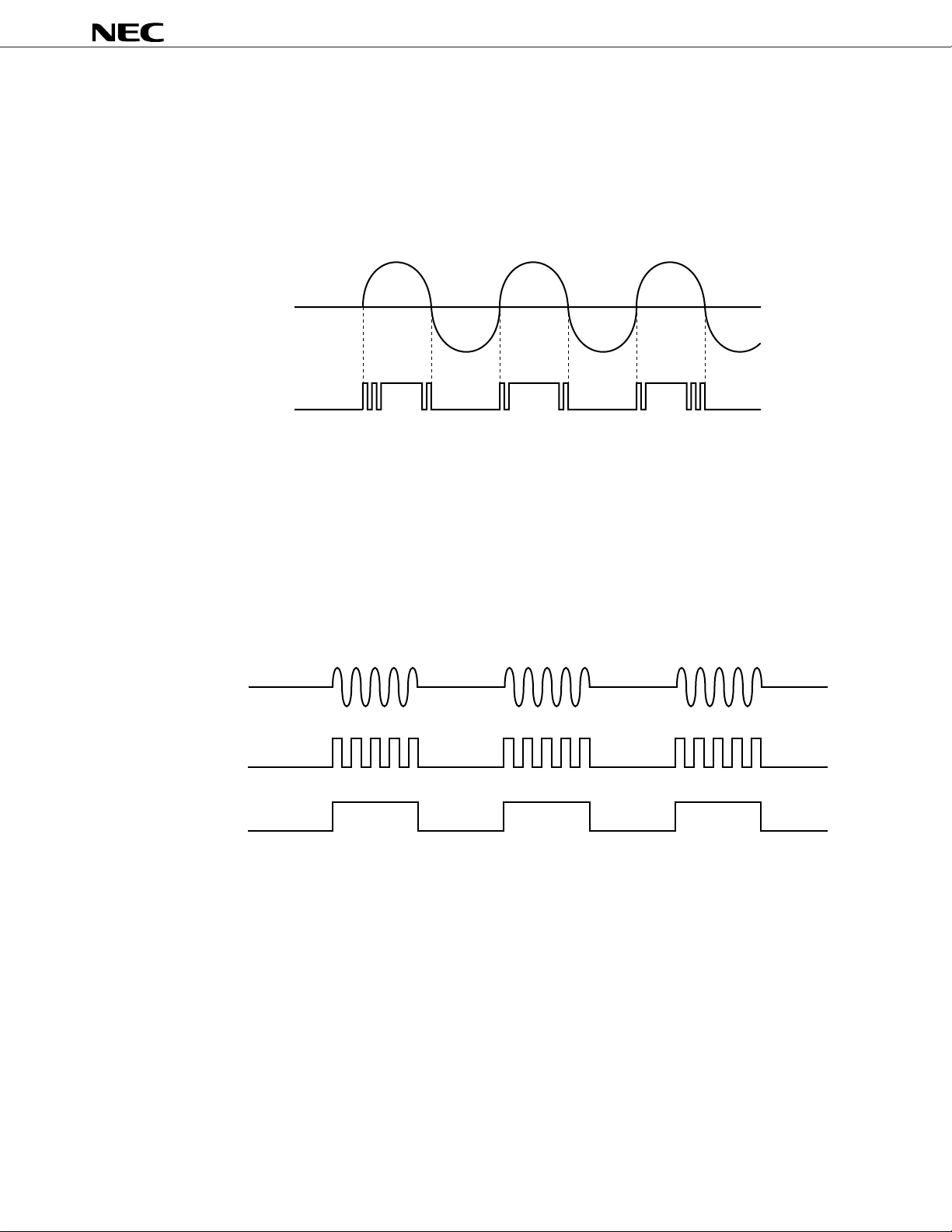
• Outputs rectangular waves of the same signal frequency as tone signal frequency.
• The output is controlled by turning off power to the output buffer with a control register.
Figure 2-3 RINGER Output
RAUXO
(Tone output)
RINGER
The RINGER signal tends to bounce when the tone output (RAUXO) signal crosses its zero level, and this
tendency increases as the tone output gain decreases (lower than 0 dB).
When using RINGER pin, tune the tone output gain by TNGCR (Tone gain control register) to 0 dB.
(2) Timer (tone interval) output (TIMER pin)
Outputs rectangular waves of the same pattern as the tone signal interrupt pattern. This is used to make the
LED blink in synchronization with the ringer tone.
Figure 2-4 Digital Accessory Output Waveform
REC10
RAUXO
(Tone output)
RINGER
TIMER
2.1.5 Audio Digital Signal Processor
Send signal digital BPF processing, receive signal digital LPF processing, transmission level (digital gain)
control, and tone generation processing.
(1) Voice send signal digital gain fine adjustment function
Performs gain fine adjustment for voice send signal by digital coefficient multiplication. Together with prefilter
gain adjustment, fine adjustment is possible at a width of 5.8 dB.
(2) Voice receive signal digital gain fine adjustment function
Performs fine adjustment of gain for voice receive signal by digital coefficient multiplication.
(3) Tone generation function
Generates single-tone and dual-tone audible signals. Tone frequency, interrupt pattern, gain, generation/stop
can be controlled by microcontroller command. GSM triple tone can be generated by special command.
11
Table 2-3 Digital Gain Control Functions
µ
PD9930
Voice Send Signal Gain Control
Gain setting method Microcontroller command Microcontroller command Microcontroller command
Gain setting range 0 to –2.8 dB (0.4 dB steps) 0 to –2.4 dB (0.8 dB steps) 0 to –30 dB (1 dB steps), –38.5 dB
2.1.6 Power Up/Down Control
The µPD9930 includes a power down function for reducing power consumption. Power down control is by
the two methods described below.
(1) Input/output amplifier power up/down control
Power up/down for both the input and output amplifiers can be controlled.
When the power down function is used for all input amplifiers, both pre-filter and A/D enter the power down state.
When the power down function is used for the accessory output amplifier and the receiver 1 amplifier, the D/A
also enters power down state.
(2) Stand-by mode
Low power consumption can be realized in the mode in which all chip operation is stopped. The stand-by mode
is set by power down command. Operation restarts by power up command.
The following control registers are used to enable the control described above.
Control Method Registers Used
Power up/down control of input/output amplifier Input/output amplifier control register (AMPCR)
(not including receiver amplifier 2)
Power up/down control of receiver amplifier 2 Send analog gain/receiver amplifier 2 control register (TXGCR)
Set/clear of standby mode Power up control command (PUPCMD)
Voice Receive Signal Gain Control
Power down control command (PDWCMD)
Tone Gain Control
An outline diagram of power down control is shown in Figure 2-5.
12
Figure 2-5 Power Down Control
µ
PD9930
Register address
0 0 0 MICPDB
XAUXPDB REC1PDB RAUXPDB RINGPDB
Register address
000110
AMPCR
TXGCR
REC2PDB
TXAG
Power up command
011110——
Power down command
011100——
Note M: HEX value with MSB first L: HEX value with LSB first
Stand-by
Pre-filter
+ mixer
When all input amplifiers are
in the power down state,
these also enter power
down state.
A/D
to XACOMI
Microphone input
–
+
"1" = Power ON
Accessory input
–
+
"1" = Power ON
ref
to V
MICPDB
XAUXPDB
ML
78H 1EH
ML
70H 0EH
PLL
Stand-by
Digital signal
processor
HEX
HEX
Note
Note
Accessory output
–
+
"1" = Power ON
Receiver 1
–
+
"1" = Power ON
Receiver 2
Ringer output
–
+
–
+
"1" = Ringer output
to V
to V
RAUXPDB
REC1PDB
ref
ref
RINGPDB
Stand-by
D/A
Stand-by
When both accessory output
and receiver 1 amplifiers are
in the power down state, these
also enter power down state.
Stand-by
"1" = Power ON
REC2PDB
Stand-by
Caution MICPDB and XAUXPDB cannot enter the power up state at the same time (MICPDB = XAUXPDB =
"1").
13
µ
PD9930
(3) Input/output amplifier control register (AMPCR)
This is a 5-bit register for power up/down control of each input/output amplifier (not including receiver amplifier
2), and for ringer output ON/OFF control.
Remark For information on power up/down control of receiver amplifier 2, refer to 4.1.1 Voice Send Analog Gain/
Receiver Amplifier 2 Control Register (TXGCR).
Figure 2-6 Input/Output Amplifier Control Register
Register address AMPCR
D7 D6 D5 D4 D3 D2 D1 D0
0 0 0 MICPDB
XAUXPDB REC1PDB RAUXPDB RINGPDB
MICPDB
0
1 Power up
XAUXPDB
0
1 Power up
REC1PDB
0
1 Power up
RAUXPDB
0
1 Power up
Microphone amplifier power control
Power down
Accessory input amplifier power control
Power down
Receiver amplifier 1 power control
Power down
Accessory output amplifier power control
Power down
RINGPDB
Ringer output control
Sets output at low level.
0
1 Output enable
Remarks 1. In the stand-by mode, all amplifiers enter the power down state regardless of input/output control register
settings. However, register contents are held unless reset or written, so when the stand-by mode is
cleared by power up command, the command prior to the stand-by mode is resumed.
2. The microphone and accessory amplifiers cannot enter the power up (D4 = D3 = "1") state at the same
time.
14
Table 2-4 Function Specification by Input/Output Amplifier Control Register
µ
PD9930
Register address
D7 D6 D5 D4 D3 D2 D1 D0 M L
00000000 X X X X Stop 00H 00H At reset
AMPCR HEX
00001 X X X X Output 01H 80H
00010 X X X O Stop 02H 40H
00011 X X X O Output 03H C0H
00100 X X O X Stop 04H 20H
00101 X X O X Output 05H A0H
00110 X X O O Stop 06H 60H
00111 X X O O Output 07H E0H
01000 X O X X Stop 08H 10H
01001 X O X X Output 09H 90H
01010 X O X O Stop 0AH 50H
01011 X O X O Output 0BH D0H
01100 X O O X Stop 0CH 30H
01101 X O O X Output 0DH B0H
01110 X O O O Stop 0EH 70H
01111 X O O O Output 0FH F0H
10000 O X X X Stop 10H 08H
10001 O X X X Output 11H 88H
10010 O X X O Stop 12H 48H
10011 O X X O Output 13H C8H
10100 O X O X Stop 14H 28H
10101 O X O X Output 15H A8H
10110 O X O O Stop 16H 68H
10111 O X O O Output 17H E8H
Microphone
amplifier
Accessory
input amplifier
Receiver
amplifier 1
Accessory
output amplifier
Ringer output
Note
Remarks
Note M: HEX value with MSB first
L: HEX value with LSB first
Remark O: Power up X: Power down
15
µ
PD9930
(4) Power up/down command (PUPCMD/PDWCMD)
The stand-by mode is set and cleared by the following two special commands. When resetting, the stand-by
mode is set.
Figure 2-7 Power Down Command (Sets to stand-by mode)
D7 D6 D5 D4 D3 D2 D1 D0
PDWCMD
011100XX
Remark X: Don't Care
Figure 2-8 Power Up Command (Clears stand-by mode)
D7 D6 D5 D4 D3 D2 D1 D0
PUPCMD
011110XX
Remark X: Don't Care
Power up/down timing
Power down commandPower up command
FSYNC
COUNT 238 23910 2 3 240 241 0 0
ANAPWD
CLKPWD
DSPPWD
Remarks COUNT: Internal counter (counts with an 8-kHz internal clock)
ANAPWD: Analog power down (power down when high)
CLKPWD: Clock power down (power down when high)
DSPPWD: Signal processing power down (power down when high)
16
(5) Power up/down sequence
(a) Power down sequence
(b) Power up sequence
Power down command execution
Digital signal processing (filter operation,
tone generation operation) operation stop
Clock (internal clock, serial clock) power down
Analog (PLL, all amplifiers) power down
µ
PD9930
Power up command execution
Analog and PLL operation start
PLL clock stabilization
Clock operation start
Digital signal operation start
Remarks 1. The DSP interface serial input/output operation does not stop or start when switching to power up/down.
2. Rising time from standby mode to normal operation mode is about 30.5 ms after execution of the power
up command.
3. FSYNC can be stopped at power down. However, input of the FSYNC clock is necessary during
operation and in the above sequence.
17
µ
PD9930
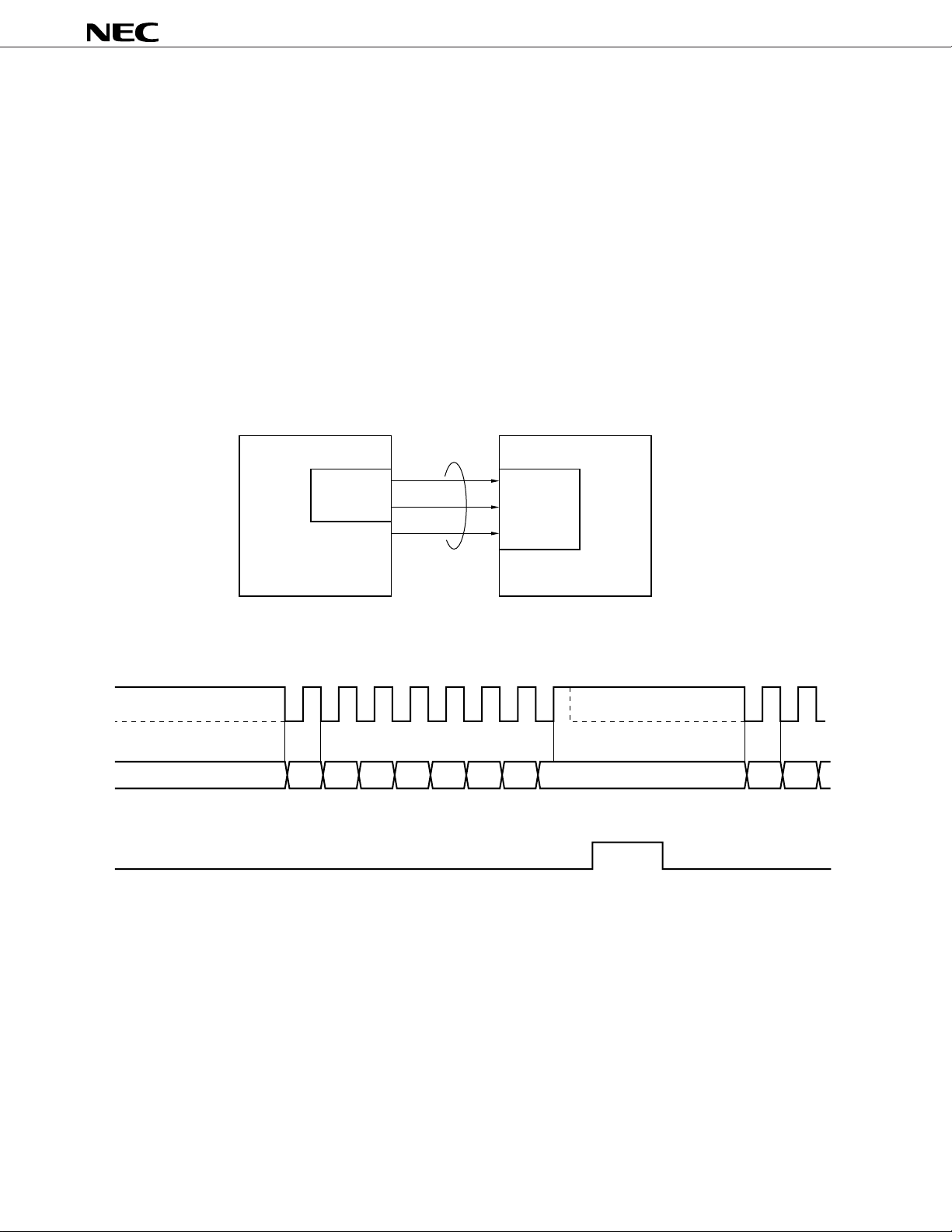
2.1.7 Microcontroller Interface
The µPD9930 can control internal functions by microcontroller command. A clock synchronous serial I/O is
incorporated to receive command.
A clocked serial interface is provided to receive microcontroller commands. A microcontroller connection
example is shown in Figure 2-9. 8-bit length data is received by the serial clock (MCLK), serial input (MDAT),
Note
and strobe input (MSTR) lines
.
The timing chart is shown in Figure 2-10. By reading data to the internal shift register and setting MSTR
to high level at the MCLK rising point, it is latched to the internal control register. Data transfer must be made
with LSB first.
Note When 8 bits or more (9 MCLK clocks or more) data is input, the last 8-bit which is input immediately before
the active edge of MSTR is recognized as a control command.
Figure 2-9 Example of Connection with Microcontroller
PD9930
Microcontroller
µ
MCLK
MDAT
MSTR
Serial I/O
SO
SCK
PORT
Microcontroller I/F
MDAT
MCLK
MSTR
Figure 2-10 Microcontroller Interface Timing Chart
D0 D1 D2 D3 D4 D5 D6 D7 D0 D1
18

µ
g
PD9930
2.1.8 DSP Interface
A clock synchronous serial I/O is built-in to exchange voice send/receive coding data with an external DSP.
16-bit data is transferred at 8 kHz by the serial clock (SCLK = 256 kHz), serial input (SI), serial output (SO),
and enable output (SEN) lines. The REQB is a terminal for allowing/inhibiting data transmission. There are
two modes for data input and output timing, and either can be selected by the DSPSEL terminal. Select the
mode matching the DSP serial interface input/output timing. Data format is as follows: Both SO output and SI
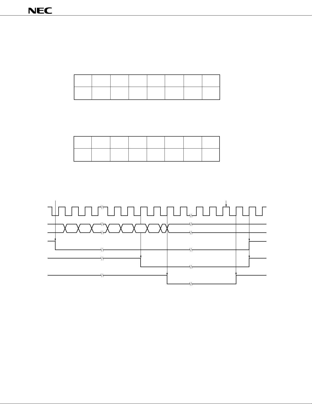
input are in 2's complement format with MSB first.
Figure 2-11 Data Format in DSP Interface
D15 D14 D13 D12 D11 D10 D9 D8 D7 D6 D5 D4 D3 D2 D1 D0SO output
Coding data (13 bits)
Sign bit Invalid data
Remark A full code is output when the SO pin is +3.17 dBm0 (A/D 1.2 V
D15 D14 D13 D12 D11 D10 D9 D8 D7 D6 D5 D4 D3 D2 D1 D0SI input
Coding data (15 bits)
Si
n bit
p-p).
Remark When a full code is input to the SI pin, the accessory output is 1.2 V
Table 2-5 DSP Input/Output Timing Mode Selection
Pin input
DSPSEL
H MODE1
L MODE2
Mode
Table 2-6 Allowing Data Transmission
REQB pin Input Data Transmission
L Data transmission is allowed. Enable signal (SEN) is output at rising edge of FSYNC (8 kHz), and
data input/output is started.
H Enable signal is not output and data are not input or output.
p-p.
19
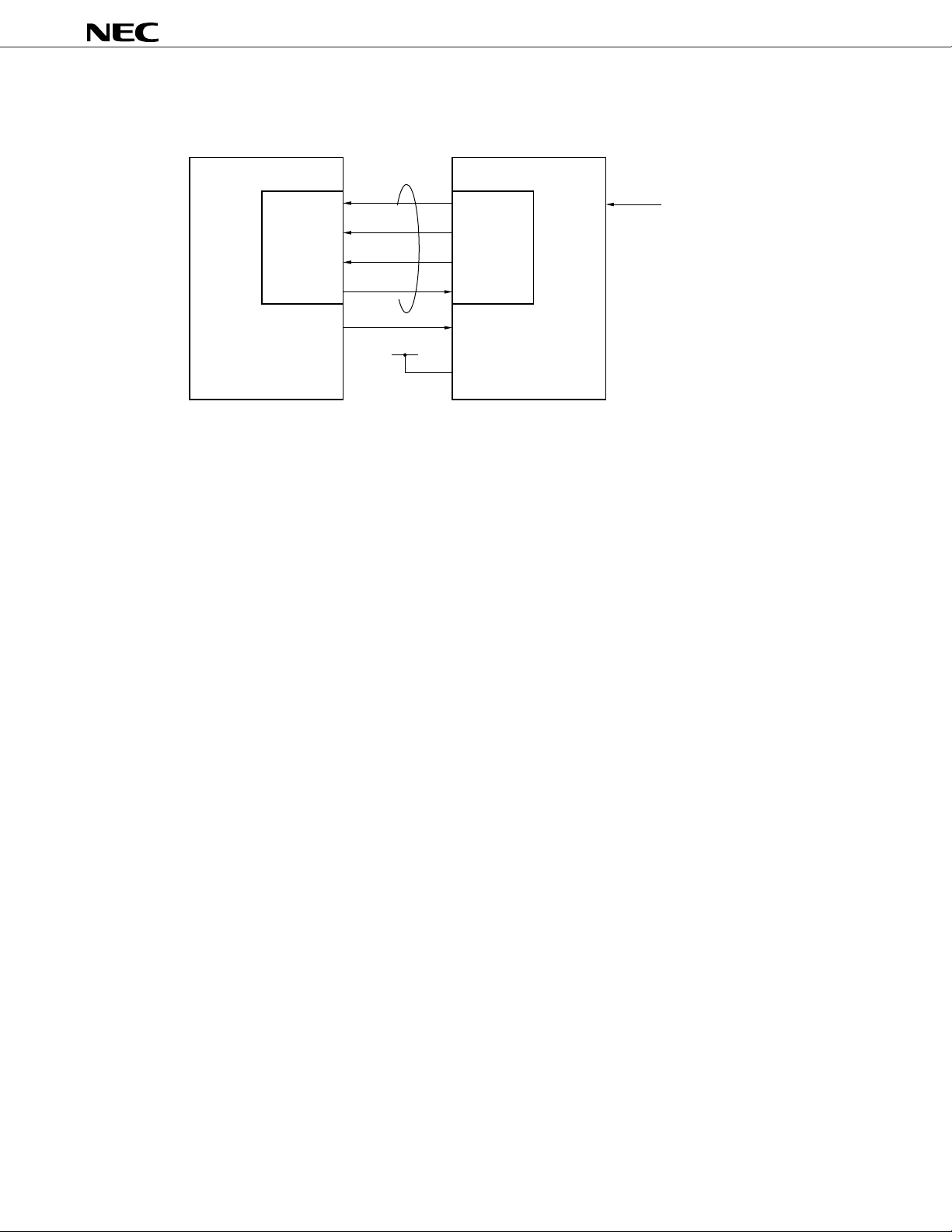
Figure 2-12 Example of Connection with DSP (Mode 1)
µ
DSP
PD9930
µ
PD9930
Serial I/O
SCK
enable
SI
SO
PORT
V
DD
Note When using with mode 2, connect DSPSEL to GND.
DSP I/F
SCLK
SEN
SO
SI
REQB
DSPSEL
Note
FSYNC
8 kHz
20
REQB
FSYNC
(8 kHz)
SEN
SCLK
(256 kHz)
SO
SI
125 s
D15 D14 D2 D1 D0 D15 D14
D15 D14 D2 D1 D0 D15 D14D13
D13
µ
D13
D12
don't care don't care
Figure 2-13 DSP Interface Timing Chart
µ
PD9930
REQB
FSYNC
(8 kHz)
SEN
SCLK
(256 kHz)
SO
SI
don't care
(a) Mode 1 (DSPSEL = V
125 s
µ
D15 D14 D2 D1 D0 D15 D14
D15 D14 D2 D1 D0 D15 D14
DD)
don't care
D13
D13
(b) Mode 2 (DSPSEL = GND)
21
µ
PD9930
2.1.9 DAI (Digital Audio Interface)
Has a on-chip circuit enabling DAI functions specified in GSM11.10. The receive system has a on-chip LPF
only. If a BPF is necessary, it should be mounted externally. System configuration at the time of DAI test mode
is shown in Figure 2-15. The DAI terminal is connected to the system simulator via the pin 25 DSUB socket.
The test mode can be selected by terminals TC1 or TC2, or by microcontroller command. DAI mode should be
set after completing power-up operation (30.5 ms after executing power-up command).
When changing the modes from DAI to normal, either of the following operations should be executed.
• After specifying normal mode, input the DAI reset signal (DRSTB = low).
• Input reset signal (RESETB = low).
When specifying by command, test control register mode specification bits (ITC1, ITC2) are used (Refer to
4.4.1 Test Control Register (TSTCR).).
Timing for each mode is shown in Figures 2-16 through 2-20.
For operation at the time of each mode, refer to Figure 4-13 Test Mode Operation.
Table 2-7 DAI Test Mode Specification
TC2 TC1 Test mode Function
(ITC2) (ITC1) specification
0 0 Normal operation
0 1 Speech encoder Outputs data input from DI pin to DSP (speech encoder) from SO pin.
test mode Input is started at rising edge of first FSYNC (8-kHz external clock input) after
1 0 Speech decoder Outputs speech decoder output data input from SI pin from DO pin.
test mode Inputting data from DSP is started at rising edge of first FSYNC (8-kHz external
1 1 Acoustic device, A/D, Outputs audio data converted into digital signal from DO pin.
D/A test mode Also inputs audio data input from DI pin to D/A converter. Inputting/outputting data
Note
Normal operation.
This mode is set at system reset (when RESETB = low) regardless of status of TC1
and TC2.
execution of mode specification, and outputting data to DSP is started at next rising
edge of FSYNC.
clock input) after execution of mode specification, and data is output from DO pin at
next rising edge of FSYNC.
is started at rising edge of first FSYNC (8-kHz external clock input) after execution
of mode specification. At this time, clock output to DSP (SCLK) is stopped.
Note In the normal mode, do not set DRSTB to low level (during low period, serial interface with DSP is disabled).
As well, set the output pins of driver IC to high-impedance state, because DRSTB input pin is connected with
a pull-up resistor.
Remark Analog loop back mode and DAI test mode cannot be specified at the same time.
DAI test mode is set with TC1, TC2 (or ITC1, ITC2) and DRSTB pins. DAI test mode is entered at the rising
edge of the DRSTB signal when both TC1 and TC2 pins (or ITC1 and ITC2 pins) are set as shown in Figure
2-14.
22
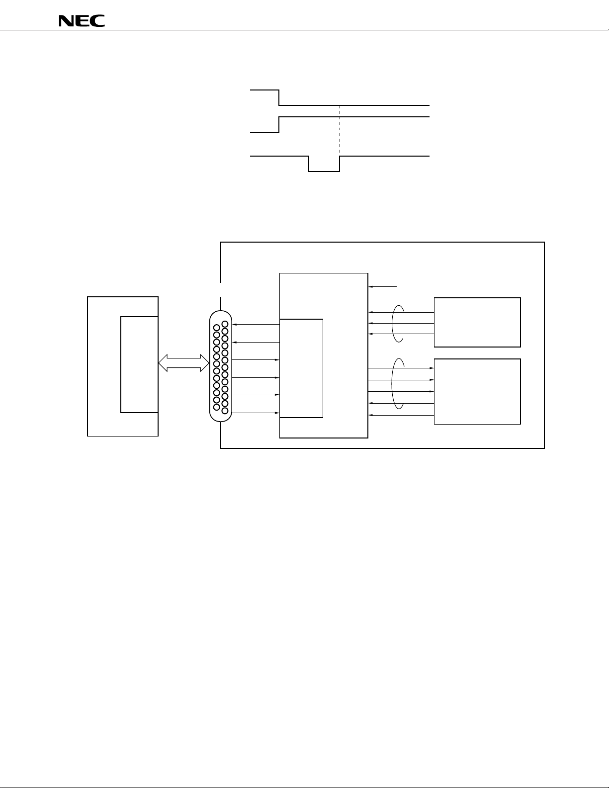
Figure 2-14 Latch Timing of TC1, TC2 (or ITC1, ITC2)
TC1 (ITC1)
TC2 (ITC2)
DRSTB
Figure 2-15 Example of System Configuration at Time of DAI Test Mode
Mobile equipment
PD9930
µ
µ
PD9930
8 kHz
Test command
Microcontroller
DSP
(SP-CODEC)
DAI
25-Pin DSUB socketSystem simulator
DAI
DCLK
DO
DI
TC1
TC2
DRSTB
FSYNC
MCLK
MSTR
MDAT
SCLK
SEN
SO
SI
REQB
Remark In the acoustic device test mode, REQB is ignored (both high and low levels). When DSPSEL = VDD (mode
1), SCLK and SEN are fixed to low, and when DSPSEL = GND (mode 2), fixed to high.
23
24
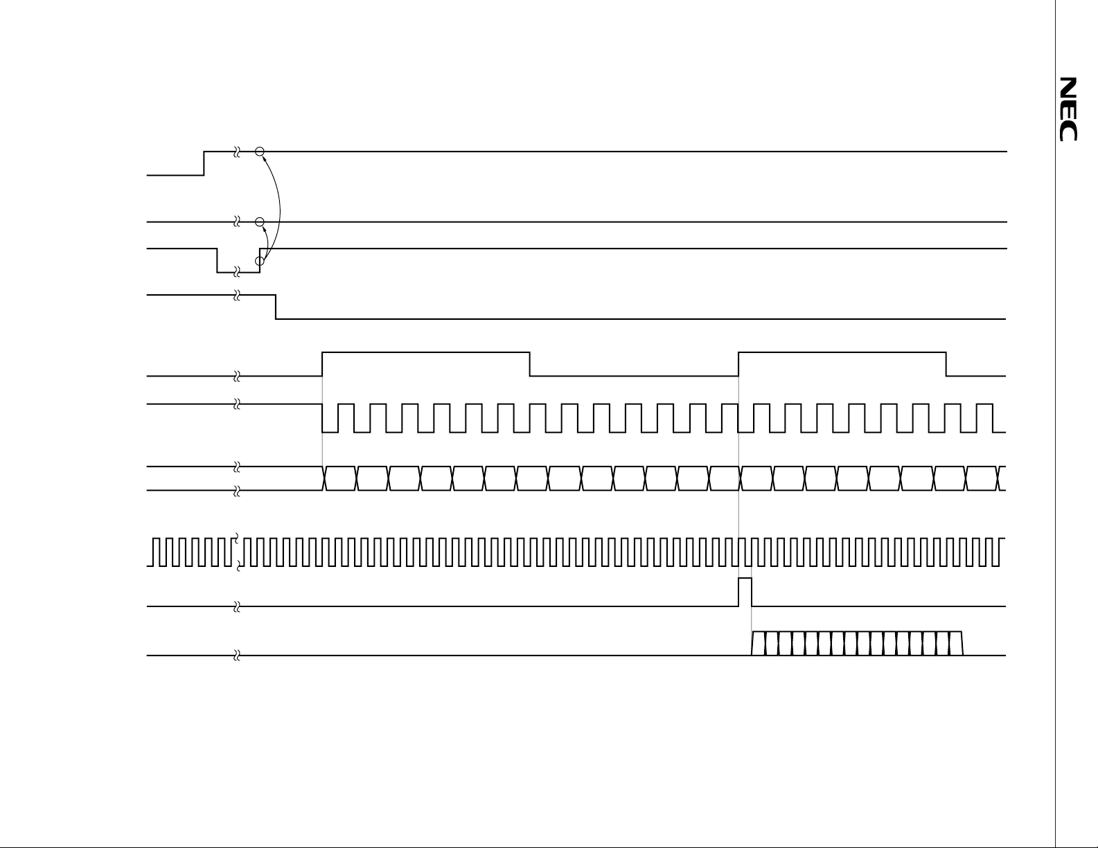
Figure 2-16 Speech Encoder Test Mode (DSP Interface = MODE 1) (TC1 = 1, TC2 = 0)
TC1 (ITC1)
TC2 (ITC2)
DRSTB
REQB
FSYNC
(8 kHz)
DCLK
(104 kHz)
DI
SCLK
(256 kHz)
SEN
don't care
"L"
D12 D11 D10 D9 D8 D7 D6 D5 D4 D3 D2 D1 D0 D12 D11 D10 D9 D8 D7 D6 D5
SO
D14 D13 D12 D11 D10 D9 D8 D7 D6 D5 D4 D3 D2 D1 D0
D15
µ
PD9930
 Loading...