NEC UPD9903GT Datasheet

DATA SHEET
MOS INTEGRATED CIRCUIT
µ
PD9903
µ
PD9903 ANALOG SUBSCRIBER LINE LSI (DIGITAL CODEC)
The µPD9903 is a digital CODEC that can be used in analog subscriber circuits such as private branch exchangers
(PBXs) and switching equipment for central offices. It features three of the functions required for analog subscriber
circuits: 2W/4W conversion, CODEC supervision, and subscriber line supervision.
µ
Use of the
in analog subscriber circuits.
FEATURES
• Single-chip monolithic LSI (CMOS)
• PCM CODEC → oversampling-type A/D and D/A converters
• Programmable functions
• Termination impedance
• Hybrid balance network
• Feed resistance
• Feed current
• PAD control
• A-law and
• Digital gain set function
• Ring-Trip function
• Single power supply (+5 V)
• Low power consumption during standby mode: 20 mW (TYP.)
PD9903 in combination with a BS-SLIC (µPC7073) can reduce the number of components required
µ
-law
ORDERING INFORMATION
Part Number Package
µ
PD9903GT 48-pin plastic shrink SOP (375 mil)
The information in this document is subject to change without notice.
Document No. S10897EJ3V0DS00 (3rd edition)
Date Published June 1997 N
Printed in Japan
The mark shows major revised points.
©
1996

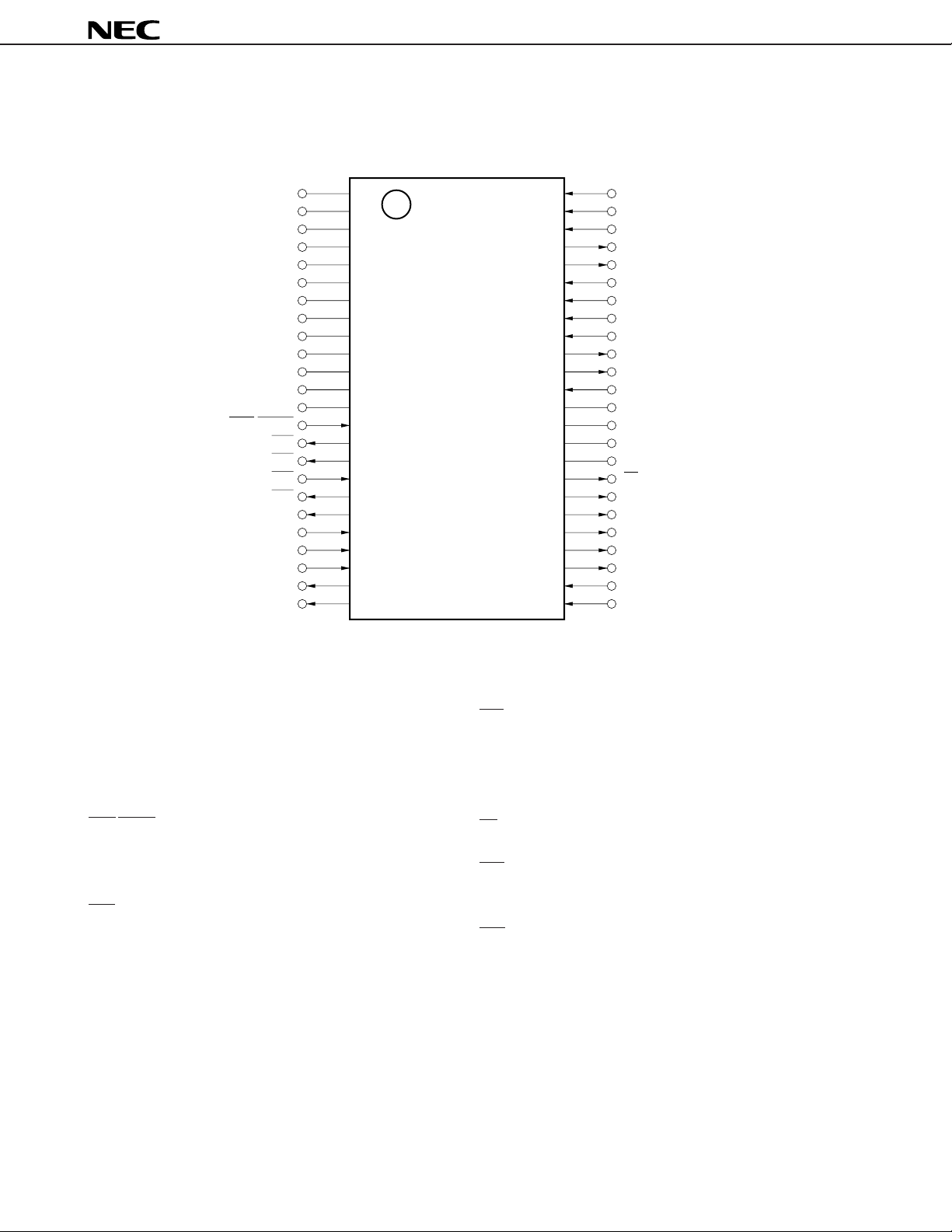
PIN CONFIGURATION (Top View)
48-pin plastic shrink SOP (375 mil)
µ
PD9903
NC
NC
NC
NC
NC
NC
NC
NC
NC
NC
AV
DV
DD1
DV
DD2
AUX/MODE
BSY
SUS
RST
EXS
EXD
HW
DCLK
FS
HW
TYPE
1
2
3
4
5
6
7
8
9
10
DD
11
µ
PD9903GT
12
13
14
15
16
17
18
19
R
20
21
22
X
23
24
48
47
46
45
44
43
42
41
40
39
38
37
36
35
34
33
32
31
30
29
28
27
26
25
DC
IN3
DC
IN2
DC
IN1
DC
OUT1
DC
OUT2
BB
IN
ASCN
AGDT
A
IN
A
OUT
ACOM
ACOM
AGND
SUB
DGND1
DGND2
PD
ALM
BCUT
1
RC
RC
2
RC
3
RT
IN0
RT
IN1
OUT
IN
ACOMIN : ANALOG COMMON VOLTAGE IN DGND1, DGND2: DIGITAL GROUND
ACOMOUT : ANALOG COMMON VOLTAGE OUT DVDD1, DVDD2 : DIGITAL POSITIVE POWER SUPPLY
AGDT : ANALOG GROUND DETECTION SIGNAL IN EXD : EXPANSION PORT DATA
AGND : ANALOG GROUND EXS :
EXPANSION PORT SYNCHRONIZATION
AIN : ANALOG SIGNAL IN FS : FRAME SYNCHRONOUS CLOCK IN
ALM : ALARM OUT HW
R : RECEIVE HIGHWAY DATA IN
AOUT : ANALOG SIGNAL OUT HWX : TRANSMIT HIGHWAY DATA OUT
ASCN : ANALOG LOOP DETECTION SIGNAL IN NC : NO CONNECTION
AUX/MODE : EXTERNAL SIGNAL IN/MODE CONTROL SET PD : POWER DOWN CONTROL OUT
DD : ANALOG POSITIVE POWER SUPPLY RC1 - RC3 : RELAY CONTROL OUT
AV
BBIN :VBB VOLTAGE INFORMATION IN RST : RESET IN
BCUT : BATTERY FEED CUT SIGNAL OUT RT
IN0, RTIN1 : RING TRIP SIGNAL IN
BSY : BUSY SIGNAL OUT SUB : SUB GROUND
DCIN1 - DCIN3 : DC FEEDBACK CONTROL IN SUS : SUSPEND SIGNAL OUT
DCLK : DATA CLOCK IN TYPE : TYPE SIGNAL OUT
OUT1, DCOUT2 : DC FEEDBACK CONTROL OUT
DC
2

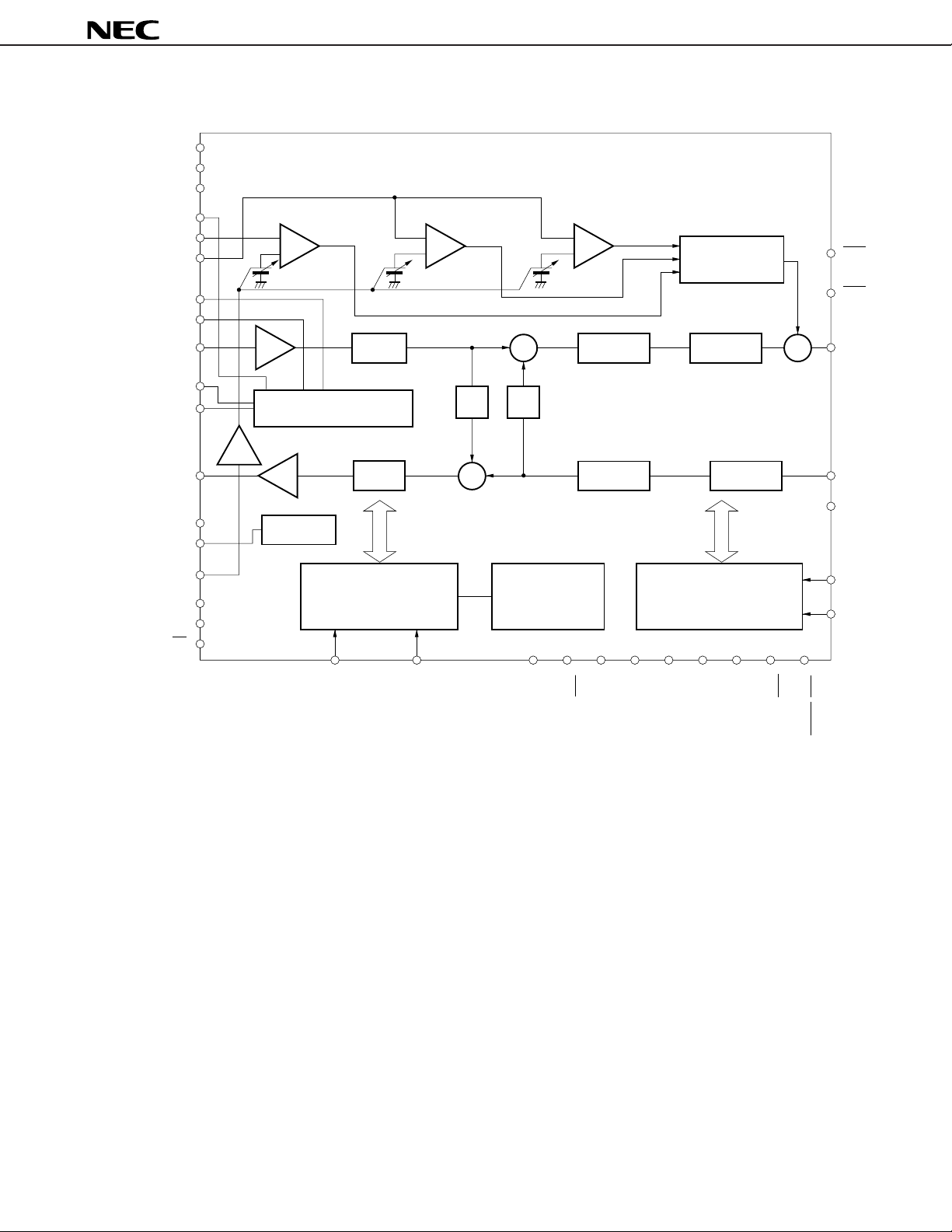
BLOCK DIAGRAM
RC
1
RC
2
RC
3
DC
IN1
ASCN
AGDT
IN2
DC
DC
IN3
A
IN
DC
OUT1
DC
OUT2
A
OUT
ACOM
IN
ACOM
OUT
COMP. COMP. COMP.
+
H
Z
B
Feed control
Reference
voltage
A/D
D/A
H
+
Channel
filter
Channel
filter
SUS
GDT
Waveform shaping
guard processing
SCN
Linear to
m
A or
A or to
linear
µ
PD9903
µ
BSY
SUS
+
HW
HW
X
R
TYPE
BB
BCUT
ALM
PD
IN
FS
Controller Ring-Trip Timing
DCLK
RT
IN0
RT
IN1
EXD
EXS
SUB
AGND
DGND
AVDDDVDDRST
AUX/MODE
3

µ
PD9903
CONTENTS
1. PIN FUNCTIONS ...................................................................................................................... 5
2. USE CAUTIONS ....................................................................................................................... 7
3. ELECTRICAL SPECIFICATIONS ........................................................................................... 8
3.1 Discrete unit Ratings...................................................................................................................... 8
3.2 Combined Specifications with the µPC7073 ............................................................................. 17
4. SYSTEM APPLICATION EXAMPLE USING THE µPC7073 AND µPD9903............. 21
5. PACKAGE DRAWING ............................................................................................................. 22
6. RECOMMENDED SOLDERING CONDITIONS ................................................................... 23
4

µ
1. PIN FUNCTIONS
Number Pin Name I/O Function
1-10 NC – Leave this pin open.
11 AV DD – +5 V power supply (analog)
12 DVDD1 – +5 V power supply (digital)
13 DVDD2 – +5 V power supply (digital)
14 AUX/MODE I External signaling input
15 BSY O BUSY LED driver output
16 SUS O SUS LED driver output
17 RST I Pin for reset input and power-on reset
H: HWX valid, L: HWX output’s internal F/F clear status
18 EXS O SIPO sync signal output for expansion port
19 EXD O SIPO serial data output for expansion port
20 HWR I Reception highway input [PCM data (8-bit) + CTL data (8-bit)]
21 DCLK I Clock input (2.048 MHz)
22 FS I 8-kHz sync input Rising: HWR PCM data input start
Rising: HWX PCM data output start
Falling: HWR CTL data input start
Falling: HWX SCN data output start
23 HWX O Transmission highway output [PCM data (8-bit) + SCN data (8-bit)]
24 TYPE O HWX data enable
25 RT IN1 I Ring-Trip signal input 2
26 RT IN0 I Ring-Trip signal input 1
27 RC3 O Relay control for network testing [to the µPC7073’s pin 22]
28 RC2 O Relay control for line testing [to the µPC7073’s pin 21]
29 RC1 O Relay control for ringer transmit [to the µPC7073’s pin 20]
30 BCUT O High and wet control output [to the µPC7073’s pin 19]
31 ALM O Control output for ground-fault/power line contact protection mode
32 PD O Power-down control output [to the µPC7073’s pin 17]
33 DGND2 – Digital ground 2
34 DGND1 – Digital ground 1
35 SUB – Substrate ground
36 AGND – Analog ground
37 ACOM IN I Signal ground input
38 ACOM OUT O Signal ground output
39 AOUT O Analog signal output for receive side [to the µPC7073’s pin 10]
40 AIN I Analog signal input for transmit side [to the µPC7073’s pin 9]
41 AGDT I Tip-Ring sum current detection input [to the µPC7073’s pin 8]
42 ASCN I Tip-Ring difference current detection input [to the µPC7073’s pin 7]
43 BB IN IVBB voltage information input [to the µPC7073’s pin 6]
Note 2
Note 2
Note 2
Note 2
Note 3
Note 3
Note 1
Note 1
[to the µPC7073’s pin 18]
[to the µPC7073’s pin 11]
[to the µPC7073’s pin 11]
PD9903
Notes 1. SIPO: Serial In Parallel Out
2. Short AGND, DGND1, DGND2, and SUB directly under the IC and connect them to an analog ground.
3. Short ACOM
IN and ACOMOUT directly under the IC.
5

Number Pin Name I/O Function
44 DCOUT2 O DC feedback bias voltage output [to the µPC7073’s pin 5]
45 DCOUT1 O DC feedback control output [to the µPC7073’s pin 4]
46 DCIN1 I DC feedback control input 1 [to the µPC7073’s pin 3]
47 DCIN2 I DC feedback control input 2 [to the µPC7073’s pin 2]
48 DCIN3 I DC feedback control input 3 [to the µPC7073’s pin 1]
µ
PD9903
6

µ
PD9903
2. USE CAUTIONS
(1) Combined characteristics of the µPC9903 and µPD7073
• The µPD9903 is designed to be used in combination with the µPC7073. Therefore, the first half of the electrical
µ
specifications described below are ratings for the
combined ratings with the µPC7073.
• Subscriber circuit constants that are determined by factors such as termination impedance are configured to
enable setting by external order parameters. Consequently, input of an order that is not suitable for the target
impedance may result in failure to obtain the required characteristics.
(2) Absolute maximum ratings
Application of voltage or current in excess of the absolute maximum ratings may result in damage. Be
especially cautious about surges, etc.
(3) Load of by-pass capacitor
µ
Because the
supply impedance can cause instability in these internal operational amplifiers (such as oscillation). To
suppress such instability and eliminate power supply noise, connect by-pass capacitors (CACOM = approximate
µ
F) having superior high frequency characteristics as close as possible to the µPC7073’s power supply
0.1
pins (VBB and VCC) and the µPD9903’s power supply pins (AVDD and DVDD).
PC7073 and µPD9903 use several internal high-frequency operational amplifiers, high power
PD9903 as a discrete unit while the second half are
(4) Addition of ACOM pin connection capacitor
µ
The voltage of the ACOM pin between the
source between the µPC9903 and µPC7073. Superposing of noise on this pin may have adverse effects
on transmission characteristics. Therefore, make the wires between the ACOM pins of the two LSIs as short
as possible, and connect capacitors (C
characteristics as close as possible to the pins.
PC7073 and µPD9903 is the reference voltage of the signal
ACOM = approximate 0.1
µ
F) having superior high frequency
7

3. ELECTRICAL SPECIFICATIONS
3.1 Discrete unit Ratings
Absolute maximum ratings (TA = +25 °C)
Parameter Symbol Conditions Rating Units
Power supply voltage VDD AVDD, DVDD1, DVDD2 –0.3 to +7.0 V
Analog input voltage VAIN AIN, ASCN, AGDT, ACOMIN, BBIN, –0.3 to VDD + 0.3
DCIN1, DCIN2, and DCIN3 pins
Digital input voltage VDIN HWR, DCLK, FS, RST, AUX/MODE, –0.3 to VDD + 0.3
RTIN0, and RTIN1 pins
Applied voltage to analog VAOUT AOUT, DCOUT1, DCOUT2, and ACOMOUT –0.3 to VDD + 0.3
output pin pins
Applied voltage to digital VDOUT HWX, BSY, SUS, RC1, RC2, RC3, EXS, –0.3 to VDD + 0.3
output pin EXD, BCUT, ALM, PD, and TYPE pins
Power dissipation PT 500 mW
Ambient operating temperature
Storage temperature T stg –65 to +150
TA 0 to +70 ˚C
µ
PD9903
Caution If the absolute maximum rating for any of the above parameters is exceeded even momentarily,
it may adversely affect the quality of this product. In other words, these absolute maximum
ratings have been set to prevent physical damage to the product. Do not use the product in such
a way as to exceed any of these ratings.
Recommended operating conditions (T
A = 0 to 70 °C, VDD = 5 V ± 5 %, GND = 0 V)
(1) DC conditions
Parameter Symbol Conditions MIN. TYP. MAX. Units
Ambient operating temperature
Power supply voltage VDD 4.75 5.0 5.25 V
Analog input voltage VAI ASCN, and AGDT pins 0 VDD
Analog input driving
resistance
Analog output load resistance
Analog output load capacitance
Low level input voltage VIL1 FS, DCLK, HWR, and AUX/MODE pins 0 0.8 V
High level input voltage VIH1 FS, DCLK, HWR, and AUX/MODE pins 2.0 VDD
TA 0 2570˚C
RLA1 ASCN, and AGDT pins 20 kΩ
RLOAD AOUT pin 100
CLOAD 100 pF
VIL2 RST, RTIN0, and RTIN1 pins 0 0.2 × VDD
VIH2 RST, RTIN0, and RTIN1 pins 0.8 × VDD VDD
8

µ
PD9903
(2) AC conditions
Parameter Symbol Conditions MIN. TYP. MAX. Units
Data clock frequency fDCLK (= 1/tCY) ± 50 ppm 2048 kHz
Data clock pulse width tDCLK 200 ns
Frame sync clock frequency fS ± 50 ppm 8.0 kHz
High level frame sync pulse tWHS tCY × 8ns
width
Low level frame sync pulse tWLS tCY × 8ns
width
Clock rise time tR 30 ns
Clock fall time tF 30 ns
Float in sync timing tCSD1 100 ns
tCSD2 40 ns
High level width of frame tWHSC 100 ns
sync clock and data clock
HWR set-up time tDSR Note 1 65 ns
HWR hold time tDHR Note 1 120 ns
Minimum width of reset pulse
PWRST RST pin
Note 2
10
µ
s
Notes 1. During timing measurement, use 5 ns as the rise time and fall time for the digital input wave form and
clock signal.
µ
2. The
PD9903 is initialized when high level input is applied to the RST pin after applying low level input
for several clock widths. (However, use of the RST pin is not guaranteed during low level input. Also,
µ
low level input alone does not initialize the
PD9903.)
9
 Loading...