
DATA SHEET
MOS INTEGRATED CIRCUIT
µ
PD78P4908
16-BIT SINGLE-CHIP MICROCONTROLLER
DESCRIPTION
The µPD78P4908, 78K/IV series' product, is a one-time PROM version of the µPD784907 and µPD784908 with
internal mask ROM.
Since user programs can be written to PROM, this microcomputer is best suited for evaluation in system
development, manufacture of small quantities of multiple products, and fast start-up of applications.
For specific functions and other detailed information, consult the following user's manuals.
These manuals are required reading for design work.
µ
PD784908 Subseries User's Manual - Hardware : U11787E
78K/IV Series User's Manual - Instruction : U10905E
FEATURES
• 78K/IV series
• Internal PROM: 128 Kbytes
• Internal RAM: 4,352 bytes
• Supply voltage: VDD = 4.5 to 5.5 V
(At main clock: f
V
DD = 4.0 to 5.5 V
(Other than above: f
ORDERING INFORMATION
Part number Package Internal ROM
µ
PD78P4908GF-3BA 100-pin plastic QFP (14 × 20 mm) One-time PROM
XX = 12.58 MHz, internal system clock = fXX: fCYK = 79 ns)
CYK = 159 ns)
The information in this document is subject to change without notice.
Document No. U11681EJ2V0DS00 (2nd edition)
Date Published February 1999 N CP(K)
Printed in Japan
The mark shows major revised points.
©
1996
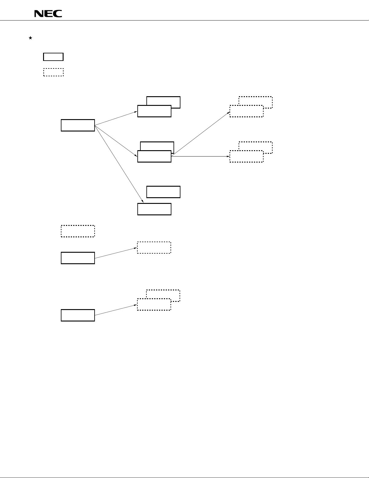
78K/IV SERIES PRODUCT DEVELOPMENT DIAGRAM
: Under mass production
: Under development
µ
PD78P4908
Standard models
PD784026
µ
Enhanced A/D,
16-bit timer,
and power
management
ASSP models
PD784955
µ
For DC inverter control
PD784908
µ
Equipped with IEBus
controller
I2C bus supported
PD784038Y
µ
PD784038
µ
Enhanced internal memory capacity,
pin compatible with the PD784026
µ
PD784216Y
µ
PD784216
100 pins,
enhanced I/O and
internal memory capacity
µ
PD784054
µ
PD784046
Equipped with 10-bit A/D
PD784938
µ
Enhanced function of the PD784908,
TM
enhanced internal memory capacity,
added ROM correction
µ
µ
Multimaster I2C bus supported
PD784225Y
µ
PD784225
µ
80 pins,
added ROM correction
Multimaster I2C bus supportedMultimaster I2C bus supported
PD784218Y
µ
PD784218
µ
Enhanced internal memory capacity,
added ROM correction
µ
PD784915
For software servo control,
equipped with analog circuit
for VCR,
enhanced timer
Multimaster I2C bus supported
PD784928Y
µ
PD784928
µ
Enhanced function of the PD784915
µ
2
Data Sheet U11681EJ2V0DS00
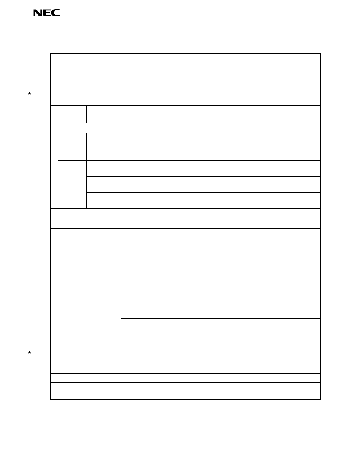
FUNCTIONS
µ
PD78P4908
(1/2)
Item
Number of basic instructions
(mnemonics)
General-purpose register
Minimum instruction execution
time
Internal
memory
Memory space
I/O ports
Additional
function
Note
pins
Real-time output ports
IEBus controller
Timer/counter
Clock timer
Clock output
PWM outputs
Serial interface
ROM
RAM
Total
Input
Input/output
LED direct
drive outputs
Transistor
direct drive
N-ch open
drain
Function
113
8 bits × 16 registers × 8 banks, or 16 bits × 8 registers × 8 banks (memory mapping)
• 320 ns/636 ns/1.27
• 160 ns/320 ns/636 ns/1.27
128 Kbytes
4,352 bytes
Program and data: 1 Mbyte
80
8
72
24
8
4
4 bits × 2, or 8 bits × 1
Incorporated (simple version)
Timer/counter 0: Timer register × 1 Pulse output capability
(16 bits) Capture register × 1 • Toggle output
Timer/counter 1: Timer register × 1 Real-time output port
(16 bits) Capture register × 1
Timer/counter 2: Timer register × 1 Pulse output capability
(16 bits) Capture register × 1 • Toggle output
Timer 3: Timer register × 1
(16 bits) Compare register × 1
Interrupt requests are generated at 0.5-second intervals. (A clock timer oscillator is
incorporated.)
Either the main clock (6.29 MHz/12.58 MHz) or real-time clock (32.768 kHz) can be
selected as the input clock.
Selected from fCLK, fCLK/2, fCLK/4, fCLK/8, or fCLK/16 (can be used as a 1-bit output port)
12-bit resolution × 2 channels
UART/IOE (3-wire serial I/O) : 2 channels (incorporating baud rate generator)
CSI (3-wire serial I/O) : 2 channels
µ
s/2.54 µs (at 6.29 MHz)
µ
s (at 12.58 MHz)
Compare register × 2 • PWM/PPG output
• One-shot pulse output
Capture/compare register × 1
Compare register × 1
Capture/compare register × 1 • PWM/PPG output
Compare register × 1
Note Additional function pins are included in the I/O pins.
Data Sheet U11681EJ2V0DS00
3
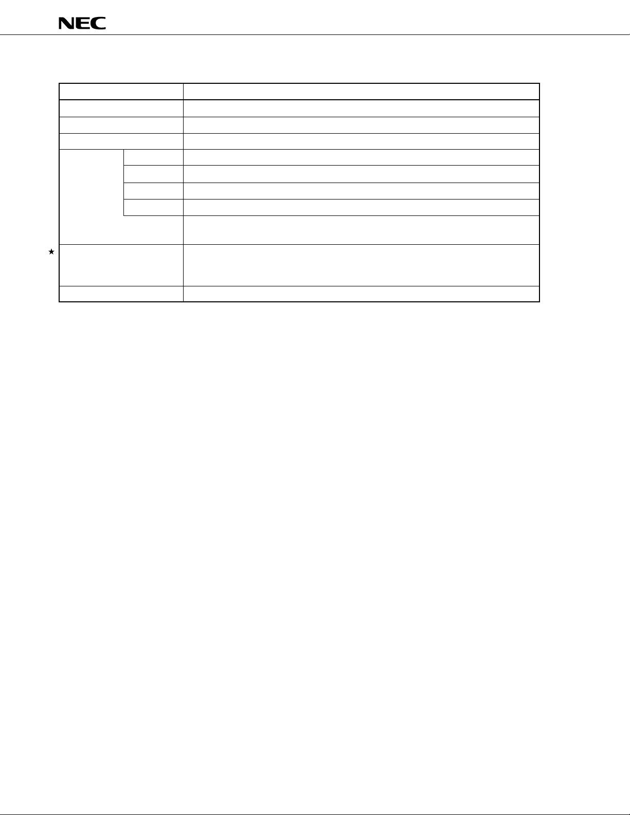
µ
PD78P4908
(2/2)
Item
A/D converter
Watchdog timer
Standby
Interrupt
Power supply voltage
Package
Hardware source
Software source
Nonmaskable
Maskable
Function
8-bit resolution × 8 channels
1 channel
HALT/STOP/IDLE mode
27 (20 internal, 7 external (sampling clock variable input: 1))
BRK or BRKCS instruction, operand error
1 internal, 1 external
19 internal, 6 external
• 4-level programmable priority
• 3 operation statuses: vectored interrupt, macro service, context switching
• VDD = 4.5 to 5.5 V (At main clock: fXX = 12.58 MHz, internal system clock = fXX: fCYK =
79 ns)
• VDD = 4.0 to 5.5 V (Other than above: fCYK = 159 ns)
100-pin plastic QFP (14 × 20 mm)
4
Data Sheet U11681EJ2V0DS00

µ
PD78P4908
CONTENTS
1. DIFFERENCES BETWEEN µPD78P4908 AND MASK ROM PRODUCTS ............................ 6
2. PIN CONFIGURATION (TOP VIEW) ......................................................................................... 7
3. BLOCK DIAGRAM ..................................................................................................................... 1 0
4. PIN FUNCTIONS ........................................................................................................................ 1 1
4.1 PINS FOR NORMAL OPERATING MODE.................................................................................... 11
4.2 PINS FOR PROM PROGRAMMING MODE (V
4.2.1 Pin Functions ................................................................................................................. 14
4.2.2 Pin Functions ................................................................................................................. 15
4.3 I/O CIRCUITS FOR PINS AND HANDLING OF UNUSED PINS ................................................. 16
PP ≥ +5 V or +12.5 V, RESET = L) .................... 14
5. INTERNAL MEMORY SIZE SELECT REGISTER (IMS).......................................................... 19
6. PROM PROGRAMMING ............................................................................................................ 20
6.1 OPERATION MODE........................................................................................................................ 20
6.2 PROM WRITE SEQUENCE ............................................................................................................ 2 2
6.3 PROM READ SEQUENCE ............................................................................................................. 26
7. SCREENING ONE-TIME PROM PRODUCTS .......................................................................... 26
8. ELECTRICAL CHARACTERISTICS ......................................................................................... 27
9. PACKAGE DRAWING ................................................................................................................ 51
10. RECOMMENDED SOLDERING CONDITIONS ........................................................................ 52
APPENDIX A DEVELOPMENT TOOLS .......................................................................................... 53
APPENDIX B CONVERSION SOCKET (EV-9200GF-100) PACKAGE DRAWING ..................... 56
APPENDIX C RELATED DOCUMENTS ......................................................................................... 58
Data Sheet U11681EJ2V0DS00
5

µ
PD78P4908
1. DIFFERENCES BETWEEN µPD78P4908 AND MASK ROM PRODUCTS
The µPD78P4908 is produced by replacing the mask ROM in the µPD784907 or µPD784908 with PROM to which
µ
data can be written. The functions of the
for the PROM specification such as writing and verification, except that the PROM size can be changed to 96 or 128
Kbytes, and except that the internal RAM size can be changed to 3,584 or 4,352 bytes.
Table 1-1 shows the differences between these products.
Table 1-1. Differences Between the
PD78P4908 are the same as those of the µPD784907 or µPD784908 except
µ
PD78P4908 and Mask ROM Products
Product name
Item
Internal program
memory
Internal RAM
Pin connection
Power supply voltage
Electrical
characteristics
µ
µ
PD78P4908
• 128-Kbyte PROM
• 96-Kbyte mask ROM
PD784907
µ
PD784908
• 128-Kbyte mask ROM
• Can be changed to 96
Kbytes by IMS
• 4,352-byte internal RAM
• 3,584-byte internal RAM
• 4,352-byte internal RAM
• Can be changed to 3,584
bytes by IMS
Pin functions related to writing or reading of PROM have been added to the µPD78P4908.
• VDD = 4.5 to 5.5 V • VDD = 4.0 to 5.5 V
(At main clock: fXX = 12.58 (At main clock: fXX = 12.58 MHz, internal system clock = fXX:
MHz, internal system clock = fCYK = 79 ns)
fXX: fCYK = 79 ns • VDD = 3.5 to 5.5 V
• VDD = 4.0 to 5.5 V (Other than above: fCYK = 159 ns)
(Other than above: fCYK =
159 ns)
Partially differs between these products.
6
Data Sheet U11681EJ2V0DS00
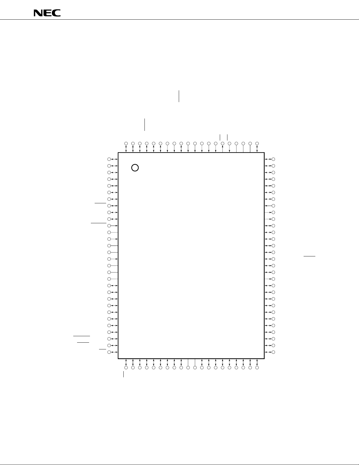
2. PIN CONFIGURATION (TOP VIEW)
(1) Normal operation mode
• 100-pin plastic QFP (14 × 20 mm)
µ
PD78P4908GF-3BA
P35/TO1
P34/TO0
P33/SO0
P32/SCK0
100
99
98
97
96
P37/TO3
P100
Note 2
Note 3
2
3
4P101
5P102
6P103
7P104
8P105/SCK3
9P106/SI3
10P107/SO3
11RESET
12XT2
13XT1
14V
SS
15X2
16X1
17REGOFF
18REGC
19VDD
20P00
21P01
22P02
23P03
24P04
25P05
26P06
27P07
28P67/REFRQ/HLDAK
29P66/WAIT/HLDRQ
30P65/WR
31 32 33 34 35 36 37 38 39 40 41 42 43 44 45 46 47 48 49 50
P31/TxD/SO1
P30/RxD/SI1
P27/SI094P26/INTP5
95
93
92
P25/INTP4/ASCK/SCK1
P24/INTP3
P23/INTP2/CI
P22/INTP1
P21/INTP0
P20/NMI87TX86RX85AVSS84AVREF183AVDD82P77/ANI7
91
90
89
88
µ
PD78P4908
81
80 P76/ANI61P36/TO2
79 P75/ANI5
78 P74/ANI4
77 P73/ANI3
76 P72/ANI2
75 P71/ANI1
74 P70/ANI0
73 TEST
72 PWM1
71 PWM0
70 P17
69 P16
68 P15
67 P14/TxD2/SO2
66 P13/RxD2/SI2
65 P12/ASCK2/SCK2
64 P11
63 P10
62 ASTB/CLKOUT
61 P90
60 P91
59 P92
58 P93
57 P94
56 P95
55 P96
54 P97
53 P40/AD0
52 P41/AD1
51 P42/AD2
Note 1
P64/RD
P63/A19
P62/A18
Notes 1. Connect the TEST pin to V
2. Connect the REGOFF pin to V
3. Connect the REGC pin to V
SS
V
VDD
P61/A17
P60/A16
P57/A15
P56/A14
P55/A13
P54/A12
SS directly.
SS directly (select regulator operation)
SS through a 1-
Data Sheet U11681EJ2V0DS00
µ
F capacitor.
P53/A11
P52/A10
P51/A9
P50/A8
P47/AD7
P46/AD6
P45/AD5
P44/AD4
P43/AD3
7

µ
PD78P4908
A8-A19 : Address bus
AD0-AD7 : Address/data bus
ANI0-ANI7 : Analog input
ASCK, ASCK2 : Asynchronous serial clock
ASTB : Address strobe
DD : Analog power supply
AV
REF1 : Reference voltage
AV
SS : Analog ground
AV
CI : Clock input
CLKOUT : Clock output
HLDAK : Hold acknowledge
HLDRQ : Hold request
INTP0-INTP5 : Interrupt from peripherals
NMI : Non-maskable interrupt
P00-P07 : Port 0
P10-P17 : Port 1
P20-P27 : Port 2
P30-P37 : Port 3
P40-P47 : Port 4
P50-P57 : Port 5
P60-P67 : Port 6
P70-P77 : Port 7
P90-P97 : Port 9
P100-P107 : Port 10
PWM0, PWM1 : Pulse width modulation output
RD : Read strobe
REFRQ : Refresh request
REGC : Regulator capacitance
REGOFF : Regulator off
RESET : Reset
RX : IEBus receive data
RxD, RxD2 : Receive data
SCK0-SCK3 : Serial clock
SI0-SI3 : Serial input
SO0-SO3 : Serial output
TEST : Test
TO0-TO3 : Timer output
TX : IEBus transmit data
TxD, TxD2 : Transmit data
DD : Power supply
V
SS : Ground
V
WAIT : Wait
WR : Write strobe
X1, X2 : Crystal (main system clock)
XT1, XT2 : Crystal (watch)
8
Data Sheet U11681EJ2V0DS00
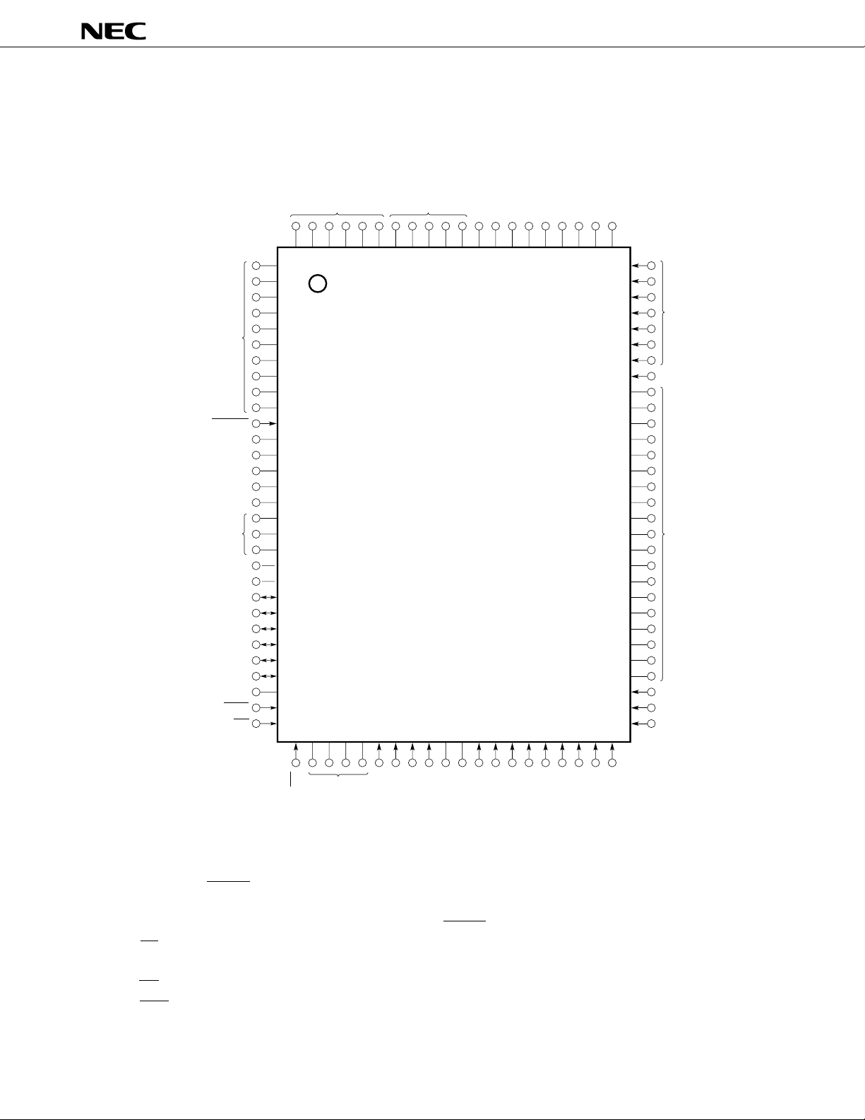
(2) PROM programming mode
• 100-pin plastic QFP (14 × 20 mm)
µ
PD78P4908GF-3BA
µ
PD78P4908
OPEN
RESET
OPEN
OPEN
V
PGM
OPEN
SS
V
(L)A9V
SS
OPEN
OPEN
VSSVSS
VDD
OPEN
81828384858687888990919293949596979899100
1
2
3
4
5
6
7
8
9
10
11
12
13
SS
V
VSS
14
15
V
16
SS
17
DD
18
19
D0
D1
D2
D3
D4
D5
D6
D7
(L)
20
21
22
23
24
25
26
27
28
29
CE
30
31 32 33 34 35 36 37 38 39 40 41 42 43 44 45 46 47 48 49 50
80
79
78
77
76
75
74
73
72
71
70
69
68
67
66
65
64
63
62
61
60
59
58
57
56
55
54
53
52
51
OPEN
PP
V
OPEN
A0
A1
A2
OE
(L)
A15
A14
A13
A12
SS
V
VDD
A11
A8A7A6A5A4
A10
A16
A3
Caution L : Connect these pins separately to the VSS pins through 10-kΩ pull-down resistors.
SS : To be connected to the ground.
V
Open : Nothing should be connected on these pins.
RESET: Set a low-level input.
A0-A16 : Address bus RESET : Reset
CE : Chip enable V
D0-D7 : Data bus V
OE : Output enable V
DD : Power supply
PP : Programming power supply
SS : Ground
PGM : Program
Data Sheet U11681EJ2V0DS00
9
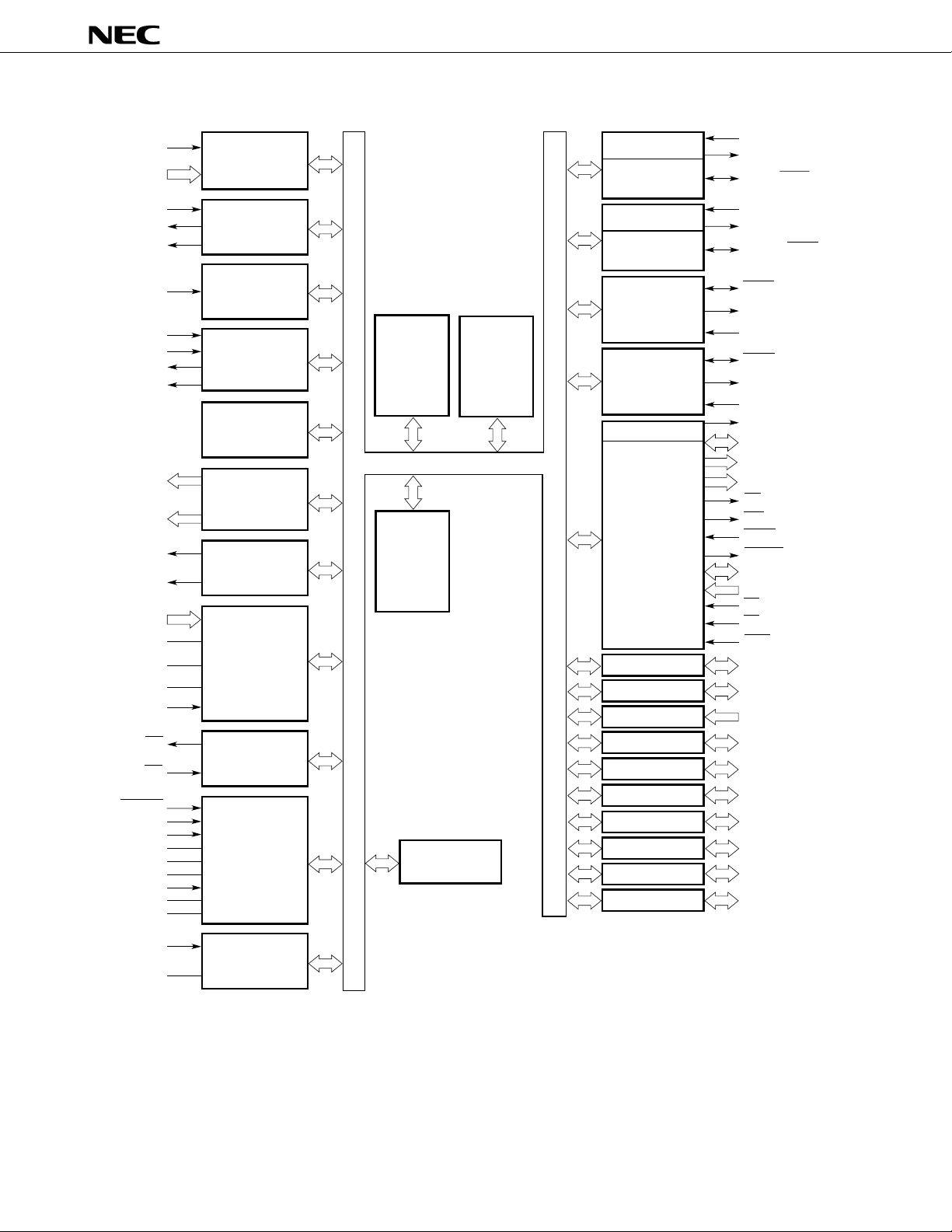
3. BLOCK DIAGRAM
µ
PD78P4908
NMI
INTP0-INTP5
INTP3
TO0
TO1
INTP0
INTP1
INTP2/CI
TO2
TO3
P00-P03
P04-P07
PWM0
PWM1
ANI0-ANI7
AVDD
AVREF1
AVSS
INTP5
TX
RX
RESET
TEST
X1
X2
REGC
REGOFF
Note
VPP
VDD
VSS
Programmable
interrupt controller
Timer/counter 0
(16 bits)
Timer/counter 1
(16 bits)
Timer/counter 2
(16 bits)
Timer 3
(16 bits)
Real-time output
port
PWM
A/D converter
IEBus controller
System control
(regulator)
78K/IV
CPU core
(RAM 512 bytes)
RAM
(3,840 bytes)
Watchdog timer
ROM
(128 Kbytes)
UART/IOE2
Baud-rate
generator
UART/IOE1
Baud-rate
generator
Clocked serial
interface
Clocked serial
interface 3
Clock output
Bus interface
Port 0
Port 1
Port 2
Port 3
Port 4
Port 5
Port 6
Port 7
Port 9
Port 10
RxD/SI1
TxD/SO1
ASCK/SCK1
RxD2/SI2
TxD2/SO2
ASCK2/SCK2
SCK0
SO0
SI0
SCK3
SO3
SI3
ASTB/CLKOUT
AD0-AD7
A8-A15
A16-A19
RD
WR
WAIT/HLDRQ
REFRQ/HLDAK
Note
D0-D7
Note
A0-A16
Note
CE
Note
OE
Note
PGM
P00-P07
P10-P17
P20-P27
P30-P37
P40-P47
P50-P57
P60-P67
P70-P77
P90-P97
P100-P107
XT1
Watch timer
XT2
Note In the PROM programming mode.
10
Data Sheet U11681EJ2V0DS00

4. PIN FUNCTIONS
4.1 PINS FOR NORMAL OPERATING MODE
(1) Port pins (1/2)
µ
PD78P4908
Pin
P00-P07
P10
P11
P12
P13
P14
P15-P17
P20
P21
P22
P23
P24
P25
P26
P27
P30
P31
P32
P33
P34-P37
P40-P47
I/O
I/O
Input
I/O
I/O
I/O
Also used as
—
—
—
ASCK2/SCK2
RxD2/SI2
TxD2/SO2
—
NMI
INTP0
INTP1
INTP2/CI
INTP3
INTP4/ASCK/SCK1
INTP5
SI0
RxD/SI1
TxD/SO1
SCK0
SO0
TO0-TO3
AD0-AD7
Function
Port 0 (P0):
• 8-bit I/O port.
• Functions as a real-time output port (4 bits × 2).
• Inputs and outputs can be specified bit by bit.
• The use of built-in pull-up resistors can be simultaneously specified by
software for all pins in input mode.
• Can drive a transistor.
Port 1 (P1):
• 8-bit I/O port.
• Inputs and outputs can be specified bit by bit.
• The use of built-in pull-up resistors can be simultaneously specified by
software for all pins in input mode.
• Can drive LED.
Port 2 (P2):
• 8-bit input-only port.
• P20 does not function as a general-purpose port (nonmaskable
interrupt). However, the input level can be checked by an interrupt
service routine.
• The use of built-in pull-up resistors can be specified by software for pins
P22 to P27 (in units of 6 bits).
• The P25/INTP4/ASCK/SCK1 pin functions as the SCK1 input/output pin
by CSIM1.
Port 3 (P3):
• 8-bit I/O port.
• Inputs and outputs can be specified bit by bit.
• The use of built-in pull-up resistors can be simultaneously specified by
software for all pins in input mode.
• P32 and P33 can be set as the N-ch open-drain pin.
Port 4 (P4):
• 8-bit I/O port.
• Inputs and outputs can be specified bit by bit.
• The use of built-in pull-up resistors can be simultaneously specified by
software for all pins in input mode.
• Can drive LED.
Data Sheet U11681EJ2V0DS00
11

(1) Port pins (2/2)
µ
PD78P4908
Pin
P50-P57
P60-P63
P64
P65
P66
P67
P70-P77
P90-P97
P100-P104
P105
P106
P107
I/O
I/O
I/O
I/O
I/O
I/O
Also used as
A8-A15
A16-A19
RD
WR
WAIT/HLDRQ
REFRQ/HLDAK
ANI0-ANI7
—
—
SCK3
SI3
SO3
Function
Port 5 (P5):
• 8-bit I/O port.
• Inputs and outputs can be specified bit by bit.
• The use of built-in pull-up resistors can be simultaneously specified by
software for all pins in input mode.
• Can drive LED.
Port 6 (P6):
• 8-bit I/O port.
• Inputs and outputs can be specified bit by bit.
• The use of built-in pull-up resistors can be simultaneously specified by
software for all pins in input mode.
Port 7 (P7):
• 8-bit I/O port.
• Inputs and outputs can be specified bit by bit.
Port 9 (P9):
• 8-bit I/O port.
• Inputs and outputs can be specified bit by bit.
• The use of built-in pull-up resistors can be simultaneously specified by
software for all pins in input mode.
Port 10 (P10):
• 8-bit I/O port.
• Inputs and outputs can be specified bit by bit.
• The use of built-in pull-up resistors can be simultaneously specified by
software for all pins in input mode.
• P105 and P107 can be set as the N-ch open-drain pin.
12
Data Sheet U11681EJ2V0DS00
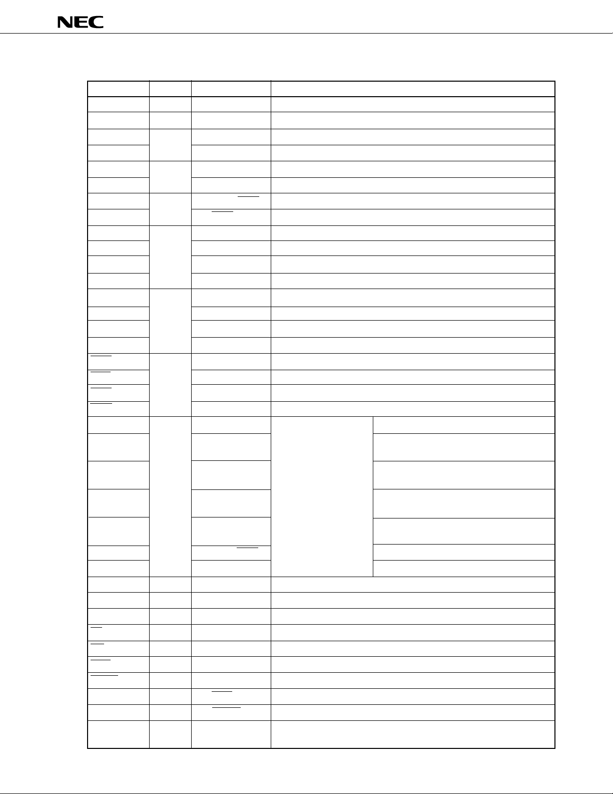
(2) Non-port pins (1/2)
µ
PD78P4908
Pin
TO0-TO3
CI
RxD
RxD2
TxD
TxD2
ASCK
ASCK2
SI0
SI1
SI2
SI3
SO0
SO1
SO2
SO3
SCK0
SCK1
SCK2
SCK3
NMI
INTP0
INTP1
INTP2
INTP3
INTP4
INTP5
AD0-AD7
A8-A15
A16-A19
RD
WR
WAIT
REFRQ
HLDRQ
HLDAK
ASTB
I/O
Output
Input
Input
Output
Input
Input
Output
I/O
Input
I/O
Output
Output
Output
Output
Input
Output
Input
Output
Output
Also used as
P34-P37
P23/INTP2
P30/SI1
P13/SI2
P31/SO1
P14/SO2
P25/INTP4/SCK1
P12/SCK2
P27
P30/RxD
P13/RxD2
P106
P33
P31/TxD
P14/TxD2
P107
P32
P25/INTP4/ASCK
P12/ASCK2
P105
P20
P21
P22
P23/CI
P24
P25/ASCK/SCK1
P26
P40-P47
P50-P57
P60-P63
P64
P65
P66/HLDRQ
P67/HLDAK
P66/WAIT
P67/REFRQ
CLKOUT
Function
Timer output
Input of a count clock for timer/counter 2
Serial data input (UART0)
Serial data input (UART2)
Serial data output (UART0)
Serial data output (UART2)
Baud rate clock input (UART0)
Baud rate clock input (UART2)
Serial data input (3-wire serial I/O 0)
Serial data input (3-wire serial I/O 1)
Serial data input (3-wire serial I/O 2)
Serial data input (3-wire serial I/O 3)
Serial data output (3-wire serial I/O 0)
Serial data output (3-wire serial I/O 1)
Serial data output (3-wire serial I/O 2)
Serial data output (3-wire serial I/O 3)
Serial clock I/O (3-wire serial I/O 0)
Serial clock I/O (3-wire serial I/O 1)
Serial clock I/O (3-wire serial I/O 2)
Serial clock I/O (3-wire serial I/O 3)
External interrupt request —
• Input of a count clock for timer/counter 1
• Capture/trigger signal for CR11 or CR12
• Input of a count clock for timer/counter 2
• Capture/trigger signal for CR22
• Input of a count clock for timer/counter 2
• Capture/trigger signal for CR21
• Input of a count clock for timer/counter 0
• Capture/trigger signal for CR02
—
Input of a conversion start trigger for A/D converter
Time multiplexing address/data bus (for connecting external memory)
High-order address bus (for connecting external memory)
High-order address during address expansion (for connecting external memory)
Strobe signal output for reading the contents of external memory
Strobe signal output for writing on external memory
Wait signal insertion
Refresh pulse output to external pseudo static memory
Input of bus hold request
Output of bus hold response
Latch timing output of time multiplexing address (A0-A7) (for connecting
external memory)
Data Sheet U11681EJ2V0DS00
13
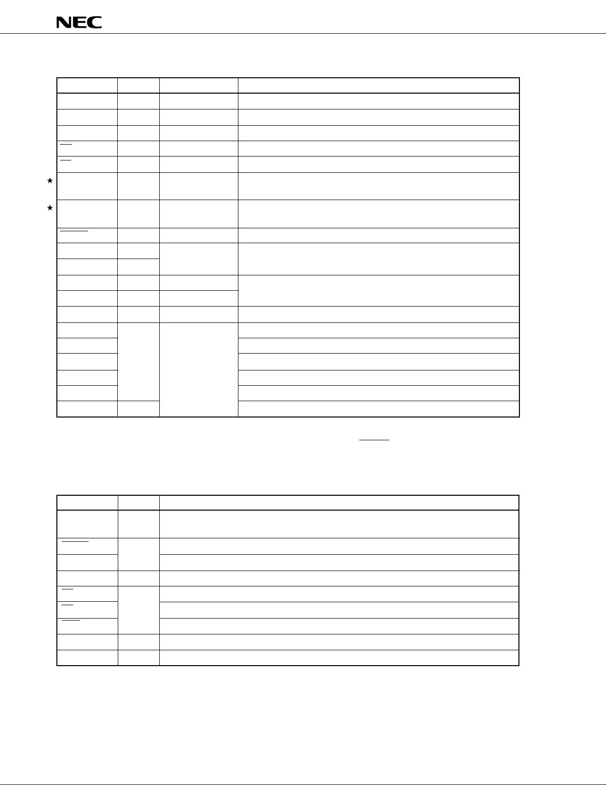
(2) Non-port pins (2/2)
µ
PD78P4908
Pin
CLKOUT
PWM0
PWM1
RX
TX
REGC
REGOFF
RESET
X1
X2
XT1
XT2
ANI0-ANI7
AV
REF1
AVDD
AVSS
VDD
VSS
TEST
I/O
Output
Output
Output
Input
Output
—
—
Input
Input
—
Input
—
Input
—
Input
Also used as
ASTB
P70-P77
—
—
—
—
—
—
—
—
—
—
—
Function
Clock output
PWM output 0
PWM output 1
Data input (IEBus)
Data output (IEBus)
Capacitor connection for stabilizing the regulator output/Power supply
when the regulator is stopped. Connect to V
Signal for specifying regulator operation. Directly connect to VSS (regulator
selected).
Chip reset
Crystal input for system clock oscillation (A clock pulse can also be input
to the X1 pin.)
Real-time clock connection
Analog voltage inputs for the A/D converter
Application of A/D converter reference voltage
Positive power supply for the A/D converter
Ground for the A/D converter
Positive power supply
Ground
Directly connect to V
SS. (The TEST pin is for the IC test.)
SS via a 1-
µ
F capacitor.
4.2 PINS FOR PROM PROGRAMMING MODE (VPP ≥ +5 V or +12.5 V, RESET = L)
4.2.1 Pin Functions
Pin name
V
PP
RESET
A0-A16
D0-D7
CE
OE
PGM
V
DD
VSS
Input
I/O
Input
I/O
—
—
—
PROM programming mode selection
High voltage input during program write or verification
PROM programming mode selection
Address bus
Data bus
PROM enable input/program pulse input
Read strobe input to PROM
Program/program inhibit input during PROM programming mode
Positive power supply
GND
Function
14
Data Sheet U11681EJ2V0DS00

4.2.2 Pin Functions
(1) V
PP (Programming power supply): Input
µ
Input pin for setting the
+6.5 V or more and when RESET input goes low, the
When CE is made low for V
PD78P4908 to the PROM programming mode. When the input voltage on this pin is
µ
PD78P4908 enters the PROM programming mode.
PP = +12.5 V and OE = high, program data on D0 to D7 can be written into the internal
PROM cell selected by A0 to A16.
(2) RESET (Reset): Input
µ
Input pin for setting the
the input voltage on the V
PD78P4908 to the PROM programming mode. When input on this pin is low, and when
PP pin goes +5 V or more, the
µ
PD78P4908 enters the PROM programming mode.
(3) A0 to A16 (Address bus): Input
Address bus that selects an internal PROM address (0000H to 1FFFFH)
(4) D0 to D7 (Data bus): I/O
Data bus through which a program is written on or read from internal PROM
µ
PD78P4908
(5) CE (Chip enable): Input
This pin inputs the enable signal from internal PROM. When this signal is active, a program can be written or
read.
(6) OE (Output enable): Input
This pin inputs the read strobe signal to internal PROM. When this signal is made active for CE = low, a onebyte program in the internal PROM cell selected by A0 to A16 can be read onto D0 to D7.
(7) PGM (Program): Input
The input pin for the operation mode control signal of the internal PROM.
Upon activation, writing to the internal PROM is enabled.
Upon inactivation, reading from the internal PROM is enabled.
DD
(8) V
Positive power supply pin
(9) V
SS
Ground potential pin
Data Sheet U11681EJ2V0DS00
15

4.3 I/O CIRCUITS FOR PINS AND HANDLING OF UNUSED PINS
Table 4-1 describes the types of I/O circuits for pins and the handling of unused pins.
Figure 4-1 shows the configuration of these various types of I/O circuits.
Table 4-1. Types of I/O Circuits for Pins and Handling of Unused Pins (1/2)
µ
PD78P4908
Pin
P00-P07
P10, P11
P12/ASCK2/SCK2
P13/RXD2/SI2
P14/TXD2/SO2
P15-P17
P20/NMI
P21/INTP0
P22/INTP1
P23/INTP2/CI
P24/INTP3
P25/INTP4/ASCK/SCK1
P26/INTP5
P27/SI0
P30/R
XD/SI1
P31/TXD/SO1
P32/SCK0
P33/SO0
P34/TO0-P37/TO3
P40/AD0-P47/AD7
P50/A8-P57/A15
P60/A16-P63/A19
P64/RD
P65/WR
P66/WAIT/HLDRQ
P67/REFRQ/HLDAK
P70/ANI0-P77/ANI7
P90-P97
P100-P104
P105/SCK3
P106/SI3
P107/SO3
ASTB/CLKOUT
I/O circuit type
5-A
8-A
5-A
2
2-A
8-A
2-A
5-A
10-A
5-A
20
5-A
10-A
8-A
10-A
4
I/O
I/O
Input
I/O
Input
I/O
I/O
Output
Recommended connection method for unused pins
Input state: To be connected to VDD
Output state: To be left open
To be connected to VDD or VSS
To be connected to VDD
Input state: To be connected to VDD
Output state: To be left open
To be connected to VDD
Input state: To be connected to VDD
Output state: To be left open
Input state: To be connected to V
Output state : To be left open
To be left open
DD or VSS
16
Data Sheet U11681EJ2V0DS00

µ
PD78P4908
Table 4-1. Types of I/O Circuits for Pins and Handling of Unused Pins (2/2)
Pin
RESET
TEST
XT2
XT1
PWM0, PWM1
RX
TX
AV
REF1
AVSS
AVDD
I/O circuit type
2
1
—
3
1
3
—
I/O
Input
—
Input
Output
Input
Output
—
Caution When the I/O mode of an I/O dual-function pin is unpredictable, connect the pin to V
Recommended connection method for unused pins
—
To be connected to V
To be left open
To be connected to VSS
To be left open
To be connected to VDD or VSS
To be left open
To be connected to VSS
To be connected to VDD
SS directly
DD through
a resistor of 10 to 100 kΩ (particularly when the voltage of the reset input pin becomes higher
than that of the low level input at power-on or when I/O is switched by software).
Remark Since type numbers are consistent in the 78K series, those numbers are not always serial in each product.
(Some circuits are not included.)
Data Sheet U11681EJ2V0DS00
17
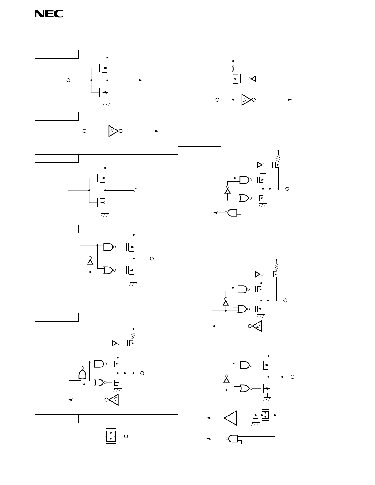
Figure 4-1. I/O Circuits for Pins
Data
V
DD
P
N
IN/OUT
Output
disable
VDD
P
Pull-up
enable
Input
enable
Data
V
DD
P
N
IN/OUT
Output
disable
VDD
P
Pull-up
enable
µ
PD78P4908
Type 1
VDD
P
IN
N
Type 2
IN
Schmitt trigger input with hysteresis characteristics
Type 3
V
DD
P-ch
Data OUT
N-ch
Type 4
VDD
Data
P
Type 2-A
VDD
P
Pull-up
enable
IN
Schmitt trigger input with hysteresis characteristics
Type 5-A
Type 8-A
Output
disable
Push-pull output which can output high impedance
(both the positive and negative channels are off.)
Type 10-A
Pull-up
enable
Data
P
Open
drain
Output
N
disable
Type 12
Analog output
voltage
P
N
18
OUT
N
VDD
P
Type 20
V
V
DD
Data
IN/OUT
Output
disable
DD
P
IN/OUT
N
Comparator
P
N
OUT
+
–
(Threshold voltage)
VREF
Input
enable
Data Sheet U11681EJ2V0DS00
µ
PD78P4908
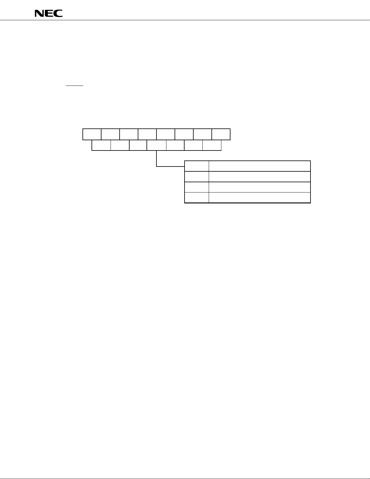
5. INTERNAL MEMORY SIZE SELECT REGISTER (IMS)
This register enables the software to avoid using part of the internal memory. The IMS can be set to establish
the same memory mapping as used in mask ROM products that have different internal memory (ROM and RAM)
configurations.
The IMS is set using 8-bit memory operation instructions.
A RESET input sets the IMS to FFH.
Figure 5-1. Internal Memory Size Select Register (IMS)
76543210
IMS IMS7 IMS6
The IMS is not contained in a mask ROM product (
IMS5
IMS4 IMS3 IMS2 IMS1 IMS0
IMS0-7
FFH
EEH
Other than
the above
µ
PD784907 or µPD784908). But the action is not affected if
Same as the PD784908
Same as the PD784907
Not to be set
the write command to the IMS is executed to the mask ROM product.
Address
0FFFCH
Memory size
µ
µ
Reset valueWR/W
FFH
Data Sheet U11681EJ2V0DS00
19

µ
PD78P4908
6. PROM PROGRAMMING
The µPD78P4908 has an on-chip 128-KB PROM device for use as program memory. When programming, set
PP and RESET pins for PROM programming mode. See 2. PIN CONFIGURATION (TOP VIEW) (2) PROM
the V
programming mode with regard to handling of other, unused pins.
6.1 OPERATION MODE
PROM programming mode is selected when +6.5 V is added to the V
low-level input is added to the RESET pin. This mode can be set to operation mode by setting the CE pin, OE pin,
and PGM pin as shown in Table 6-1 below.
In addition, the PROM contents can be read by setting read mode.
Table 6-1. PROM Programming Operation Mode
Pin RESET VPP VDD CE OE PGM D0-D7
Operation mode
Page data latch L +12.5 V +6.5 V H L H Data input
Page write H H L High impedance
DD pin, +12.5 V is added to the VPP pin, or
Byte write L H L Data input
Program verify L L H Data output
Program inhibit × H H High impedance
× LL
Read +5 V +5 V L L H Data output
Output disable L H × High impedance
Standby H ×× High impedance
Remark × = L or H
20
Data Sheet U11681EJ2V0DS00
 Loading...