
DATA SHEET
MOS INTEGRATED CIRCUIT
m
PD78P368A
16/8 BIT SINGLE-CHIP MICROCOMPUTER
The mPD78P368A is produced by replacing the internal mask ROM of the mPD78366A with a one-time PROM
or EPROM. One-time PROM products, in which data can be written once are effective for manufacture of small
quantities of multiple products and early stage start-up of application. EPROM products, to which programs can
be re-written after previously written programs have been erased, are suited for system evaluation.
The following user's manual describes the details of functions. Be sure to read it before design.
m
PD78366A User's Manual, Hardware: U10205E
m
PD78356 User's Manual, Instructions: IEU-1395
FEATURES
• Compatible with the
• Can be replaced with the
• Internal PROM: 48K bytes
• Data can be written once (one-time PROM product without an erasure window)
• Written data can be erased by exposure to ultraviolet light and re-written electrically (EPROM product with an
erasure window)
• PROM programming characteristics: Compatible with the
• QTOP
ORDERING INFORMATION
TM
microcomputer
Remark The QTOP microcomputer is a single-chip microcomputer with a built-in one-time PROM that is totally
supported by NEC. The support includes writing application programs, marking, screening, and
verification.
Part number Package Internal ROM
m
PD78P368AGF-3B9 80-pin plastic QFP (14 ¥ 20 mm) One-time PROM
m
PD78P368AKL-S
Note Under development
m
PD78366A
Note
m
PD78366A containing mask ROM on a full-production basis.
m
PD27C1001A
80-pin ceramic WQFN EPROM
In this manual, the description of the PROM is for both a one-time PROM and EPROM.
(Previous No. IP-3680)
Date Published June 1996 P
Printed in Japan
The information in this document is subject to change without notice.
The mark H shows major revised points.Document No. U11373EJ1V0DS00 (1st edition)
1996
©
1990
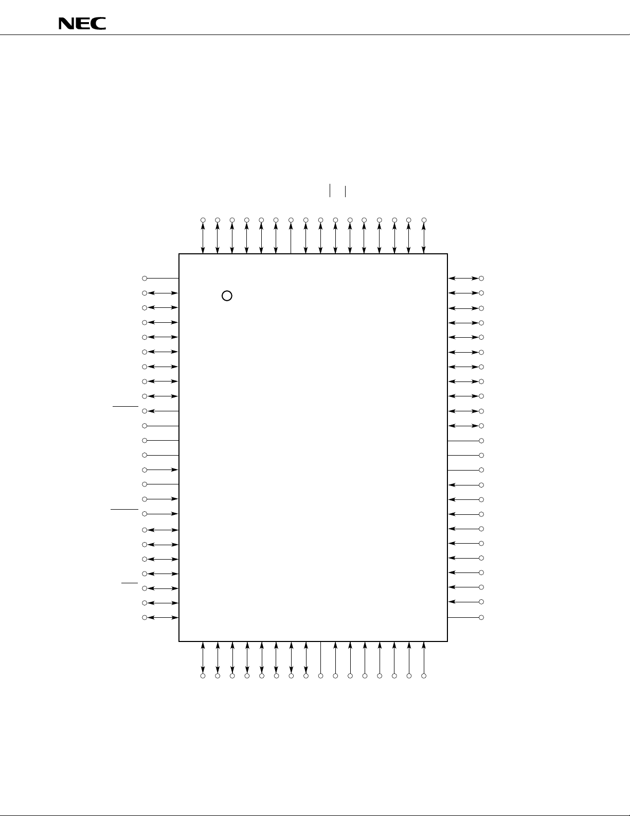
PIN CONFIGURATION (TOP VIEW)
(1) Normal operation mode (MODE0 = L, MODE1 = L)
• 80-pin plastic QFP (14 ¥ 20 mm)
m
PD78P368AGF-3B9
• 80-pin ceramic WQFN
m
PD78P368AKL-S
m
PD78P368A
V
P00/RTP0
P01/RTP1
P02/RTP2
P03/RTP3
P04/PWM0
P05/ TCUD/PWM1
P06/ TIUD/TO40
P07/ TCLRUD
WDTO
IC
V
V
X1
X2
MODE1
RESET
X
D0
P30/ T
P31/RXD0
P32/SO/SB0
P33/SI/SBI
P34/SCK
X
D1
P35/ T
X
D1
P36/R
P84/ TO04
P83/ TO03
P82/TO02
P81/ TO01
P80/ TO00
ASTB
P93
P92
P91/ WR
P90/RD
P57/A15
P56/A14
P55/A13
P54/A12
P53/A11
P85/ TO05
80 79 78 77 76 75 74 73 72 71 70 69 68 67 66 65
SS
DD
SS
1
2
3
4
5
6
7
8
9
10
11
12
13
14
15
16
17
18
19
20
21
22
23
24
64
63
62
61
60
59
58
57
56
55
54
53
52
51
50
49
48
47
46
45
44
43
42
41
P52/A10
P51/A9
P50/A8
P47/AD7
P46/AD6
P45/AD5
P44/AD4
P43/AD3
P42/AD2
P41/AD1
P40/AD0
SS
V
V
DD
AV
DD
AV
REF
P77/ANI7
P76/ANI6
P75/ANI5
P74/ANI4
P73/ANI3
P72/ANI2
P71/ANI1
P70/ANI0
SS
AV
25 26 27 28 29 30 31 32 33 34 35 36 37 38 39 40
P10
P11
P12
Caution Directly connect the IC pin to V
Remark Pin compatible with the mPD78366AGF
2
P13
SS.
P14
P15
P16
P17
SS
V
MODE0
P20/NMI
P21/INTP0
P22/INTP1
P23/INTP2
P25/INTP4
P24/INTP3/ TI

m
PD78P368A
P00-P07: Port 0
P10-P17: Port 1
P20-P25: Port 2
P30-P36: Port 3
P40-P47: Port 4
P50-P57: Port 5
P70-P77: Port 7
P80-P85: Port 8
P90-P93: Port 9
RTP0-RTP3: Real-time port
NMI: Nonmaskable interrupt
INTP0-INTP4: Interrupt from peripherals
TO00-TO05, TO40: Timer output
TI: Timer input
TIUD: Timer input for up/down
counter
TCUD: Timer control for up/down
counter
TCLRUD: Timer clear for up/down
counter
ANI0-ANI7: Analog input
TxD0, TxD1: Transmit data
RxD0, RxD1: Receive data
SI: Serial input
SO: Serial output
SB0, SB1: Serial bus
SCK: Serial clock
PWM0, PWM1: Pulse width modulation output
WDTO: Watchdog timer output
MODE0, MODE1: Mode
AD0-AD7: Address/data bus
A8-A15: Address bus
ASTB: Address strobe
RD: Read strobe
WR: Write strobe
RESET: Reset
X1, X2: Crystal
DD: Analog VDD
AV
AVSS: Analog VSS
AVREF: Analog reference voltage
DD: Power supply
V
SS: Ground
V
IC: Internally connected
3
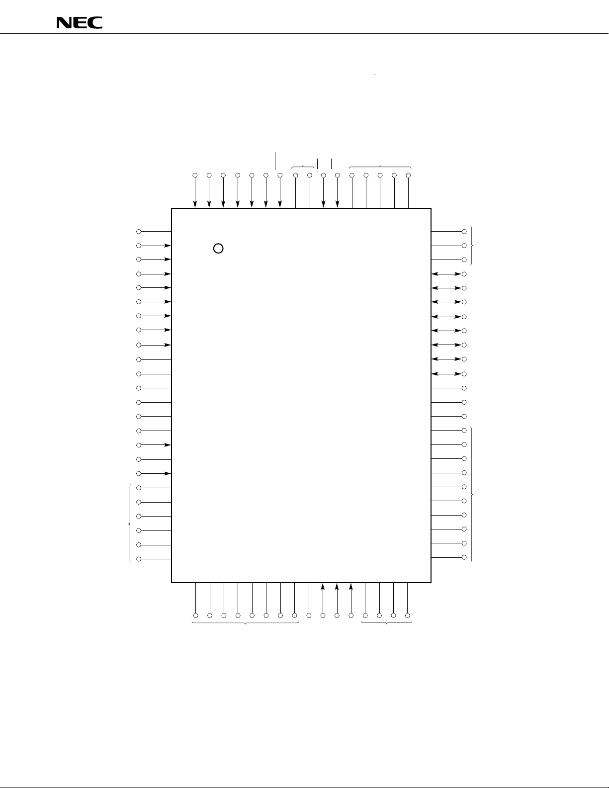
(2) PROM programming mode (MODE0/VPP = H, MODE1 = L)
• 80-pin plastic QFP (14 ¥ 20 mm)
m
PD78P368AGF-3B9
• 80-pin ceramic WQFN
m
PD78P368AKL-S
m
PD78P368A
VSS
A0
A1
A2
A3
A4
A5
A6
A7
(Open)
(G)
VDD
VSS
(G)
(Open)
MODE1
(G)
A16
(L)
(L)
A15
A14
A13
A11
A10
A12
80 79 78 77 76 75 74 73 72 71 70 69 68 67 66 65
1
2
3
4
5
6
7
8
9
10
11
12
13
14
15
16
17
18
19
20
21
22
23
24
25 26 27 28 29 30 31 32 33 34 35 36 37 38 39 40
PGM
CE
OE
(L)
64
63
62
61
60
59
58
57
56
55
54
53
52
51
50
49
48
47
46
45
44
43
42
41
D7
D6
D5
D4
D3
D2
D1
D0
V
VDD
VDD
(L)
SS
(G)
A9
VSS
(L)
A8
(G)
MODE0/ VPP
Caution Symbols in parentheses denote how the pins not used in the PROM programming mode should
be treated.
L: Connect these pins to the V
G: Connect these pins to the V
SS pins through separate resistors.
SS pins.
Open: Do not connect these pins to anything.
4

m
PD78P368A
A0-A16: Address bus
D0-D7: Data bus
CE: Chip enable
OE: Output enable
PGM: Programming mode
MODE0, MODE1: Programming mode set
PP: Programming power supply
V
DD: Power supply
V
SS: Ground
V
5
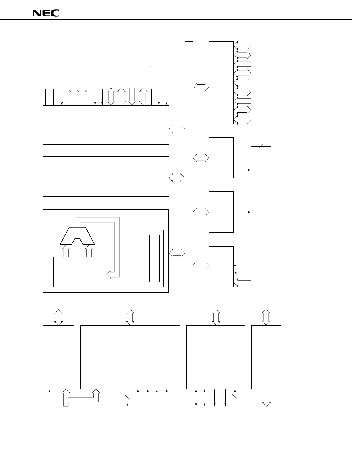
BLOCK DIAGRAM
X1X2RESET
BCU
ASTBRDWR
MODE1
System
control
Note
PP
MODE0/V
&
Bus
A8-A15
8
control
&
A0-A16
AD0-AD7
8
17
Prefetch
control
Note
D0-D7
8
PGM
CE
OE
Port
Watchdog
timer
m
PD78P368A
P0
8
8
P1
6
P2
7
P3
8
P4
P5
8
8
P7
6
P8
4
P9
2
DD
V
4
V
SS
WDTO
PROM/RAM
EXU
Main RAM
128 × 8
General
registers
ALU
&
PROM
Data
memory
Periph-
&
eral RAM
1792 × 8
Micro
sequence
control
Micro ROM
PWM
A/D
converter
2
PWM
DD
AV
AV
SS
AV
REF
INTP2
8
ANI
48K × 8
128 × 8
Note Shading indicates the pins used in the PROM programming mode.
(SBI)
(UART)
Serial
interface
Programmable
interrupt
NMI
controller
5
5
INTP
(Real-time pulse unit)
Timer/counter unit
4
7
TI
TO
TIUD
TCUD
TCLRUD
SCK
SO/SB0
2
SI/SB1
TxD
2
RxD
Real-time output
port
4
RTP
6

m
PD78P368A
CONTENTS
1. PIN FUNCTIONS........................................................................................................................ 8
1.1 NORMAL OPERATION MODE (MODE0 = L, MODE1 = L) ......................................................... 8
1.2 PROM PROGRAMMING MODE (MODE0/V
1.3 INPUT/OUTPUT CIRCUIT TYPE FOR EACH PIN AND HANDLING OF UNUSED PINS .......... 1 1
PP = H, MODE1 = L) ................................................ 10
2. MEMORY CONFIGURATION................................................................................................... 13
3. DIFFERENCES BETWEEN THE mPD78P368A AND mPD78366A ......................................... 1 4
4. PROM PROGRAMMING ............................................................................................................ 15
4.1 OPERATION MODE........................................................................................................................ 15
4.2 PROCEDURE FOR WRITING ON PROM (PAGE PROGRAM MODE)............................... 16
4.3 PROCEDURE FOR WRITING ON PROM (BYTE PROGRAM MODE) ................................ 18
4.4 PROCEDURE FOR READING FROM PROM ........................................................................... 21
5. ERASURE CHARACTERISTICS (mPD78P368AKL-S ONLY) ................................................ 22
6. PROTECTIVE FILM COVERING THE ERASURE WINDOW (mPD78P368AKL-S ONLY)........ 22
7. SCREENING ONE-TIME PROM PRODUCTS.......................................................................... 22
8. ELECTRICAL SPECIFICATIONS ............................................................................................. 23
9. PACKAGE DRAWINGS ............................................................................................................. 39
10. RECOMMENDED SOLDERING CONDITIONS...................................................................... 41
APPENDIX A TOOLS...................................................................................................................... 42
A.1 DEVELOPMENT TOOLS ................................................................................................................ 42
A.2 EMBEDDED SOFTWARE............................................................................................................... 47
APPENDIX B DIMENSIONS OF THE CONVERSION SOCKET AND RECOMMENDED
PATTERN ON BOARDS ......................................................................................... 49
H
H
7

1. PIN FUNCTIONS
1.1 NORMAL OPERATION MODE (MODE0 = L, MODE1 = L)
(1) Port pins
m
PD78P368A
P00-P03
P04
P05
P06
P07
P10-P17
P20
P21
P22
P23
P24
P25
P30
P31
P32
P33
P34
P35
P36
P40-P47
P50-P57
P70-P77
I/O Dual-function pinPin name
I/O
I/O
I/O
I/O
I/O
Function
Port 0.
8-bit I/O port.
Can be specified as input or output bit by bit.
Port 1.
8-bit I/O port.
Can be specified as input or output bit by bit.
I
I
Port 2.
Port used only for 6-bit input.
Port 3.
7-bit I/O port.
Can be specified as input or output bit by bit.
Port 4.
8-bit I/O port.
Can be specified as input or output in units of 8 bits.
Port 5.
8-bit I/O port.
Can be specified as input or output bit by bit.
Port 7.
Port used only for 8-bit input.
RTP0-RTP3
PWM0
TCUD/PWM1
TIUD/TO40
TCLRUD
–
NMI
INTP0
INTP1
INTP2
INTP3/TI
INTP4
TxD0
RxD0
SO/SB0
SI/SB1
SCK
TxD1
RxD1
AD0-AD7
A8-A15
ANI0-ANI7
8
P80-P85
P90
P91
P92
P93
I/O
I/O
Port 8.
6-bit I/O port.
Can be specified as input or output bit by bit.
Port 9.
4-bit I/O port.
Can be specified as input or output bit by bit.
TO00 - TO05
RD
WR
–
–

(2) Non-port pins (1/2)
m
PD78P368A
RTP0-RTP3
NMI
INTP0
INTP1
INTP2
INTP3
INTP4
TI
TCUD
TIUD
TCLRUD
TO00-TO05
TO40
ANI0-ANI7
TxD0
TxD1
RxD0
RxD1
SCK
SI
SO
SB0
SB1
PWM0
PWM1
WDTO
AD0-AD7
A8-A15
ASTB
RD
WR
I/O
I/O
I/O
I/O
Function
O
I
I
O
I
O
I
I
O
O
O
O
Outputs a pulse in real time as triggered by a trigger signal sent from the
real-time pulse unit.
Nonmaskable interrupt request input
External interrupt request input
External count clock input to timer 1
Input for the control signal to determine whether the up/down counter (timer
4) counts up or down.
External count clock input to the up/down counter (timer 4)
Clear signal input to the up/down counter (timer 4)
Pulse output from the real-time pulse unit
Analog input to the A/D converter
Serial data output from the asynchronous serial interface
Serial data input to the asynchronous serial interface
Serial clock I/O for the clock synchronous serial interface
Serial data input to the clock synchronous serial interface in the 3-wire mode
Serial data output from the clock synchronous serial interface in the 3-wire
mode
Serial data I/O for the clock synchronous serial interface in the SBI mode
PWM signal output
Output for the signal which indicates the watchdog timer overflowed. (A
nonmaskable interrupt is generated.)
Multiplexed address/data bus used when external memory is expanded
Address bus used when external memory is expanded
Output for the timing signal used in externally latching address information
output from the AD0 to AD7 and A8 to A15 pins, in order to access the
external memory
Read strobe signal output to the external memory
Write strobe signal output to the external memory
Dual-function pinPin name
P00-P03
P20
P21
P22
P23
P24/TI
P25
P24/INTP3
P05/PWM1
P06/TO40
P07
P80-P85
P06/TIUD
P70-P77
P30
P35
P31
P36
P34
P33/SB1
P32/SB0
P32/SO
P33/SI
P04
P05/TCUD
–
P40-P47
P50-P57
–
P90
P91
9

(2) Non-port pins (2/2)
m
PD78P368A
I/O Dual-function pinPin name
MODE0
MODE1
RESET
X1
X2
AVREF
AVDD
AVSS
VDD
VSS
IC
I
I
I
–
I
–
–
–
–
–
Input for the control signal which sets the operation mode. Normally, both
MODE0 and MODE1 are directly connected to the VSS pin.
System reset input
Crystal input pin for the system clock. A clock signal provided externally is
input to the X1 pin. The reversed signal of the clock signal is input to the
X2 pin.
A/D converter reference voltage input
Analog power supply for the A/D converter
Ground for the A/D converter
Positive power supply
Ground
Internally connected. Directly connect the IC pin to VSS.
1.2 PROM PROGRAMMING MODE (MODE0/V
Pin name
MODE0/VPP
MODE1
A0-A16
D0-D7
PGM
CE
OE
VDD
VSS
I/O
PROM programming mode set/programming supply voltage
I
PROM programming mode set
I
Address bus
I
Data bus
I/O
Program input
I
Enable PROM
I
Read strobe to PROM
I
Positive power supply
GND
Function
–
–
–
–
–
–
–
–
–
PP = H, MODE1 = L)
Function
10

m
PD78P368A
1.3 INPUT/OUTPUT CIRCUIT TYPE FOR EACH PIN AND HANDLING OF UNUSED PINS
Table 1-1 lists the input and output circuit type for each pin and how to handle it when it is not used. Fig. 1-1 shows
the circuits.
Table 1-1 Input/Output Circuit Type for Each Pin and Recommended Connection Methods for Unused
Pins
P00/RTP0-P03/RTP3
P04/PWM0
P05/TCUD/PWM1
P06/TIUD/TO40
P07/TCLRUD
P10-P17
P20/NMI
P21/INTP0
P22/INTP1
P23/INTP2
P24/INTP3/TI
P25/INTP4
P30/TxD0
P31/RxD0
P32/SO/SB0
P33/SI/SB1
P34/SCK
P35/TxD1
P36/RxD1
P40/AD0-P47/AD7
P50/A8-P57/A15
P70/ANI0-P77/ANI7
P80/TO00-P85/TO05
P90/RD
P91/WR
P92, P93
ASTB
WDTO
MODE0, MODE1
RESET
AVREF, AVSS
AVDD
Pin
I/O circuit type
5-A
2
2-A
5-A
8-A
5-A
9
5-A
5
19
1
2
–
Recommended connection method
Input state: Each pin is connected to the V DD or
VSS pin via a separate resistor.
Output state: Open
Connected to the VSS pin.
Input state: Each pin is connected to the V DD or
VSS pin via a separate resistor.
Output state: Open
Connected to the VSS pin.
Input state: Each pin is connected to the V DD or
VSS pin via a separate resistor.
Output state: Open
Connected to the VSS pin.
–
Connected to the VSS pin.
Connected to the VDD pin.
11
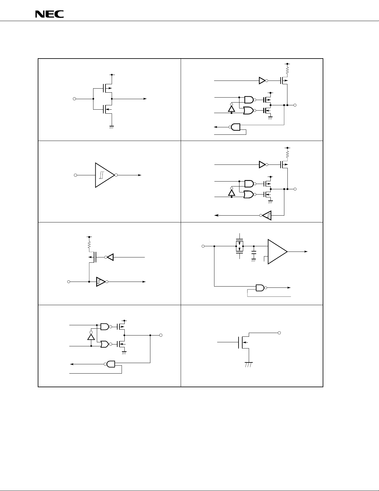
Fig. 1-1 Input/Output Circuits of Each Pin
Input
enable
Output
disable
Pull-up
enable
Data
IN/OUT
N-ch
V
DD
P-ch
V
DD
P-ch
N-ch
OUT
m
PD78P368A
Type 1 Type 5-A
DD
V
P-ch
IN
N-ch
Type 2 Type 8-A
Pull-up
IN
enable
Data
Output
disable
Schmitt trigger input with hysteresis characteristics
Type 2-A Type 9
V
DD
IN
P-ch
Pull-up
enable
IN
Schmitt trigger input with hysterisis characteristics
P-ch
N-ch
V
DD
P-ch
N-ch
Comparator
+
–
V
ref
(Threshold voltage)
V
DD
P-ch
Input
enable
IN/OUT
Type 5 Type 19
Data
Output
disable
V
DD
P-ch
IN/OUT
N-ch
Input
enable
12
2. MEMORY CONFIGURATION
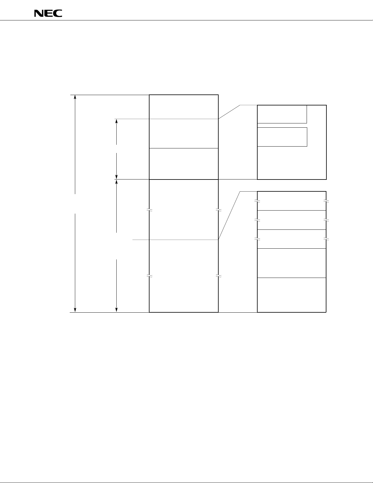
The mPD78P368A can access memory of up to 64K bytes. Fig. 2-1 shows the memory map.
Fig. 2-1 Memory Map
MODE 0, 1 = LL
Data memory
FFFFH
FF00H
FEFFH
FE00H
FDFFH
F700H
F6FFH
Special function
register (SFR)
(256 × 8)
Main RAM
(256 × 8)
Peripheral RAM
(1792 × 8)
FEFFH
FE80H
FE25H
FE06H
F700H
General register
(128 × 8)
Macro service control
(32 × 8)
m
PD78P368A
Data area
(2048 × 8)
Memory
space
(64K × 8)
Program
memory
Data
memory
C000H
BFFFH
0000H
External memory
(14080 × 8)
Internal PROM
(49152 × 8)
Note
BFFFH
1000H
0FFFH
0800H
07FFH
0080H
007FH
0040H
003FH
0000H
Program area
CALLF instruction
entry area
(2048 × 8)
Program area
CALLT instruction
table area
(64 × 8)
Vector table area
(64 × 8)
Note Access in the external memory expansion mode.
Caution When word access (including the stack operation) to the main RAM space (FE00H to FEFFH) is
executed, the addresses specified in the operand must be even numbers.
13

m
PD78P368A
3. DIFFERENCES BETWEEN THE
mm
m
PD78P368A AND
mm
mm
m
PD78366A
mm
The mPD78P368A is produced by replacing the internal mask ROM of the mPD78366A with a 48K-byte PROM.
Both have the same functions except some differences in ROM specifications, such as write and verify modes. Table
3-1 shows the differences.
m
In this manual, the functions specific to the
m
to the
PD78366A document.
Table 3-1 Differences between the
Item
ROM
Internal program memory
(Electrical write)
PROM programming pin
Setting of MODE0 and
MODE1
Package
Electrical characteristics
Others
Part number
48K bytes
One-time PROM
(Data can be written once)
Provided
• Normal operation mode
MODE0, 1 = LL
• PROM programming mode
MODE0, 1 = HL
80-pin plastic QFP
They differ in supply current and other factors.
Since each product has a different circuit scale and mask layout, the noise immunity and
noise radiation of each product differ.
PD78P368A are explained. For details of the other functions, refer
mm
m
PD78P368A and mPD78366A
mm
m
m
PD78P368A
EPROM (Data can be
written multiple times)
80-pin ceramic WQFN
32K bytes
Mask ROM
Not provided
• Normal operation mode
• ROM-less mode
80-pin plastic QFP
PD78366A
MODE0, 1 = LL
MODE0, 1 = HH
Cautions1. The PROM and mask ROM products differ in noise immunity and noise radiation. Use not ES
products but CS products (mask ROM products) to evaluate them thoroughly when considering
the change from the PROM products to the mask ROM products during processes from
preproduction to volume production.
2. Connect the MODE0 and MODE1 pins directly to the V
DD or VSS pin.
14
m
PD78P368A
4. PROM PROGRAMMING
The mPD78P368A is provided with an electrically writable PROM of 48K ¥ 8 bits. When programming this PROM,
use the MODE0/V
The
m
PD78P368A provides programming characteristics compatibility with the mPD27C1001A.
PP and MODE1 pins to set the
Table 4-1 Pin Functions in Programming Mode
m
PD78P368A to the PROM programming mode.
Function
Address input
Data input
Program pulse
Chip enable
Output enable
Program voltage
Mode control
Normal operation mode
P00-P07, P21, P20, P80-P85, P30
P40-P47
ASTB
P91
P90
MODE0/VPP
MODE1
Programming mode
A0-A16
D0-D7
PGM
CE
OE
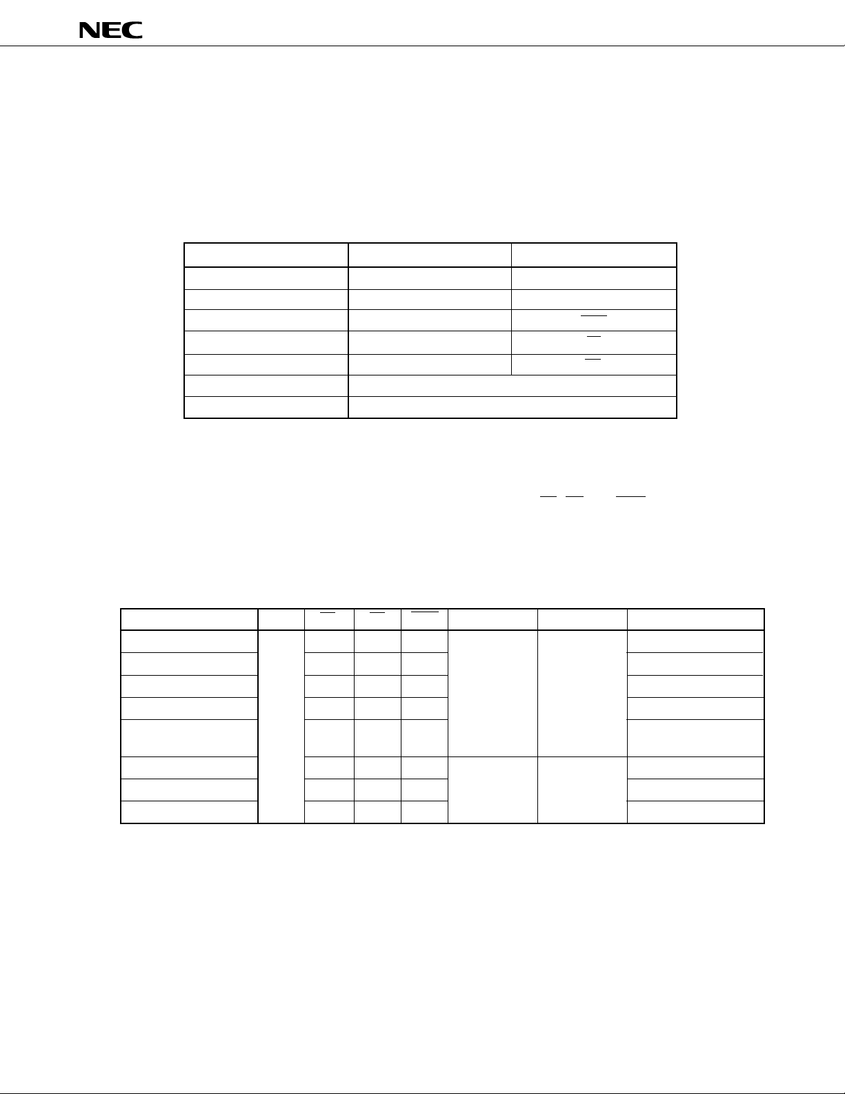
4.1 OPERATION MODE
To enter the program write/verify mode, set each pin as follows: MODE0/V
PP = H, MODE1 = L. In addition, any
of the operation modes listed in Table 4-2 can be selected by setting the CE, OE, and PGM pins in this mode.
m
Set the
PD78P368A to the read mode in order to read the contents of PROM.
Handle unused pins as described in PIN CONFIGURATION (2).
Table 4-2 Operation Modes for PROM Programming
Mode
Page data latch
Page program
Byte program
Program verify
Program inhibit
Read
Output disable
Standby
MODE1
L
CE
H
H
L
L
¥
¥
L
L
H
OE
L
H
H
L
L
H
L
H
¥
PGM
H
L
L
H
L
H
H
¥
¥
MODE0/VPP
+12.5 V
+5 V
VDD
+6.5 V
+5 V
D0-D7
Data input
High impedance
Data input
Data output
High impedance
Data output
High impedance
High impedance
Remark ¥: L or H
15

m
PD78P368A
4.2 PROCEDURE FOR WRITING ON PROM (PAGE PROGRAM MODE)
The following is a procedure for writing on PROM. (See Fig. 4-1.)
In the page program mode, data is written in units of pages (four bytes). When write data completes midway of
a page, latch FFH after the data so that the data fits into pages.
(1) Always set each pin as follows: MODE0/V
CONFIGURATION (2).
(2) Apply +6.5 V to the VDD pin and +12.5 V to the VPP pin.
(3) Input an initial address to the A0 to A16 pins.
(4) Clear the page counter.
(5) Data latch mode. Input write data to the D0 to D7 pins and input an active-low pulse to the OE pin. Increment
the address and the page counter.
(6) Repeat step (5) for a page (four bytes).
(7) Input a 0.1 ms program pulse (active low) to the PGM pin.
(8) Verify mode. Checks if data has been written in PROM.
Apply a low level to the CE pin, input an active-low pulse to the OE pin, and then read the write data from the
D0 to D7 pins. Repeat this for a page (four bytes). When verification completes, apply a high level to the CE
pin.
• If data has been written, go to step (10).
• If not, repeat steps (7) and (8). If no data is written yet after the steps have been repeated 10 times, go to
step (9).
(9) Assume the device to be defective and stop write operation.
(10) Increment the address.
(11) Repeat steps (4) to (10) until the address exceeds the last address.
Fig. 4-2 is a timing chart of these steps (2) to (9).
PP = H and MODE1 = L. Connect unused pins according to PIN
16
 Loading...