
4-BIT SINGLE-CHIP MICROCOMPUTER
DESCRIPTION
The µPD75208 is a microcomputer with a CPU capable of 1-, 4-, and 8-bit-wise data processing, a ROM, a RAM,
I/O ports, a fluorescent display tube controller/driver, a watch timer, a timer/pulse generator capable of outputting
14-bit PWM, a serial interface and a vectored interrupt function integrated on a single-chip.
It uses the VCR, ECR and CD fluorescent display tubes as display devices and is most suitable for applications
requiring the timer/watch function and high-speed interrupt servicing. It can help to provide the unit with many
functions and to decrease performance costs.
With the
µ
PD75208, the µPD75P216A, 75P218 one-time PROM products are available for system development
evaluation or small production.
The following manual provides detailed description of the functions of the
µ
PD75208. Be sure to read this manual
when you design an application system.
µ
PD75216A User’s Manual: IEM-988
FEATURES
µ
PD75208
MOS INTEGRATED CIRCUIT
DATA SHEET
The information in this document is subject to change without notice.
The mark ★ shows major revised points.
Document No. IC-1884A
(O. D. No. IC-7048C)
Date Published August 1993 P
Printed in Japan
Please refer to “Quality grade on NEC Semiconductor Devices” (Document number IEI-1209) published by
NEC Corporation to know the specification of quality grade on the devices and its recommended applications.
• Architecture equal to that of an 8-bit microcomputer
• High-speed operation : Minimum instruction execution time : 0.95
µ
s (when operated at 4.19 MHz)
• Instruction execution time variable function realizing a wide range of operating voltages
• On-chip large-capacity program memory : 8K bytes
• Watch operation with an ultra low current consumption : 5
µ
A TYP. (at the 3 V operation)
• On-chip programmable fluorescent display tube controller/driver
• Timer function : 4 ch
• 14-bit PWM output capability with the voltage synthesizer type electronic tuner
• Buzzer output capability
• Interrupt function with importance attached to applications
• For power-off detection
• For remote controlled reception
• Product with an on-chip PROM :
µ
PD75P216A, µPD75P218 (on-chip EPROM : WQFN package)
ORDERING INFORMATION
Ordering Code Package Quality Grade
µ
PD75208CW-××× 64-pin plastic shrink DIP (750 mil) Standard
µ
PD75208GF-×××-3BE 64-pin plastic QFP (14 × 20 mm) Standard
© NEC Corporation 1991
★
★
★

2
µ
PD75208
Instruction execution time
On-chip memory ROM
RAM
General register
Input/output port
FIP dual-function pin
included
FIP dedicated pin
excluded
FIP controller/driver
Timer
Serial interface
Vectored interrupt
Test input
System clock oscillator
Standby function
Mask option
Operating temperature range
Operating voltage
Package
• 0.95, 1.91, 15.3 µs (Main system clock : 4.19 MHz operation)
• 122 µs (Subsystem clock : 32.768 kHz operation)
8064 × 8 bits
497 × 4 bits
• 4-bit manipulation : 8 × 4 banks
• 8-bit manipulation : 4 × 4 banks
33 8 CMOS input pin
20 CMOS input/output pins • Direct LED drive capability : 8
• On-chip pull-down resistor by mask option capability : 4
5 CMOS output pin • Direct LED drive capability : 4
• PWM/pulse output : 1
• On-chip pull-down resistor by mask option capability : 4
• No. of segments : 9 to 12 segments
• No. of digits : 9 to 16 digits
• Dimmer function : 8 levels
• On-chip pull-down resistor by mask option capability
• Key scan interrupt generation
4 channels • Timer/pulse generator : 14-bit PWM output enabled
• Watch timer : Buzzer output enabled
• Timer/event counter
• Basic interval timer : Watchdog timer application capability
• MSB start/LSB start switchable
• Serial bus configuration capability
External : 3, Internal : 5
External : 1, Internal : 1
• Ceramic/crystal oscillator for main system clock oscillation : 4.194304 MHz standard
• Crystal oscillator for subsystem clock oscillation : 32.768 kHz standard
STOP/HALT mode
• Power-on reset, power-on flag
• High withstand voltage port : Pull-down resistor or open-drain output
• Port 6 : Pull-down resistor
–40 to +85 °C
2.7 to 6.0 V (standby data hold : 2.0 to 6.0 V)
• 64-pin plastic shrink DIP (750 mil)
• 64-pin plastic QFP (14 × 20 mm)
Item
LIST OF FUNCTIONS
Function
★
®

3
µ
PD75208
CONTENTS
1. PIN CONFIGURATION (TOP VIEW) ....................................................................................... 5
2. BLOCK DIAGRAM .................................................................................................................... 6
3. PIN FUNCTIONS ...................................................................................................................... 7
3.1 PORT PINS ....................................................................................................................................7
3.2 NON-PORT PINS .......................................................................................................................... 8
3.3 PIN INPUT/OUTPUT CIRCUIT LIST............................................................................................ 9
3.4 UNUSED PINS TREATMENT .................................................................................................... 10
3.5 P00/INT4 PIN AND RESET PIN OPERATING PRECAUTIONS ............................................... 11
3.6 XT1, XT2 AND P50 PIN OPERATING PRECAUTIONS ........................................................... 11
4. ARCHITECTURE AND MEMORY MAP OF THE µPD75208 ............................................... 12
5. PERIPHERAL HARDWARE FUNCTIONS ..............................................................................14
5.1 PORTS..........................................................................................................................................14
5.2 CLOCK GENERATOR..................................................................................................................15
5.3 BASIC INTERVAL TIMER ........................................................................................................... 16
5.4 WATCH TIMER .......................................................................................................................... 17
5.5 TIMER/EVENT COUNTER ......................................................................................................... 18
5.6 TIMER/PULSE GENERATOR ..................................................................................................... 19
5.7 SERIAL INTERFACE ................................................................................................................... 20
5.8 FIP CONTROLLER/DRIVER........................................................................................................22
5.9 POWER-ON FLAG (MASK OPTION) ......................................................................................... 23
6. INTERRUPT FUNCTIONS ......................................................................................................23
7. STANDBY FUNCTIONS ......................................................................................................... 25
8. RESET FUNCTIONS ............................................................................................................... 25
9. INSTRUCTION SET ................................................................................................................ 26
10. MASK OPTION SELECTION.................................................................................................. 35
11. APPLICATION BLOCK DIAGRAM ......................................................................................... 36
11.1 VCR TIMER TUNER .................................................................................................................... 36
11.2 COMPACT DISK PLAYER .......................................................................................................... 37
11.3 ECR...............................................................................................................................................37

4
µ
PD75208
12. ELECTRICAL SPECIFICATIONS ............................................................................................ 38
13. CHARACTERISTIC CURVES .................................................................................................. 50
14. PACKAGE INFORMATION ....................................................................................................54
15. RECOMMENDED SOLDERING CONDITIONS .....................................................................57
APPENDIX A DEVELOPMENT TOOLS ....................................................................................58
APPENDIX B RELATED DOCUMENT.......................................................................................59

5
µ
PD75208
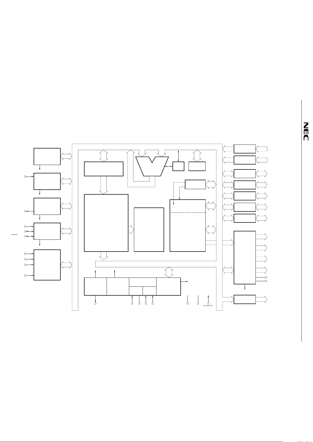
1. PIN CONFIGURATION (TOP VIEW)
S3
S2
S1
S0
P00/INT4
P01/SCK
P02/SO
P03/SI
P10/INT0
P11/INT1
P12/INT2
P13/TI0
P20
P21
P22
P23/BUZ
P30
P31
P32
P33
P60
P61
P62
P63
P40
P41
P42
P43
PPO
X1
X2
V
SS
64
63
62
61
60
59
58
57
56
55
54
53
52
51
50
49
48
47
46
45
44
43
42
41
40
39
38
37
36
35
34
33
1
2
3
4
5
6
7
8
9
10
11
12
13
14
15
16
17
18
19
20
21
22
23
24
25
26
27
28
29
30
31
32
V
DD
S4
S5
S6
S7
S8
S9
V
PRE
V
LOAD
T15/S10
T14/S11
T13/PH0
T12/PH1
T11/PH2
T10/PH3
T9
T8
T7
T6
T5
T4
T3
T2
T1
T0
RESET
P53
P52
P51
P50
XT2
XT1
P41
P42
P43
PPO
X1
X2
V
SS
XT1
XT2
P50
P51
P52
P53
32
31
30
29
28
27
26
25
24
23
22
21
20
P01/SCK
P00/INT4
S0
S1
S2
S3
V
DD
S4
S5
S6
S7
S8
S9
51 50 49 48 47 46 45 44 43 42 41 40 39 38 37 36 35 34 33
1 2 3 4 5 6 7 8 9 10111213141516171819
52
53
54
55
56
57
58
59
60
61
62
63
64
P40
P63
P62
P61
P60
P33
P32
P31
P30
P23/BUZ
P22
P21
P20
P13/TI0
P12/INT2
P11/INT1
P10/INT0
P03/SI
P02/SO
RESET
T0T1T2T3T4T5T6T7T8
T9
V
PRE
T10/PH3
T11/PH2
T12/PH1
T13/PH0
T14/S11
T15/S10
V
LOAD
PD75208CW-× × ×
µ
PD75208GF-× × ×-3BE
µ
6
µ
PD75208
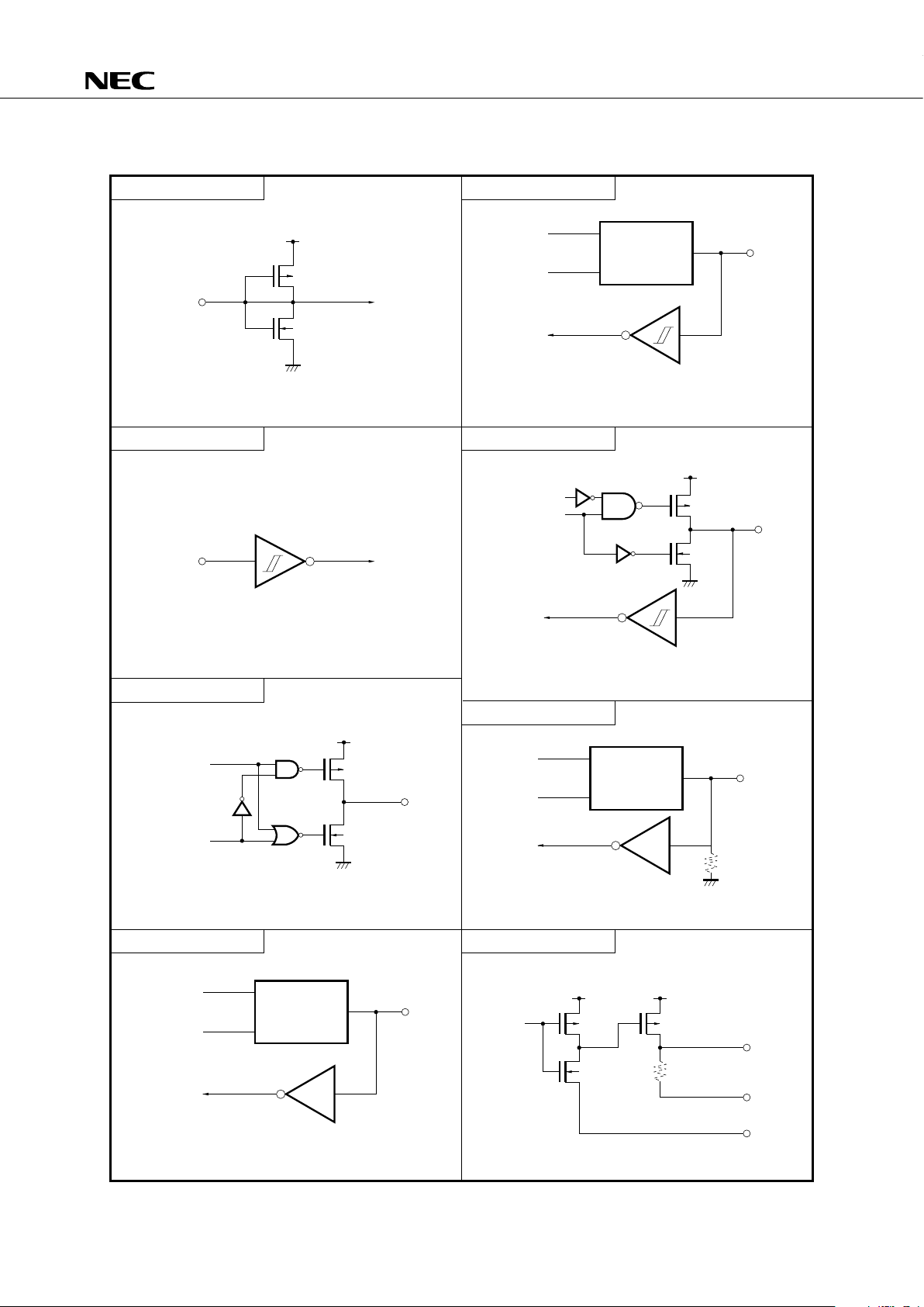
2. BLOCK DIAGRAM
BASIC
INTERVAL
TIMER
TIMER/EVENT
COUNTER
#0
TIMER/PULSE
GENERATOR
INTBT
INTT0
INTTPG
SERIAL
INTERFACE
INTERRUPT
CONTROL
INTSIO
TI0/P13
PPO
SI/P03
SO/P02
SCK/P01
INT0/P10
INT1/P11
INT2/P12
INT4/P00
BUZ/P23
WATCH
TIMER
INTW f
X
/2
N
CLOCK
DIVIDER
SYSTEM CLOCK
GENERATOR
SUB MAIN
STAND BY
CONTROL
XT1 XT2 X1 X2 V
DDVSS
RESET
CPU CLOCK
Φ
PROGRAM
COUNTER(13)
ROM
PROGRAM
MEMORY
8064 × 8 BITS
DECODE
AND
CONTROL
RAM
DATA MEMORY
497 × 4 BITS
GENERAL REG.
BANK
SP(8)CY
ALU
PORT0 4 P00–P03
PORT1 4 P10–P13
PORT2 4 P20–P23
PORT3 4 P30–P33
PORT4 4 P40–P43
PORT5 4 P50–P53
PORT6 4 P60–P63
FIP
CONTROLLER/
DRIVER
10 T0–T9
4
T10/PH3–
T13/PH0
2
T14/S11,T15/
S10
10
S0–S9
V
PRE
V
LOAD
PORTH 4 PH0–PH3
INTKS

7
µ
PD75208
Input
Input
Input
Input/
output
B
F
G
B
INT4
SCK
SO
SI
INT0
INT1
INT2
TI0
–––
–––
–––
BUZ
–––
–––
–––
–––
T13
T12
T11
T10
P00
P01
P02
P03
P10
P11
P12
P13
P20
P21
P22
P23
P30–P33
P40 to P43
P50 to P53
P60 to P63
PH0
PH1
PH2
PH3
3. PIN FUNCTIONS
3.1 PORT PINS
Pin Name I/O After Reset
Input / Output
Circuit Type
*1
Function
DualFunction Pin
8-Bit
I/O
Input/output
Input/output
4-bit input port (PORT0). ×
Input
B
Input
Noise removing function available
Noise removing function available
4-bit input port (PORT1).
4-bit input/output port (PORT2).
Input
E
×
Programmable 4-bit input/ output port (PORT3).
Input/output specifiable in 1-bit units.
Input/
output
Input
E
Input/
output
4-bit input/output port (PORT4).
LED direct drive capability.
●● Input
E
Input/
output
4-bit input/output port (PORT5).
LED direct drive capability.
Input
E
Input/
output
Programmable 4-bit input/output port (PORT6).
Input/output specifiable in 1-bit units.
On-chip pull-down resistor available (mask
option). Suitable for key input.
×
Input V
Output
4-bit P-ch open-drain, high-dielectric, high-current
output port (PORTH).
LED direct drive capability. On-chip pull-down
resistor available (mask option).
×
I
* Schmitt trigger inputs are circled.
Low level
(with an onchip pulldown resistor)
or high
impedance.

8
µ
PD75208
Segment output high voltage output.
Static output also possible.
Pin Name I/O
DualFunction Pin
Input / Output
Circuit Type
*
Function
After Reset
Digit/segment output dual-function
high-voltage high-current output.
Extra pins can be used as PORTH.
Digit output high-voltage high-current
output.
FIP controller/
driver output
pins.
Pull-down
resistor can be
incorporated in
bit units (mask
option).
T0 to T9
Digit/segment output dual-function
high-voltage high-current output.
Static output also possible.
T10 to T13
T14/S11,
T15/S10
S9
Output
–––
PH3 to PH0
–––
Low level
(with an onchip pulldown
resistor ) or
high
impedance
(without a
pull-down
resistor)
I
3.2 NON-PORT PINS
* Schmitt trigger inputs are circled.
B
F
Segment high-voltage output.
S0 to S8
High
impedance
PPO
Output
Input
––– Timer/pulse generator pulse output.
External event pulse input for timer/event counter.
P13
Serial clock input/output.
TI0
SCK
Serial data output pin or serial data input/output.
Serial data input or normal input.
Edge-detected vectored interrupt input (rising and falling
edge detection).
INT0
INT1
SO
SI
INT4
Input/output
Input
Input
Input
P01
P02
P03
P00
P10
P11
Edge-detected vectored interrupt input with noise
eliminate function (detection edge selection possible).
Edge-detected testable input (rising edge detection).
Fixed frequency output (for buzzer or system clock
trimming).
Crystal/ceramic connect pin for main system clock
oscillation.
External clock input to X1 and its inverted clock input to
X2.
Crystal connect pin for subsystem clock oscillation.
External clock input to XT1 and XT2 open.
INT2
Input
Input/output
P12
P23BUZ
X1, X2
XT1
Input
Input
FIP controller/driver output buffer power supply.
FIP controller/driver pull-down resistor connect pin.
GND potential.
XT2
–––
–––
–––
System reset input (low level active).
RESET
VPRE
Input
–––
Positive power supply.
VLOAD
VDD
–––
–––
–––
VSS
D
Input
B
Input
G
Input
B
B
B
B
Input
E
I
I
Input/output
9
µ
PD75208
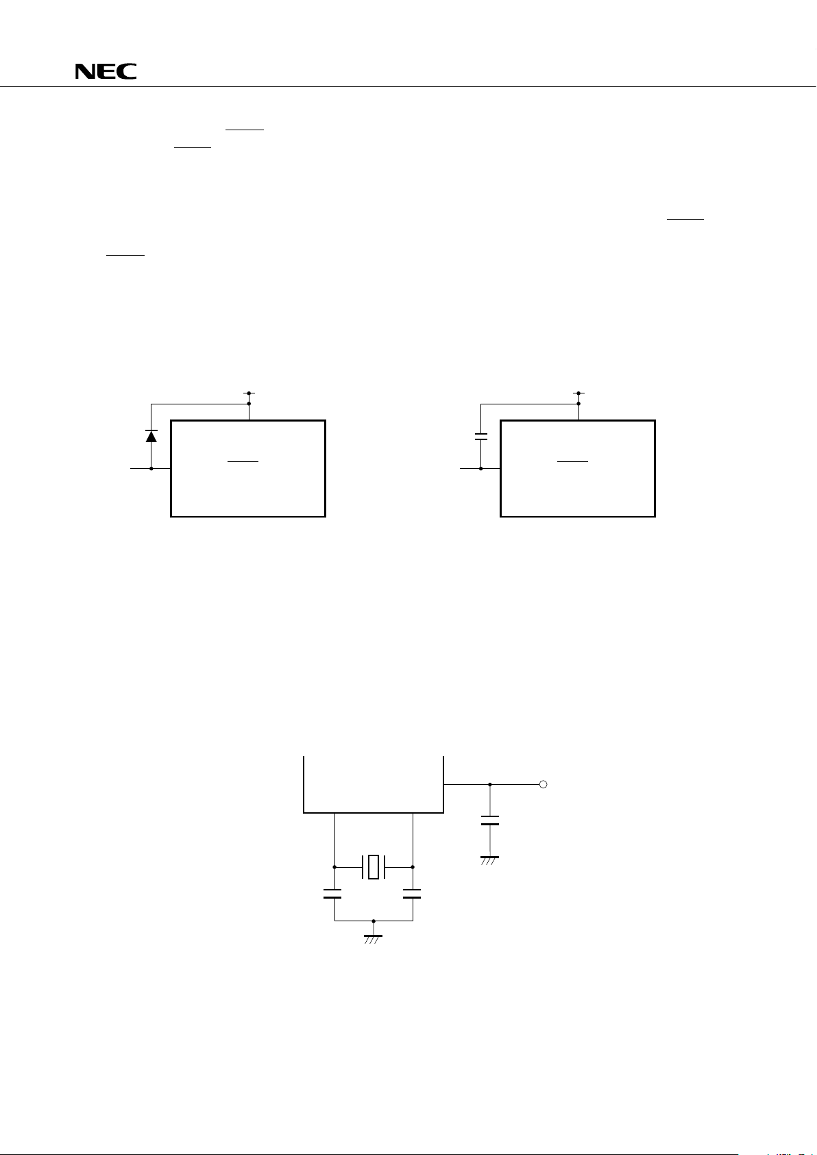
3.3 PIN INPUT/OUTPUT CIRCUIT LIST
TYPE A
TYPE B
TYPE D
TYPE E
TYPE F
TYPE G
TYPE V
TYPE I
V
DD
P-ch
N-ch
IN
IN
V
DD
P-ch
N-ch
OUT
data
output
disable
data
output
disable
Type D
IN/OUT
Type A
data
output
disable
Type D
IN/OUT
Type B
data
output
disable
Type D
IN/OUT
Type A
V
DD
P-ch
N-ch
IN/OUT
data
P-ch output
disable
Type B
V
DD
P-ch
N-ch
OUT
data
V
DD
P-ch
V
LOAD
V
PRE
CMOS-Specified Input Buffer
Schmitt Trigger Input Having Hysteresis Characteristics
Push-Pull Output which can be Set to Output High Impedance
(with Both P-ch and N-ch Set to OFF)
Input/Output Circuit Consisting of Type D Push-Pull Output
and Type A Input Buffer
Pull-down Resistor
(Mask Option)
Pull-down
Resistor
(Mask Option)
Input/Output Circuit Capable of Switching between Push-Pull
Output and N-ch Open-Drain Output (with P-ch OFF).
Input/Output Circuit Consisting of Type D Push-Pull Output
and Type B Schmitt Trigger Input

10
µ
PD75208
3.4 UNUSED PINS TREATMENT
P00/INT4
P01/SCK
P02/SO
P03/SI
P10/INT0 to P12/INT2
P13/TI0
P20 to P22
P23/BUZ
P30 to P33
P40 to P43
P50 to P53
P60 to P63
PPO
S0 to S9
T15/S10 to T14/S11
T0 to T9
T10/PH3 to T13/PH0
XT1
XT2
RESET when there is an on-
chip power-on reset circuit
VLOAD when there is no on-
chip load resistor
Connect to VSS
Connect to VSS or VDD
Connect to VSS
Input state : Connect to VSS or VDD
Output state : Leave open
Leave open
Connect to VSS or VDD
Leave open
Connect to VDD
Connect to VSS or VDD
Recommended ConnectionPin
11
µ
PD75208
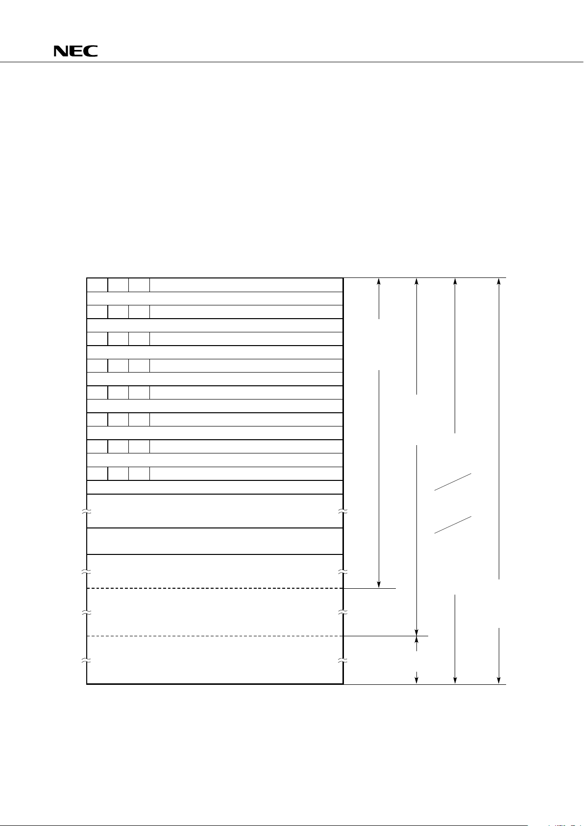
• Connect diode with small VF (0.3 V or less) between
the pins and V
DD
• Connect a capacitor between the pins and VDD.
3.6 XT1, XT2 AND P50 PIN OPERATING PRECAUTIONS
When selecting the 32.768 kHz subsystem clock connected to the XT1 and XT2 pins as the watch timer source
clock, the signal to be input or output to the P50 pin next to the XT2 pin must be a signal required to be switched
between high and low the minimum number of times (once/second or less).
If the P50 pin signal is switched frequently between high and low, a spike is generated in the XT2 pin because
of capacitance coupling of the P50 and XT2 pins and the correct watch functions cannot be achieved (the watch
becomes fast).
If it is necessary to allow the P50 pin signal to switch between high and low, mount an external capacitor to the
P50 pin as shown below.
3.5 P00/INT4 PIN AND RESET PIN OPERATING PRECAUTIONS
P00/INT4 and RESET pins have the function (especially for IC test) to test uPD75208 internal operations in addition
to the functions described in sections 3.1 and 3.2.
The test mode is set when a voltage larger than V
DD is applied to one of these pins. If noise larger than VDD is
applied in normal operation, the test mode may be set thereby adversely affecting normal operation.
Since there is a display output pin having a high-voltage amplitude (35 V) next to the P00/INT4 and RESET pins,
if cables for the related signals are routed in parallel, wiring noise larger than V
DD may be applied to the P00/INT4
and RESET pins causing errors.
Thus, carry out wiring so that wiring noise can be minimized, If noise still cannot be suppressed, take the measure
against noise using the following external components.
V
DD
V
DD
P00/INT4, RESET
V
DD
V
DD
P00/INT4, RESET
XT1
32.768 kHz
0.0068 F
µ
XT2
P50
PD75208
µ
12
µ
PD75208
4. ARCHITECTURE AND MEMORY MAP OF THE µPD75208
The µPD75208 has three architectural features:
• Bank configuration of data memory : Static RAM (448 words × 4 bits)
Display data memory (49 words × 4 bits)
Peripheral hardware (128 × 4 bits)
• Bank configuration of general registers: 8 × 4 banks (for operation in 4-bit units)
4 × 4 banks (for operation in 8-bit units)
• Memory mapped I/O
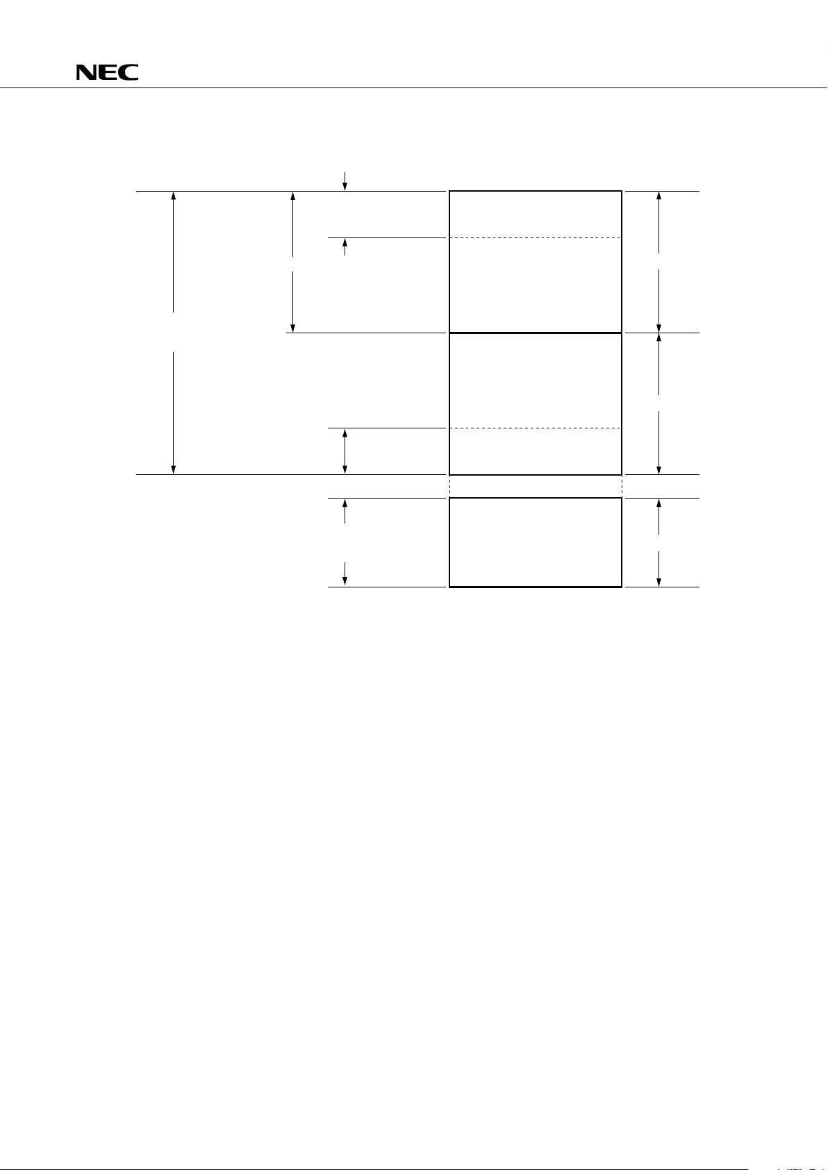
Fig. 4-1 and 4-2 show the memory maps for the
µ
PD75208.
Fig. 4-1 Program Memory Map
Remarks In all cases other than those listed above, branch to the address with only the lower 8 bits of the PC
changed is enabled by BR PCDE and BR PCXA instructions.
MBE RBE 0
765
0000H
Address
MBE RBE 0
0002H
MBE RBE 0
0004H
MBE RBE 0
0006H
MBE RBE 0
0008H
MBE RBE 0
000AH
007FH
0080H
0020H
1F7FH
0
Internal Reset Start Address (High-Order 5 Bits)
Internal Reset Start Address (Low-Order 8 Bits)
INTBT/INT4 Start Address (High-Order 5 Bits)
INTBT/INT4 Start Address (Low-Order 8 Bits)
INT0 Start Address (High-Order 5 Bits)
INT0 Start Address (Low-Order 8 Bits)
INT1 Start Address (High-Order 5 Bits)
INT1 Start Address (Low-Order 8 Bits)
INTSIO Start Address (High-Order 5 Bits)
INTSIO Start Address (Low-Order 8 Bits)
INTT0 Start Address (High-Order 5 Bits)
INTT0 Start Address (Low-Order 8 Bits)
NTTPG Start Address (High-Order 5 Bits)
INTTPG Start Address (Low-Order 8 Bits)
INTKS Start Address
(High-Order 5 Bits)
INTKS Start Address
(Low-Order 8 Bits)
GETI Instruction Reference Table
000EH
MBE RBE 0
MBE RBE 0
000CH
07FFH
0800H
0FFFH
1000H
BRCB
! caddr Instruction
Branch Address
CALL ! addr
Instruction
Subroutine Entry
Address
BR ! addr
Instruction Branch
Address
BR $addr
Instruction
Relative Branch
Address
(–15 to –1,
+2 to +16)
BRCB
! caddr
Instruction
Branch
Address
CALLF
! faddr
Instruction
Entry
Address
Branch Destination
Address Specified
by GETI Instruction,
Subroutine Entry
Address
13
µ
PD75208
Fig. 4-2 Data Memory Map
(32 × 4)
256 × 4
(49 × 4)
241 × 4
128 × 4
Not Incorporated
F80H
FFFH
1FFH
1C0H
1BFH
100H
0FFH
020H
000H
General
Register
Area
Display Data
Memory,
etc.
01FH
General
Static RAM
(497 × 4)
Stack Area
Peripheral
Hardware
Area
Bank 0
Bank 1
Bank 15

14
µ
PD75208
5. PERIPHERAL HARDWARE FUNCTIONS
5.1 PORTS
The
µ
PD75208 has the following three types of I/O port:
• 8 CMOS input ports
• 20 CMOS I/O ports
• 4 P-ch open-drain high-voltage, large-current output ports
Total: 32 ports
Table 5-1 Functions of Ports
Remarks
Port Name
Always read or test possible irrespective of the dual-function
pin operating mode.
Always read or test possible, P10 and P11 are inputs with the
noise eliminate function.
Can be set to the input or output mode in 4-bit units.
Ports 4 and 5 can input/output data in pairs in 8-bit units.
Ports 4 and 5 can directly drive LEDs.
Can be set bit-wise to the input or output mode. Port 6 can
incorporate a pull-down resistor as a mask option.
P-ch open-drain high-voltage, high-current output port. Can
drive an FIP and LED directly. Can incorporate a pull-down
resistor bit-wise as a mask option.
Shares the pins with SI, SO, SCK
and INT4.
Shares the pins with INT0 to 2
and TI0.
P23 shares the pin with BUZ.
Shares the pins with T10 to T13.
Operation and Feature
Function
4-bit input
PORT0
PORT1
PORT2
PORT4
PORT5
PORT3
PORT6
4-bit
input/output
PORTH
4-bit output
15
µ
PD75208
5.2 CLOCK GENERATOR
Operation of the clock generator is specified by the processor clock control register (PCC) and system clock control
register (SCC).
The main system clock or subsystem clock can be selected.
The instruction execution time is variable.
• 0.95
µ
s, 1.91 µs, 15.3 µs (main system clock: 4.19 MHz)
• 122
µ
s (subsystem clock: 32.768 kHz)
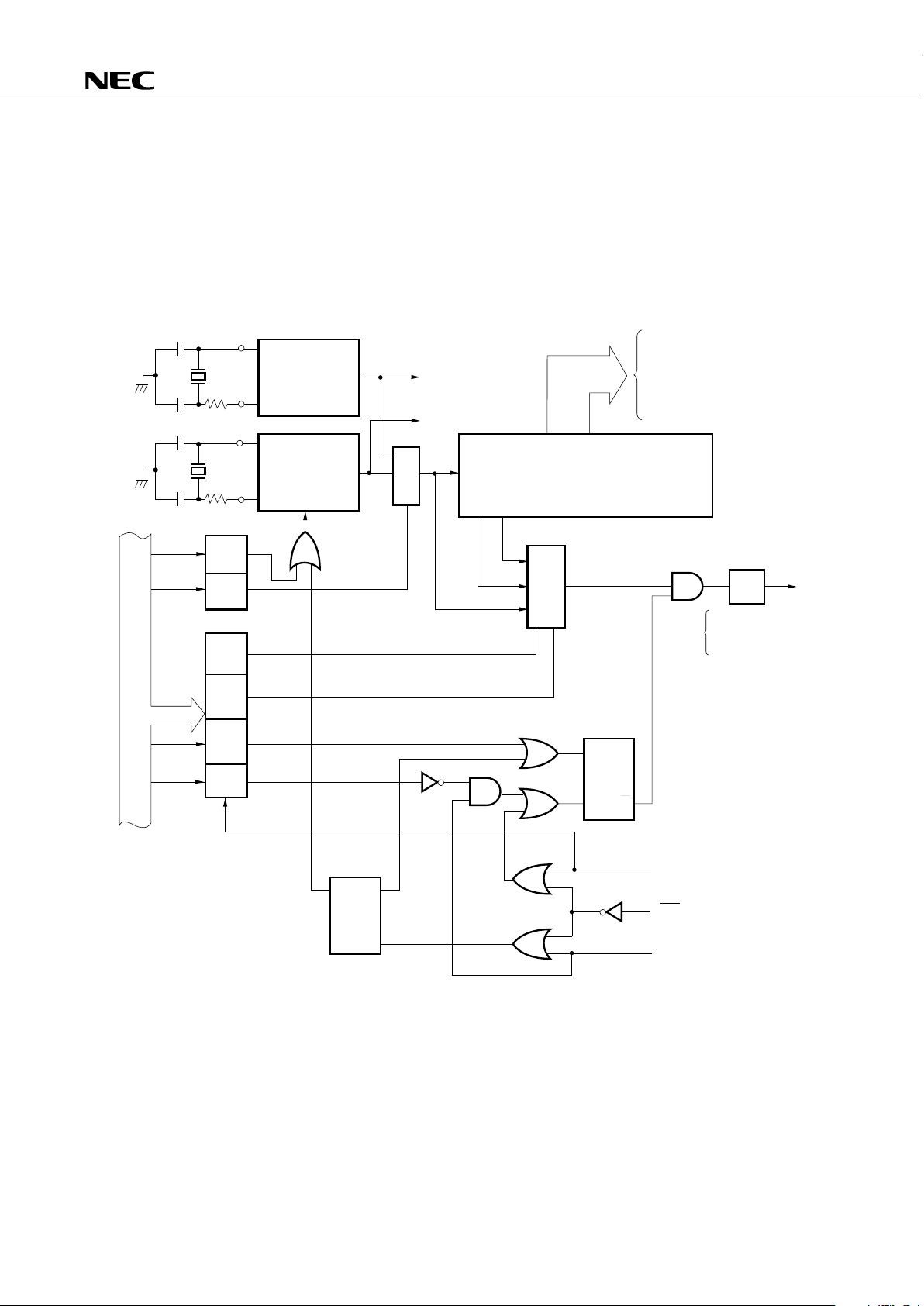
Fig. 5-1 Clock Generator Block Diagram
* Instruction execution
Remarks 1. f
X = Main system clock frequency
2. f
XT = Subsystem clock frequency
3. f
XX = System clock frequency
4.
Φ
= CPU clock
5. PCC: Processor clock control register
6. SCC: System clock control register
7. 1 clock cycle (t
CY) of
Φ
is 1 machine cycle of an instruction. For tCY, see ”AC Characteristics“ in
12. ELECTRICAL SPECIFICATIONS.
★
XT1
XT2
X1
X2
f
XT
f
X
SCC
PCC
HALT*
STOP*
HALT F/F
STOP F/F
4
QS
R
S
R
1/4
1/8 to 1/4096
SCC3
SCC0
PCC0
PCC1
PCC2
PCC3
Q
Selector
f
XX
1/2 1/6
Frequency Divider
Selector
Watch Timer
Timer/Pulse
Generator
Subsystem
Clock
Generator
Main System
Clock
Generator
Oscillation
Stop
Frequency
Divider
• FIP Controller
• Basic Interval Timer (BT)
• Timer/Event Counter
• Serial Interface
• Watch Timer
• INT0 Noise Eliminator
• CPU
• INT0 Noise Eliminator
• INT1 Noise Eliminator
Φ
Wait Release Signal from BT
RES Signal (Internal Reset)
Standby Release Signal from
Interrupt Control Circuit
PCC2 and
PCC3
Clear
Internal Bus
16
µ
PD75208
5.3 BASIC INTERVAL TIMER
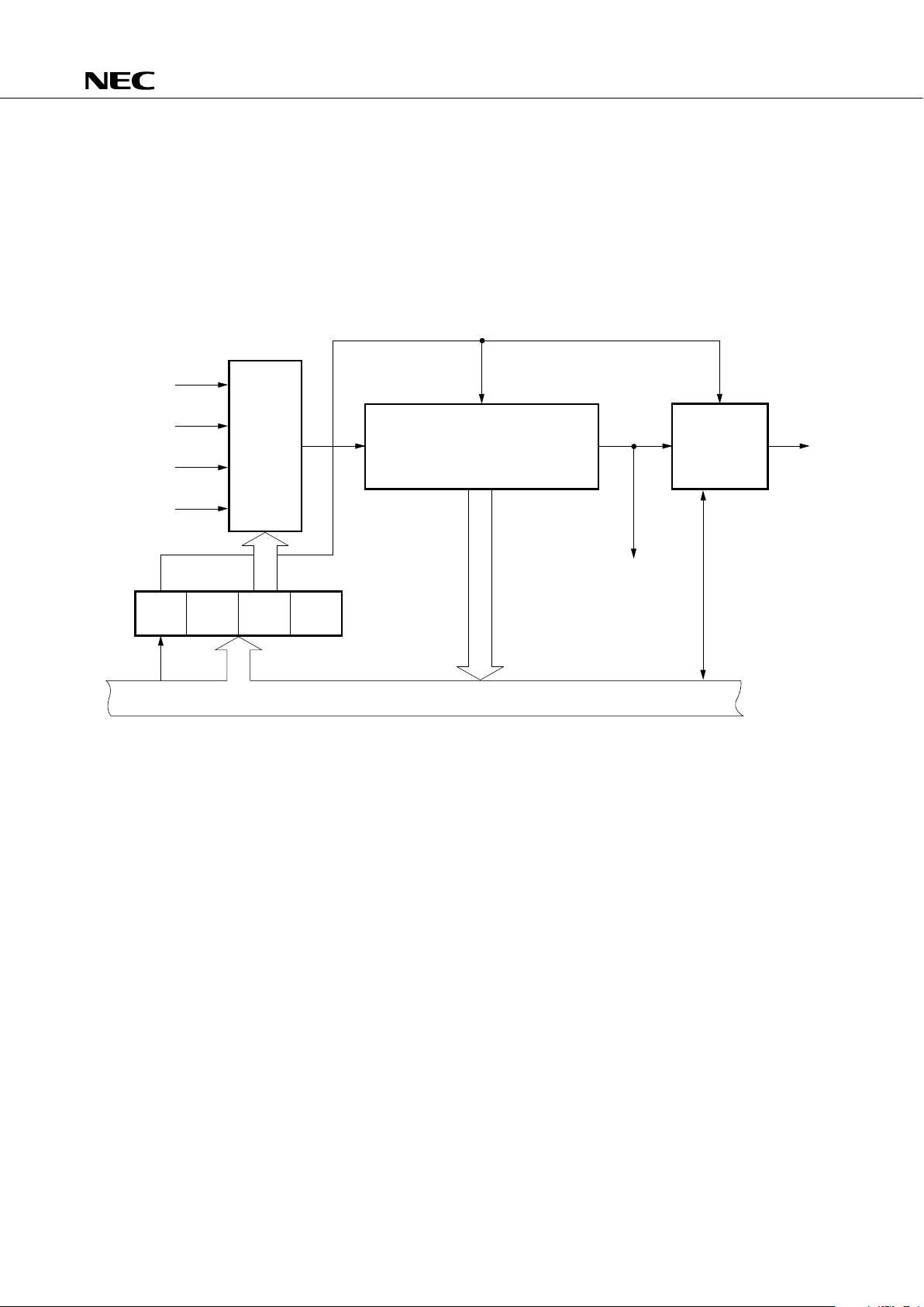
The basic interval timer has the following functions:
• Interval timer operation to generate reference time
• Watchdog timer application to detect inadvertent program loop
• Wait time select and count upon standby mode release
• Count contents read
Fig. 5-2 Basic Interval Timer Configuration
* Instruction execution
Internal Bus
f
XX
/2
5
fXX/2
7
fXX/2
12
From Clock
Generator
4
BTM3 BTM2 BTM1 BTM0 BTM
MPX
BT IRQBT
Set
BT Interrupt
Request Flag
Clear Clear
Basic Interval Timer
(8-Bit Frequency Divider)
Wait Release
Signal during
Standby Release
8
3
Vectored
Interrupt
Request
Signal
f
XX
/2
9
SET1*
17
µ
PD75208
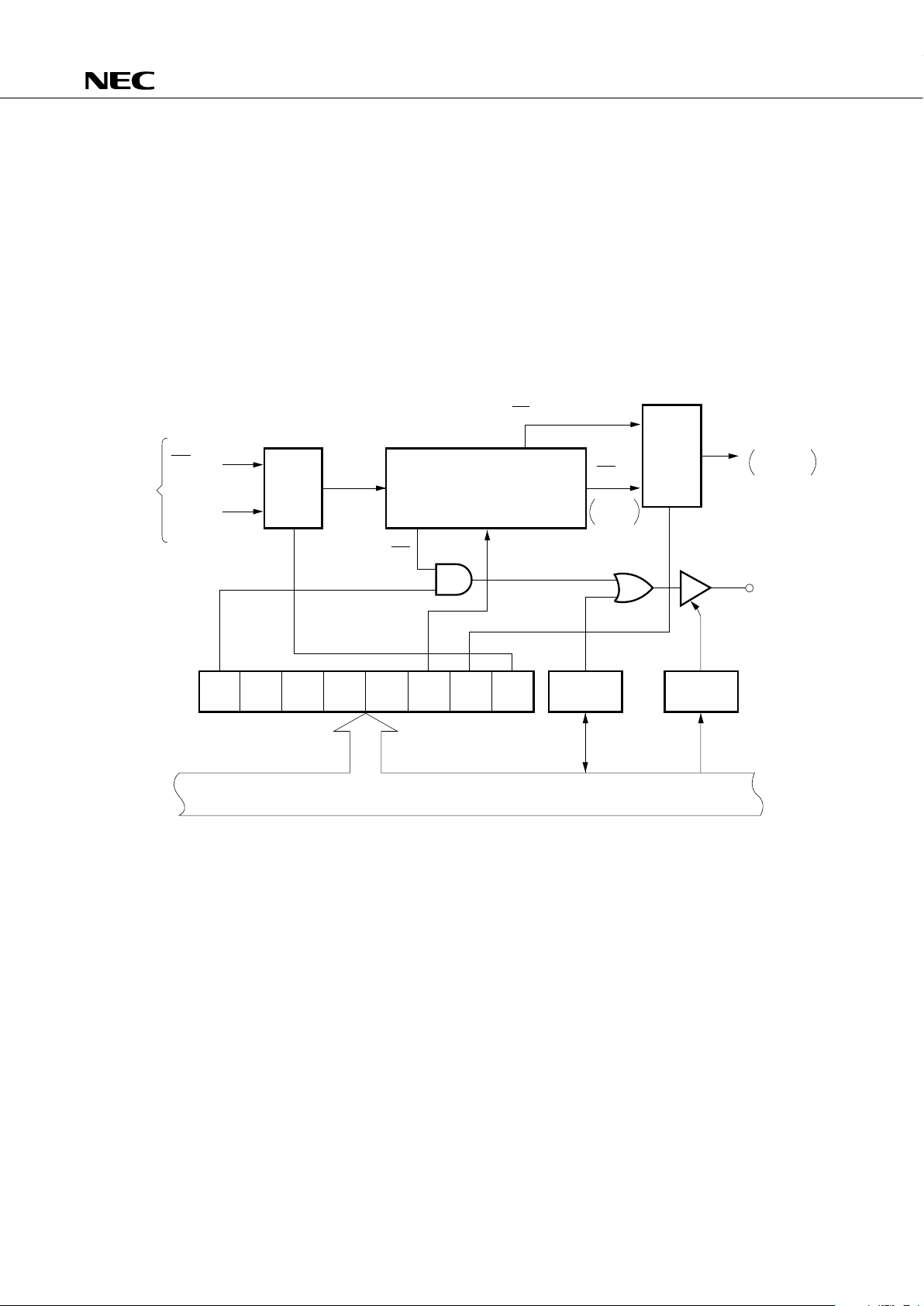
5.4 WATCH TIMER
The
µ
PD75208 incorporates one channel of watch timer. The watch timer has the following functions:
• Sets the test flag (IRQW) at 0.5 sec intervals.
The standby mode can be released by IRQW.
• 0.5 second interval can be set with the main system clock and subsystem clock.
• The fast mode enables to set 128-time (3.91 ms) interval useful to program debugging and inspection.
• The fixed frequencies (2.048 kHz) can be output to the P23/BUZ pin for use to generate buzzer sound
and trim the system clock oscillator frequency.
• Since the frequency divider can be cleared, the watch can be started from zero second.
Fig. 5-3 Watch Timer Block Diagram
Remarks Values at f
XX = 4.194304 MHz and fXT = 32.768 kHz are indicated in parentheses.
8
Internal Bus
WM7 WM6 WM5 WM4 WM2 WM1 WM0
P23
Output
Latch
Port 2
Input/Output
Mode
PORT2.3 Bit 2 of PMGB
P23/BUZ
Output Buffer
Selector
Frequency Divider
Clear
(2.048 kHz)
2
14
f
W
2
7
f
W
(256 Hz : 3.91 ms)
f
W
(32.768 kHz)
Selector
WM
From
Clock
Generator
16
f
W
128
f
XX
(32.768 kHz)
f
XT
(32.768 kHz)
INTW
IRQW
Set Signal
2Hz
0.5 sec
WM3
18
µ
PD75208
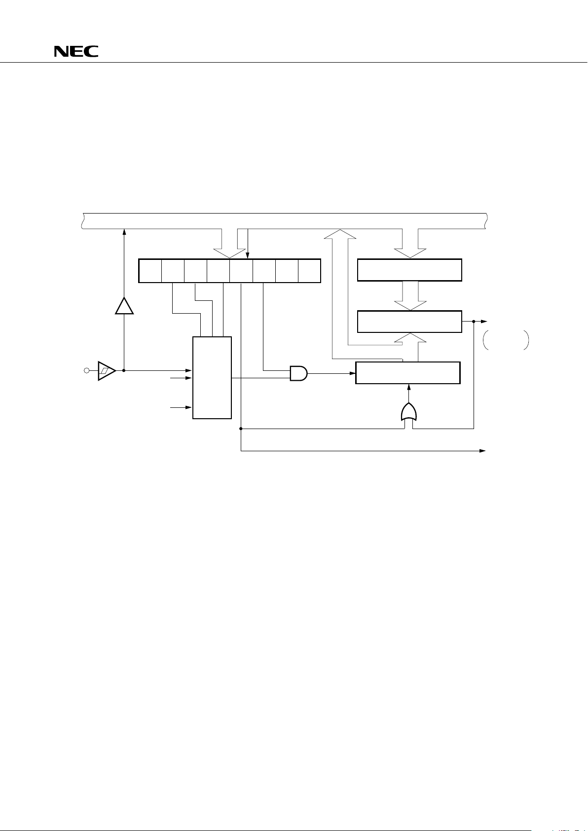
5.5 TIMER/EVENT COUNTER
The
µ
PD75208 incorporates one channel of timer/event counter. The timer/event counter has the following
functions:
• Program interval timer operation
• Event counter operation
• Count state read function
Fig. 5-4 Timer/Event Counter Block Diagram
* Instruction execution
P13/TI0
Input Buffer
From Clock
Generator
MPX
TMn6 TMn5 TMn4 TMn3 TMn2
SET1
TM0
Timer Operation Start
CP
Count Register (8)
Clear
8
Comparator (8)
8
8
Modulo Register (8)
8
8
Internal Bus
TMOD0
Match
IRQT0
Clear
T0
TMn7 TMn1 TMn0
*
INTT0
IRQT0
Set Signal
(Refer to Fig. 5-1)
19
µ
PD75208
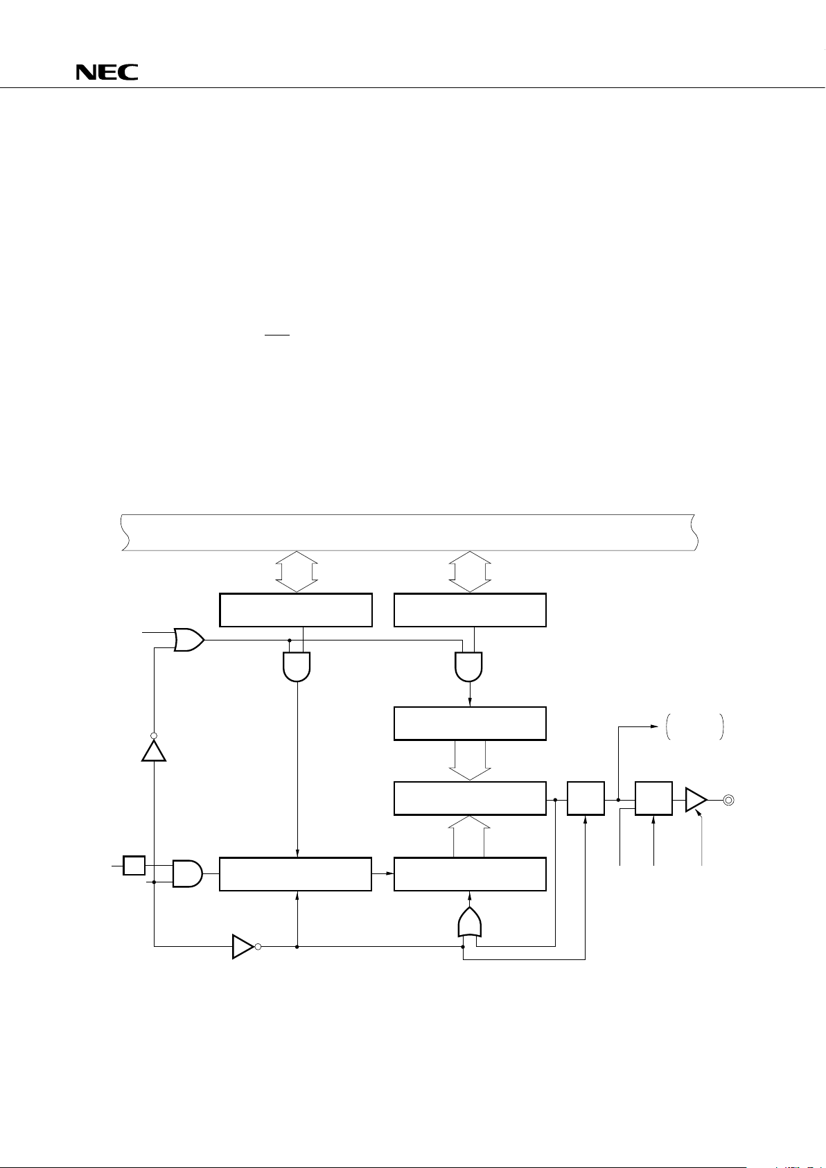
5.6 TIMER/PULSE GENERATOR
The
µ
PD75208 incorporates one channel of timer/pulse generator which can be used as a timer or a pulse
generator. The timer/pulse generator has the following functions:
(a) Functions available in the timer mode
• 8-bit interval timer operation (IRQTPG generation) enabling the clock source to be varied at 5 levels
• Square wave output to PPO pin
(b) Functions available in the PWM pulse generate mode
• 14-bit accuracy PWM pulse output to the PPO pin (Used as a digital-to-analog converter and applicable
to tuning)
• Fixed time interval ( = 7.81 ms : at 4.19 MHz operation) interrupt generation
If pulse output is not necessary, the PPO pin can be used as a 1-bit output port.
Note If the STOP mode is set while the timer/pulse generator is in operation, erroneous operation may result.
To prevent that from occurring, preset the timer/pulse generator to the stop state using its mode
register.
Fig. 5-5 Block Diagram of Timer/Pulse Generator (Timer Mode)
2
15
fXX
88
MODL MODH
TPGM3
8
8
1/2
f
X
TPGM1
CP
TPGM4 TPGM5 TPGM7
PPO
INTTPG
Internal Bus
Modulo Register L (8) Modulo Register H (8)
Modulo Latch H (8)
Comparator (8)
Count Register (8)
Clear
Prescalar Select Latch (5)
Clear
Frequency
Divider
(Set to "1")
Set
T F/F
Selector
Output Buffer
IRQTPG
Set Signal
Match
 Loading...