NEC UPD17P719GC-3B9 Datasheet

DATA SHEET
MOS INTEGRATED CIRCUIT
µ
PD17P719
4-BIT SINGLE-CHIP MICROCONTROLLER WITH
BUILT-IN HARDWARE DEDICATED TO DIGITAL TUNING SYSTEMS
The µPD17P719 is produced by replacing the built-in masked ROM of the µPD17717, µPD17718, and µPD17719
with a one-time PROM.
µ
PD17P719 allows programs to be written once, so that the µPD17P719 is suitable for preproduction in
The
µ
PD17717, µPD17718, or µPD17719 system development or low-volume production.
µ
When reading this document, also refer to the publications on the
The electrical characteristics (including power supply currents) and PLL analog characteristics of
the µPD17P719 differ from those of the µPD17717, µPD17718, and µPD17719. In high-volume application
set production, carefully check those differences.
PD17717, µPD17718, or µPD17719.
FEATURES
• Compatible with the µPD17717, µPD17718, and µPD17719
• Built-in one-time PROM : 32K bytes (16384 × 16 bits)
• Supply voltage : PLL operation : VDD = 4.5 to 5.5 V
CPU operation: VDD = 3.5 to 5.5 V
ORDERING INFORMATION
Part number Package
µ
PD17P719GC-3B9 80-pin plastic QFP (14 × 14 mm, 0.65-mm pitch)
The information in this document is subject to change without notice.
Document No. U12112EJ1V0DS00 (1st edition)
Date Published February 1997 J
Printed in Japan
©
1997

µ
PD17P719
FUNCTION OVERVIEW
Item
Program memory (ROM)
General-purpose data
memory (RAM)
Instruction execution time
General-purpose ports
Stack level
Interrupt
Timers
A/D converter
D/A converter
(PWM)
Serial interface
Frequency
PLL
division
system
Reference
frequency
Charge pump
Phase comparator
Intermediate frequency
counter
Product
µ
µ
µ
PD17717
12288 × 16 bits
(masked ROM)
1120 × 4 bits
1.78 µs (with fX = 4.5-MHz crystal)
• I/O ports : 46
• Input ports : 12
• Output ports : 4
• Address stack : 15 levels
• Interrupt stack: 4 levels
• DBF stack : 4 levels (operated by software)
• External : 6 (CE rising edge and INT0 to INT4)
• Internal : 6 (timers 0 to 3, serial interfaces 0 and 1)
5 channels
• Basic timer (clock: 10, 20, 50, 100 Hz) : 1 channel
• 8-bit timer with gate counter (clock: 1 k, 2 k, 10 k, 100 kHz) : 1 channel
• 8-bit timer (clock: 1 k, 2 k, 10 k, 100 kHz) : 2 channels
• 8-bit timer, also used for PWM (clock: 440 Hz, 4.4 kHz) : 1 channel
8 bits × 6 channels (Hardware or software mode can be selected.)
3 channels (8-bit or 9-bit resolution, selected by software.)
Output frequency: 4.4 kHz, 440 Hz (8-bit PWM)
2.2 kHz, 220 Hz (9-bit PWM)
2 systems (4 channels)
• Selectable for 3-wire serial I/O method, SBI method, 2-wire serial I/O method, or I2C bus
Note
method
• Selectable for 3-wire serial I/O method or UART method.
• Direct frequency division system (VCOL pin (MF mode) : 0.5 to 3 MHz)
• Pulse swallow system (VCOL pin (HF mode) : 10 to 40 MHz)
Can be set to one of 13 frequencies
(1, 1.25, 2.5, 3, 5, 6.25, 9, 10, 12.5, 18, 20, 25, or 50 kHz).
2 error output pins (EO0 and EO1)
Unlock detection is enabled by software.
• Intermediate frequency (IF) measurement
P1C0/FMIFC pin : 10 to 11 MHz in FMIF mode
P1C1/AMIFC pin : 0.4 to 0.5 MHz in AMIF mode
• External gate width measurement
P2A1/FCG1 and P2A0/FCG0 pins
.
µ
PD17718
16384 × 16 bits
(masked ROM)
(VCOH pin (VHF mode): 60 to 130 MHz)
0.4 to 0.5 MHz in AMIF mode
PD17719
1776 × 4 bits
PD17P719
16384 × 16 bits
(one-time PROM)
(1/2)
Note When ordering a mask, please consult our sales office if the I2C bus method is used (or when the serial
interface is accomplished by the program not by the peripheral hardware).
2

µ
PD17P719
(2/2)
Item
BEEP output
Reset
Standby
Supply voltage
Package
Product
µ
µ
µ
µ
PD17717
2
Output frequency : 1 kHz, 3 kHz, 4 kHz, 6.7 kHz (BEEP0 pin)
67 Hz, 200 Hz, 3 kHz, 4 kHz (BEEP1 pin)
• Power-on reset (when the power is turned on)
• Reset using the RESET pin
• Watchdog timer reset
Can be set only once at power-on: 65,536 instructions, 131,072 instructions, or non-use
can be selected.
• Stack pointer overflow/underflow reset
Can be set only once at power-on: the interrupt stack or address stack can be selected.
• CE reset (CE pin: low → high)
A CE reset delay timing can be set.
• Power-failure detection function
• Clock stop mode (STOP)
• Halt mode (HALT)
• PLL operation : VDD = 4.5 to 5.5 V
• CPU operation: VDD = 3.5 to 5.5 V
80-pin plastic QFP (14 × 14 mm, 0.65-mm pitch)
PD17718
PD17719
PD17P719
3

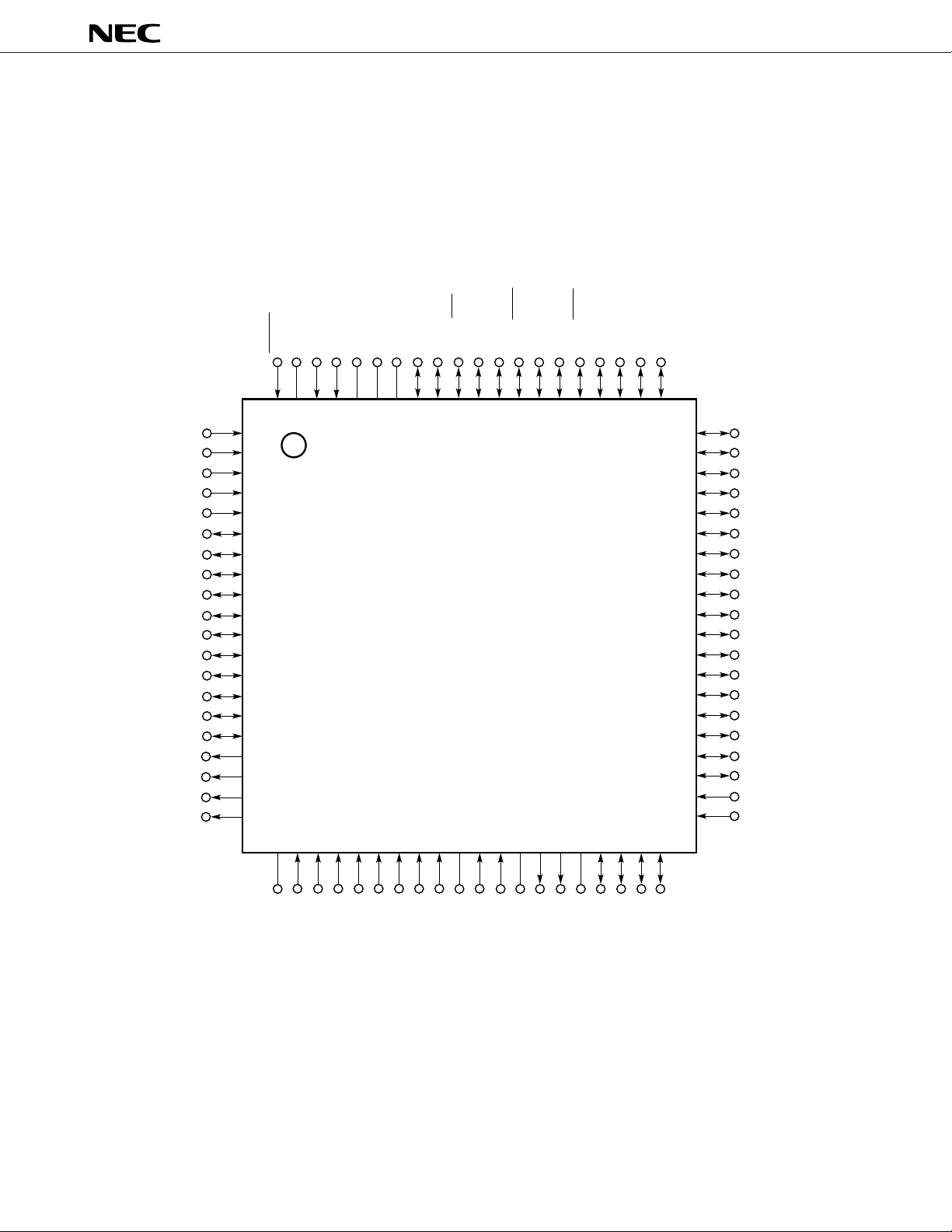
PIN CONFIGURATION (TOP VIEW)
80-pin plastic QFP (14 × 14 mm, 0.65-mm pitch)
µ
PD17P719GC-3B9
(1) Normal operation mode
0
DD
INXOUT
GND0
X
INT2
P1A3/INT4
P1A2/INT3
P1A1
P1A0/TM0G
P3A3
P3A2
P3A1
P3A0
P3B3
P3B2
P3B1
P3B0
P2A2
P2A1/FCG1
P2A0/FCG0
P1B3
P1B2/PWM2
P1B1/PWM1
P1B0/PWM0
CE
RESET
V
80 79 78 77 76 75 74 73 72 71 70 69 68 67 66 65 64 63 62 61
1
2
3
4
5
6
7
8
9
10
11
12
13
14
15
16
17
18
19
20
REG
P2D0/SB0
P2D1/SB1
P2D2/SCK
P0B0/SI3/RxD
P0B1/SO3/TxD
P0B2/SCK3/ASCK
P0B3/SI2
P0A0/SO2
P0A1/SCK2
P0A2/SCL
P0A3/SDA
P0C0
P0C1
60
59
58
57
56
55
54
53
52
51
50
49
48
47
46
45
44
43
42
41
µ
PD17P719
P0C2
P0C3
P2C0
P2C1
P2C2
P2C3
P3D0
P3D1
P3D2
P3D3
P3C0
P3C1
P3C2
P3C3
P2B0
P2B1
P2B2
P2B3
INT0
INT1
22 23 24 25 26 27 28 29 30 31 32 33 34 35 36 37 38 39 40
21
1
GND2
P0D3/AD3
P0D2/AD2
P0D1/AD1
P0D0/AD0
P1C3/AD5
P1C2/AD4
P1C1/AMIFC
DD
V
VCOH
P1C0/FMIFC
VCOL
GND1
EO0
EO1
TEST
P1D3
P1D2
P1D1/BEEP1
P1D0/BEEP0
4

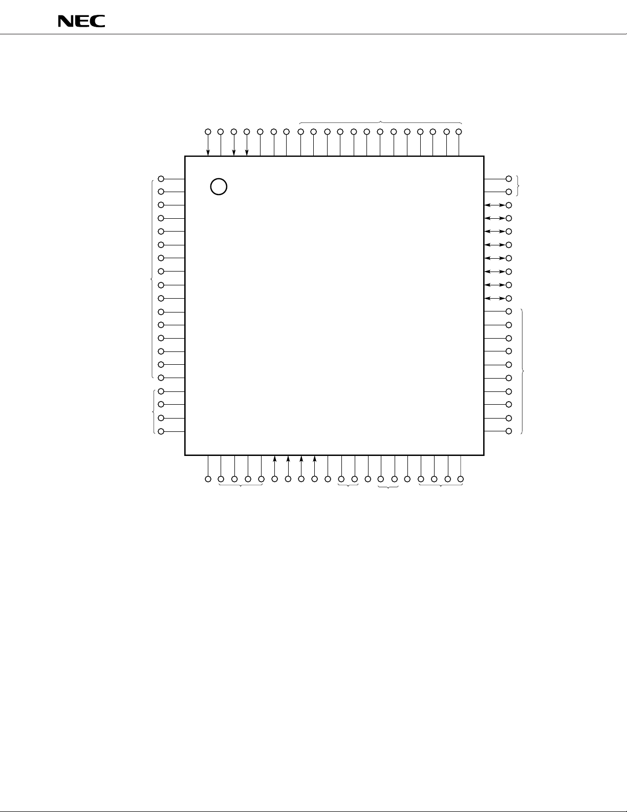
(2) PROM programming mode
µ
PD17P719
(L)
(OPEN)
(OPEN)
GND0
Note
REG
(L)
0
DD
(L)
(H)
80 79 78 77 76 75 74 73 72 71 70 69 68 67 66 65 64 63 62 61
1
2
3
4
5
6
7
8
9
10
11
12
13
14
15
16
17
18
19
20
CLK
V
60
59
58
57
56
55
54
53
52
51
50
49
48
47
46
45
44
43
42
41
(L)
D0
D1
D2
D3
D4
D5
D6
D7
(L)
22 23 24 25 26 27 28 29 30 31 32 33 34 35 36 37 38 39 40
21
(L)
GND2
Note Connect to the same potential as V
MD3
DD.
MD2
MD1
MD0
1
(L)
DD
V
GND1
PP
V
(OPEN)
(L)
Caution The parentheses above indicate the handling of the pins not used in PROM programming mode.
L : Connect each pin to GND through a resistor (470 ohms).
H : Connect each pin to V
DD through a resistor (470 ohms).
OPEN : Leave each pin open.
5

PIN NAMES
µ
PD17P719
AD0-AD5 : A/D converter inputs
AMIFC : AM frequency counter input
ASCK : UART serial clock I/O
BEEP0, BEEP1 : Beep outputs
CE : Chip enable
CLK : Address update clock input
D0-D7 : Data I/O
EO0, EO1 : Error outputs
FCG0, FCG1 : Frequency counter gate inputs
FMIFC : FM frequency counter input
GND0-GND2 : Ground 0 to 2
INT0-INT4 : External interrupt inputs
MD0-MD3 : Operating mode selection
PWM0-PWM2 : D/A converter outputs
P0A0-P0A3 : Port 0A
P0B0-P0B3 : Port 0B
P0C0-P0C3 : Port 0C
P0D0-P0D3 : Port 0D
P1A0-P1A3 : Port 1A
P1B0-P1B3 : Port 1B
P1C0-P1C3 : Port 1C
P1D0-P1D3 : Port 1D
P2A0-P2A2 : Port 2A
P2B0-P2B3 : Port 2B
P2C0-P2C3 : Port 2C
P2D0-P2D2 : Port 2D
P3A0-P3A3 : Port 3A
P3B0-P3B3 : Port 3B
P3C0-P3C3 : Port 3C
P3D0-P3D3 : Port 3D
REG : CPU regulator
RESET : Reset input
RxD : UART serial data input
SB0, SB1 : SBI serial data I/O
SCK : SBI serial clock I/O
SCK2, SCK3 : 3-wire serial clock I/O
SCL : 2-wire serial clock I/O
SDA : 2-wire serial data I/O
SI2, SI3 : 3-wire serial data input
SO2, SO3 : 3-wire serial data output
TEST : Test input
TM0G : Timer 0 gate input
TxD : UART serial data output
VCOH : Local oscillation high input
VCOL : Local oscillation low input
DD0, VDD1 : Power supply
V
PP : Program voltage application
V
XIN, XOUT : Main clock oscillation
6

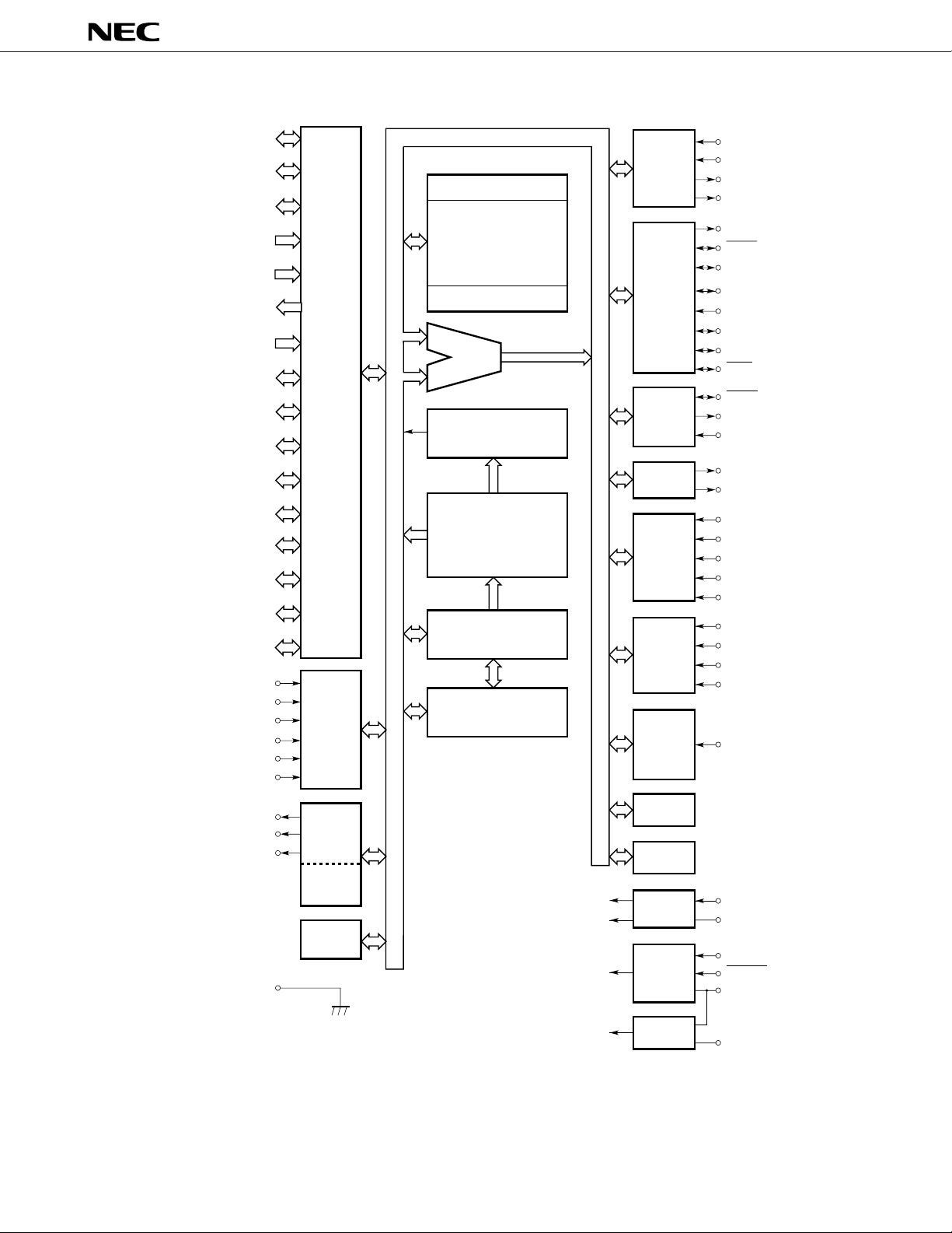
BLOCK DIAGRAM
µ
PD17P719
P0A0-P0A3
P0B0-P0B3
P0C0-P0C3
P0D0-P0D3
P1A0-P1A3
P1B0-P1B3
P1C0(MD0)-
P1C3(MD3)
P1D0-P1D3
P2A0-P2A2
P2B0-P2B3
P2C0(D0)-P2C3(D3)
P2D0-P2D2
P3A0-P3A3
P3B0-P3B3
P3C0-P3C3
P3D0(D4)-P3D3(D7)
AD0/P0D0
AD1/P0D1
AD2/P0D2
AD3/P0D3
AD4/P1C2
AD5/P1C3
PWM0/P1B0
PWM1/P1B1
PWM2/P1B2
GND0-GND2
4
4
4
4
4
4
4
4
3
4
4
3
4
4
4
4
Ports
A/D
converter
D/A
converter
8-bit
timer 3
Basic
timer
RF
RAM
1776 × 4 bits
SYSREG
ALU
Instruction
decoder
One-time PROM
16384 × 16 bits
Program counter
Stack
CPU
Peripheral
PLL
Serial
interface 2
Serial
interface 3
BEEP
Interrupt
control
Frequency
counter
8-bit
timer 0
Gate
counter
8-bit
timer 1
8-bit
timer 2
OSC
Reset
VCOH
VCOL
EO0
EO1
SO2/P0A0
SCK2/P0A1
SCL/P0A2
SDA/P0A3
SI2/P0B3
SB0/P2D0
SB1/P2D1
SCK/P2D2
SCK3/P0B2/ASCK
SO3/P0B1/TxD
SI3/P0B0/RxD
BEEP0/P1D0
BEEP1/P1D1
INT0
INT1
INT2
INT3/P1A2
INT4/P1A3
FCG0/P2A0
FCG1/P2A1
FMIFC/P1C0
AMIFC/P1C1
TM0G/P1A0
X
IN
(CLK)
X
OUT
CE
RESET
VDD0,VDD1
V
CPU
Regurator
Remark Pins enclosed in parentheses are used in PROM programming mode.
REG
7

µ
PD17P719
CONTENTS
1. PIN FUNCTIONS......................................................................................................................... 9
1.1 NORMAL OPERATION MODE ....................................................................................................... 9
1.2 PROM PROGRAMMING MODE..................................................................................................... 13
1.3 EQUIVALENT CIRCUIT OF PINS .................................................................................................. 14
1.4 HANDLING UNUSED PINS ............................................................................................................ 19
1.5 NOTES ON USE OF THE CE, INT0-INT4, AND RESET PINS (ONLY IN NORMAL
OPERATION MODE) ....................................................................................................................... 21
1.6 NOTES ON USE OF THE TEST PIN (ONLY IN NORMAL OPERATION MODE) ...................... 21
2. ONE-TIME PROM (PROGRAM MEMORY) WRITE, READ, AND VERIFICATION................ 22
2.1 OPERATING MODES FOR PROGRAM MEMORY WRITE, READ, AND VERIFICATION ........ 23
2.2 PROGRAM MEMORY WRITE PROCEDURE ............................................................................... 24
2.3 PROGRAM MEMORY READ PROCEDURE................................................................................. 25
3. ELECTRICAL CHARACTERISTICS .......................................................................................... 26
4. PACKAGE DRAWING ................................................................................................................ 31
5. RECOMMENDED SOLDERING CONDITIONS....................................................................... 32
APPENDIX DEVELOPMENT TOOLS.............................................................................................. 33
8

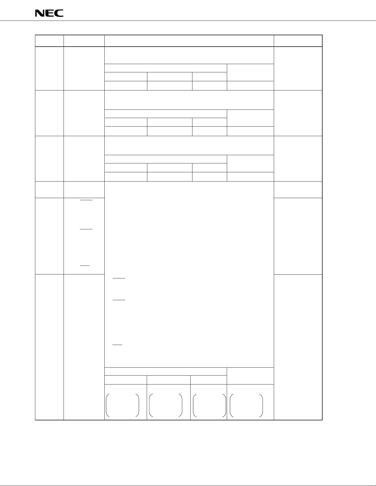
1. PIN FUNCTIONS
1.1 NORMAL OPERATION MODE
µ
PD17P719
Pin No.
1
41
42
2
3
4
5
6
to
9
10
to
13
14
15
16
Symbol
INT2
INT1
INT0
P1A3/INT4
P1A2/INT3
P1A1
P1A0/TM0G
P3A3
to
P3A0
P3B3
to
P3B0
P2A2
P2A1/FCG1
P2A0/FCG0
Input for edge-detected vectored. Either a rising edge or falling edge
can be selected.
Input for port 1A, external interrupt request signal, and event signal
• P1A3-P1A0
• 4-bit input port
• INT4, INT3
• Edge-detected vectored interrupt
• TM0G
• Gate input for 8-bit timer 0
When reset
Power-on reset WDT&SP reset
Input
(P1A3-P1A0)
4-bit I/O port.
Input/output can be specified in 4-bit units.
Power-on reset WDT&SP reset
Input
4-bit I/O port.
Input/output can be specified in 4-bit units.
Power-on reset WDT&SP reset
Input
Input for port 2A and external gate counter
Input
(P1A3-P1A0)
When reset
Input
When reset
Input
Held
Held
Held
CE reset
CE reset
CE reset
When the clock
is stopped
Held
When the clock
is stopped
Held
When the clock
is stopped
Held
• P2A2-P2A0
• 3-bit I/O port
• Input/output can be specified bit by bit.
• FCG1, FCG0
• External gate counter input
Output formatFunction
-
-
CMOS push-pull
CMOS push-pull
CMOS push-pull
When reset
Power-on reset WDT&SP reset
Input
(P2A2-P2A0)
Input
(P2A2-P2A0)
CE reset
Held
(P2A2-P2A0)
When the clock
is stopped
Held
(P2A2-P2A0)
9

µ
PD17P719
Pin No.
17
18
to
20
21
33
75
22
to
25
26
27
28
29
Symbol
P1B3
P1B2/PWM2
to
P1B0/PWM0
GND2
GND1
GND0
P0D3/AD3
to
P0D0/AD0
P1C3/AD5
P1C2/AD4
P1C1/AMIFC
P1C0/FMIFC
Function
Output for port 1B and D/A converter
• P1B3-P1B0
• 4-bit output port
• PWM2-PWM0
• 8-bit or 9-bit D/A converter output
When reset
Power-on reset WDT&SP reset
Low-level output
(P1B3-P1B0)
Ground
Input for port 0D and A/D converter
Low-level output
(P1B3-P1B0)
CE reset
Held
• P0D3-P0D0
• 4-bit input port
• A pull-down resistor can be set bit by bit.
• AD3-AD0
• Analog input for 8-bit-resolution A/D converter
When reset
Power-on reset WDT&SP reset
Input with pull-
down resistors
(P0D3-P0D0)
Input for port 1C, A/D converter, and IF counter
Input with pulldown resistors
(P0D3-P0D0)
CE reset
Held
• P1C3-P1C0
• 4-bit input port
• AD5, AD4
• Analog input for 8-bit-resolution A/D converter
• FMIFC, AMIFC
• Frequency counter input
Output format
N-ch open-drain
(12-V withstand
voltage)
When the clock
is stopped
Held
(P1B3-P1B0)
-
-
When the clock
is stopped
Held
-
10
Power-on reset
Input
(P1C3-P1C0)
When reset
WDT&SP reset
Input
(P1C3-P1C0)
CE reset
• P1C3/AD5,
P1C2/AD4
Held
• P1C1/AMIFC,
P1C0/FMIFC
Input
(P1C1, P1C0)
When the clock
is stopped
• P1C3/AD5,
P1C2/AD4
Held
• P1C1/AMIFC,
P1C0/FMIFC
Input
(P1C1, P1C0)

µ
PD17P719
Pin No.
30
79
31
32
34
35
36
37
38
39
40
43
to
46
Symbol
VDD1
VDD0
VCOH
VCOL
EO0
EO1
TEST
P1D3
P1D2
P1D1/BEEP1
P1D0/BEEP0
P2B3
to
P2B0
Function
Power supply. Apply the same voltage to the VDD1 and VDD0 pins.
• When the CPU and peripheral functions are operating: 4.5 to 5.5 V
• When only the CPU is operating: 3.5 to 5.5 V
• When the clock is stopped: 2.2 to 5.5 V
Input for PLL local oscillation (VCO) frequency
• VCOH
• Active when VHF mode is selected by software. Otherwise, pulled
down.
• VCOL
• Active when HF or MW mode is selected by software. Otherwise,
pulled down.
Inputs to these pins are to be AC-amplified. Cut, therefore, the DC
components in the input signals by using capacitors.
Output from the charge pump of the PLL frequency synthesizer. The
result of phase comparison between the divided local oscillation frequency and reference frequency is output.
When reset
Power-on reset
High-impedance
output
Test input pin.
Be sure to connect it to GND.
Output for port 1D and BEEP
WDT&SP reset
High-impedance
output
CE reset
High-impedance
output
When the clock
is stopped
High-impedance
output
• P1D3-P1D0
• 4-bit I/O port
• Input/output can be specified bit by bit.
• BEEP1, BEEP0
• BEEP output
When reset
Power-on reset
Input
(P1D3-P1D0)
4-bit I/O port.
Input/output can be specified bit by bit.
Power-on reset
Input
WDT&SP reset
Input
(P1D3-P1D0)
When reset
WDT&SP reset
Input
CE reset
Held
(P1D3-P1D0)
CE reset
Held
When the clock
is stopped
Held
(P1D3-P1D0)
When the clock
is stopped
Held
Output format
-
-
CMOS tristate
-
CMOS push-pull
CMOS push-pull
47
to
50
P3C3
to
P3C0
4-bit I/O port.
Input/output can be specified in 4-bit units.
When reset
Power-on reset WDT&SP reset
Input
Input
Held
CE reset
CMOS push-pull
When the clock
is stopped
Held
11

µ
PD17P719
Pin No.
51
to
54
55
to
58
59
to
62
63
64
65
66
67
68
69
70
71
72
73
Symbol Function
P3D3
to
P3D0
P2C3
to
P2C0
P0C3
to
P0C0
P0A3/SDA
P0A2/SCL
P0A1/SCK2
P0A0/SO2
P0B3/SI2
P0B2/SCK3/
ASCK
P0B1/SO3/TxD
P0B0/SI3/RxD
P2D2/SCK
P2D1/SB1
P2D0/SB0
4-bit I/O port.
Input/output can be specified in 4-bit units.
When reset
Power-on reset WDT&SP reset
Input
4-bit I/O port.
Input/output can be specified bit by bit.
Power-on reset WDT&SP reset
Input
4-bit I/O port.
Input/output can be specified bit by bit.
Power-on reset WDT&SP reset
Input
Input/output for P0A, P0B, P2D, and serial interface
Input
When reset
Input
When reset
Input
• P0A3-P0A0
• 4-bit I/O port
• Input/output can be specified bit by bit.
• P0B3-P0B0
• 4-bit I/O port
• Input/output can be specified bit by bit.
• P2D2-P2D0
• 3-bit I/O port
• Input/output can be specified bit by bit.
• SDA, SCL
• Serial data and serial clock I/O when the 2-wire serial I/O or I2C bus
of serial interface 2 is selected.
• SCK2, SO2, SI2
• Serial clock I/O, serial data output, and serial data input when the
3-wire serial I/O of serial interface 2 is selected.
• SCK3, SO3, SI3
• Serial clock I/O, serial data output, and serial data input when the
3-wire serial I/O of serial interface 3 is selected.
• ASCK, TxD, RxD
• Serial clock I/O, serial data output, and serial data input when the
UART of serial interface 3 is selected.
• SCK, SB1, SB0
• Serial clock and serial data I/O when the SBI of serial interface 2 is
selected.
When reset
Power-on reset WDT&SP reset
Input
P0A3-P0A0,
P0B3-P0B0,
P2D2-P2D0
Input
P0A3-P0A0,
P0B3-P0B0,
P2D2-P2D0
CE reset
Held
CE reset
Held
CE reset
Held
CE reset
Held
P0A3-P0A0,
P0B3-P0B0,
P2D2-P2D0
Output format
CMOS push-pull
When the clock
is stopped
Held
CMOS push-pull
When the clock
is stopped
Held
CMOS push-pull
When the clock
is stopped
Held
N-ch open-drain
CMOS push-pull
N-ch open-drain
When the clock
is stopped
Held
P0A3-P0A0,
P0B3-P0B0,
P2D2-P2D0
12
 Loading...