

DATA SHEET
MOS INTEGRATED CIRCUIT
µ
PD17P207
4-BIT SINGLE-CHIP MICROCONTROLLER WITH LCD CONTROLLER/DRIVER
AND A/D CONVERTER FOR INFRARED REMOTE CONTROL TRANSMITTER
DESCRIPTION
µ
PD17P207 is a variation of µPD17207 and is equipped with a one-time PROM instead of an internal mask
ROM.
µ
PD17P207 is suitable for evaluating program when developing a µPD17201A and 17207 systems because
program can be written by the user.
µ
When reading this document, also refer to the
FEATURES
• 17K architecture:
General-purpose register format
• Pin-compatible with µPD17201A, 17207
except PROM programming functiom
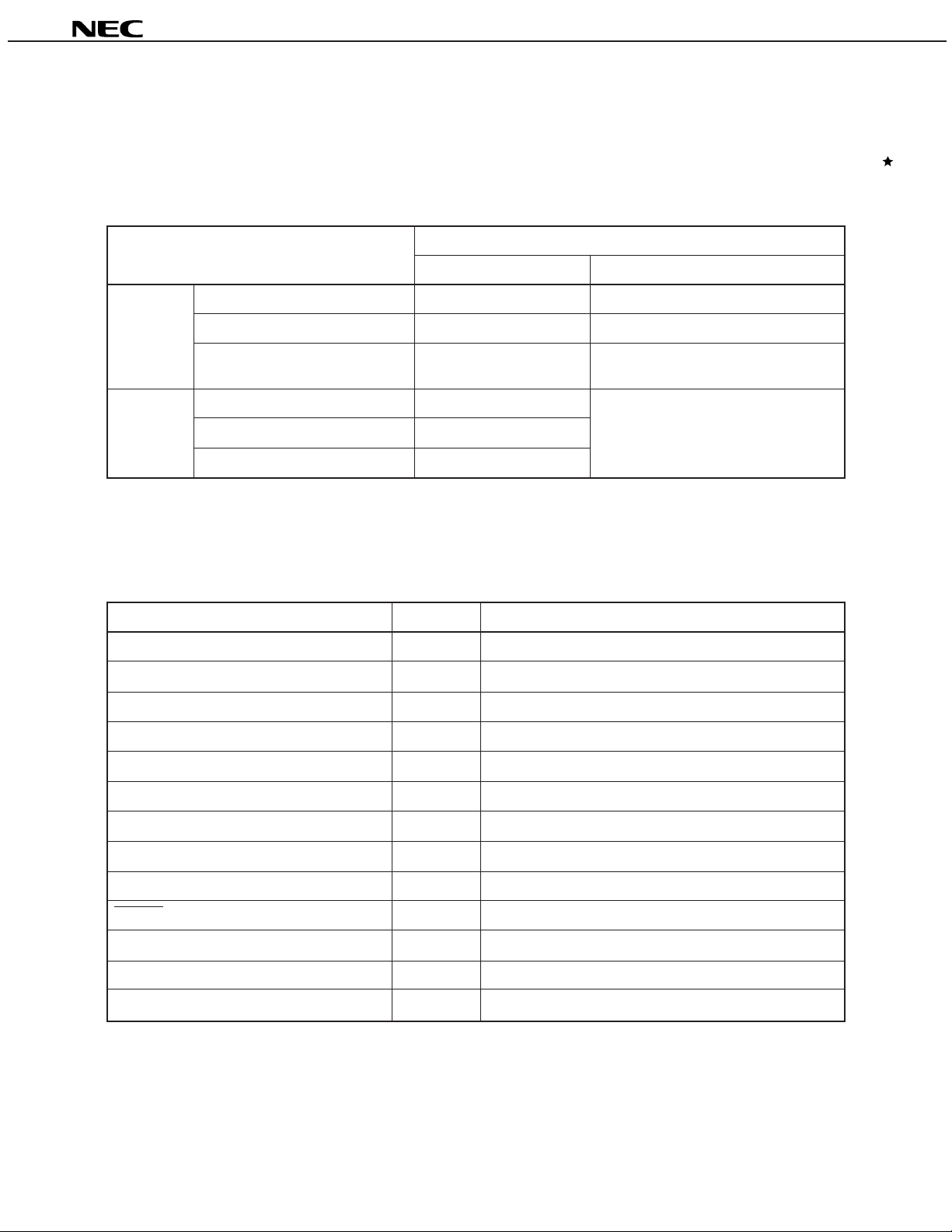
ORDERING INFORMATION
PD17201A, 17207 documents.
• Internal one-time PROM: 4096 × 16 bits
• Supply voltage:
2.5 to 5.5 V (at f
2.4 to 5.5 V (at f
2.0 to 5.5 V (at fXT = 32.768 kHz, TA = –20 to +75°C)
X = 4 MHz, TA = –20 to +75°C)
X = 4 MHz, TA = –20 to +60°C)
Part Number Package
µ
PD17P207GF-001-3B9 80-pin plastic QFP (14 × 20 mm)
µ
PD17P207GF-002-3B9 80-pin plastic QFP (14 × 20 mm)
µ
PD17P207GF-003-3B9 80-pin plastic QFP (14 × 20 mm)
The features of each product is shown in the following table:
µ
When using
subclock oscillator circuit.
Pull-up resistor of RESET pin
Main clock oscillator circuit
Subclock oscillator circuit
µ
PD17P207 is different from µPD17201A, 17207 in some of the electrical characteristics, such as
supply voltage, the operating ambient temperature, and supply current. Therefore, use µPD17P207
only for the system evaluation.
PD17P207-001, be sure to connect the resonator to the main clock oscllator circuit and
µ
Item
µ
PD17P207-001
Provided
µ
PD17P207-002
Not provided
Provided
Not provided
µ
PD17P207-003
Not provided
Provided
PD17201A, 17207
On request
(mask option)
Document No. U11777EJ3V0DS00 (3rd edition)
Previous No. IC-2707A
Date Published November 1996 P
Printed in Japan
The information in this document is subject to change without notice.
The mark shows major revised points.
©
1993
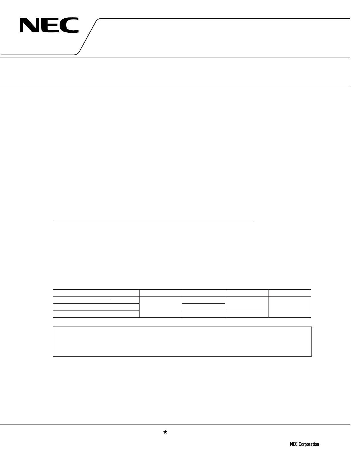
PIN CONFIGURATION (TOP VIEW)
(1) Ordinary operation mode
3
2
/COM
/COM
34
35
LCD33LCD
LCD
COM1COM0CAPL
LCD2VLCD1VLCDCVLCD0
CAPH
V
OUT
XT
XTINWDOUT
REG
V
RESET
µ
PD17P207
LCD
LCD
LCD
LCD
LCD
LCD
LCD
LCD
LCD
LCD
LCD
LCD
LCD
LCD
LCD
LCD
LCD
LCD
LCD
LCD
LCD
LCD
LCD
LCD
32
31
30
29
28
27
26
25
24
23
22
21
20
19
18
17
16
15
14
13
12
11
10
9
80 79 78 77 76 75 74 73 72 71 70 69 68 67 66 65
1
2
3
4
5
6
7
8
9
µ
PD17P207GF-3B9
10
11
12
13
14
15
16
17
18
19
20
21
22
23
24
25 26 27 28 29 30 31 32 33 34 35 36 37 38 39 40
X
64
63
62
61
60
59
58
57
56
55
54
53
52
51
50
49
48
47
46
45
44
43
42
41
OUT
X
IN
V
DD
REM
P1A
2
/SI
1
/SO
P1A
P1A
0
/SCK
P0D
3
P0D
2
P0D1/TMOUT
P0D
O
/LED
P0C
3
P0C
2
P0C
1
P0C
0
P0B
3
P0B
2
P0B
1
P0B
0
P0A
3
P0A
2
P0A
1
P0A
0
INT
8
LCD
LCD7LCD6LCD5LCD4LCD3LCD2LCD1GND
LCD0V
ADC
0
ADC
3
ADC1ADC2ADC
ADC
GND
2
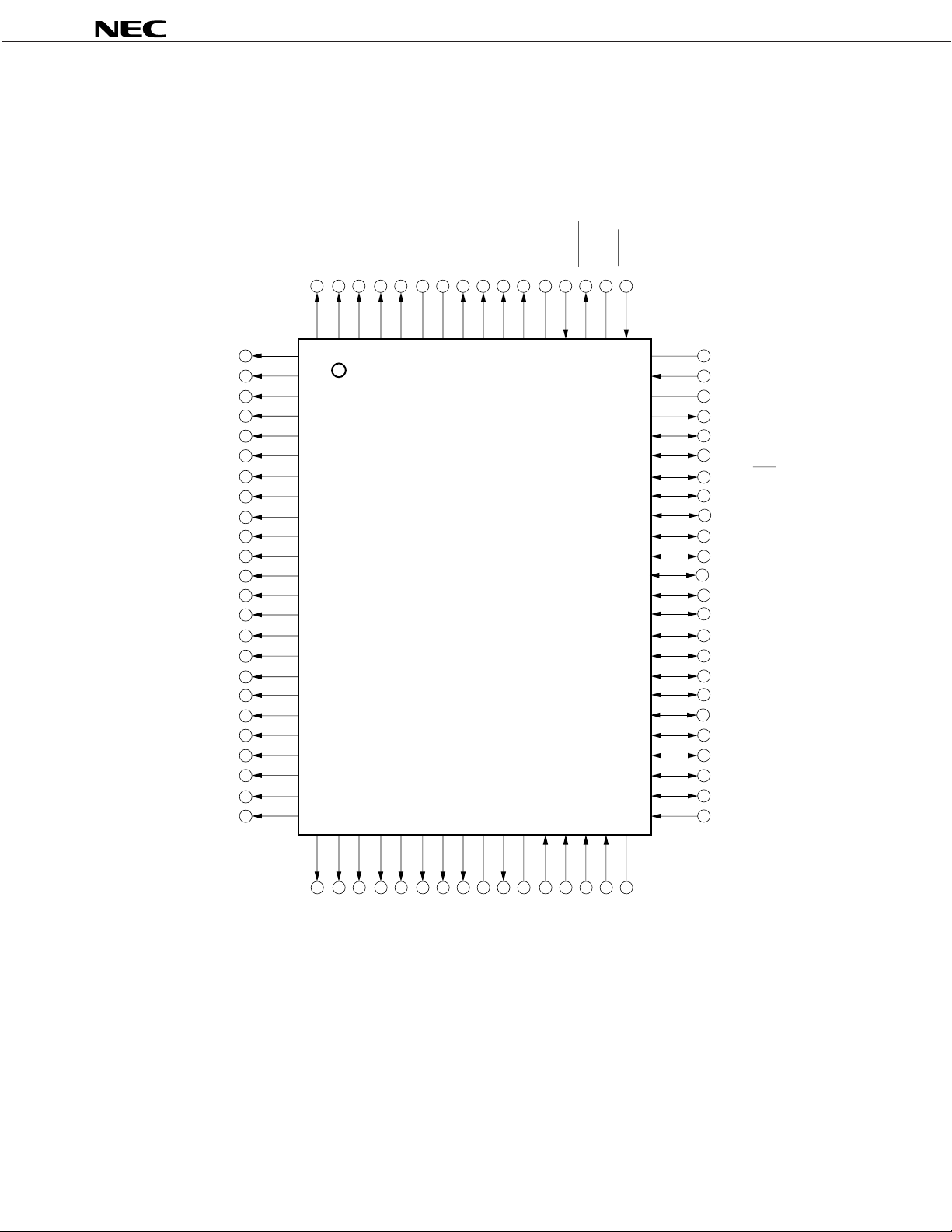
(2) PROM programming mode
µ
PD17P207
(OPEN)
(OPEN)
(L)
80 79 78 77 76 75 74 73 72 71 70 69 68 67 66 65
1
2
3
4
5
6
7
8
9
10
11
12
13
14
15
16
17
18
19
20
21
22
23
24
25 26 27 28 29 30 31 32 33 34 35 36 37 38 39 40
µ
PD17P207GF-3B9
(OPEN)
(L)
64
63
62
61
60
59
58
57
56
55
54
53
52
51
50
49
48
47
46
45
44
43
42
41
(OPEN)
CLK
DD
V
(OPEN)
(L)
7
D
6
D
5
D
4
D
3
MD
2
MD
1
MD
0
MD
3
D
2
D
1
D
0
D
V
PP
(OPEN)
GND
DD
V
(OPEN)
(L)
ADC
GND
Caution: Those enclosed in parentheses indicate the processing of the pins not used in PROM programming
mode.
L : Ground these pins through a resistor (470 Ω).
Open : Do not connect anything to these pins.
3

Pin Name
0-ADC3 : A/D converter input
ADC
CAPH, CAPL : Booster capacitor connection
CLK : PROM clock input
0-COM3 : LCD common signal output
COM
D0-D7 : PROM data I/O
GND, GNDADC : Ground
INT : External interrupt request signal input
0-LCD35 : LCD segment signal output
LCD
LED : Remote controller transfer display output
0-MD3 : PROM mode selection input
MD
P0A0-P0A3 : I/O port
P0B0-P0B3 : I/O port
0-P0C3 : I/O port
P0C
P0D0-P0D3 : I/O port
REM : Remote controller transfer output
RESET : Reset signal input
SCK : Serial clock I/O
SI : Serial data input
SO : Serial data output
TMOUT : Timer output
ADC : A/D converter power supply
V
DD : Power supply
V
VLCD0-VLCD2 : LCD drive voltage output
VLCDC : LCD drive reference voltage adjustment
PP : PROM writing power supply
V
VREG : Voltage regulator output
WDOUT : Overrun detection output
IN, XOUT : Main clock oscillator circuit
X
XTIN, XTOUT : Subclock oscillator circuit
µ
PD17P207
4
BLOCK DIAGRAM
P1A0SCK
1
/SO
P1A
2
/SI
P1A
P0A
0
(D0)
P0A1 (D1)
P0A
2
(D2)
P0A
3
(D3)
P1A
Serial
Interface
P0A
RF
RAM
336×4 bits
SYSTEM REG.
ALU
Power
Supply
Circuit
LCD
Controller
µ
PD17P207
V
REG
V
DD
CAPH
CAPL
LCD0
V
V
LCD1
V
LCD2
V
LCDC
GMD
LCD
0
LCD
1
LCD
2
LCD
3
LCD
4
LCD
33
COM3/LCD
COM2/LCD
COM
1
COM
0
34
35
P0B
P0B
P0B
P0B
P0D0/LED
P0D
0
(MD0)
1
(MD1)
2
(MD2)
3
(MD3)
P0C
0
P0C
1
P0C
2
3
P0C
1
/TMOUT
P0D
P0D
REM
(D4)
(D5)
(D6)
(D7)
P0B
Instruction
Decoder
Interrupt
Controller
One Time PROM
×
16 bits
P0C
2
3
P0D
4096
A/D
Converter
Program Counter
Stack 5×12 bits
INT (V )
pp
V
ADC
ADC
0
ADC
1
ADC
2
ADC
3
GND
ADC
RESET
WDOUT
Carrier
Generator
Timer/
Counter
Watch Timer Divider
CPU Clock Clock Stop
Main clock
IN
X (CLK)
X
OUT
CPU Clock
XT
Subclock
XT
IN
OUT
Remark Inside the parenthesis indicates pin names in the PROM programming mode.
5

µ
PD17P207
CONTENTS
1. PIN FUNCTIONS ................................................................................................................................. 7
1.1 ORDINARY OPERATION MODE .............................................................................................................. 7
1.2 PROM PROGRAMMING MODE ................................................................................................................ 9
1.3 EQUIVALENT CIRCUITS OF PINS ......................................................................................................... 10
1.4 PROCESSING OF UNUSED PINS .......................................................................................................... 11
1.5 NOTES ON USING RESET AND INT PINS (ONLY IN ORDINARY OPERATION MODE) ................... 12
2. ONE-TIME PROM (PROGRAM MEMORY) WRITING, READING, AND VERIFICATION ...............13
2.1 OPERATION MODE FOR WRITING, READING, AND VERIFICATION OF PROGRAM MEMORY ..... 13
2.2 PROGRAM MEMORY WRITE PROCEDURE ......................................................................................... 14
2.3 PROGRAM MEMORY READ PROCEDURE........................................................................................... 15
3. DEFFERENCES BETWEEN µPD17P207 AND µPD17201A/17207................................................. 16
4. ELECTRICAL CHARACTERISTICS ................................................................................................. 17
5. PACKAGE DRAWINGS .....................................................................................................................25
6. RECOMMENDED SOLDERING CONDITIONS ................................................................................ 26
APPENDIX A. MICROCONTROLLER FAMILY FOR HIGH-FUNCTION REMOTE CONTROLLER
WITH LCD ........................................................................................................................27
APPENDIX B. DEVELOPMENT TOOLS ................................................................................................ 28
6
µ
PD17P207
1. PIN FUNCTIONS
1.1 ORDINARY OPERATION MODE
Pin No. Symbol Function Output Type On Reset
76 COM0
77 COM1
78 LCD35/COM2
79 LCD34/COM3 CMOS,
80 LCD33 push-pull
1 LCD32
||
32 LCD1
34 LCD0
33 GND ––
35 VADC ––
36 ADC0
|| ––
39 ADC3
40 GNDADC ––
41 INT
42 P0A0 CMOS,
|| push-pull Input
45 P0A3
Common/segment signal outputs of the LCD driver. These common
and segment signal outputs are selected by LCDMD3 to LCDMD0
of the register file.
• COM0 to COM3
· Common signal outputs of the LCD driver
• LCD35 to LCD0
· Segment signal outputs of the LCD driver
Device ground
Positive power supply of the A/D converter (VADC should be equal to
VDD.)
Analog inputs of the A/D converter (8-bit resolution)
Ground of the A/D converter
External interrupt request signal (Input).
The interrupt request is generated at the rising edge of this signal.
4-bit I/O port (enabling setting of inputs or outputs in 4-bit units)
(Grouped I/O).
Each of these pins has a pull-up resistor.
–
– Input
46 P0B0 N-channel,
|| open-drain Input
49 P0B3
50 P0C0 N-channel,
|| open-drain Input
53 P0C3
54 P0D0/LED
55 P0D1/TMOUT
56 P0D2 push-pull
57 P0D3
4-bit I/O port (enabling setting of inputs or outputs in 4-bit units)
(Grouped I/O).
4-bit I/O port (enabling setting of inputs or outputs in 4-bit units)
(Grouped I/O).
Port 0D/LED output or 8-bit timer output.
P0D0 and LED outputs are switched by NRZEN of the register file.
P0D1 and 8-bit timer outputs are switched by TMOE of the register
file.
• P0D0 to P0D3
· 4-bit I/O port
· Enabling setting of inputs or outputs of each bit (Bitwise I/O)
• LED
· Outputs NRZ signal in synchronization with infrared remote
controller signal (REM)
· Outputs high level while remote controller carrier is output from
REM pin
• TMOUT
· Output of the 8-bit timer
CMOS, Input
(to be cont’d)
7
µ
PD17P207
(cont’d)
Pin No. Symbol Function Output Type On Reset
Port 1A or serial interface.
Port 1A and serial interface are switched by SIOEN of the
register file.
58 P1A0/SCK • P1A0 to P1A2
· 3-bit I/O port CMOS, Input
59 P1A1/SO · Enabling setting of inputs or outputs of 3 bits push-pull
(Grouped I/O)
60 P1A2/SI • SCK, SO, SI
· SCK: Serial clock I/O
· SO: Serial data output
· SI: Serial data input
61 REM Signal output to an infrared remote controller. CMOS, Low-level
Active-high output push-pull output
62 VDD Positive power supply. – –
63 XIN These pins are connected to a 4-MHz ceramic or crystal
64 XOUT resonator for main clock oscillation.
System reset input
65 RESET System is reset when low level is input to this pin. – Input
While this pin is low, oscillation of main clock is stopped.
Only µPD17P207-001 has internal pull-up resistor.
Output of the voltage regulator for the subclock oscillation
66 VREG circuit. – –
Connect external 0.1-µF capacitor to this pin.
Output for detection of a program overrun. N-channel, High-
67 WDOUT Outputs low level when the watchdog timer overflows or the open drain impedance
stack overflows/underflows. Use this pin after connecting to
the RESET pin.
68 XTIN These pins are connected to a 32.768-kHz crystal oscillator
– (Oscillates.)
69 XTOUT for subclock oscillation.
71 VLCDC Input to regulate the reference voltage to drive LCD. – –
70 VLCD0 Reference voltage outputs to drive LCD.
72 VLCD1 •VLCD0: Reference voltage output
73 VLCD2 •VLCD1: Doubler output (Two times the reference voltage) – –
•VLCD2: Tripler output (Three times the reference voltage)
(Oscillation
stops.)
74 CAPH These pins are connected to a capacitor to boost the
75 CAPL LCD drive voltage.
8
––
µ
PD17P207
1.2 PROM PROGRAMMING MODE
Pin No. Symbol Function Output Type On Reset
33 GND Ground – –
35 VDD Positive power supply – –
40 GNDADC ––
41 VPP Applies 12.5V as the program voltage when writing, reading, – –
42 D0
to to
45 D3
50 D4
to to
53 D7
46 MD0
to to Select operation mode for PROM programming. – Input
49 MD3
62 VDD Positive power supply – –
63 CLK Address update clock input – Input
Ground for A/D converter
Performs PROM programming with GNDADC = GND.
Positive power supply for PROM programming.
and verifying the program memory.
8-bit data I/O for PROM programming. Input
CMOS,
push-pull
Remark Pins other than the above are not used in the PROM programming mode. For the processing of
unused pins, refer to (2) PROM programming mode in PIN CONFIGURATION.
9
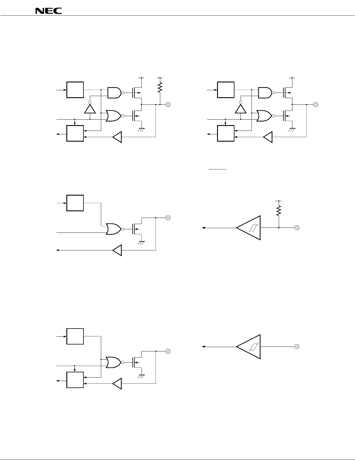
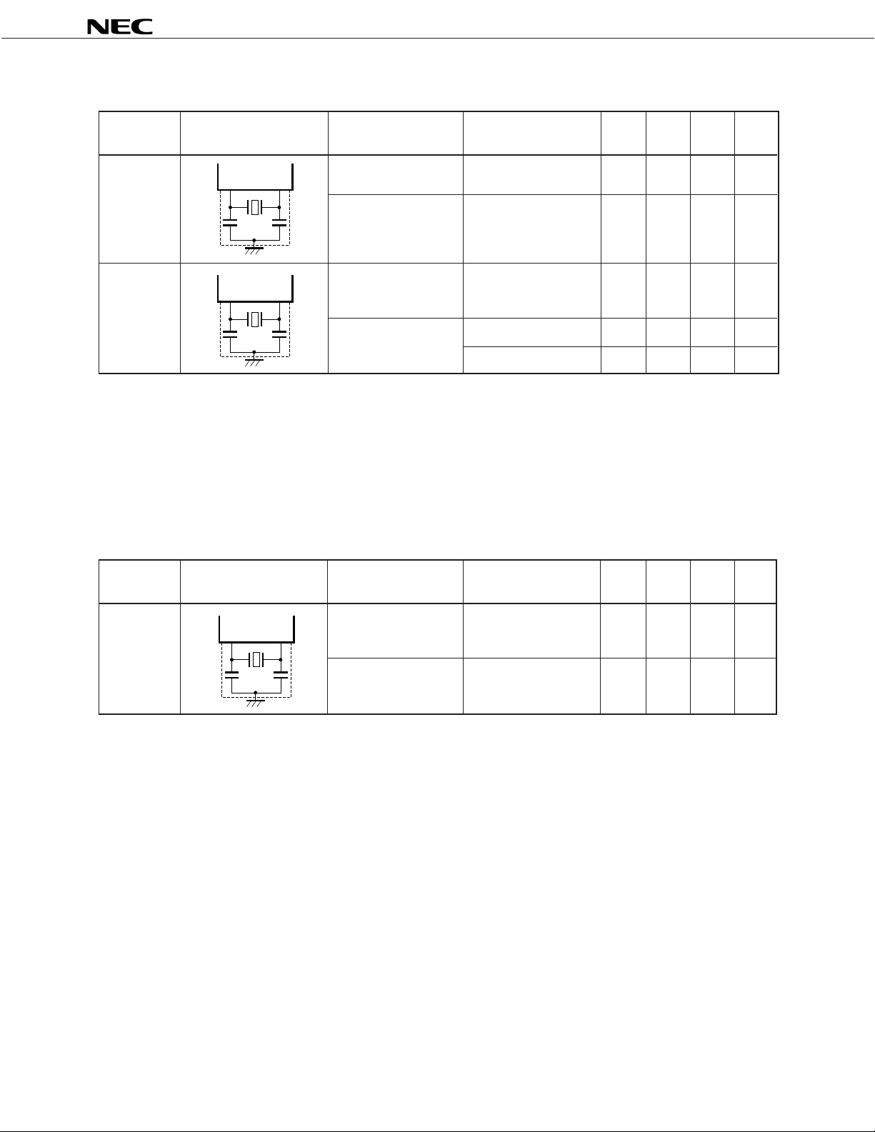
1.3 EQUIVALENT CIRCUITS OF PINS
The followings are equivalent circuits (partially simplified) of the respective pins of the µPD17P207.
(1) P0A (4) P0D, P1A
µ
PD17P207
DD
P-ch
N-ch
V
DD
data
output
disable
data
output
disable
V
Output
latch
Selector
Input buffer
(2) P0B (5) RESET
data
output
disable
Output
latch
N-ch
Output
latch
Selector
Input buffer
Input buffer
V
DD
V
DD
P-ch
N-ch
Pull-up
resistor
Note
Input buffer
(3) P0C (6) INT
data
output
disable
Output
latch
N-ch
Selector
Input buffer
Schmitt trigger input with hysteresis
characteristics
Note Only µPD17P207-001 has the internal
pull-up resistor.
Input buffer
Schmitt trigger input with hysteresis
characteristics
10
1.4 PROCESSING OF UNUSED PINS
In ordinay operation mode, process unused pins as follows:
Table 1-1. Processing of Unused Pins
(a) Port pins
µ
PD17P207
Pin Name
Input Mode P0A (Connect pull-up resistor.) Open
P0C – Directly connect to GND.
P0D, P1A – Connect each pin to VDD or GND via
Output Mode P0A (CMOS port) Outputs high level Open
P0D, P1A (CMOS port) –
P0B, P0C (N-ch open-drain port) Outputs low level
Recommended Processing of Unused Pins
Internally Externally
Note
resistor
.
Note When externally pulling a pin up (connecting the pin to VDD via resistor) and down (connecting the pin to
GND via resistor), give adequate consideration to the drive capability and current consumption of the
port. To pull a pin up or down at a high resistance, make sure that no noise is superimposed on the pin.
(b) Pins other than port pins
Pn Name I/O Mode Recommended Processing of Unused Pin
ADC0-ADC3 Input Directly connect to GND
CAPH, CAPL Output Open
COM0, COM1, COM2/LCD35, COM3/LCD34 Output Open
Note
INT
LCD0-LCD33 Output Open
REM Output Open
VADC – Directly connect to VDD
VLCD0-VLCD2 Output Open
VLCDC – Directly connect to VDD or VLCD0
WDOUT Output Directly connect to GND
XIN, XTIN Input Directly connect to GND
XOUT – Directly connect to VDD
XTOUT – Directly connect to VREG
Input Directly connect to GND
Note The INT pin is also used as a test mode setting pin. Directly connect this pin to GND when it is not used.
Cautions 1. It is recommended that the input/output mode and output level of a pin be fixed by repeatedly
setting in each loop of the program.
2. When the LCD controller/driver is not used, stop the voltage regulator by using the display mode
register.
11
µ
PD17P207
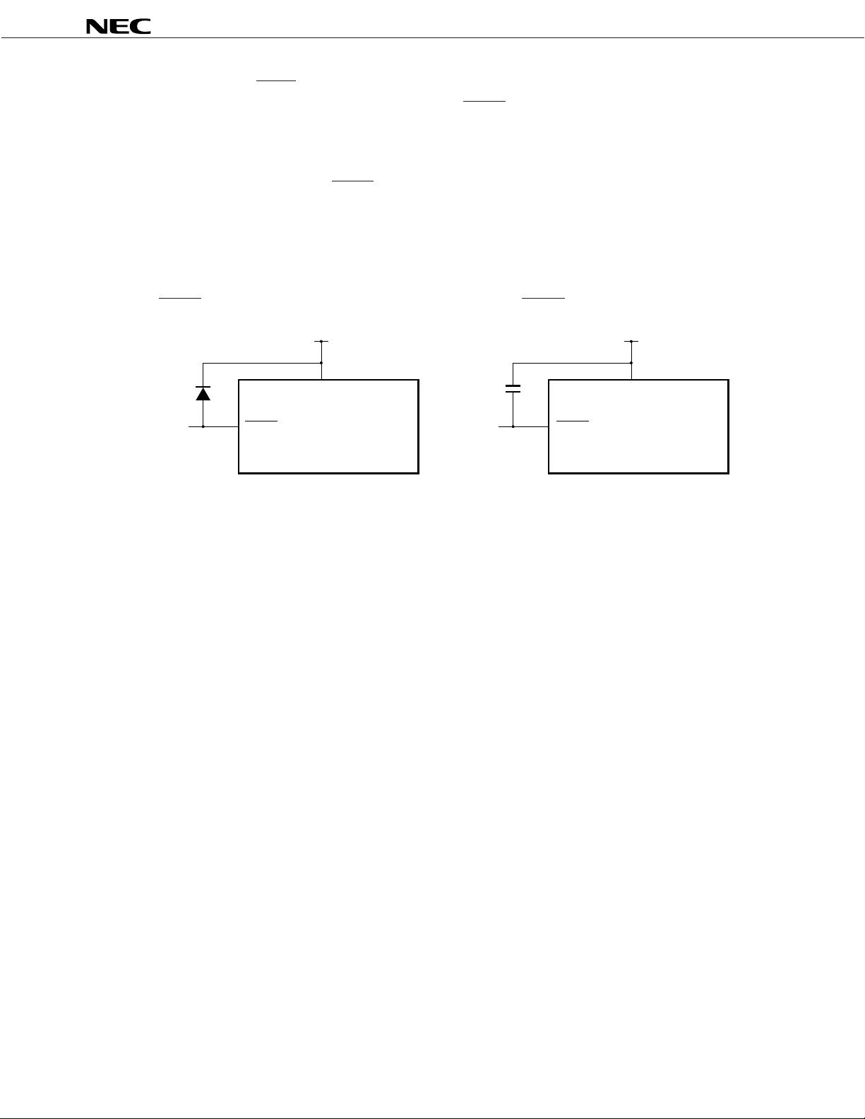
1.5 NOTES ON USING RESET AND INT PINS (ONLY IN ORDINARY OPERATION MODE)
In addition to the functions shown in 1. PIN FUNCTIONS, the RESET and INT pins also have a function to set a test
µ
mode (for IC testing) in which the internal operations of the
PD17P207are tested.
When a voltage higher than VDD is applied to either of these pins, the test mode is set. This means that, even during
ordinary operation, the µPD17P207 may be set in the test mode if a noise exceeding VDD is applied.
For example, if the wiring length of the RESET or INT pin is too long, noise superimposed on the wiring line of the pin
may cause the above problem.
Therefore, keep the wiring length of these pins as short as possible to suppress the noise; otherwise, take noise
preventive measures as shown below by using external components.
• Connect diode with low V
and RESET/INT pin
Diode with
low V
F
RESET, INT
F between VDD
V
DD
V
DD
• Connect capacitor between VDD
and RESET/INT pin
V
DD
V
DD
RESET, INT
12

µ
PD17P207
2. ONE-TIME PROM (PROGRAM MEMORY) WRITING, READING, AND VERIFICATION
µ
PD17P207 sets the PROM mode when PROM writing, reading or verification as shown in Table 2-1.
In PROM mode, no address input pin is used. Instead, the address is updated by the clock for input from the CLK pin.
Table 2-1. Pins Used for Program Memory Writing, Reading, or Verification
Pin Name
VPP
CLK
MD0-MD3
D0-D7
VDD
2.1 OPERATION MODE FOR WRITING, READING, AND VERIFICATION OF PROGRAM MEMORY
If +6 V is applied to the VDD and +12.5 V to the VPP pin after µPD17P207 has been placed in the reset status for a fixed
time (VDD = 5V, RESET = Low level), µPD17P207 enters program memory write, read, or verify mode.
The MD
Leave the pins not used for program memory writing, reading, or verification open or ground through pull-down resistors
(470 Ω). (Refer to (2) PROM programming mode in PIN CONFIGURATION.)
0 to MD3 pins are used to set the operation modes listed in Table 2-2.
Applies program voltage (12.5 V).
Inputs address update clock.
Selects operation mode.
Inputs and outputs 8-bit data.
Applies supply voltage (6 V).
Function
Table 2-2. Operating Mode for Program Memory Writing, Reading or Verification
Operating Mode Specification
PP
V
VDD
0 MD1 MD2 MD3
MD
Operating Mode
+12.5 V
Remark x: L or H
+6 V
HLHL
LHHH
LLHH
HxHH
Program memory address 0 clear mode
Write mode
Read/verify mode
Program inhibit mode
13

µ
PD17P207
2.2 PROGRAM MEMORY WRITE PROCEDURE
The program memory write procedure is as follows. High-speed program memory write is possible.
(1) Ground the unused pins through pull-down resistors. The CLK pin must be low.
(2) Supply 5 V to the V
DD pin. The VPP pin must be low.
(3) After waiting for 10 µs, supply 5 V to the VPP pin.
(4) Operate the MD0 to MD3 pins to set program memory address 0 clear mode.
(5) Supply 6 V to the V
DD pin and 12.5 V to the VPP pin.
(6) Set program inhibit mode.
(7) Write data in 1-millisecond write mode.
(8) Set program inhibit mode.
(9) Set verify mode. If data has been written connectly, proceed to step (10). If data has not yet been written,
repeat steps (7) to (9).
(10) Write additional data for (the number of times data was written (X) in steps (7) to (9)) times
1 milliseconds.
(11) Set program inhibit mode.
(12) Supply a pulse to the CLK pin four times to update the program memory address by 1.
(13) Repeat steps (7) to (12) to the last address.
(14) Set program memory address 0 clear mode.
(15) Change the voltages of V
DD and VPP pins to 5 V.
(16) Turn off the power supply.
Steps (2) to (12) are illustrated below.
Reset
Write Verify
PP
V
V
V
V
DD
DD
PP
GND
DD
+1
V
DD
V
GND
CLK
D -D
0 7
MD
0
Hi-z Hi-z Hi-z Hi-z
Data input
X-time repetition
Data
output
Additional
data write
Data input
Address
increment
14
MD
MD
MD
1
2
3

µ
PD17P207
2.3 PROGRAM MEMORY READ PROCEDURE
(1) Ground the unused pins through pull-down resistors. The CLK pin must be low.
(2) Supply 5 V to the V
DD pin. The VPP pin must be low.
(3) After waiting for 10 µs, supply 5 V to the VPP pin.
(4) Operate the MD0 to MD3 pins to set program memory address 0 clear mode.
(5) Supply 6 V to the V
DD pin and 12.5 V to the VPP pin.
(6) Set program inhibit mode.
(7) Set verify mode. Data of each address is sequentially output each time a clock pulse is input to the CLK pin
four times.
(8) Set program inhibit mode.
(9) Set program memory address 0 clear mode.
(10) Change the voltages of V
DD and VPP pins to 5 V.
(11) Turn off the power supply.
Steps (2) to (9) are illustrated below.
Reset
V
PP
V
V
PP
DD
GND
V
DD
+1
DD
V
V
DD
GND
1 cycle
CLK
D -D
0 7
MD
MD
Hi-z
0
1
“L”
Data output Data output
Hi-z
MD
MD
2
3
15
µ
PD17P207
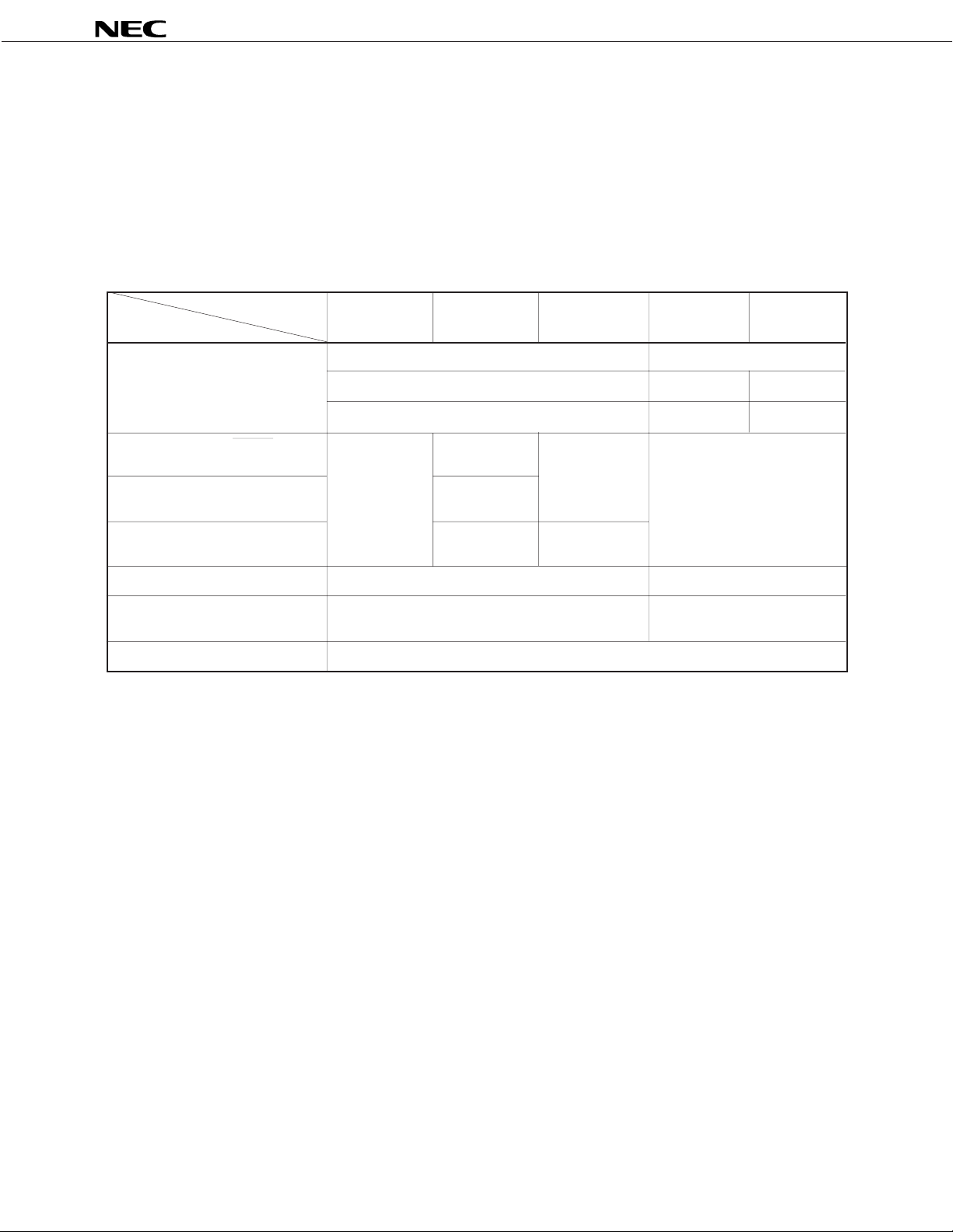
3. DIFFERENCES BETWEEN µPD17P207 AND µPD17201A/17207
The µPD17P207 has a PROM to which the user can write a program in place of the internal mask ROM (program memory)
of the µPD17201A and 17207. Therefore, the µPD17P207 is identical to µPD17201A and 17207 except for the program
memory and mask option. However, some of the electrical characteristics, such as supply current or VLCDC voltage of the
µ
PD17P207, are different from that of the µPD17201A and 17207.
The following table lists the differences between the µPD17P207 and µPD17201A/17207.
For the details of the CPU and hardware of the µPD17201A and 17207, refer to their Data Sheets.
Product Name -001 -002 -003
Item
Program Memory One-Time PROM Mask ROM
Pull-Up Resistor of RESET Pin Not
Main Clock Oscillator Circuit Provided Provided provided (mask option)
Subclock Oscillator Circuit Not Provided
VPP pin, PROM Programming Pin Provided Not provided
Supply Voltage VDD = 2.5 to 5.5 V (at fX = 4 MHz, TA = –20 to +75°C)
(TA = –20 to +75°C) VDD = 2.4 to 5.5 V (at fX = 4 MHz, TA = –20 to +60°C)
Package 80-pin plastic QFP (14 × 20 mm)
µ
PD17P207
µ
PD17P207
0000H-0FFFH 0000H-0BFFH 0000H-0FFFH
4096 × 16 bits 3072 × 16 bits 4096 × 16 bits
provided
provided
µ
PD17P207
Not Any
µ
PD17201A
VDD = 2.2 to 5.5 V (at fX = 4 MHz)
µ
PD17207
16
µ
PD17P207
4. ELECTRICAL CHARACTERISTICS
ABSOLUTE MAXIMUM RATINGS (TA = 25°C)
Parameter Symbol Conditions Rating Unit
Supply Voltage VDD –0.3 to +7.0 V
Analog Supply Voltage VADC –0.3 to +7.0 V
Input Voltage VI –0.3 to VDD+0.3 V
Output Voltage VO –0.3 to VDD+0.3 V
REM pin
High-Level One pin Peak value –7.5 mA
Output Current
Low-Level rms value 5 mA
Output Current
Operating Ambient Temperature TA –20 to +75 °C
Storage Temperature Tstg –40 to +125 °C
IOH
IOL
(except REM)
All pins Peak value –22.5 mA
(except REM)
One pin
All pins Peak value 22.5 mA
(except REM)
Peak value –30 mA
rms value –20 mA
rms value –5 mA
rms value –15 mA
Peak value 7.5 mA
rms value 15 mA
Note rms value = Peak value × √Duty
Caution Even if one of the parameters exceeds its absolute maximum rating even momentarily, the quality
of the product may be degraded. The absolute maximum rating therefore specifies the upper or lower
limit of the value at which the product can be used without physical damages. Be sure not to exceed
or fall below this value when using the product.
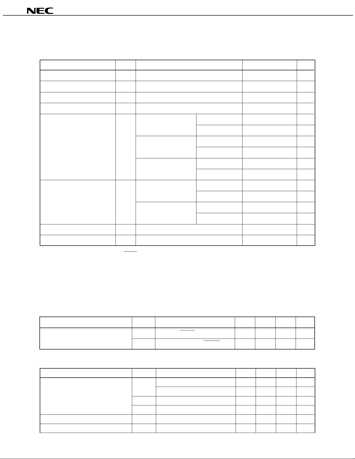
CAPACITANCE (T
Input Capacitance
A = 25°C, VDD = 0 V)
Parameter Symbol Conditions MIN. TYP. MAX. Unit
CIN1 INT and RESET pins 10 pF
CIN2 Other than INT and RESET pins 10 pF
RECOMMENDED OPERATING RANGES (TA = –20 to + 75°C)
Parameter Symbol Conditions MIN. TYP. MAX. Unit
VDD1
Supply Voltage
VDD2 System clock fX = 8 MHz 4.5 5.0 5.5 V
VDD3 System clock f XT = 32.768 kHz 2.0 3.0 5.5 V
Main Clock Oscillation Frequency fX 1.0 4.0 8.0 MHz
Subclock Oscillation Frequency fXT 32.768 kHz
System clock fX = 4 MHz 2.5 3.0 5.5 V
fX = 4 MHz, TA = –20 to + 60°C 2.4 3.0 5.5 V
17
µ
PD17P207
MAIN SYSTEM CLOCK OSCILLATOR CHARACTERISTICS (TA = –20 to +75°C, VDD = 2.5 to 5.5 V)
Resonator Item Conditions MIN. TYP. MAX. Unit
Note 3
Ceramic
Resonator
Note 3
Crystal
Resonator
Recommended
Constants
X
IN
X
OUT
X
IN
X
OUT
Oscillation 1.0 4 8.0 MHz
frequency (fX)
C2C1
C2C1
Oscillation
stabilization time minimum oscillation
Oscillation
frequency (fX)
Oscillation
stabilization time
Note 1
Note 2
Note 1
Note 2
From when VDD
reaches the 4 ms
voltage
1.0 4 8.0 MHz
VDD = 4.5 to 5.5V 10 ms
30 ms
Notes 1. The oscillation frequency is indicated only to express the oscillator characteristics. Refer to the AC
characteristics for instruction execution time.
2. The oscillation stabilization time is the time required for stabilizing the oscillation after VDD is applied
or the STOP mode is released.
3. The recommended resonators are shown in the table described later.
SUBSYSTEM CLOCK OSCILLATOR CHARACTERISTICS
Resonator Item Conditions MIN. TYP. MAX. Unit
Crystal
Resonator
Recommended
Constants
X
IN
X
OUT
Oscillation
frequency (fXT)
Oscillation
stabilization time
32.768 kHz
510s
Caution When using the main system clock and the subsystem clock generators, in order to avoid wiring
capacitance effects, the following notations must be read and observed for wiring the portion inside
the dotted line in the table:
• Wiring length must be minimized.
• Do not cross with other signal lines. Do not wire close to a large current line.
• Capacitors used in the oscillators must always be grounded to GND potential level. Never ground
the grounding pattern having a large current flow.
• Do not take the signal directly out of the oscillator.
In order to reduce the power consumption, the subsystem clock oscillator employs a low amplification factor circuit. Because of this, the subsystem clock oscillator is more sensitive to noise than
the main system clock oscillator. Therefore, when using the subsystem clock, wiring must be
carefully planned.
18

RECOMMENDED RESONATORS
Main System Clock : Ceramic Resonator
External Oscillation
Capacitance (pF) Voltage Range (V)
Manufacturer Part Name Remarks
C1 C2 MIN. MAX.
CSA3.58MG 30 30 2.0 6.0
CSA4.00MG 30 30 2.0 6.0
CSA4.19MG 30 30 2.0 6.0
µ
PD17P207
MURATA Mfg. CST3.58MGW Not Not 2.0 6.0
CST4.00MGW Not Not 2.0 6.0 Built-in capacitor
CST4.19MGW Not Not 2.0 6.0
KBR3.58MS 33 33 2.0 6.0
KYOCERA KBR4.0MS 33 33 2.0 6.0
KBR4.19MS 33 33 2.0 6.0
TOKO CRHF4.00 18 18 2.0 6.0
DAISHINKU PRS0400BCSAN 39 33 2.0 6.0
required required
required required
required required
Main System Clock : Crystal Resonator
Manufacturer Frequency Holder Capacitance (pF) Voltage Range (V) Remarks
(MHz)
KINSEKI 4.0 HC-49U-S 22 22 2.0 6.0
External Oscillation
C1 C2 MIN. MAX.
19
DC CHARACTERISTICS (TA = –20 to +75°C, VDD = VADC = 3 V)
Parameter Symbol Test Condition MIN. TYP. MAX. Unit
µ
PD17P207
High-Level Input Voltage
Low-Level Input Voltage
High-Level Input
Leakage Current
Low-Level Input
Leakage Current
High-Level Output Current
Low-Level Output Current IOL Note 2 VOL = 0.3 V 0.5 0.9 mA
Built-In Pull-Up Resistor
A/D Absolute Precision ±2 LSB
A/D Resolution 8 Bits
A/D Converter Current IADC 60 120
Consumption
VIH1 RESET and INT pins 2.4 3 V
VIH2 Other than RESET and INT pins 2.1 3 V
VIL1 RESET and INT pins 0 0.6 V
VIL2 Other than RESET and INT pins 0 0.9 V
ILIH1 XTIN, XTOUT, XIN, and XOUT pins 20
ILIH2 Other than XTIN, XTOUT, XIN, and XOUT pins 3
ILIL1 XTIN, XTOUT, XIN, and XOUT pins –20
ILIL2 Other than XTIN, XTOUT, XIN, and XOUT pins –3
IOH1 REM pin V OH = 1.8 V –7 –15 mA
IOH2 Note 1 VOH = 2.7 V –0.3 –0.7 mA
RP0A P0A0 to P0A3 pins 100 200 350 k Ω
RRES RESET pins (µPD17P207-001 only) 24 47 94 k Ω
µ
µ
µ
µ
µ
A
A
A
A
A
Comparator Error In comparator mode 10 20 mV
IDD1 X installed RUN mode 1.6 2.2 mA
IDD2 XT not installed HALT mode 1.8 mA
Supply Current IDD3 STOP mode 3.0 10.0
IDD4 X not installed or STOP RUN mode 400 600
Note 3
IDD5 (f XT = 32.768 kHz) HALT mode 20 40
(fX = 4.19 MHz)
mode XT installed
Notes 1. P0A0 to P0A3, P0D0 to P0D3, and P1A0 to P1A2 pins
2. P0A0 to P0A3, P0B0 to P0B3 , P0C0 to P0C3, P0D0 to P0D3, P1A0 to P1A2, WDOUT, and REM pins
3. The specifications of the main STOP mode (sub-mounting) are the same as the sub-HALT mode (with
the main clock oscillation stopped).
LCD CHARACTERISTICS (T
Parameter Symbol Test Condition MIN. TYP. MAX. Unit
VLCDC Output Voltage VLCDC TA = 25°C, R1 = R2 = 1 MΩ 0.5 0.65 0.8 V
LCD Reference Output Voltage VLCD0 External variable resistance 0.8 1.8 V
Doubler Output Voltage VLCD1 C1 to C4 = 0.47 µF 1.9 2.0 VLCD0
Tripler Output Voltage VLCD2 C1 to C4 = 0.47 µF 2.85 3.0 VLCD0
LCD Common Output Current ICOM Output voltage deviation = 0.2 V 30
A = –20 to +75°C, VDD = 3 V)
(0 to 2.2 MΩ)
µ
A
µ
A
µ
A
µ
A
LCD Segment Output Current ILCD Output voltage deviation = 0.2 V 5
20
µ
A
AC CHARACTERISTICS (TA = –20 to +75°C, VDD = 2.0 to 5.5 V)
Parameter Symbol Condition MIN. TYP. MAX. Unit
µ
PD17P207
VDD = 5 V±10 %
Data input 2.0
Data output 10
SCK Input Cycle Time tKCY
Data input 5
Data output 13
Data input 1.0
VDD = 5 V±10 %
SCK Input High- and tKH, Data output 5.0
Low-Level Widths
tKL Data input 2.5
Data output 6.5
SI Setup Time (Vs. SCK↑)tSIK 100 ns
SI Hold Time (Vs. SCK↑)tKSI 100 ns
SCK↓→to SO tKSO CL = 100 pF 4.5
Output Delay Time
INT High-and Low-Level Width tIOH, tIOL 50
RESET Low-Level Width tRSL 50
P0A Low-Level Width tRLSL At standby release 10
µ
µ
µ
µ
µ
µ
µ
µ
µ
µ
µ
µ
s
s
s
s
s
s
s
s
s
s
s
s
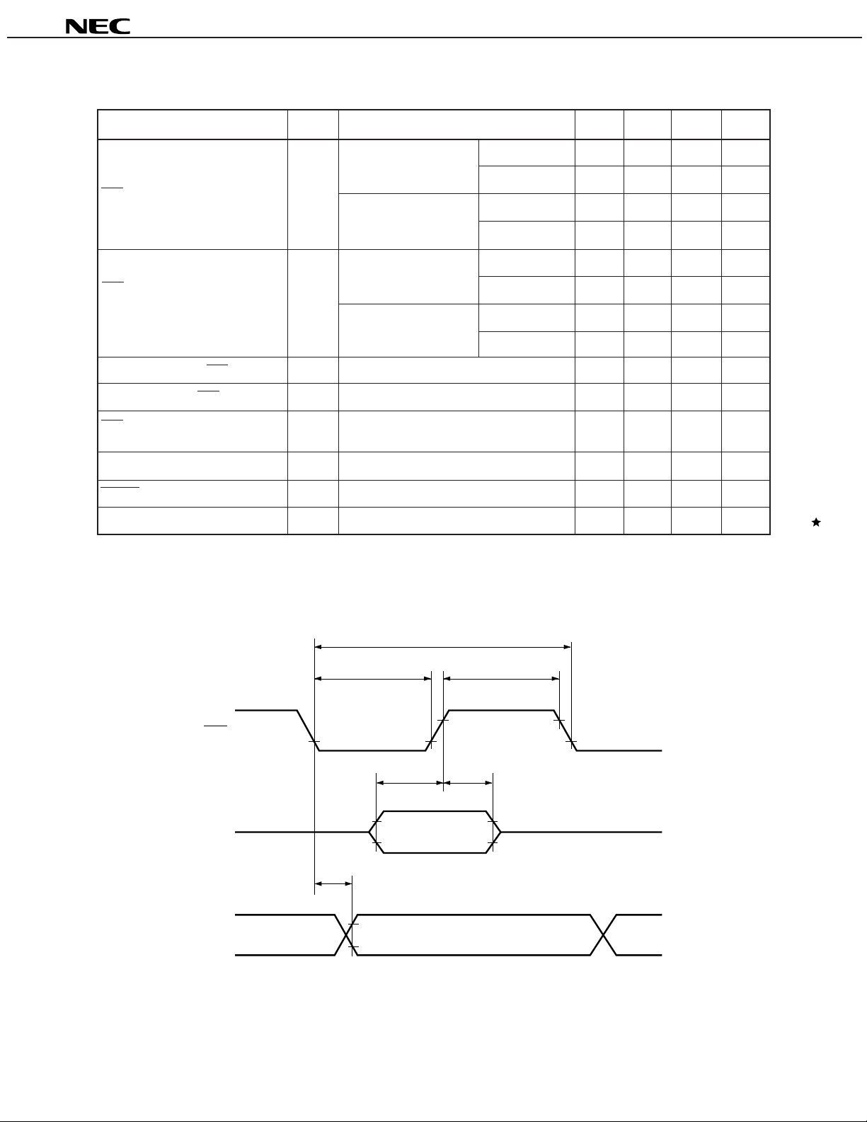
SERIAL TRANSFER TIMING
3-line Serial I/O Mode:
SCK
SI
SO
KCY
t
t
KL
t
SIK
Input data
t
KSO
Output data
t
KH
t
KSI
21

DC PROGRAMMING CHARACTERISTICS (TA = 25°C, VDD = 6.0 ±0.25V, VPP = 12.5 ±0.3V)
Parameter Symbol Conditions MIN. TYP. MAX. Unit
High-Level Input Voltage
Low-Level Input Voltage
Input Leakage Current
High-Level Output Voltage
Low-Level Output Voltage
VDD Supply Current
VPP Supply Current
VIH1
VIH2
VIL1
VIL2
ILI
VOH
VOL
IDD
IPP
Other than CLK
CLK
Other than CLK
CLK
VIN = VIL or VIH
IOH = –1 mA
IOL = 1.6 mA
MD0 = VIL, MD1 = VIH
0.7 VDD VDD V
VDD –0.5 VDD V
0 0.3 VDD V
0 0.4 V
10
VDD –1.0 V
0.4 V
30 mA
30 mA
Cautions 1. VPP must not exceed +13.5 V, including the overshoot.
2. Apply V
DD before VPP and disconnect it after VPP.
µ
PD17P207
µ
A
22

AC PROGRAMMING CHARACTERISTICS (TA = 25°C, VDD = 6.0 ±0.25V, VPP = 12.5 ±0.3V)
µ
PD17P207
Parameter
Address Setup Time
MD1 Setup Time (vs. MD0↓)
Data Setup Time (vs. MD0↓)
Address Hold Time
Data Hold Time (vs. MD0↑)
MD0 ↑→ Data Output Float Delay Time
VPP Setup Time (vs. MD3↑)
VDD Setup Time (vs. MD3↑)
Initial Program Pulse Width
Additional Program Pulse Width
MD0 Setup Time (vs. MD1↑)
MD0 ↓→ Data Output Delay Time
MD1 Hold Time (vs. MD0↑)
MD1 Recovery Time (vs. MD0↓)
Program Counter Reset Time
CLK Input High-/Low- Level Width
CLK Input Frequency
Initial Mode Set Time
MD3 Setup Time (vs. MD1↑)
MD3 Hold Time (vs. MD1↓)
MD3 Setup Time (vs. MD0↓)
Address
Address
MD3 Hold Time (vs. MD0↑)
MD3 ↓→ Data Output Float Delay Time
Reset Setup Time
Note 2
Note 2
Note 2
(vs.MD0↓)
Note 2
(vs.MD0↑)
→ Data Output Delay Time
→ Data Output Hold Time
Symbol
Note 1 Conditions MIN. TYP. MAX. Unit
tAS tAS
tM1S tOES
tDS tDS
tAH tAH
tDH tDH
tDF tDF
tVPS tVPS
tVDS tVCS
tPW tPW
tOPW tOPW
tMOS tCES
tDV tDV
tM1H tOEH
tM1R tOR
tPCR –
tXH,tXL –
fX –
tI –
tM3S –
tM3H –
tM3SR –
tDAD tACC
tHAD tOH
tM3HR –
tDFR –
tRES –
MD0 = MD1 = VIL
tM1H + tM1R ≥ 50 µs
When data is read from
program memory
2
2
2
2
2
0130
2
2
0.95 1.0 1.05 ms
0.95 21.0 ms
2
2
2
10
0.125
2
2
2
2
0130
2
10
µ
s
µ
s
µ
s
µ
s
µ
s
µ
s
µ
s
µ
s
µ
s
1
µ
s
µ
s
µ
s
µ
s
µ
s
4 MHz
µ
s
µ
s
µ
s
µ
s
2
µ
s
µ
s
µ
s
2
µ
s
µ
s
Notes 1. These symbols are the corresponding µPD27C256A (maintenance product) symbols.
2. The internal address is incremented by 1 at the third falling edge of CLK (with four clocks constituting
as one cycle). The internal address is not connected to any pin.
23

PROGRAM MEMORY WRITE TIMING
t
RES
t
PCR
t
M3S
t
VDS
VPS
Data input
DS
t
t
PW
t
M1S
ttDVt
t
M1H
V
V
PP
DD
V
V
GND
DD
+1
V
V
GND
CLK
D0 to D
MD
MD
MD
MD
PP
DD
DD
Hi-z
7
t
I
0
1
t
2
3
µ
t
XH
t
Hi-z Hi-z Hi-z Hi-z
OH
t
M1R
Data
output
t
MOS
Data input
DF
t
DS
t
OPW
XL
t
DH
t
AH
Data input
t
AS
t
M3H
PD17P207
PROGRAM MEMORY READ TIMING
t
RES
V
V
PP
V
DD
V
GND
V
DD
V
GND
CLK
D0 to D
MD
MD
MD
+1
PP
DD
DD
7
t
I
0
1
“L”
t
2
Hi-z Hi-z
PCR
t
t
VPS
t
VDS
M3SR
t
XH
t
XL
t
HAD
Data output Data output
t
DV
t
DAD
t
M3HR
t
DFR
24
MD
3

5. PACKAGE DRAWINGS
µ
PD17P207
80 PIN PLASTIC QFP (14
64
65
80
1
F
G
P
20)
A
B
41
24
40
C D
25
detail of lead end
S
Q
R
J
H
M
I
K
M
N
L
NOTE
Each lead centerline is located within 0.15 mm (0.006 inch) of
its true position (T.P.) at maximum material condition.
ITEM MILLIMETERS INCHES
A 23.2±0.2 0.913
B 20.0±0.2 0.787
C 14.0±0.2 0.551
D 17.2±0.2 0.677±0.008
F
1.0
G
1.8
H 0.35±0.10 0.014
I 0.15 0.006
J 0.8 (T.P.)
K 1.6±0.2
L 0.8±0.2 0.031
M 0.15 0.006
N 0.10 0.004
P 2.7
Q
R5°±5° 5°±5°
S
+0.10
–0.05
0.125±0.075
3.0 MAX. 0.119 MAX.
+0.009
–0.008
+0.009
–0.008
+0.009
–0.008
0.039
0.031
+0.004
–0.005
0.031 (T.P.)
0.063±0.008
+0.009
–0.008
+0.004
–0.003
0.106
0.005±0.003
S80GF-80-3B9-3
25

µ
PD17P207
6. RECOMMENDED SOLDERING CONDITIONS
When mounting the µPD17P207 by soldering, soldering should be performed under the following recommended
contitions.
For details on recommended soldering conditions, refer to the information document “Semconductor Device
Mounting Technology Manual” (C10535E).
For other soldering methods, please cousult with NEC sales personnel.
Table 6-1. Conditions for Surface Mounting
µ
PD17P207GF-001-3B9 : 80-pin plastic QFP ( 14 × 20 mm)
µ
PD17P207GF-002-3B9 : 80-pin plastic QFP ( 14 × 20 mm)
µ
PD17P207GF-003-3B9 : 80-pin plastic QFP ( 14 × 20 mm)
Soldering Method Soldering Conditions Conditions
Package peak temperature: 235°C,
Infrared Reflow Number of times: 2 max., Number of days: 7
VPS Number of times: 2 max., Number of days: 7
Wave Soldering Soldering bath temperature: 260 °C max., Time: 10 seconds max., WS 60-207-1
Partial Heating Pin temperature: 300°C max., Time: 3 seconds max. (per device)
Time: 30 seconds max. (210°C min.),
necessary at 125 °C for 20 hours)
<Precaution>
Products other than those supplied in thermal-resistant tray (magazine,
taping, and non-thermal-resistant tray) cannot be baked in their packs.
Package peak temperature: 215°C
Time: 40 seconds max. (200°C min.),
necessary at 125 °C for 20 hours)
<Precaution>
Products other than those supplied in thermal-resistant tray (magazine,
taping, and non-thermal-resistant tray) cannot be baked in their packs.
Number of times: 1
Preheating temperature: 120 °C max. (package surface temperature)
Number of days: 7
20 hours)
Note
(after that, prebaking is necessary at 125 °C for
Note
(after that, prebaking is IR35-207-2
Note
(after that, prebaking is VP15-207-2
Recommended
Reference Code
Note Number of days after unpacking the dry pack. Storage conditions are 25°C and 65 %RH max.
Caution Do not use different soldering methods together (however, pin partial heating can be performed with
other soldering methods).
26

µ
PD17P207
APPENDIX A. MICROCONTROLLER FAMILY FOR HIGH-FUNCTION REMOTE CONTROLLER
WITH LCD
µ
Product Name
Item
PD17201A
µ
PD17207
µ
PD17P207
ROM Capacity 3072 × 16 bits 4096 × 16 bits 4096 × 16 bits
RAM Capacity 336 × 4 bits
LCD Controller/Driver 136 segments max.
Infrared Remote Controller LED output is high-active.
Carrier Generator
Number of I/O Ports 19
External Interrupt (INT) 1
Timer 8-bit timer : 1
Watchdog Timer Internal (WDOUT output)
Serial Interface 1 channel
Stack 5 levels (3 levels for multiplexed interrupt)
Main
Instruction
Execution
Time
Supply
Voltage
(TA = –20 to
+75°C)
System 4 µs (4 MHz: with ceramic or crystal oscillator)
Clock
Subsystem 488 µs (32.768 kHz: with crystal osciallator)
Clock
Main 2.5 to 5.5 V
System 2.2 to 5.5 V
Clock 2.4 to 5.5 V
Subsystem 2.0 to 5.5 V
Clock
(Mask ROM) (Mask ROM) (One-Time PROM)
2 channels
Watch timer: 1
Note
Standby Function STOP, HALT
Pakcage 80-pin plastic QFP
Note TA = –20 to + 60°C
27

APPENDIX B. DEVELOPMENT TOOLS
To develop the programs for the µPD17P207, the following development tools are available:
Hardware
Name Remarks
µ
PD17P207
In-Circuit Emulator
IE-17K
IE-17K-ET
EMU-17K
SE Board This is an SE board for µPD17201A, 17207, and 17P207. It can be used alone to evaluate
(SE-17207) a system or in combination with an in-circuit emulator for debugging.
Emulation Probe EP-17201GF is an emulation probe for µPD17201A, 17207, and 17P207. When used with
(EP-17201GF) EV-9200G-80, it connects an SE board to the target system.
Conversion Socket EV-9200G-80 is a conversion socket for 80-pin QFP (14 × 20 mm) and is used to connect
(EV-9200G-80
PROM Programmer AF-9703, AF-9704, AF-9705, and AF-9706 are PROM programmers corresponding to
(AF-9703
AF-9704
AF-9705
AF-9706
Program Adapter AF-9808A is an adapter that is used to program µPD17P207, and is used in combination
(AF-9808
Note 1
Note 2
Note 3
) EP-17201GF to the target system.
Note 4,
Note 4
,
Note 4
,
Note 4
)
Note 4
) with AF-9703, AF-9704, AF-9705, or AF-9706.
IE-17K, IE-17K-ET, and EMU-17K are the in-circuit emulators used in common with the
17K series microcomputer.
IE-17K and IE-17K-ET are connected to a PC-9800 series or IBM PC/ATTM as the host
machine with RS-232C. EMU-17K is inserted into the expansion slot of a PC-9800 series.
By using these in-circuit emulators with a system evaluation board corresponding to the
microcomputer, the emulators can emulate the microcomputer. A higher level
debugging environment can be provided by using man-machine interface
SIMPLEHOST
EMU-17K also has a function by which you can check the contents of data memory realtime.
µ
PD17P207. By connecting program adapter AF-9808A to this PROM programmer,
µ
PD17P207 can be programmed.
TM
.
Notes 1. Low-cost model: External power supply type
2. This is a product from IC Corp. For details, consult IC Corp.
3. Two EV-9200G-80s are supplied with the EP-17201GF. Five EV-9200G-80s are optionally available as
a set.
4. These are products from Ando Electric. For details, consult Ando Electric.
28

Software
µ
PD17P207
Name
17K Series
Assembler
(AS17K)
Device File
AS17201
AS17207
Support
Software
(
SIMPLE-
HOST
)
Outline
AS17K is an assembler that
can be used in common with
the 17K series products. When
developing the program of the
µ
PD17P207, AS17K is used in
combination with a device file
(AS17201 or AS17207).
AS17201 is a device file for
µ
PD17201A.
AS17207 is a device file for
µ
PD17207.
These are used in combination
with an assembler for the 17K
series (AS17K).
SIMPLEHOST
package that enables manmachine interface on the
WindowsTM when a program is
developed by using an in-circuit
emulator and a personal
computer.
is a software
Host
Machine
PC-9800
series
IBM PC/AT
PC-9800
series
IBM PC/AT
PC-9800
series
IBM PC/AT
MS-DOS
PC DOS
MS-DOS
PC DOS
OS Media
MS-DOS
PC DOS
Windows
TM
TM
Supply
5" 2HD
3.5" 2HD
5" 2HC
3.5" 2HC
5" 2HD
3.5" 2HD
5" 2HC
3.5" 2HC
5" 2HD
3.5" 2HD
5" 2HC
3.5" 2HC
Order Code
µ
S5A10AS17K
µ
S5A13AS17K
µ
S7B10AS17K
µ
S7B13AS17K
µ
S5A10AS17201
µ
S5A10AS17207
µ
S5A13AS17201
µ
S5A13AS17207
µ
S7B10AS17201
µ
S7B10AS17207
µ
S7B13AS17201
µ
S7B13AS17207
µ
S5A10IE17K
µ
S5A13IE17K
µ
S7B10IE17K
µ
S7B13IE17K
Remark The corresponding OS versions are as follows:
OS Version
MS-DOS Ver. 3.30 to Ver. 5.00A
PC DOS Ver. 3.1 to Ver. 5.0
Windows Ver. 3.0 to Ver. 3.1
Note
Note
Note Ver. 5.00/5.00A of MS-DOS and
Ver. 5.0 of PC DOS have a task
swap function, but this function
cannot be used with this software.
29

NOTES FOR CMOS DEVICES
1 PRECAUTION AGAINST ESD FOR SEMICONDUCTORS
Note: Strong electric field, when exposed to a MOS device, can cause destruction of
the gate oxide and ultimately degrade the device operation. Steps must be taken
to stop generation of static electricity as much as possible, and quickly dissipate
it once, when it has occurred. Environmental control must be adequate. When
it is dry, humidifier should be used. It is recommended to avoid using insulators
that easily build static electricity. Semiconductor devices must be stored and
transported in an anti-static container, static shielding bag or conductive
material. All test and measurement tools including work bench and floor should
be grounded. The operator should be grounded using wrist strap. Semiconduc-
tor devices must not be touched with bare hands. Similar precautions need to
be taken for PW boards with semiconductor devices on it.
µ
PD17P207
2 HANDLING OF UNUSED INPUT PINS FOR CMOS
Note: No connection for CMOS device inputs can be cause of malfunction. If no
connection is provided to the input pins, it is possible that an internal input level
may be generated due to noise, etc., hence causing malfunction. CMOS device
behave differently than Bipolar or NMOS devices. Input levels of CMOS devices
must be fixed high or low by using a pull-up or pull-down circuitry. Each unused
pin should be connected to VDD or GND with a resistor, if it is considered to have
a possibility of being an output pin. All handling related to the unused pins must
be judged device by device and related specifications governing the devices.
3 STATUS BEFORE INITIALIZATION OF MOS DEVICES
Note: Power-on does not necessarily define initial status of MOS device. Production
process of MOS does not define the initial operation status of the device.
Immediately after the power source is turned ON, the devices with reset function
have not yet been initialized. Hence, power-on does not guarantee out-pin
levels, I/O settings or contents of registers. Device is not initialized until the
reset signal is received. Reset operation must be executed immediately after
power-on for devices having reset function.
30

µ
PD17P207
Regional Information
Some information contained in this document may vary from country to country. Before using any NEC
product in your application, please contact the NEC office in your country to obtain a list of authorized
representatives and distributors. They will verify:
• Device availability
• Ordering information
• Product release schedule
• Availability of related technical literature
• Development environment specifications (for example, specifications for third-party tools and
components, host computers, power plugs, AC supply voltages, and so forth)
• Network requirements
In addition, trademarks, registered trademarks, export restrictions, and other legal issues may also vary
from country to country.
NEC Electronics Inc. (U.S.)
Santa Clara, California
Tel: 800-366-9782
Fax: 800-729-9288
NEC Electronics (Germany) GmbH
Duesseldorf, Germany
Tel: 0211-65 03 02
Fax: 0211-65 03 490
NEC Electronics (Germany) GmbH
Benelux Office
Eindhoven, The Netherlands
Tel:040-2445845
Fax: 040-2444580
NEC Electronics (France) S.A.
Velizy-Villacoublay, France
Tel:01-30-67 58 00
Fax: 01-30-67 58 99
NEC Electronics Hong Kong Ltd.
Hong Kong
Tel:2886-9318
Fax: 2886-9022/9044
NEC Electronics Hong Kong Ltd.
Seoul Branch
Seoul, Korea
Tel: 02-528-0303
Fax: 02-528-4411
NEC Electronics (UK) Ltd.
Milton Keynes, UK
Tel: 01908-691-133
Fax: 01908-670-290
NEC Electronics Italiana s.r.1.
Milano, Italy
Tel: 02-66 75 41
Fax: 02-66 75 42 99
NEC Electronics (France) S.A.
Spain Office
Madrid, Spain
Tel: 01-504-2787
Fax: 01-504-2860
NEC Electronics (Germany) GmbH
Scandinavia Office
Taeby, Sweden
Tel: 08-63 80 820
Fax: 08-63 80 388
NEC Electronics Singapore Pte. Ltd.
United Square, Singapore 1130
Tel:253-8311
Fax: 250-3583
NEC Electronics Taiwan Ltd.
Taipei, Taiwan
Tel: 02-719-2377
Fax: 02-719-5951
NEC do Brasil S.A.
Sao Paulo-SP, Brasil
Tel: 011-889-1680
Fax: 011-889-1689
J96. 8
31

[MEMO]
µ
PD17P207
SIMPLEHOST
MS-DOS and Windows are trademarks of Microsoft Corporation.
PC/AT and PC DOS are trademarks of IBM Corporation.
The export of this product from Japan is regulated by the Japanese government. To export this product may be prohibited
without governmental license, the need for which must be judged by the customer. The export or re-export of this product
from a country other than Japan may also be prohibited without a license from that country. Please call an NEC sales
representative.
No part of this document may be copied or reproduced in any form or by any means without the prior written
consent of NEC Corporation. NEC Corporation assumes no responsibility for any errors which may appear in
this document.
NEC Corporation does not assume any liability for infringement of patents, copyrights or other intellectual property
rights of third parties by or arising from use of a device described herein or any other liability arising from use
of such device. No license, either express, implied or otherwise, is granted under any patents, copyrights or other
intellectual property rights of NEC Corporation or others.
While NEC Corporation has been making continuous effort to enhance the reliability of its semiconductor devices,
the possibility of defects cannot be eliminated entirely. To minimize risks of damage or injury to persons or
property arising from a defect in an NEC semiconductor device, customers must incorporate sufficient safety
measures in its design, such as redundancy, fire-containment, and anti-failure features.
NEC devices are classified into the following three quality grades:
"Standard", "Special", and "Specific". The Specific quality grade applies only to devices developed based on a
customer designated "quality assurance program" for a specific application. The recommended applications of
a device depend on its quality grade, as indicated below. Customers must check the quality grade of each device
before using it in a particular application.
Standard: Computers, office equipment, communications equipment, test and measurement equipment,
audio and visual equipment, home electronic appliances, machine tools, personal electronic
equipment and industrial robots
Special: Transportation equipment (automobiles, trains, ships, etc.), traffic control systems, anti-disaster
systems, anti-crime systems, safety equipment and medical equipment (not specifically designed
for life support)
Specific: Aircrafts, aerospace equipment, submersible repeaters, nuclear reactor control systems, life
support systems or medical equipment for life support, etc.
The quality grade of NEC devices is "Standard" unless otherwise specified in NEC's Data Sheets or Data Books.
If customers intend to use NEC devices for applications other than those specified for Standard quality grade,
they should contact an NEC sales representative in advance.
Anti-radioactive design is not implemented in this product.
is a trademark of NEC Corporation.
M4 96.5
 Loading...