
DATA SHEET
MOS INTEGRATED CIRCUIT
µ
PD178P018
8-BIT SINGLE-CHIP MICROCONTROLLER
DESCRIPTION
The µPD178P018 is a device in which the on-chip mask ROM of the µPD178018 is replaced with a one-time
PROM or EPROM.
Because this device can be programmed by users, it is ideally suited for system evaluation, small-lot and multiple-
device production, and early development and time-to-market.
The µPD178P018 is a PROM version corresponding to the µPD178004, 178006, and 178016.
µ
Caution The
PD178P018KK-T does not maintain planned reliability when used in your system’s massproduced products. Please use only experimentally or for evaluation purposes during trial manufacture.
For more information on functions, refer to the following User’s Manuals. Be sure to read them when
designing.
µ
PD178018 Subseries User’s Manual: U11410E
78K/0 Series User’s Manual Instruction: U12326E (In Preparation)
FEATURES
• Pin-compatible with mask ROM version (except for VPP pin)
• Internal PROM: 60 Kbytes
•µPD178P018GC : One-time programmable (ideally suited for small-lot production)
•
µ
PD178P018KK-T : Reprogrammable (ideally suited for system evaluation)
• Internal high-speed RAM: 1024 bytes
• Internal expansion RAM: 2048 bytes
• Buffer RAM: 32 bytes
• Can be operated in the same power supply voltage as the mask ROM version
(During PLL operation: V
The electrical specifications (power supply current, etc.) and PLL analog specifications of the
differ from that of mask ROM versions. So, these differences should be considered and verified before
application sets are mass-produced.
DD = 4.5 to 5.5 V)
µ
PD178P018
In this document, the term PROM is used in parts common to one-time PROM versions and EPROM versions.
The information in this document is subject to change without notice.
Document No. U12298EJ1V0DS00 (1st Edition)
Date Published May 1997 N
Printed in Japan
©
1997
APPLICATIONS
Car stereo, home stereo systems
ORDERING INFORMATION
Part Number Package Internal ROM Quality Grade
µ
PD178P018GC-3B9 80-pin plastic QFP (14 × 14 mm, 0.65-mm pitch) One-Time PROM Standard
µ
PD178P018KK-T
Note
80-pin ceramic WQFN (14 × 14 mm, 0.65-mm pitch) EPROM Not applicable
Note Under planning
Please refer to "Quality grade on NEC Semiconductor Devices" (Document number C11531E) published by
NEC Corporation to know the specification of quality grade on the devices and its recommended applications.
µ
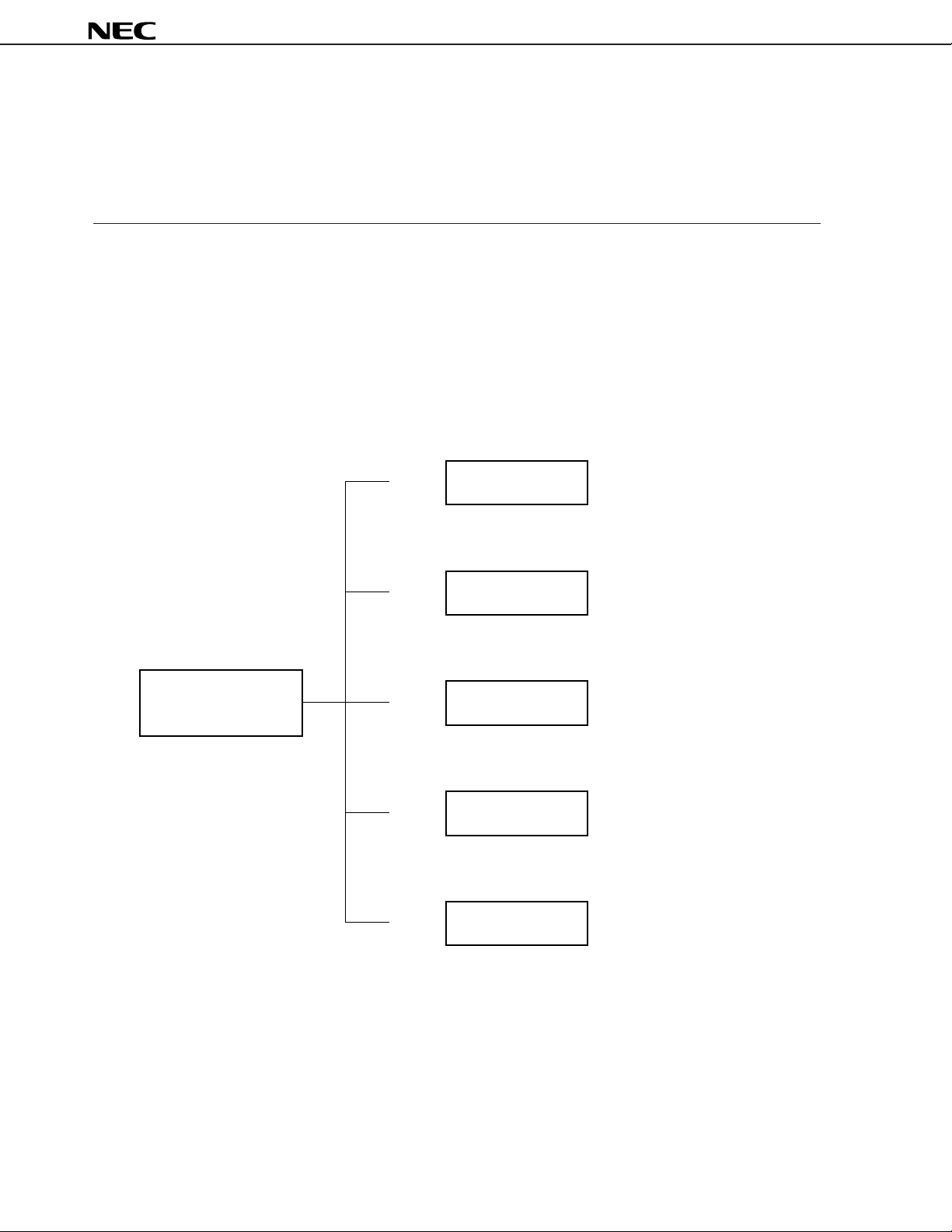
PD178018 SUBSERIES EXPANSION
PD178P018
80 pins PROM: 60 KB RAM: 3 KB
µ
µ
PD178P018
PD178018 Subseries
µ
80 pins ROM: 60 KB RAM: 3 KBPD178018
80 pins ROM: 48 KB RAM: 3 KB
80 pins ROM: 48 KB RAM: 1 KB
80 pins ROM: 32 KB RAM: 1 KB
µ
PD178016
µ
PD178006
µ
µ
PD178004
2

µ
PD178P018
FUNCTION DESCRIPTION
Item Function
Internal memory • PROM : 60 Kbytes
• RAM
High-speed RAM : 1024 bytes
Expansion RAM : 2048 bytes
Buffer RAM : 32 bytes
General register 8 bits × 32 registers (8 bits × 8 registers × 4 banks)
Instruction cycle With variable instruction execution time function
0.44 µs/0.88 µs/1.78 µs/3.56 µs/7.11 µs/14.22 µs (with 4.5-MHz crystal resonator)
Instruction set • 16-bit operation
• Multiply/divide (8 bits × 8 bits, 16 bits ÷ 8 bits)
• Bit manipulate (set, reset, test, Boolean operation)
• BCD Adjust, etc.
I/O port Total : 62 pins
• CMOS input : 1 pin
• CMOS I/O : 54 pins
• N-ch open-drain I/O : 4 pins
• N-ch open-drain output : 3 pins
A/D converter 8-bit resolution × 6 channels
Serial interface • 3-wire/SBI/2-wire/I2C bus
• 3-wire serial I/O mode
(with automatic transmit/receive function of up to 32 bytes): 1 channel
Timer • Basic timer (timer carry FF (10 Hz)) : 1 channel
• 8-bit timer/event counter : 2 channels
• 8-bit timer (D/A converter: PWM output): 1 channel
• Watchdog timer : 1 channel
Buzzer (BEEP) output 1.5 kHz, 3 kHz, 6 kHz
Vectored Maskable interrupt Internal: 8, external: 7
interrupt Non-maskable interrupt Internal: 1
Software interrupt Internal: 1
Test input Internal: 1
PLL frequency Division mode Two types
synthesizer • Direct division mode (VCOL pin)
• Pulse swallow mode (VCOH and VCOL pins)
Reference frequency 11 types selectable by program (1, 1.25, 2.5, 3, 5, 6.25, 9, 10, 12.5, 25, 50 kHz)
Charge pump Error out output: 2
Phase comparator Unlock detectable by program
Frequency counter • Frequency measurement
• AMIFC pin: for 450-kHz count
• FMIFC pin: for 450-kHz/10.7-MHz count
D/A converter (PWM output) 8-/9-bit resolution × 3 channels (shared by 8-bit timer)
Standby function • HALT mode
• STOP mode
Note
mode selectable : 1 channel
(1/2)
Note When using the I2C bus mode (including when this mode is implemented by program without using the
peripheral hardware), consult your local NEC sales representative when you place an order for mask.
3

µ
PD178P018
Item Function
Reset • Reset via the RESET pin
• Internal reset by watchdog timer
• Reset by power-ON clear circuit (3-value detection)
• Detection of less than 4.5 V
• Detection of less than 3.5 V
• Detection of less than 2.5 V
Power supply voltage • VDD = 4.5 to 5.5 V (with PLL operating)
•VDD = 3.5 to 5.5 V (with CPU operating, CPU clock: fX/2 or less)
•VDD = 4.5 to 5.5 V (with CPU operating, CPU clock: fX)
Package • 80-pin plastic QFP (14 × 14 mm, 0.65-mm pitch)
• 80-pin ceramic WQFN (14 × 14 mm, 0.65-mm pitch)
Note
(CPU clock: fX)
Note
(CPU clock: fX/2 or less and on power application)
Note
(in STOP mode)
Note These voltage values are maximum values. The reset is actually executed at a voltage lower than these
values.
(2/2)
4
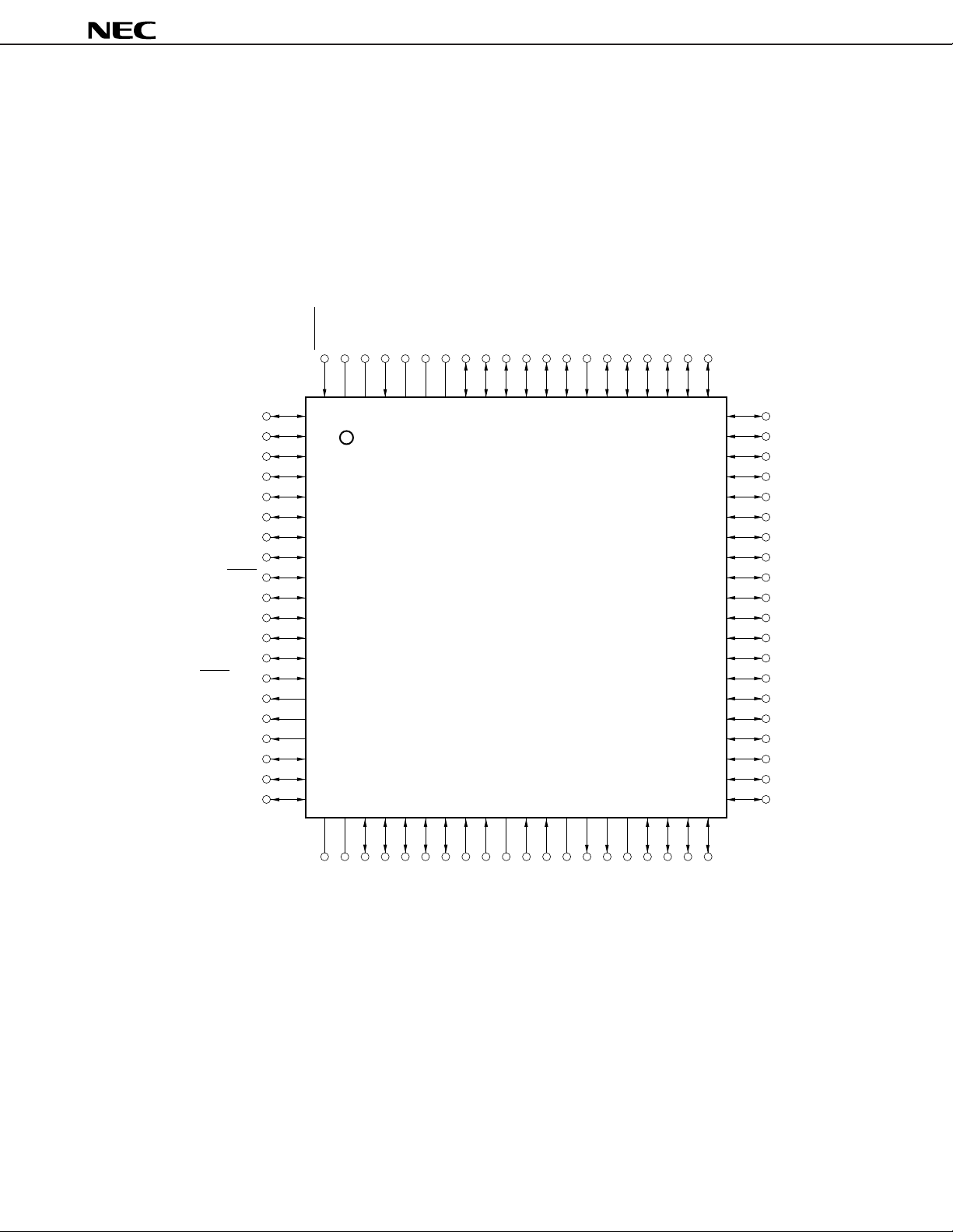
PIN CONFIGURATIONS (TOP VIEW)
(1) Normal operating mode
• 80-PIN PLASTIC QFP (14 × 14 mm, 0.65-mm pitch)
µ
PD178P018GC-3B9
• 80-PIN CERAMIC WQFN (14 × 14 mm, 0.65-mm pitch)
µ
PD178P018KK-T
RESET
P10/ANI0
P11/ANI1
P12/ANI2
P13/ANI3
P14/ANI4
P15/ANI5
P20/SI1
P21/SO1
P22/SCK1
P23/STB
P24/BUSY
P25/SI0/SB0/SDA0
P26/SO0/SB1/SDA1
P27/SCK0/SCL
P132/PWM0
P133/PWM1
P134/PWM2
P40
P41
P42
VDDREGOSCX1X2
80 79 78 77 76 75 74 73 72 71 70 69 68 67 66 65 64 63 62 61
1
2
3
4
5
6
7
8
9
10
11
12
13
14
15
16
17
18
19
20
2122 23 24 25 26 27 28 29 30 31 32 33 34 35 36 37 38 39 40
GND
REGCPU
P06/INTP6
P05/INTP5
P04/INTP4
P03/INTP3
P02/INTP2
P01/INTP1
P00/INTP0
P125
P124
P123
P122
P121
µ
PD178P018
P120
60
59
58
57
56
55
54
53
52
51
50
49
48
47
46
45
44
43
42
41
P37
P36/BEEP
P35
P34/TI2
P33/TI1
P32
P31
P30
P67
P66
P65
P64
P63
P62
P61
P60
P57
P56
P55
P54
GNDPORT
Cautions 1. Connect the V
2. Connect the VDDPORT and VDDPLL pins to VDD.
3. Connect the GNDPORT and GNDPLL pins to GND.
4. Connect each of the REGOSC and REGCPU pins to GND via a 0.1-µF capacitor.
P43
P44
P45
P46
P47
DDPORT
V
PP pin to GND directly.
AMIFC
DDPLL
FMIFC
V
VCOL
VCOH
EO0
GNDPLL
EO1
PP
V
P50
P51
P52
P53
5

µ
PD178P018
AMIFC : AM Intermediate Frequency Counter Input
ANI0 to ANI5 : A/D Converter Input
BEEP : Buzzer Output
BUSY : Busy Output
EO0, EO1 : Error Out Output
FMIFC : FM Intermediate Frequency Counter Input
GND : Ground
GNDPLL : PLL Ground
GNDPORT : Port Ground
INTP0 to INTP6 : Interrupt Inputs
P00 to P06 : Port 0
P10 to P15 : Port 1
P20 to P27 : Port 2
P30 to P37 : Port 3
P40 to P47 : Port 4
P50 to P57 : Port 5
P60 to P67 : Port 6
P120 to P125 : Port 12
P132 to P134 : Port 13
PWM0 to PWM2 : PWM Output
REGCPU : Regulator for CPU Power Supply
REGOSC : Regulator for Oscillator
RESET : Reset Input
SB0, SB1 : Serial Data Bus Input/Output
SCK0, SCK1 : Serial Clock Input/Output
SCL : Serial Clock Input/Output
SDA0, SDA1 : Serial Data Input/Output
SI0, SI1 : Serial Data Input
SO0, SO1 : Serial Data Output
STB : Strobe Output
TI1, TI2 : Timer Clock Input
VCOL, VCOH : Local Oscillation Input
DD : Power Supply
V
V
DDPLL : PLL Power Supply
DDPORT : Port Power Supply
V
V
PP : Programming Power Supply
X1, X2 : Crystal Resonator Connection
6
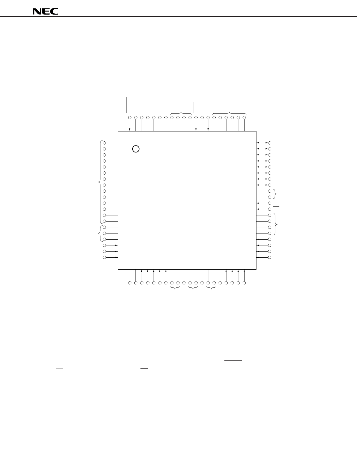
(2) PROM programming mode
µ
PD178P018
• 80-PIN PLASTIC QFP (14 ×
µ
PD178P018GC-3B9
• 80-PIN CERAMIC WQFN
(L)
A0
A1
A2
Note
1
2
3
4
5
6
7
8
9
10
11
12
13
14
15
16
17
18
19
20
µ
PD178P018KK-T
Open
14 mm)
(L)
RESET
VDDVDD(L)
80 79 78 77767574 73 72717069 68 67 66656463 62 61
21 22 23 24252627 28 29303132 33 34 35363738 39 40
Open
GND
DD
V
PGM
(L)
A9
(L)
60
59
58
57
56
55
54
53
52
51
50
49
48
47
46
45
44
43
42
41
D7
D6
D5
D4
D3
D2
D1
D0
(L)
CE
OE
(L)
A15
A14
A13
A12
Open
PP
A8
V
A16
A10
A11
DD
A3A4A5A6A7
V
GND
(L)
DD
V
(L)
GND
Note Under planning
Cautions 1. (L) : Individually connect to GND via a pull-down resistor.
2. GND : Connect to GND.
3. RESET : Set to the low level.
4. Open : Leave open.
A0 to A16 : Address Bus
CE : Chip Enable
D0 to D7 : Data Bus
GND : Ground
OE : Output Enable
PGM : Program
RESET : Reset
V
DD : Power Supply
PP : Programming Power Supply
V
7
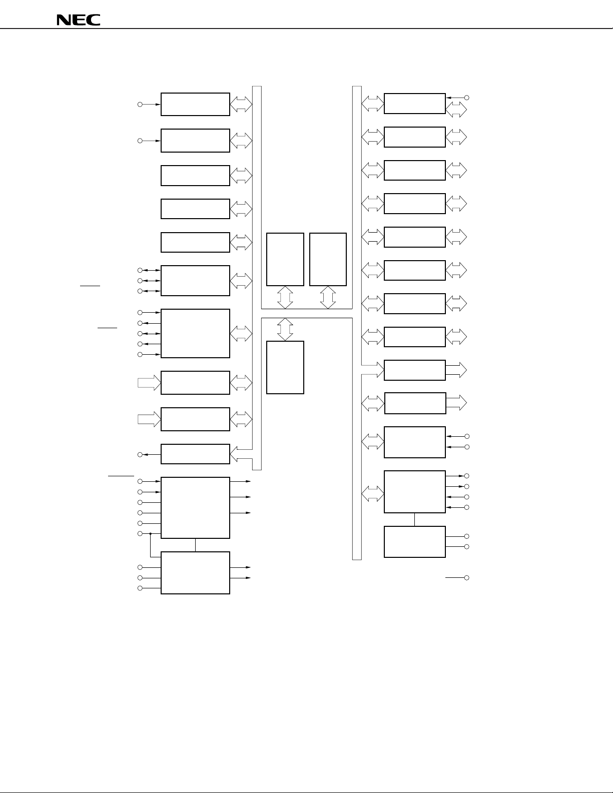
BLOCK DIAGRAM
µ
PD178P018
TI1/P33
TI2/P34
SI0/SB0/SDA0/P25
SO0/SB1/SDA1/P26
SCK0/SCL/P27
SI1/P20
SO1/P21
SCK1/P22
STB/P23
BUSY/P24
ANI0/P10 to
ANI5/P15
INTP0/P00 to
INTP6/P06
BEEP/P36
8-bit TIMER/
EVENT COUNTER 1
8-bit TIMER/
EVENT COUNTER 2
8-bit TIMER3
WATCHDOG TIMER
BASIC TIMER
SERIAL
INTERFACE 0
SERIAL
INTERFACE 1
A/D CONVERTER
6
INTERRUPT
7
CONTROL
BUZZER OUTPUT
78K/0
CPU
CORE
RAM
(3072 Bytes)
PROM
(60 K Bytes)
PORT 0
PORT 1
PORT 2
PORT 3
PORT 4
PORT 5
PORT 6
PORT 12
PORT 13
D/A CONVERTER
(PWM)
FREQUENCY
COUNTER
P00
6
P01 to P06
6
P10 to P15
P20 to P27
8
8
P30 to P37
8
P40 to P47
8
P50 to P57
8
P60 to P67
6
P120 to P125
3
P132 to P134
PWM0/P132 to
3
PWM2/P134
AMIFC
FMIFC
RESET
V
DD
X1
X2
PORT
SYSTEM
CONTROL
RESET
CPU
PERIPHERAL
PLL
EO0
EO1
VCOL
VCOH
GNDPORT
V
REGOSC
REGCPU
DD
V
VOLTAGE
REGULATOR
OSC
V
CPU
PLL
VOLTAGE
REGULATOR
V
DD
PLL
GNDPLL
PP
V
GND
8

µ
PD178P018
CONTENTS
1. PIN FUNCTION LIST.......................................................................................................................... 10
1.1 Pins in Normal Operating Mode ............................................................................................... 10
1.2 Pins in PROM Programming Mode........................................................................................... 12
1.3 Pins Input/Output Circuits and Recommended Connection of Unused Pins ...................... 13
2. PROM PROGRAMMING ..................................................................................................................... 16
2.1 Operating Modes........................................................................................................................ 16
2.2 PROM Write Procedure ............................................................................................................. 18
2.3 PROM Read Procedure.............................................................................................................. 22
3. PROGRAM ERASURE (µPD178P018KK-T ONLY) ....................................................................... 23
4. OPAQUE FILM ON ERASURE WINDOW (µPD178P018KK-T ONLY)........................................ 23
5. ONE-TIME PROM VERSION SCREENING .................................................................................... 23
6. ELECTRICAL SPECIFICATIONS ...................................................................................................... 24
7. PACKAGE DRAWINGS ..................................................................................................................... 46
8. RECOMMENDED SOLDERING CONDITIONS ................................................................................. 48
APPENDIX A. DEVELOPMENT TOOLS ................................................................................................ 49
APPENDIX B. RELATED DOCUMENTS ................................................................................................ 53
9

1. PIN FUNCTION LIST
1.1 Pins in Normal Operating Mode
(1) Port pins
µ
PD178P018
Pin Name I/O Function After Reset
P00 Input Port 0. Input only Input INTP0
P01 to P06 I/O 7-bit input/output port.
P10 to P15 I/O Port 1. Input ANI0 to ANI5
6-bit input/output port.
Input/output mode can be specified bit-wise.
P20 I/O Port 2. Input SI1
P21 8-bit input/output port. SO1
P22 Input/output mode can be specified bit-wise. SCK1
P23 STB
P24 BUSY
P25 SI0/SB0/SDA0
P26
P27 SCK0/SCL
P30 to P32 I/O Port 3. Input —
P33 8-bit input/output port. TI1
P34 Input/output mode can be specified bit-wise. TI2
P35 —
P36 BEEP
P37 —
P40 to P47 I/O Port 4. Input —
8-bit input/output port.
Input/output mode can be specified in 8-bit units.
Test input flag (KRIF) is set to 1 by falling edge detection.
P50 to P57 I/O Port 5. Input —
8-bit input/output port.
Input/output mode can be specified bit-wise.
P60 to P63 I/O Port 6. Middle voltage N-ch open-drain Input —
8-bit input/output port. input/output port.
P64 to P67 Input/output mode can be LEDs can be driven directly.
specified bit-wise.
P120 to I/O Port 12. Input —
P125 6-bit input/output port.
Input/output mode can be specified bit-wise.
P132 to Output Port 13. — PWM0 to
P134 3-bit output port. PWM2
N-ch open-drain output port.
Input/output mode can be specified bit-wise.
Input INTP1 to INTP6
Alternate Function
SO0/SB1/SDA1
10

(2) Non-port pins (1 of 2)
µ
PD178P018
Pin Name I/O Function After Reset
INTP0 to Input External maskable interrupt inputs with specifiable valid edges (rising Input P00 to P06
INTP6 edge, falling edge, both rising and falling edges).
SI0 Input Serial interface serial data input Input
SI1 P20
SO0 Output Serial interface serial data output Input
SO1 P21
SB0 I/O Serial interface serial data input/output Input P25/SI0/SDA0
SB1
SDA0 P25/SI0/SB0
SDA1 P26/SO0/SB1
SCK0 I/O Serial interface serial clock input/output Input P27/SCL
SCK1 P22
SCL P27/SCK0
STB Output Serial interface automatic transmit/receive strobe output Input P23
BUSY Input Serial interface automatic transmit busy input Input P24
TI1 Input External count clock input to 8-bit timer (TM1) Input P33
TI2 External count clock input to 8-bit timer (TM2) P34
BEEP Output Buzzer output Input P36
ANI0 to ANI5
PWM0 to Output PWM output — P132 to P134
PWM2
EO0, EO1 Output Error out output from charge pump of the PLL frequency synthesizer — —
VCOL Input Inputs PLL local band oscillation frequency (In HF, MF mode). — —
VCOH Input Inputs PLL local band oscillation frequency (In VHF mode). — —
AMIFC Input Inputs AM intermediate frequency counter. — —
FMIFC Input Inputs FM intermediate frequency counter. — —
RESET Input System reset input — —
X1 Input Crystal resonator connection for system clock oscillation — —
X2 — ——
REGOSC — Regulator for oscillator. Connected to GND via a 0.1-µF capacitor. — —
REGCPU — Regulator for CPU power supply. Connected to GND via a 0.1-µF capacitor. — —
VDD — Positive power supply — —
GND — Ground ——
VDDPORT — Positive power supply for port block — —
GNDPORT — Ground for port block — —
VDDPLL — Positive power supply for PLL — —
GNDPLL — Ground for PLL — —
Input A/D converter analog input Input P10 to P15
Alternate Function
P25/SB0/SDA0
P26/SB1/SDA1
P26/SO0/SDA1
11

(2) Non-port pins (2/2)
µ
PD178P018
Pin Name I/O Function After Reset
VPP — High-voltage applied during program write/verification. — —
Connected directly to GND in normal operating mode.
Alternate Function
1.2 Pins in PROM Programming Mode
Pin Name I/O Function
RESET Input PROM programming mode setting
When +5 V or +12.5 V is applied to VPP pin and a low-level signal is applied to the RESET pin, this
chip is set in the PROM programming mode.
VPP Input PROM programming mode setting and high-voltage applied during program write/verification.
A0 to A16 Input Address bus
D0 to D7 I/O Data bus
CE Input PROM enable input/program pulse input
OE Input Read strobe input to PROM
PGM Input Program/program inhibit input in PROM programming mode.
VDD — Positive power supply
GND — Ground potential
12

µ
PD178P018
1.3 Pins Input/Output Circuits and Recommended Connection of Unused Pins
Table 1-1 shows the input/output circuit types of pins and the recommended conditions for unused pins.
Refer to Figure 1-1 for the configuration of the input/output circuit of each type.
Table 1-1. Type of I/O Circuit of Each Pin
Pin Name I/O Circuit Type I/O Recommended Connections of Unused Pins
P00/INTP0 2 Input Connected to GND or GNDPORT
P01/INTP1 to P06/INTP6 8 I/O Set in general-purpose input port mode by software and
P10/ANI0 to P15/ANI5 11-A individually connected to VDD, VDDPORT, GND, or GNDPORT
P20/SI1 8 via a resistor.
P21/SO1 5
P22/SCK1 8
P23/STB 5
P24/BUSY 8
P25/SI0/SB0/SDA0 10
P26/SO0/SB1/SDA1
P27/SCK0/SCL
P30 to P32 5
P33/TI1, P34/TI2 8
P35 5
P36/BEEP
P37
P40 to P47 5-G
P50 to P57 5
P60 to P63 13
P64 to P67 5
P120 to P125
P132/PWM0 to P134/PWM2 19 Output Set to the low-level output by software and open
EO0 DTS-EO1 Open
EO1 DTS-EO2
VCOL, VCOH DTS-AMP Input Set to disabled status by software and open
AMIFC, FMIFC
VPP — — Connected to GND or GNDPORT directly
13
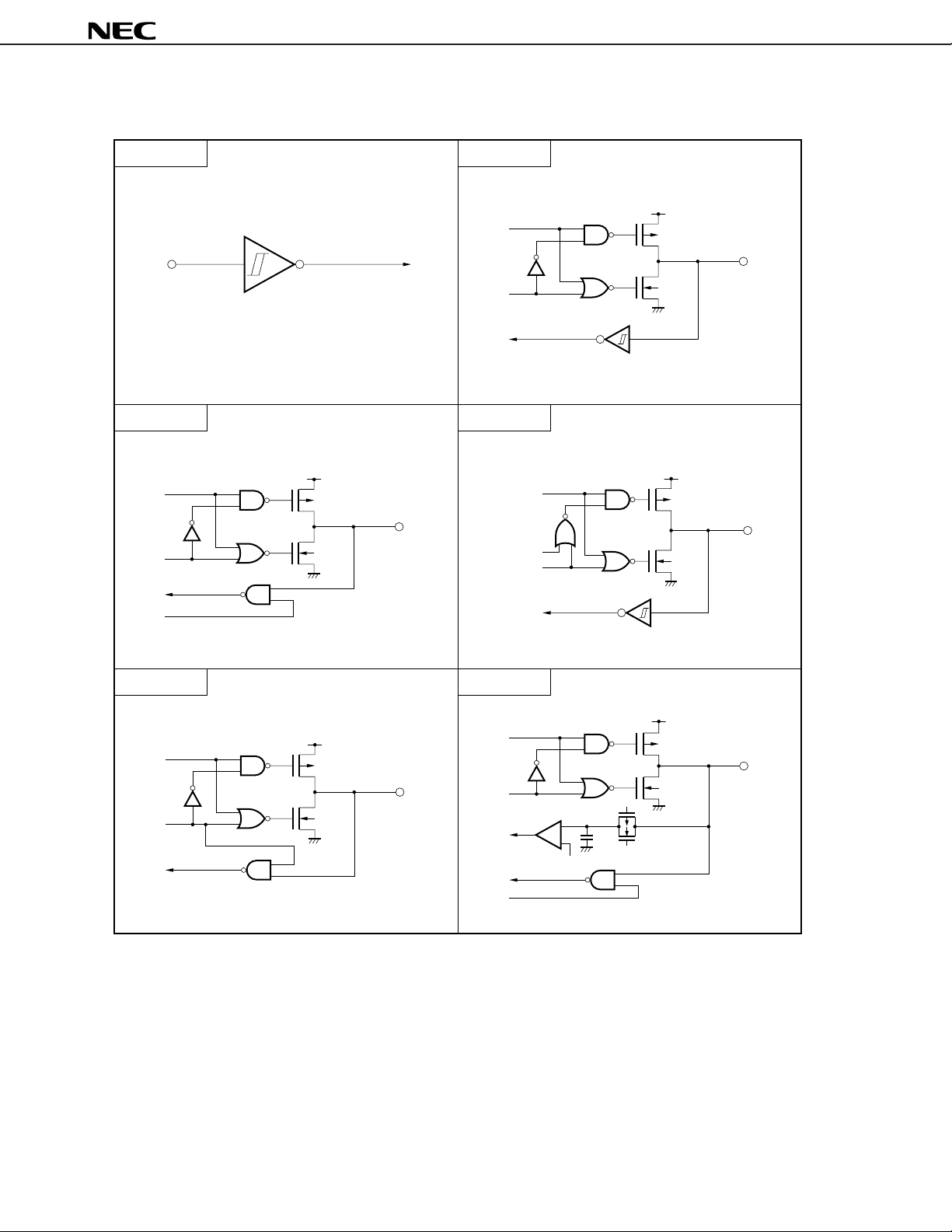
Figure 1-1. Types of Pin Input/Output Circuits (1/2)
Type 2 Type 8
data
IN
output
disable
Schmitt-Triggered Input with Hysteresis Characteristics
V
DD
P-ch
N-ch
µ
PD178P018
IN/OUT
Type 5
data
V
DD
P-ch
Type 10
IN/OUT
output
disable
N-ch
open drain
output disable
input
enable
Type 5-G Type 11-A
V
data
output
disable
DD
P-ch
IN/OUT
N-ch
data
output
disable
comparator
input
enable
data
P-ch
+
–
N-ch
V
REF
(Threshold voltage)
V
DD
P-ch
N-ch
V
P-ch
N-ch
IN/OUT
DD
IN/OUT
Remark All V
14
DD and GND in the above figures are the positive power supply and ground potential of the ports,
and should be read as V
DDPORT and GNDPORT, respectively.
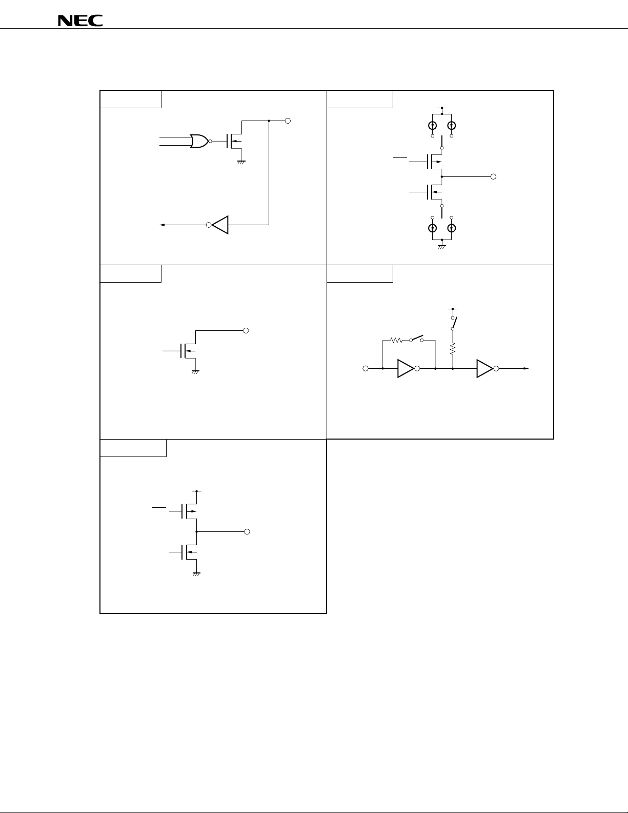
Figure 1-1. Types of Pin Input/Output Circuits (2/2)
µ
PD178P018
Type 13 Type DTS-EO2
IN/OUT
output disable
data
Middle-Voltage Input Buffer
Type 19
N-ch
N-ch
Type DTS-AMP
OUT
IN
DW
UP
DD
V
P-ch
N-ch
GNDPLL
V
PLL
DD
OUT
PLL
Type DTS-EO1
DW
Remark All V
and should be read as V
DD
PLL
V
P-ch
OUT
UP
DD and GND in the above figures are the positive power supply and ground potential of the ports,
N-ch
GNDPLL
DDPORT and GNDPORT, respectively.
15

µ
PD178P018
2. PROM PROGRAMMING
The µPD178P018 has an internal 60-Kbyte PROM as a program memory. For programming, set the PROM
programming mode with the V
PP and RESET pins. For the connection of unused pins, refer to “PIN CONFIGURA-
TIONS (TOP VIEW) (2) PROM programming mode.”
Caution Programs must be written in addresses 0000H to EFFFH (the last address EFFFH must be
specified). They cannot be written by a PROM writer which cannot specify the write address.
2.1 Operating Modes
When +5 V or +12.5 V is applied to the V
PP pin and a low-level signal is applied to the RESET pin, the PROM
programming mode is set. This mode will become the operating mode as shown in Table 2-1 when the CE, OE, and
PGM pins are set as shown.
Further, when the read mode is set, it is possible to read the contents of the PROM.
Table 2-1. Operating Modes of PROM Programming
Pin RESET VPP VDD CE OE PGM D0 to D7
Operating Mode
Page data latch L +12.5 V +6.5 V H L H Data input
Page write H H L High-impedance
Byte write L H L Data input
Program verify L L H Data output
Program inhibit x H H High-impedance
xLL
Read +5 V +5 V L L H Data output
Output disable L H x High-impedance
Standby H x x High-impedance
Remark x : L or H
16

µ
PD178P018
(1) Read mode
Read mode is set if CE = L and OE = L are set.
(2) Output disable mode
Data output becomes high-impedance, and is in the output disable mode, if OE = H is set.
µ
Therefore, it allows data to be read from any device by controlling the OE pin, if multiple
connected to the data bus.
(3) Standby mode
Standby mode is set if CE = H is set.
In this mode, data outputs become high-impedance irrespective of the OE status.
(4) Page data latch mode
Page data latch mode is set if CE = H, PGM = H, and OE = L are set at the beginning of page write mode.
In this mode, 1 page 4-byte data is latched in an internal address/data latch circuit.
(5) Page write mode
After 1 page 4 bytes of addresses and data are latched in the page data latch mode, a page write is executed
by applying a 0.1-ms program pulse (active low) to the PGM pin with CE = H and OE = H. Then, program
verification can be performed, if CE = L and OE = L are set.
If programming is not performed by a one-time program pulse, X times (X ≤ 10) write and verification operations
should be executed repeatedly.
PD178P018s are
(6) Byte write mode
Byte write is executed when a 0.1-ms program pulse (active low) is applied to the PGM pin with CE = L and OE
= H. Then, program verification can be performed if OE = L is set.
If programming is not performed by a one-time program pulse, X times (X ≤ 10) write and verification operations
should be executed repeatedly.
(7) Program verify mode
Program verify mode is set if CE = L, PGM = H, and OE = L are set.
In this mode, check if a write operation is performed correctly after the write.
(8) Program inhibit mode
Program inhibit mode is used when the OE pin, V
in parallel and a write is performed to one of those devices.
When a write operation is performed, the page write mode or byte write mode described above is used. At this
time, a write is not performed to a device which has the PGM pin driven high.
PP pin, and D0 to D7 pins of multiple
µ
PD178P018s are connected
17
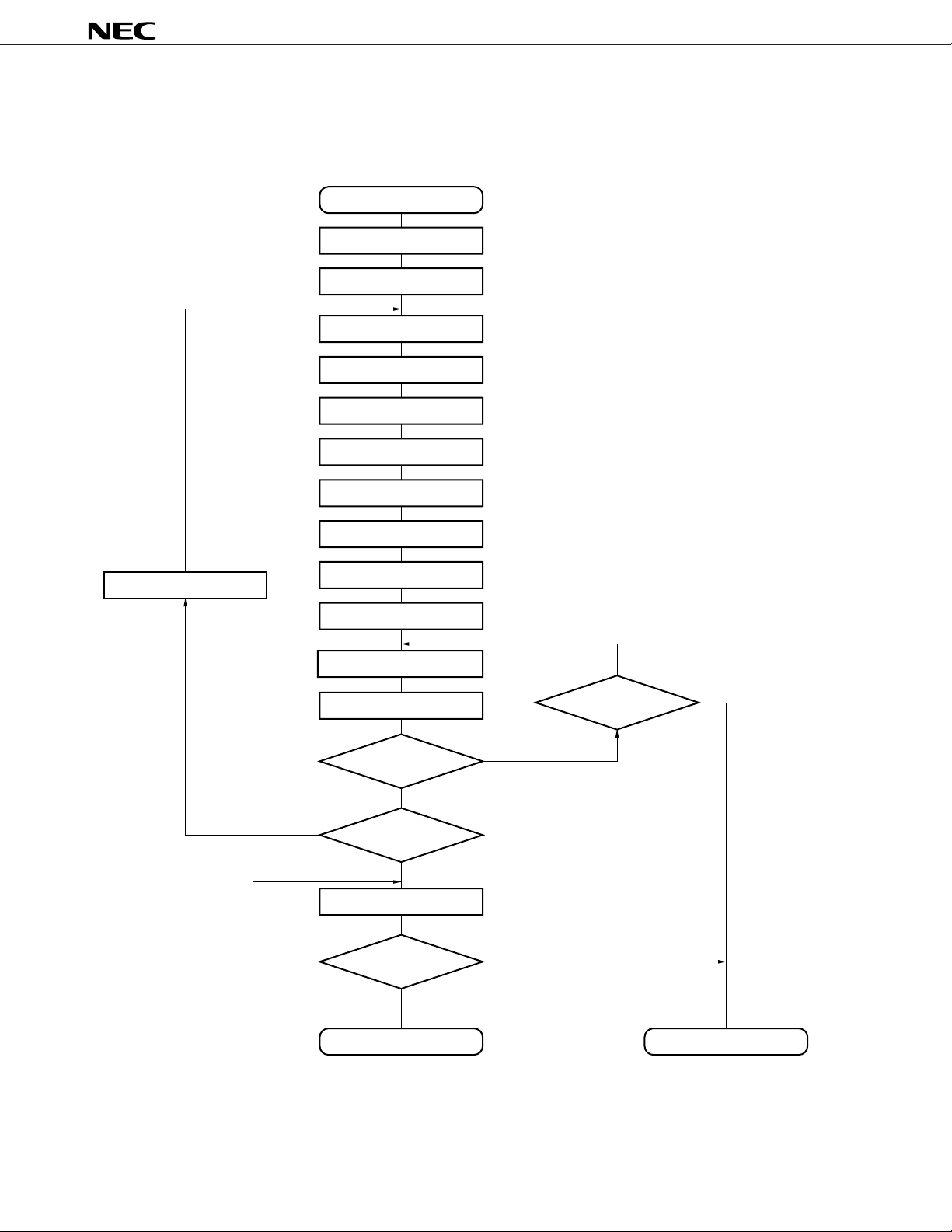
2.2 PROM Write Procedure
Figure 2-1. Page Program Mode Flow Chart
Start
Address = G
DD
= 6.5 V, V
V
Address = Address + 1
X = 0
Latch
Latch
PP
= 12.5 V
µ
PD178P018
Address = Address + 1
Address = Address + 1
Address = Address + 1
0.1-ms program pulse
No
Address = N?
V
DD
= 4.5 to 5.5 V, V
Latch
Latch
X = X + 1
Verify
4 bytes
Pass
Yes
PP
= V
No
X = 10?
Fail
DD
Yes
Remark G = Start address
N = Program last address
18
Pass
Verify
all bytes
All Pass
Write end Defective product
Fail
 Loading...