
DATA SHEET
MOS INTEGRATED CIRCUIT
µ
PD178F098
8-BIT SINGLE-CHIP MICROCONTROLLER
DESCRIPTION
The µPD178F098 is a flash memory model of the µPD178076, 178078, 178096, and 178098, and is provided with
a flash memory to/from which data can be written/erased with the microcontroller mounted on a printed circuit board.
For the detailed functional description, refer to the following User’s Manuals:
µ
PD178078, 178098 Subseries User’s Manual: U12790E
78K/0 Series User’s Manual - Instruction : U12326E
FEATURES
• Serial interface (UART mode)
• IEBusTM controller
• Pin-compatible with mask ROM models (except VPP pin)
• Flash memory: 60K bytes
• Internal high-speed RAM: 1024 bytes
• Internal extension RAM: 2048 bytes
• Buffer RAM: 32 bytes
• Operable at same supply voltage as mask ROM models (VDD = 4.5 to 5.5 V during PLL operation)
Note The capacities of the flash memory and internal extension RAM can be changed using the memory size
select register (IMS) and internal extension RAM size select register (IXS).
Remark For the differences between the flash memory model and mask ROM models, refer to 1. DIFFERENCES
BETWEEN
The electrical specifications (such as supply current) in the
mask ROM models. Confirm these differences before mass-producing any application set.
APPLICATION FIELD
Car stereos
Note
Note
µ
PD178F098 AND MASK ROM MODELS.
µ
PD178F098 differ from those of the
ORDERING INFORMATION
Part Number Package
µ
PD178F098GF-3BA 100-pin plastic QFP (14 × 20)
The information in this document is subject to change without notice. Before using this document, please
confirm that this is the latest version.
Not all devices/types available in every country. Please check with local NEC representative for availability
and additional information.
Document No. U12920EJ1V0DS00
Date Published June 2000 N CP(K)
Printed in Japan
The mark shows major revised points.
©
1997, 2000
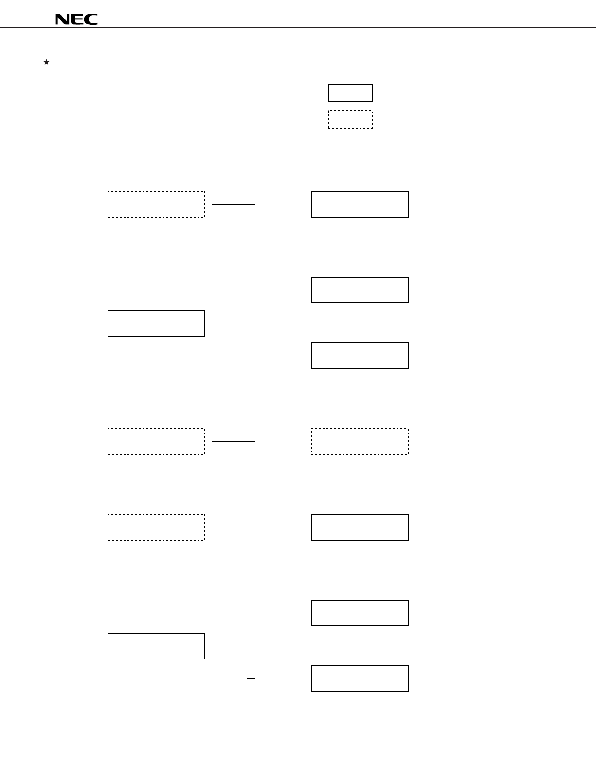
DEVELOPMENT OF 8-BIT DTS SERIES
µ
PD178F098
Models under mass production
Models under development
Flash memory model or
PROM model
80 pins 80 pins
100 pins
µ
PD178F048
Internal OSD controller
8-bit PWM × 4 channels
14-bit PWM × 1 channel
PD178F098
µ
Internal IEBus controller and UART
100 pins
100 pins
Mask ROM model
PD178048 subseries
µ
Internal OSD controller
8-bit PWM × 4 channels
14-bit PWM × 1 channel
PD178098 subseries
µ
Internal IEBus controller
PD178078 subseries
µ
Internal UART
80 pins
80 pins
80 pins
PD178F134
µ
Internal LCD and UART
PD178F124
µ
Internal UART Internal UART
PD178P018A
µ
80 pins
80 pins
80 pins
80 pins
µ
PD178034 subseries
Internal LCD and UART
µ
PD178024 subseries
µ
PD178018A subseries
PD178003 subseries
µ
Limits functions of
PD178018A subseries
µ
2
Data Sheet U12920EJ1V0DS00

µ
PD178F098
FUNCTIONAL OUTLINE
Item Functions
Internal Flash memory 60K bytes
memory High-speed RAM 1024 bytes
Buffer RAM 32 bytes
Extension RAM 2048 bytes
General-purpose register 8 bits × 32 registers (8 bits × 8 registers × 4 banks)
Minimum instruction execution • 0.32 µs/0.64 µs/1.27 µs/2.54 µs/5.08 µs (with crystal resonator of fX = 6.3 MHz)
time • 0.44 µs/0.89 µs/1.78 µs/3.56 µs/7.11 µs (with crystal resonator of fX = 4.5 MHz)
Instruction set • 16-bit operation
• Multiplication/division (8 bits × 8 bits, 16 bits ÷ 8 bits)
• Bit manipulation (set, reset, test Boolean operation)
• BCD adjustment, etc.
I/O port Total : 80 pins
• CMOS input : 8 pins
• CMOS I/O : 64 pins
• N-ch open-drain output : 8 pins
A/D converter 8-bit resolution × 8 channels
Serial interface • 3-wire/SBI/2-wire/I2C bus
• 3-wire mode : 1 channel
• 3-wire mode (with automatic transmit/receive function of up to 32 bytes): 1 channel
• UART mode : 1 channel
IEBus controller Provided
Timer • Basic timer (timer carry FF (10 Hz)) : 1 channel
• 16-bit timer/event counter : 1 channel
• 8-bit timer/event counter : 2 channels
• Watchdog timer : 1 channel
Buzzer output BEEP0 pin: 1 kHz, 1.5 kHz, 3 kHz, 4 kHz
BUZ pin: 0.77 kHz, 1.54 kHz, 3.08 kHz, 6.15 kHz (with crystal resonator of fX = 6.3 MHz)
Vectored Maskable Internal : 15, External: 8
interrupt Non-maskable Internal: 1
source Software 1
PLL Division mode 2 types
frequency • Direct division mode (VCOL pin)
synthesizer • Pulse swallow mode (VCOL and VCOH pins)
Reference Seven types selectable in software (1, 3, 9, 10, 12.5, 25, 50 kHz)
frequency
Charge pump Error out output: 2 pins
Phase Unlock detectable in software
comparator
Note 2
mode selectable : 1 channel
(1/2)
Note 1
Notes 1. When using the IEBus controller, the 4.5-MHz crystal resonator cannot be used. Use the 6.3-MHz
crystal resonator.
2. When the I2C bus mode is used (including when the mode is implemented in software without using
the peripheral hardware), consult NEC when ordering a mask.
Data Sheet U12920EJ1V0DS00
3

µ
PD178F098
(2/2)
Item Functions
Frequency counter Frequency measurement
• AMIFC pin: For 450-kHz counting
• FMIFC pin: For 450-kHz/10.7-MHz counting
Standby function • HALT mode
• STOP mode
Reset • Reset by RESET pin
• Internal reset by watchdog timer
• Reset by power-ON clear circuit
• Detection of less than 4.5 V
• Detection of less than 3.5 V
• Detection of less than 2.3 V
Supply voltage • VDD = 4.5 to 5.5 V (during CPU, PLL operation)
•VDD = 3.5 to 5.5 V (during CPU operation)
Package 100-pin plastic QFP (14 × 20)
Note
(Reset does not occur, however.)
Note
(during CPU operation)
Note
(in STOP mode)
Note These voltages are the maximum values. In practice, the chip may be reset at voltages lower than these.
4
Data Sheet U12920EJ1V0DS00
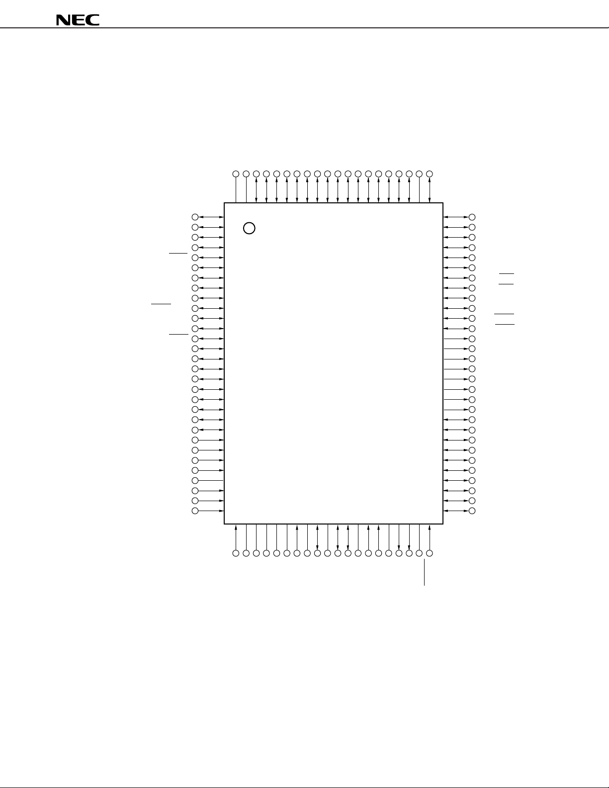
PIN CONFIGURATION (Top View)
• 100-pin plastic QFP (14 × 20)
µ
PD178F098GF-3BA
GNDPORT
PORT
DD
P47
V
P46
P45
P44
P43
P42
P41
P40
P67
P66
P65
P64
P63
P62
P61
P60
GND1
P07/INTP7
µ
PD178F098
P00/INTP0
P01/INTP1
P20/SI1
P21/SO1
P22/SCK1
P23/STB
P24/BUSY
P25/SI0/SB0/SDA0
P26/SO0/SB1/SDA1
P27/SCK0/SCL
P70/SI3
P71/SO3
P72/SCK3
P73
P50
P51
P52
P53
P54
P55
P56
P57
P10/ANI0
P11/ANI1
P12/ANI2
P13/ANI3
AV
P14/ANI4
P15/ANI5
P16/ANI6
100 99 98 97 96 95 94 93 92 91 90 89 88 87 86 85 84 83 82 81
1
2
3
4
5
6
7
8
9
10
11
12
13
14
15
16
17
18
19
20
21
22
23
24
25
26
DD
27
28
29
30
31 32 33 34 35 36 37 38 39 40 41 42 43 44 45 46 47 48 49 50
80
79
78
77
76
75
74
73
72
71
70
69
68
67
66
65
64
63
62
61
60
59
58
57
56
55
54
53
52
51
P06/INTP6
P05/INTP5
P04/INTP4
P124
P123
P122
P121/RX0
P120/TX0
P77
P76
P75/TXD0
P74/RXD0
P137
P136
P135
P134
P133
P132
P131/TO51
P130/TO50
P37/BUZ
P36/BEEP0
P35/TI51
P34/TI50
P33/TI01
P32/TI00
P31/TO0
P30/VM45
P03/INTP3
P02/INTP2
SS
AV
REGCPU
P17/ANI7
DD
V
REGOSC
X2
X1
P100
GND0
GND2
P102/FMIFC
P101/AMIFC
PLL
DD
V
VCOL
VCOH
GNDPLL
EO0
EO1
PP
V
RESET
Cautions 1. Directly connect the VPP pin to GND0, GND1, or GND2 in normal operating mode.
2. Keep the voltage at AV
DD, VDDPORT, and VDDPLL same as that at the VDD pin.
3. Keep the voltage at AVSS, GNDPORT, and GNDPLL same as that at GND0, GND1, or GND2.
4. Connect each of the REGOSC and REGCPU pins to GND via a 0.1-µF capacitor.
Data Sheet U12920EJ1V0DS00
5

Pin Name
AMIFC : AM intermediate frequency counter
input
ANI0-ANI7 : A/D converter input
DD : A/D converter power supply
AV
SS : A/D converter ground
AV
BUSY : Busy output
BEEP0, BUZ : Buzzer output
EO0, EO1 : Error out output
FMIFC : FM intermediate frequency counter
input
GNDPLL : PLL ground
GND0-GND2 : Ground
INTP0-INTP7 : Interrupt input
P00-P07 : Port 0
P10-P17 : Port 1
P20-P27 : Port 2
P30-P37 : Port 3
P40-P47 : Port 4
P50-P57 : Port 5
P60-P67 : Port 6
P70-P77 : Port 7
P100-P102 : Port 10
P120-P124 : Port 12
P130-P137 : Port 13
REGCPU : Regulator for CPU power supply
µ
PD178F098
REGOSC : Regulator for oscillation circuit
RESET : Reset input
RXD0 : UART0 serial data input
RX0 : IEBus serial data input
SB0, SB1 : Serial data bus input/output
SCK0, SCK1, SCK3
: Serial clock input/output
SCL : Serial clock input/output
SDA0, SDA1 : Serial data input/output
SI0, SI1, SI3 : Serial data input
SO0, SO1, SO3 : Serial data output
STB : Strobe output
TI00, TI01 : 16-bit timer capture trigger input
TI50, TI51 : 8-bit timer clock input
TO0 : 16-bit timer output
TO50, TO51 : 8-bit timer output
TXD0 : UART0 serial data output
TX0 : IEBus serial data output
VCOL, VCOH : Local oscillation input
DDPORT : Port power supply
V
VDDPLL : PLL power supply
DD : Power supply
V
VM45 : VDD = 4.5 V monitor output
VPP : Programming power supply
X1, X2 : Crystal resonator
6
Data Sheet U12920EJ1V0DS00
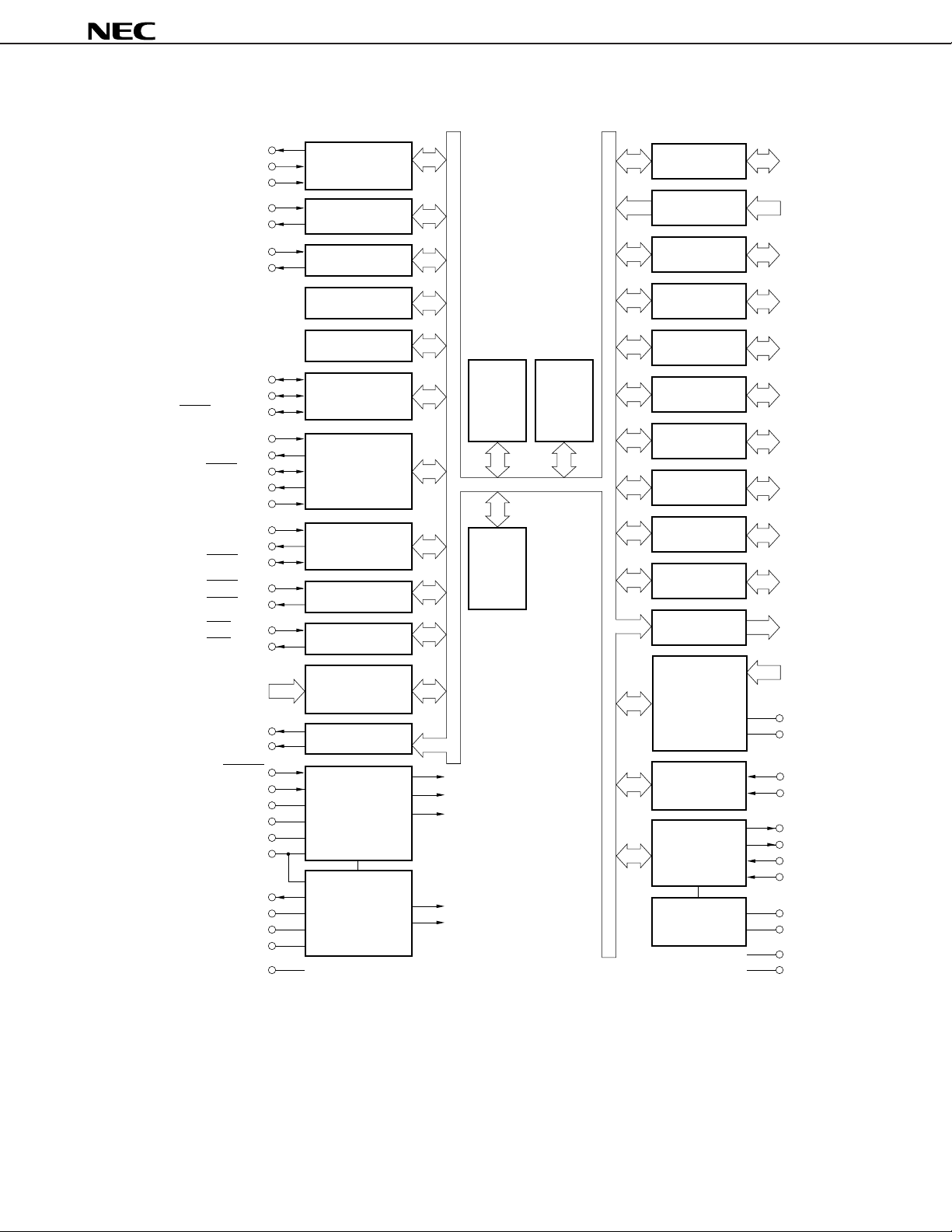
BLOCK DIAGRAM
µ
PD178F098
TO0/P31
TI00/P32
TI01/P33
TI50/P34
TO50/P130
TI51/P35
TO51/P131
SI0/SB0/SDA0/P25
SO0/SB1/SDA1/P26
SCK0/SCL/P27
SI1/P20
SO1/P21
SCK1/P22
STB/P23
BUSY/P24
SI3/P70
SO3/P71
SCK3/P72
RXD0/P74
TXD0/P75
RX0/P121
TX0/P120
INTP0/P00-
INTP7/P07
BEEP0/P36
BUZ/P37
16-bit TIMER/
EVENT COUNTER
8-bit TIMER/
EVENT COUNTER 50
8-bit TIMER/
EVENT COUNTER 51
WATCHDOG TIMER
BASIC TIMER
SERIAL
INTERFACE 0
SERIAL
INTERFACE 1
SERIAL
INTERFACE 3
UART0
IEBus0
INTERRUPT
8
CONTROL
BUZZER OUTPUT
78K/0
CPU
CORE
RAM
(3K bytes)
FLASH
MEMORY
(60K bytes)
PORT 0
PORT 1
PORT 2
PORT 3
PORT 4
PORT 5
PORT 6
PORT 7
PORT10
PORT 12
PORT 13
A/D
CONVERTER
8
8
8
8
8
8
8
8
3
5
8
8
P00-P07
P10-P17
P20-P27
P30-P37
P40-P47
P50-P57
P60-P67
P70-P77
P100-P102
P120-P124
P130-P137
ANI0/P10ANI7/P17
AV
DD
AV
SS
RESET
X1
X2
DD
PORT
V
GNDPORT
V
VM45/P30
REGOSC
REGCPU
GND0
GND1
RESET
SYSTEM
CONTROL
DD
CPU
PERIPHERAL
FREQUENCY
COUNTER
PLL
AMIFC/P101
FMIFC/P102
EO0
EO1
VCOL
VCOH
V
VOLTAGE
REGULATOR
OSC
V
CPU
PLL
VOLTAGE
REGULATOR
DD
PLL
V
GNDPLL
IC
GND2
Data Sheet U12920EJ1V0DS00
7

µ
PD178F098
CONTENTS
1. DIFFERENCES BETWEEN µPD178F098 AND MASK ROM MODELS ..................................... 9
2. PIN FUNCTION LIST...................................................................................................................... 10
2.1 Port Pins .................................................................................................................................. 10
2.2 Pins Other Than Port Pins ......................................................................................................11
2.3 I/O Circuits of Pins and Recommended Connections of Unused Pins ............................. 13
3. MEMORY SIZE SELECT REGISTER (IMS)................................................................................. 17
4. INTERNAL EXTENSION RAM SIZE SELECT REGISTER (IXS) .............................................. 18
5. INTERRUPT FUNCTION ................................................................................................................. 19
6. FLASH MEMORY PROGRAMMING .............................................................................................. 23
6.1 Selecting Communication Mode ........................................................................................... 23
6.2 Flash Memory Programming Function ................................................................................. 24
6.3 Connecting Flashpro III .......................................................................................................... 25
7. ELECTRICAL SPECIFICATIONS ................................................................................................... 26
8. PACKAGE DRAWING ..................................................................................................................... 44
9. RECOMMENDED SOLDERING CONDITIONS ............................................................................. 45
APPENDIX A. DEVELOPMENT TOOLS ............................................................................................... 46
APPENDIX B. RELATED DOCUMENTS .............................................................................................. 48
8
Data Sheet U12920EJ1V0DS00

µ
PD178F098
1. DIFFERENCES BETWEEN µPD178F098 AND MASK ROM MODELS
The µPD178F098 is provided with a flash memory to/from which data can be written/erased with the device
mounted on a printed circuit board. The differences between the flash memory model (µPD178F098) and mask ROM
µ
models (
PD178076, 178078, 178096, and 178098) are shown in Table 1-1.
µ
Table 1-1. Differences between
PD178F098 and Mask ROM Models
Item
Internal memory ROM structure Flash memory Mask ROM
ROM capacity 60K bytes
External 2048 bytes
extension RAM
Internal ROM capacity selected by Equivalent to mask ROMµPD178076: CCH
memory size select register (IMS) model
Internal extension RAM capacity Equivalent to mask ROMµPD178076: 0AH
selected by internal extension RAM model
size select register (IXS)
Serial interface 4 channels 3 channels
IEBus controller Provided Not provided Provided
Interrupt source 24 22 21
IC pin Not provided Provided
VPP pin Provided Not provided
Electrical specifications and See the relevant data sheet
recommended soldering conditions
µ
PD178F098
• 3-wire/SBI/2-wire/I2C bus mode selectable • 3-wire/SBI/2-wire/I2C bus
• 3-wire (with automatic transmit/receive function) mode selectable
• 3-wire • 3-wire (with automatic
• UART transmit/receive function)
µ
PD178076, 178078
µ
PD178076: 48K bytes
µ
PD178078: 60K bytes
µ
PD178076: 1024 bytes
µ
PD178078: 2048 bytes
µ
PD178078: CFH
µ
PD178078: 08H
µ
PD178096, 178098
µ
PD178096: 48K bytes
µ
PD178098: 60K bytes
µ
PD178096: 1024 bytes
µ
PD178098: 2048 bytes
µ
PD178096: CCH
µ
PD178098: CFH
µ
PD178096: 0AH
µ
PD178098: 08H
• 3-wire
Caution The noise resistance and noise radiation differ between flash memory versions and mask ROM
versions. When considering the replacement of flash memory versions with mask ROM versions
in the process from trial manufacturing to mass production, adequate evaluation should be carried
out using CS products (not ES products) of mask ROM versions.
Data Sheet U12920EJ1V0DS00
9

µ
PD178F098
2. PIN FUNCTION LIST
2.1 Port Pins (1/2)
Pin Name I/O Function At Reset Shared by:
P00-P07 I/O Port 0. Input INTP0-INTP7
8-bit I/O port.
Can be set in input or output mode in 1-bit units.
P10-P17 Input Port 1. Input ANI0-ANI7
8-bit input port.
P20 I/O Port 2. Input SI1
P21 8-bit I/O port. SO1
P22 Can be set in input or output mode in 1-bit units. SCK1
P23 STB
P24 BUSY
P25 SI0/SB0/SDA0
P26 SO0/SB1/SDA1
P27 SCK0/SCL
P30 I/O Port 3. Input VM45
P31 8-bit I/O port. TO0
P32 Can be set in input or output mode in 1-bit units. TI00
P33 TI01
P34 TI50
P35 TI51
P36 BEEP0
P37 BUZ
P40-47 I/O Port 4. Input –
8-bit I/O port.
Can be set in input or output mode in 1-bit units.
P50-P57 I/O Port 5. Input –
8-bit I/O port.
Can be set in input or output mode in 1-bit units.
P60-P67 I/O Port 6. Input –
8-bit I/O port.
Can be set in input or output mode in 1-bit units.
P70 I/O Port 7. Input SI3
P71 8-bit I/O port. SO3
P72 Can be set in input or output mode in 1-bit units. SCK3
P73 –
P74 RXD0
P75 TXD0
P76, P77 –
10
Data Sheet U12920EJ1V0DS00
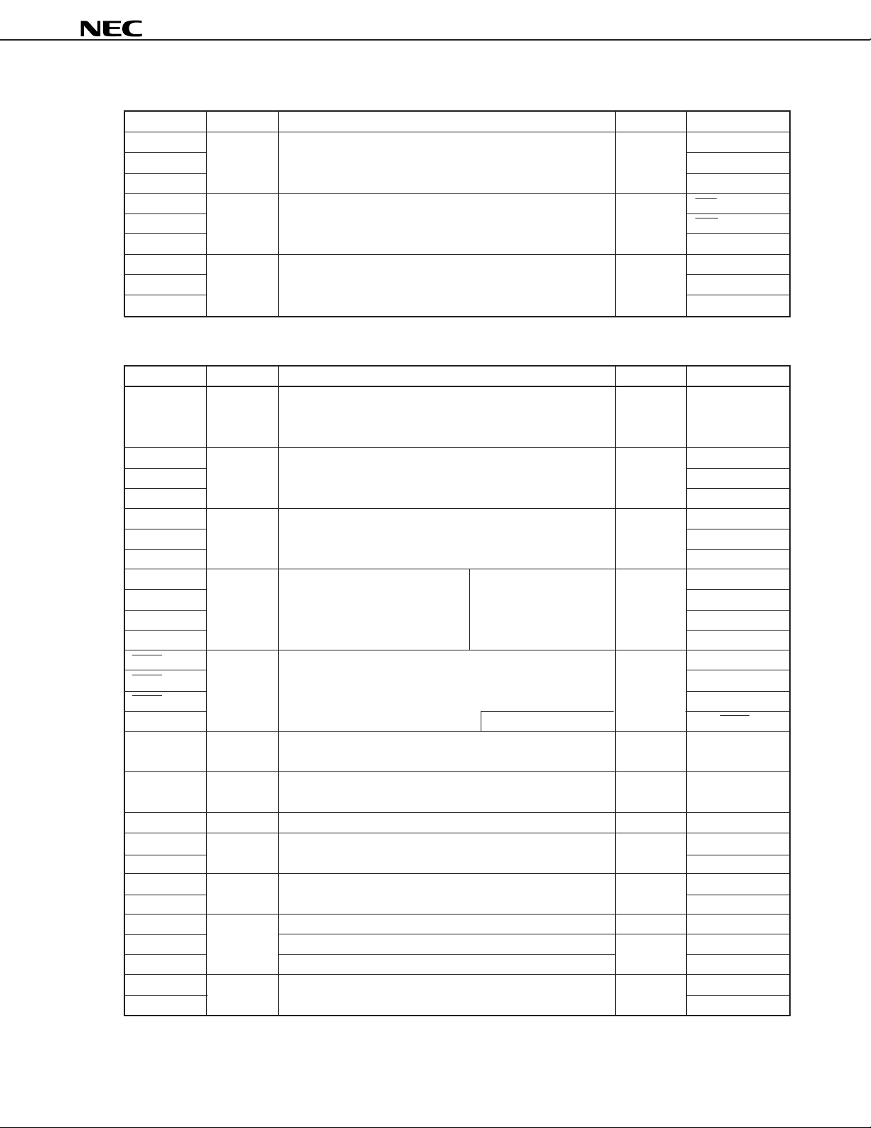
µ
PD178F098
2.1 Port Pins (2/2)
Pin Name I/O Function At Reset Shared by:
P100 I/O Port 10. Input –
P101 3-bit I/O port. AMIFC
P102 Can be set in input or output mode in 1-bit units. FMIFC
P120 I/O Port 12. Input TX0
P121 5-bit I/O port. RX0
P122-P124 Can be set in input or output mode in 1-bit units. –
P130 Output Port 13. Low-level TO50
P131 8-bit output port. output TO51
P132-P137 N-ch open-drain output port (15 V withstand) –
2.2 Pins Other Than Port Pins (1/2)
Pin Name I/O Function At Reset Shared by:
INTP0-INTP7 Input External maskable interrupt input whose valid edge Input P00-P07
(rising edge, falling edge, or both rising and falling edges)
can be specified.
SI0 Input Serial data input to serial interface. Input P25/SB0/SDA0
SI1 P20
SI3 P70
SO0 Output Serial data output from serial interface. Input P26/SB1/SDA1
SO1 P21
SO3 P71
SB0 I/O Serial data input/output to/from N-ch open drain I/O Input P25/SI0/SDA0
SB1 serial interface. P26/SO0/SDA1
SDA0 P25/SI0/SB0
SDA1 P26/SO0/SB1
SCK0 I/O Serial clock input/output to/from serial interface. Input P27/SCL
SCK1 P22
SCK3 P72
SCL N-ch open drain I/O P27/SCK0
STB Output Strobe output for serial interface automatic transmission/ Input P23
reception.
BUSY Input Busy input for serial interface automatic transmission/ Input P24
reception.
VW45 Output VDD = 4.5 V monitor output Input P30
TI00 Input External count clock input to 16-bit timer (TM0). Input P32
TI01 P33
TI50 Input External count clock input to 8-bit timer (TM50). Input P34
TI51 External count clock input to 8-bit timer (TM51). P35
TO0 Output 16-bit timer (TM0) output. Input P31
TO50 8-bit timer (TM50) output. Low-level P130
TO51 8-bit timer (TM51) output. output P131
BEEP0 Output Buzzer output. Input P36
BUZ P37
Data Sheet U12920EJ1V0DS00
11

µ
PD178F098
2.2 Pins Other Than Port Pins (2/2)
Pin Name I/O Function At Reset Shared by:
ANI0-ANI7 Input Analog input to A/D converter. Input P10-P17
EO0, EO1 Output Error out output from charge pump of PLL frequency – –
synthesizer.
VCOL Input Inputs local oscillation frequency of PLL (in HF and MF – –
modes).
VCOH Input Inputs local oscillation frequency of PLL (in VHF mode). – –
AMIFC Input Input to AM intermediate frequency counter. Input P101
FMIFC Input Input to FM intermediate frequency or AM intermediate Input P102
frequency counter.
RXD0 Input Serial data input to asynchronous serial interface (UART0). Input P74
TXD0 Output Serial data output from asynchronous serial interface Input P75
(UART0).
TX0 Output IEBus controller data output. Input P120
RX0 Input IEBus controller data input. Input P121
RESET Input System reset input. – –
X1 Input Connection of crystal resonator for system clock oscillation. – –
X2 – ––
REGOSC – Regulator for oscillation circuit. Connect this pin to GND via – –
0.1-µF capacitor.
REGCPU – Regulator for CPU power supply. Connect this pin to GND – –
via 0.1-µF capacitor.
VDD – Positive power supply. – –
GND0-GND2 – Ground. – –
VDDPORT – Port power supply. – –
GNDPORT – Port ground. – –
AVDD – A/D converter positive power supply. Keep voltage at this – –
pin same as that at VDD0.
AVSS – A/D converter ground. Keep voltage at this pin same as – –
that at GND0 through GND2.
Note
VDDPLL
GNDPLL
VPP – Pin to apply high voltage at program writing/verifying. – –
Note
– PLL positive power supply. – –
– PLL ground. – –
Directly connect this pin to GND0, GND1, or GND2 in
normal operating mode.
Note Connect a capacitor of about 1000 pF between the VDDPLL and GNDPLL pins.
12
Data Sheet U12920EJ1V0DS00

µ
PD178F098
2.3 I/O Circuits of Pins and Recommended Connections of Unused Pins
Table 2-1 shows the types of the I/O circuits of the respective pins and the recommended connections of the pins
when they are not used.
For the configuration of the I/O circuit of each pin, refer to Figure 2-1.
Table 2-1. I/O Circuit Type of Each Pin (1/2)
Pin Name I/O Circuit Type I/O Recommended Connection of Unused Pin
P00/INTP0-P07/INTP7 8 I/O Input: Connect each of them to VDD, VDDPORT, GND0 to
GND2, or GNDPORT via resistor.
Output: Leave open.
P10/ANI0-P17/ANI7 25 Input Connect these pins to VDD, VDDPORT, GND0 to GND2 or
GNDPORT.
P20/SI1 5-K I/O Input: Connect each of them to VDD, VDDPORT, GND0 to
P21/SO1 5
P22/SCK1 5-K
P23/STB 5
P24/BUSY 5-K
P25/SI0/SB0/SDA0 10-D
P26/SO0/SB1/SDA1
P27/SCK0/SCL
P30/VM45 5
P31/TO0
P32/TI00 5-K
P33/TI01
P34/TI50
P35/TI51
P36/BEEP0 5
P37/BUZ
P40-P47
P50-P57
P60-P67
P70/SI3 5-K
P71/SO3 5
P72/SCK3 5-K
P73 5
P74/RXD0 5-K
P75/TXD0 5
P76, P77
P100
P101/AMIFC
P102/FMIFC
P120/TX0
P121/RX0 5-K
P122-P124 5
GND2, or GNDPORT via resistor.
Output: Leave open.
Data Sheet U12920EJ1V0DS00
13

µ
PD178F098
Table 2-1. I/O Circuit Type of Each Pin (2/2)
Pin Name I/O Circuit Type I/O Recommended Connection of Unused Pin
P130/TO50 19 Output Open these pins.
P131/TO51
P132-P137
EO0 DTS-EO1
EO1
VCOL, VCOH DTS-AMP2 Input Disable PLL in software and select pull-down.
REGOSC, REGCPU – – Connect these pins to GND0, GND1, or GND2 via 0.1-µF
capacitor.
RESET 2 Input –
AVDD – – Connect this pin to VDD or VDDPORT.
AVSS Directly connect these pins to GND0 to GND2, or GNDPORT.
VPP
14
Data Sheet U12920EJ1V0DS00
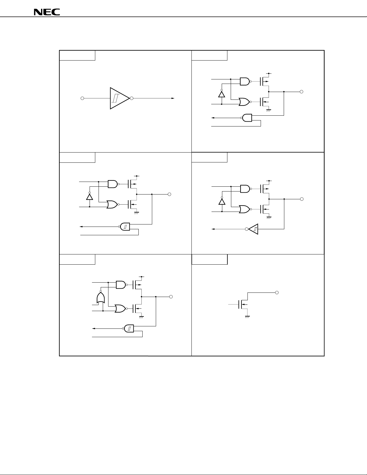
Figure 2-1. I/O Circuits of Respective Pins (1/2)
µ
PD178F098
Type 2
IN
Schmitt trigger input with hysteresis characteristics
Type 5-K
V
DD
data
output
disable
P-ch
N-ch
IN/OUT
Type 5
data
output
disable
input
enable
Type 8
data
output
disable
V
V
DD
P-ch
IN/OUT
N-ch
DD
P-ch
IN/OUT
N-ch
input
enable
Type 10-D
data
open drain
output disable
input
enable
Remark V
Type 19
V
DD
P-ch
IN/OUT
N-ch
DD and GND are the positive power supply and ground pins for all port pins. Take VDD and GND as
N-ch
OUT
VDDPORT and GNDPORT.
Data Sheet U12920EJ1V0DS00
15
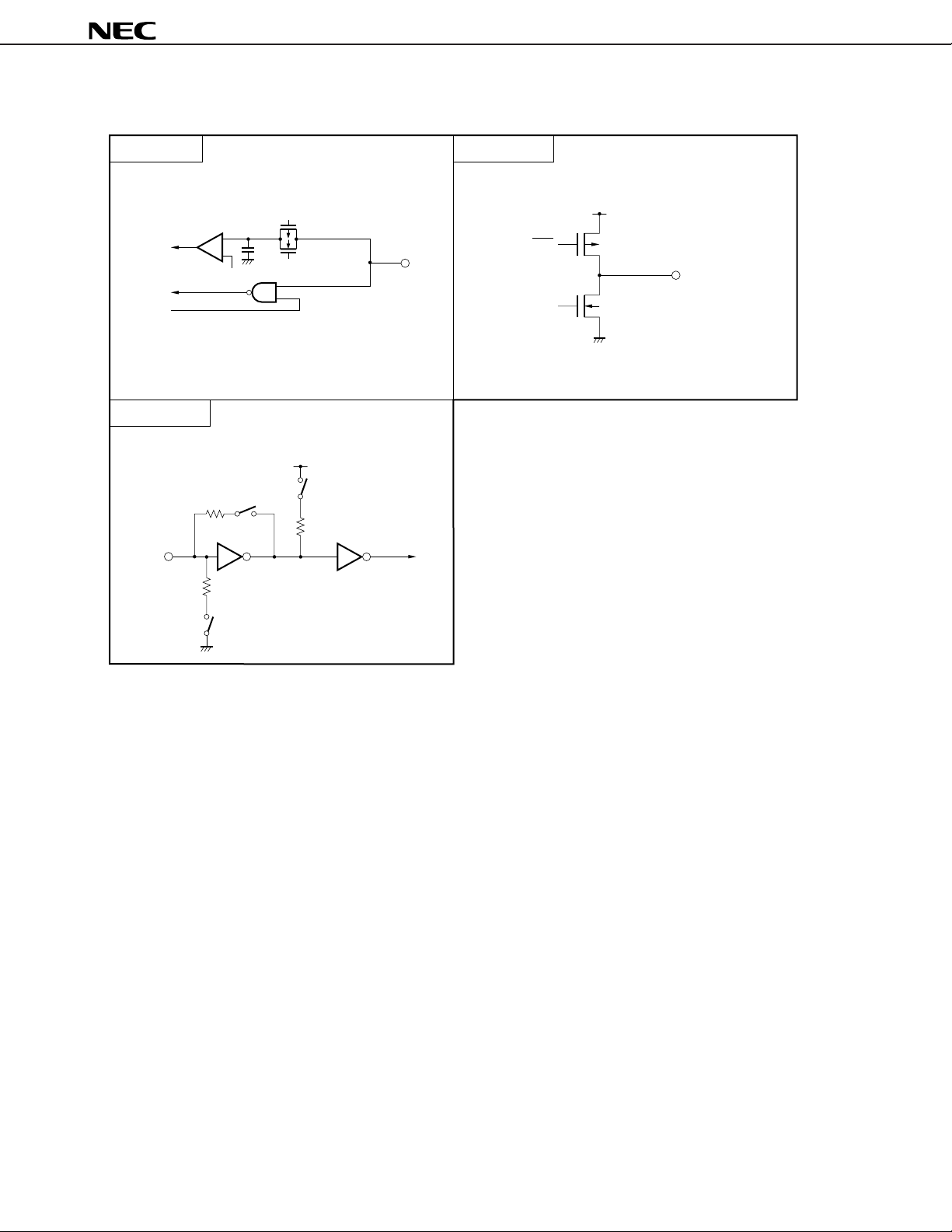
Figure 2-1. I/O Circuits of Respective Pins (2/2)
µ
PD178F098
Type 25
Comparator
input
enable
Type DTS-AMP
IN
P-ch
+
–
N-ch
V
REF (Threshold voltage)
VDDPLL
IN
Type DTS-EO1
DW
UP
DDPLL
V
P-ch
OUT
N-ch
GNDPLL
Note
GNDPLL
Note This switch is selectable in software only for the VCOL and VCOH pins.
Remark VDD and GND are the positive power supply and ground pins for all port pins. Take VDD and GND as
VDDPORT and GNDPORT.
16
Data Sheet U12920EJ1V0DS00
 Loading...