
DATA SHEET
BIPOLAR ANALOG INTEGRATED CIRCUIT
µ
PC1862
BURST LOCK CLOCK GENERATOR
The µPC1862 is an LSI incorporating a PLL circuit to generate nfSC clocks (fSC: color subcarrier frequency), ideal
for the processing of digital video signals as in extended definition television (EDTV) systems.
FEATURES
• VCO is incorporated.
• Horizontal and vertical sync separation circuits are incorporated (with output pins).
• Horizontal and vertical sync output pulses (TTL level)
• ACC amplifier and killer detector circuits are incorporated.
• 1/4 and 1/8 (1/2 × 1/4) frequency dividers are incorporated.
SC phase control circuits is incorporated.
•f
• Applicable to both NTSC and PAL systems.
• Possible to input burst gate pulse from external
ORDERING INFORMATION
Part number Package
µ
PC1862GS 36-pin plastic shrink SOP (300 mil)
Document No. S11431EJ3V0DS00 (3rd edition)
Date Published December 1997 N CP(K)
Printed in Japan
The information in this document is subject to change without notice.
The mark shows major revised points.
©
1991, 1996
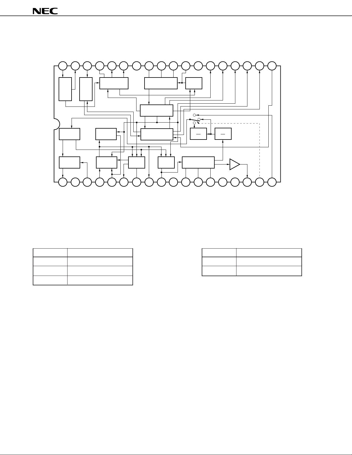
BLOCK DIAGRAM
µ
PC1862
SSI
CSO
VSSI
HDF
HDO
SGND
HKO
36 35 34 33 32 31 30 29 28 27 26 25 24 23 22 21 20 19
H
sync
SEP
Phase
shift
LPF
V
sync
SEP
ACC
DET
ACC
AMP
Color
Killer DET
1 2 3 4 5 6 7 8 9101112131415161718
SCO
CV
CC1
TINT
CIN
ACCF
CKF
CKO
Remark AFC : Automatic Frequency Control
ACC : Automatic Color saturation level Control
APC : Automatic Phase Control
HSOF2
HSOF1
H count down
V count down
APCF
COUT
HSOF3
APC
CGND
AFCF
SCOF1
SV
CC
AFC32fH VCOH DET
f
2
nfSC VCO
SCOF2
BGPE
SCOF3
NHSO
f
4
CV
CC2
CPO
CV
CC3
FIO
VCOO
VSO
N/P
DIVS
ESCI
Selecting divide ratio by DIVS pin Selecting TV transmission by N/P pin
DIVS Divide ratio N/P pin TV transmission
H 1/8 H PAL
Open EXT IN with pin 18 L NTSC
L 1/4
In PAL, only correspond 4fSC (DIVS = L).
2

System Block Diagram
Application to Process of Digital Video Signal
Analog
video input
A/D converter
PC659A
µ
Gate array, etc
Processing of
digital video
Clock
generator
PC1862
µ
D/A converter
µ
PC665 (1ch.)
µ
PC664 (2ch.)
µ
PC662 (3ch.)
µ
PC1862
Analog
video output
3
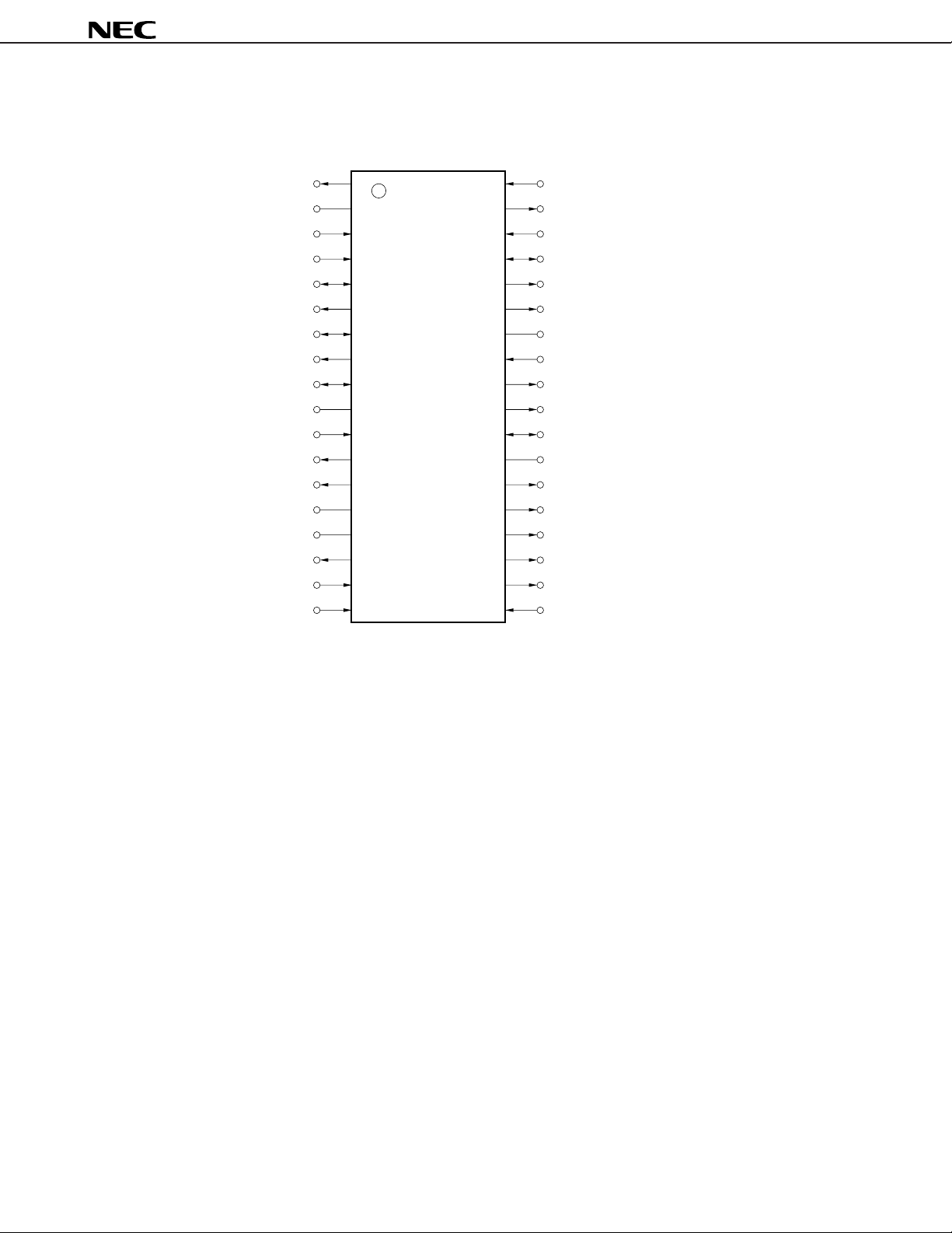
PIN CONFIGURATION (Top View)
36-pin plastic shrink SOP (300 mil)
µ
PC1862
SCO
CC1
TINT
CC2
CC3
1
2CV
3
4CIN
5ACCF
6CKO
7CKF
8COUT
9APCF
10CGND
11SCOF1
12SCOF2
13SCOF3
14CV
15CV
16VCOO
17DIVS
18ESCI
36
35 CSO
34
33 HDF
32 HDO
31 HKO
30 SGND
29 HSOF1
28 HSOF2
27 HSOF3
26 AFCF
25 SV
24 BGPE
23 NHSO
22 CPO
21 FIO
20 VSO
19 N/P
SSI
VSSI
CC
4

ACCF : Chroma ACC Filter
AFCF : Horizontal Sync AFC Filter
APCF : Chroma APC Filter
BGPE : Burst Gate Pulse from External
CGND : Chroma GND
CIN : Chroma Input
CKF : Color Killer Filter
CKO : Color Killer Output
COUT : Chroma Output
CPO : Clamp Pulse Output
CSO : Composite Sync Output
CC1-CVCC3 : Chroma VCC
CV
DIVS : Divider Setting Input
ESCI : External Subcarrier Input
FIO : Field ID Output
HDF : Horizontal Sync Detect Filter
HDO : Horizontal Sync Detect Output
HKO : Horizontal Sync Killer Output
HSOF1-HSOF3 : 32f
H VCO Filter
NHSO : Negative Horizontal Sync Output
N/P : NTSC/PAL Mode Select
SCO : Subcarrier Output
SCOF1-SCOF3 : f
SC VCO Filter
SGND : Sync GND
SSI : Horizontal Sync Separation Input
CC : Sync VCC
SV
TINT : Tint Control
VCOO : VCO Output
VSO : Vertical Sync Output
VSSI : Vertical Sync Separation Input
µ
PC1862
5
µ
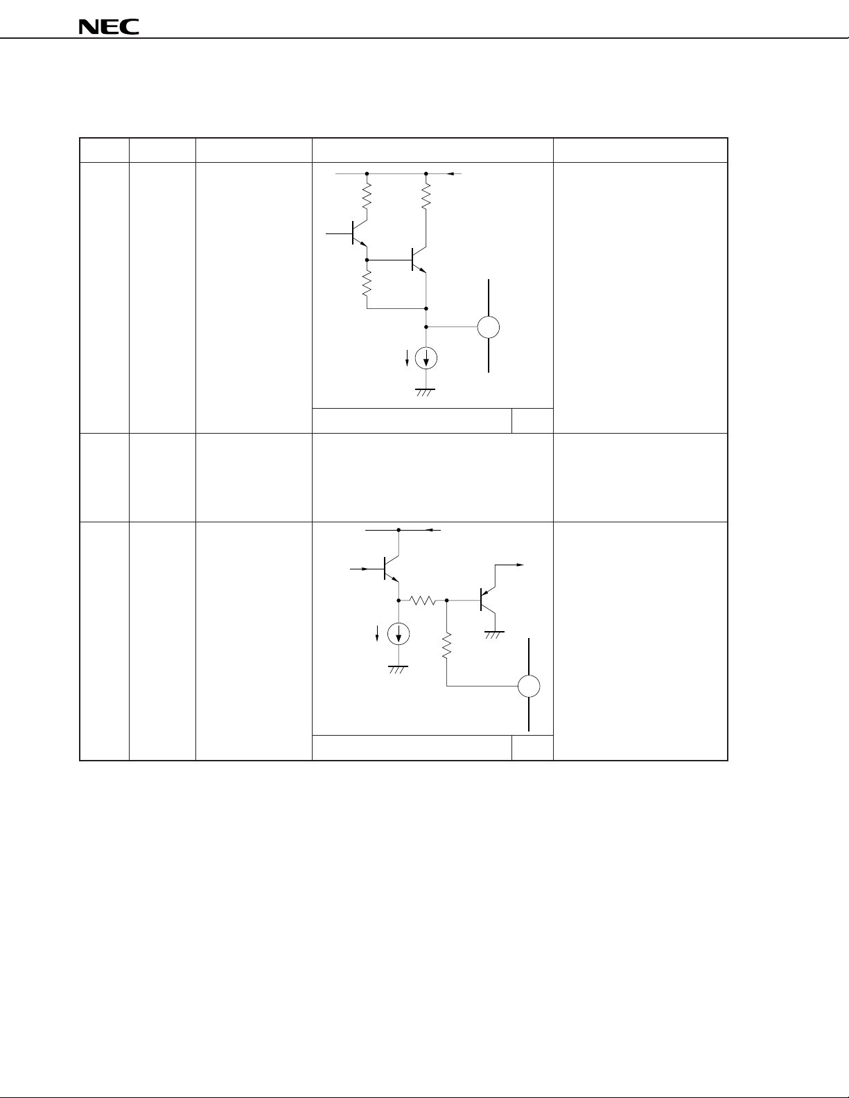
PIN FUNCTIONS
Pin No. Symbol Pin Name Equivalent Circuit Function
1 SCO Sub Carrier Output Burst locked sub carrier output
5 kΩ
µ
400 A
DC voltage of a standard 2.9 V
2CVCC1 Chroma VCC1 Power supply for chroma signal
3 TINT Tint Control Tint control input (DC voltage)
3.3 V
5 kΩ
CV
CC3 (pin 15)
CV
CC3
(pin 15)
1
processing circuit (pin 1 to pin 18)
This power supply must be
isolated from the power supply
for sync processing circuit use.
This pin adjusts the tint of sub
carrier output (SCO pin).
PC1862
(1/12)
100 A
µ
15 kΩ
3
Internal bias voltage of a standard 2.5 V
6
µ
PC1862
(2/12)
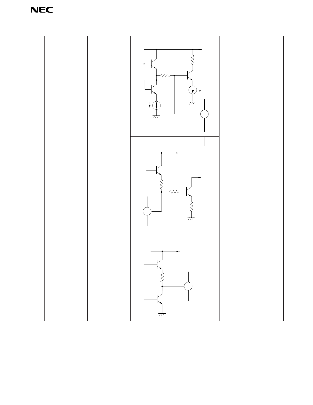
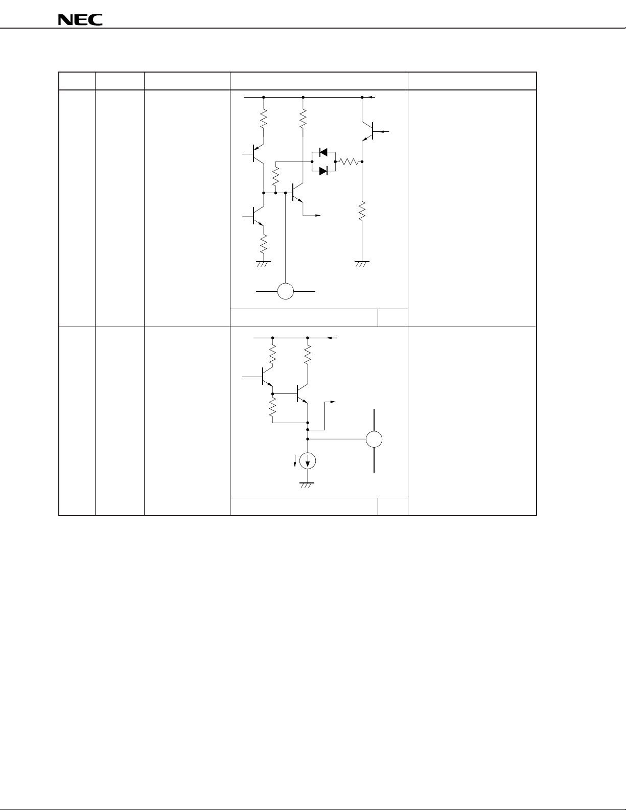
Pin No. Symbol Pin Name Equivalent Circuit Function
4 CIN Chroma Signal Input Chroma signal input
4.0 V
10 kΩ
200 A
µ
Internal bias voltage of a standard 3.2 V
5 ACCF Chroma ACC Filter Pin for connecting filter of ACC
5 kΩ
CV
CC3
100 A
4
(pin 15)
CV
CC1
(pin 2)
µ
(Automatic Color Control)
detector
2 kΩ
5
DC voltage of a standard
6 CKO Color Killer Output Color Killer Detection output
200 Ω
1 kΩ
2 kΩ
CV
CC3
(pin 15)
6
Note
1.0 V
When Killer (without burst) signal:
Low level output
When color signal: High level
output
Note Chroma burst amplitude from pin 4: 150 mVp-p
7
µ
PC1862
(3/12)
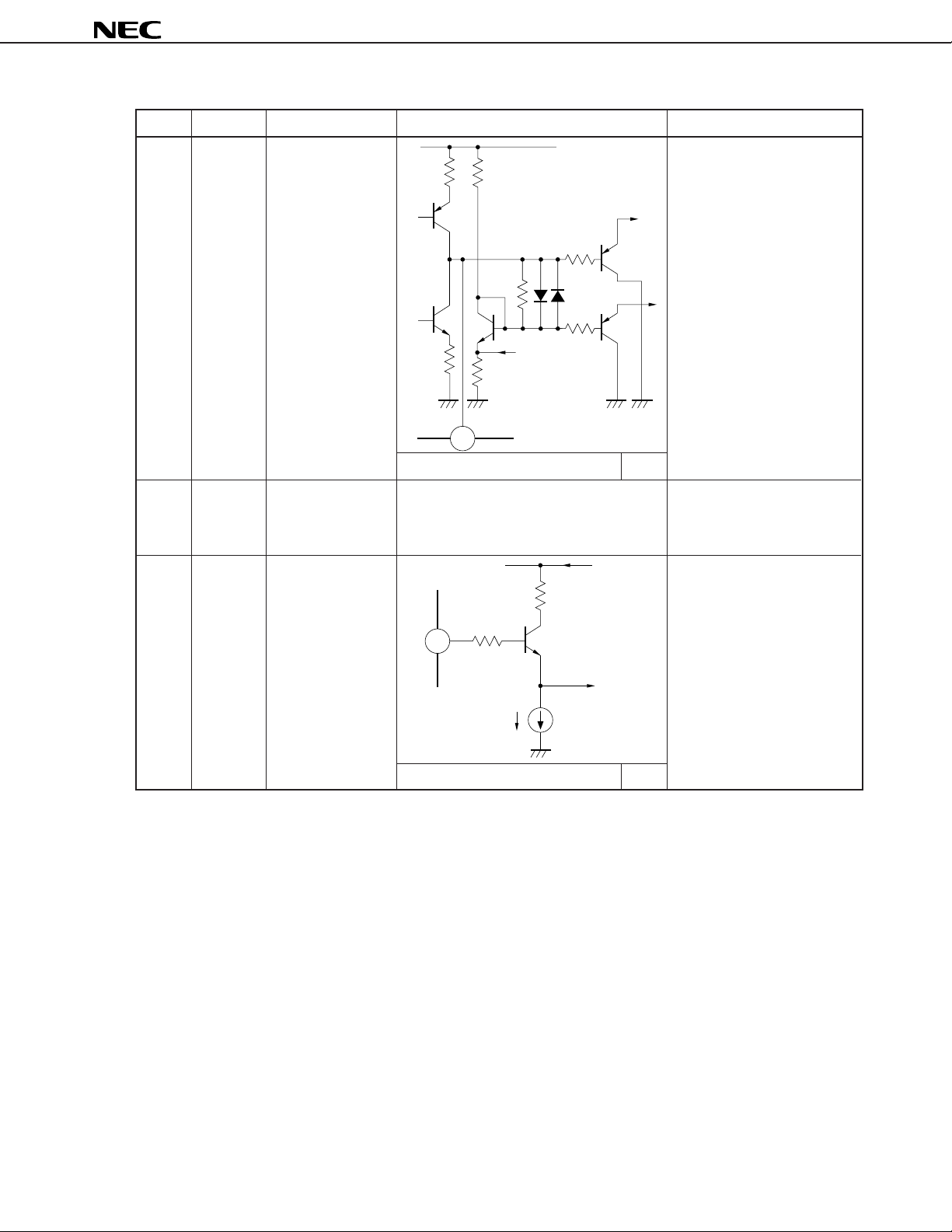
Pin No. Symbol Pin Name Equivalent Circuit Function
CC3
7 CKF Chroma Killer Filter Pin for connecting filter of Color
1 kΩ
2 kΩ
500 Ω
14 kΩ
1 kΩ
7
CV
(pin 15)
3.6 V
killter detector
DC voltage of a standard
8 COUT Chroma Signal Automatic color controlled chroma
Output output
5 kΩ
µ
400 A
DC voltage of a standard 2.4 V
Note
2.2 V
CV
CC3
(pin 15)
For APC circuit
8
Note Chroma burst amplitude from pin 4: 150 mVp-p
8
µ
PC1862
(4/12)
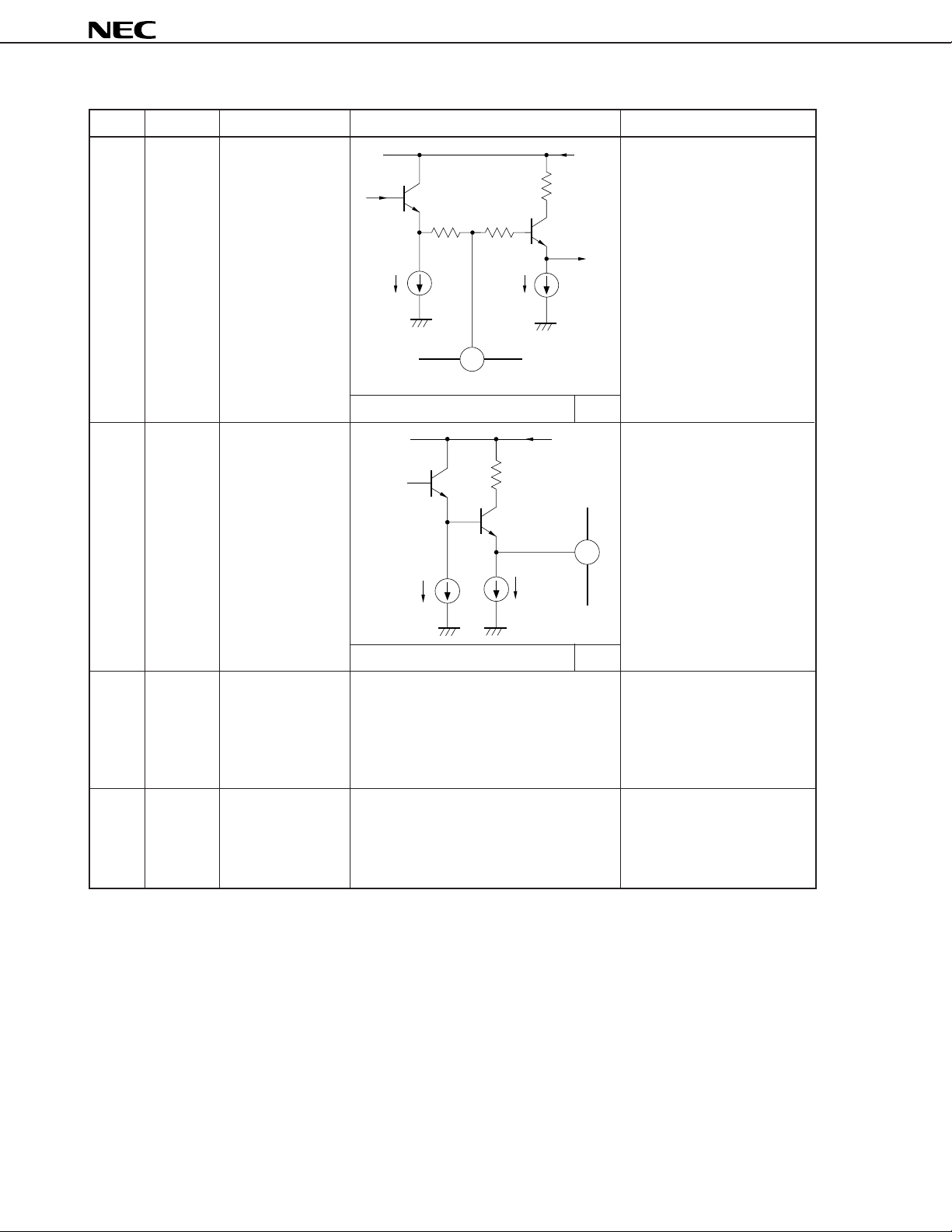
Pin No. Symbol Pin Name Equivalent Circuit Function
9 APCF APC Filter Pin for connecting filter of APC
1 kΩ 12 kΩ
60 k
Ω
5 kΩ
65 kΩ
(Automatic Phase Control)
detector
4.5 kΩ
µ
1.8 V
Note
CV
CC2
(pin 14)
2.7 V
processing circuit (pin 1 to pin 18)
VCO
1 kΩ
9
DC voltage of a standard
10 CGND Chroma GND Ground for chroma signal
11 SCOF1 nfSC VCO Filter (1) Pin for connecting filter of nfSC
500 Ω
11
200 A
Bias voltage of a standard 3.0 V
Note Chroma burst amplitude from pin 4: 150 mVp-p
9
µ
PC1862
(5/12)
Pin No. Symbol Pin Name Equivalent Circuit Function
12 SCOF2 nfSC VCO Filter (2) Pin for connecting filter of nfSC
3.8 V
20 kΩ 1 kΩ
1 kΩ
CV
CC2
(pin 14)
VCO
200 A 200 A
Internal bias voltage of a standard 3.0 V
13 SCOF3 nfSC VCO Filter (3) Pin for connecting filter of nfSC
200 A
µ
DC voltage of a standard 2.9 V
14 CVCC2 Chroma VCC 2 Power supply for chroma signal
12
µµ
1 mA
CV
CC2
(pin 14)
13
VCO
processing circuit (pin 1 to pin 18)
This power supply must be
isolated from the power supply
for sync processing circuit use.
15 CVCC3 Chroma VCC 3 Power supply for chroma signal
processing circuit (pin 1 to pin 18)
This power supply must be
isolated from the power supply
for sync processing circuit use.
10
 Loading...