NEC UPC1853CT-02, UPC1853CT-01 Datasheet

DATA SHEET
BIPOLAR ANALOG INTEGRATED CIRCUIT
µ
PC1853
MATRIX SURROUND IC WITH I2C BUS
The µPC1853 is a phase shift matrix surround IC. Only 2 speakers on the front side implement wide sound
expansion, and by adding rear speakers, rich three-dimensional sound can obtained.
The µPC1853 can perform all controls (mode switching, volume control and so on) through the I2C bus.
FEATURES
• Any control is possible through the I2C bus.
• Surround effect can be realized by only 2 speakers on the front side.
• On-chip tone (bass and treble) control circuit.
• Level-adjustable output pin for heavy bass sound.
• Level-adjustable output pin for AV amplifier.
µ
PC1853-01 : On-chip low boost circuit.
•
On-chip volume and balance control circuits.
µ
PC1853-02 : On-chip L-channel volume and R-channel volume control circuits.
•
APPLICATION
• TV, audio
ORDERING INFORMATION
Part Number Package
µ
PC1853CT-01 30-pin plastic shrink DIP (400 mil)
µ
PC1853CT-02
"
The information in this document is subject to change without notice.
Document No. S10552EJ2V0DS00 (2nd edition)
(Previous No. ID-3126)
Date Published October 1995 P
Printed in Japan
©
1995
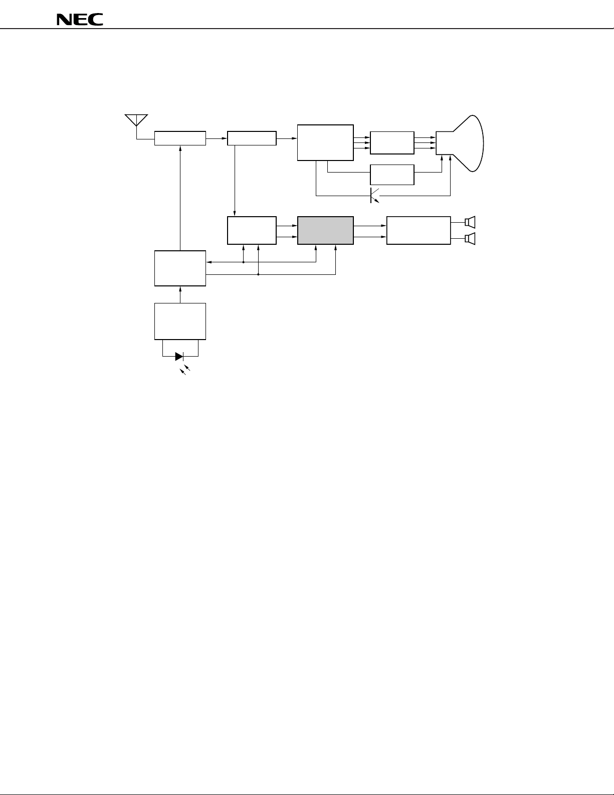
SYSTEM BLOCK DIAGRAM
•TV
µ
PC1853
µ
PD17002
µ
PD17052
µ
PD17053
µ
PC2800A
µ
PC2801A
Tuner PIF & SIF
Digital
tuning
controller
Remote control
reception
amplifier
PIN photo diode
SDA
SCL
µ
PC1852
US MTS
processor
Color, intensity
and deflecting
Signal processor
µ
PC1853
L
Surround
Surround
processor
processor
R
RGB
output
Vertical
output
µ
PC1310
µ
PC1316C
Power amplifier
CRT
2
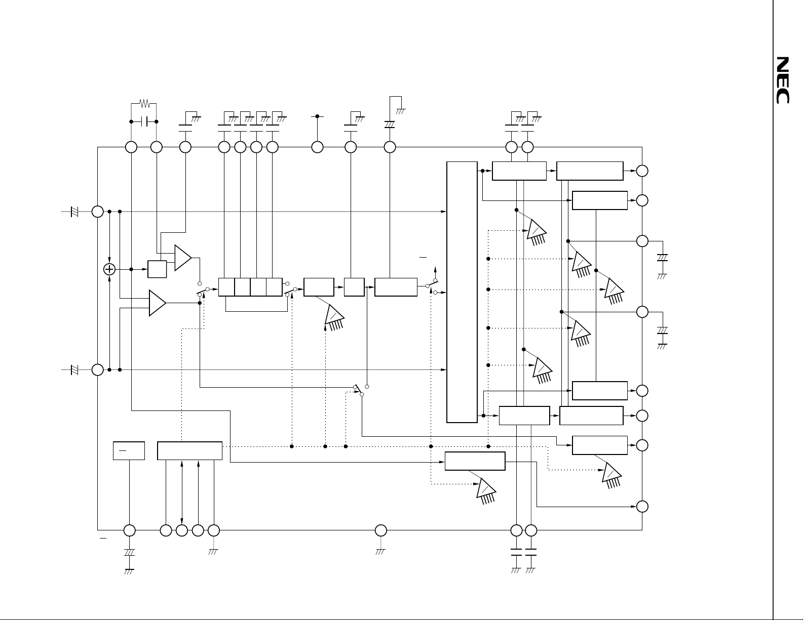
820 kΩ
0.022 F
µ
0.022 F
12 V
µ
CC
V
0.1 F
µ
2200 pF
FC1FC2 FC3 FC4
680 pF
0.082 F
µ
MFO MFI LF1
29 30 28 2 3 4 5 15 6 25
1000 pF
LF2 OFC
–
+
µ
22 F
0.1 F
µ
LBC LTC
10 9
6800 pF
BLOCK DIAGRAM
(1)
µ
PC1853-01
L
in
–+
22 F
µ
in
R
–+
22 F
µ
26
27
A
Bass
Treble
D
A
Volume, balance
control/Mute
Volume control
/Mute
D
A
Volume
Balance
D
Volume control
/Mute
Volume, balance
control/Mute
Volume control
/Mute
D
A
D
L1 OUT
14
L2 OUT
17
VOL-C
18
+
3.3 F
µ
–
A
BAL-C
19
+
µ
3.3 F
–
R2 OUT
16
13
R1 OUT
11
Rear OUT
A
µ
12
L+R OUT
PC1853
Tone control/
Low boost
D
–
+
LPF
–
+
1
V
2
CC
I2C bus interface
PS1PS2PS3 PS4
Phase shifter
Effect
control
LPF
D
A
Offset
absorption
1
V
2
CC
Matrix
L + R volume
control/Mute
D
A
Tone control/
Low boost
23
1
CC
V
2
3
µ
22 F
+
–
ADS SDA SCL
20212224
1
GNDGND
RBC RTC
0.1 F
7
8
µ
6800 pF
4
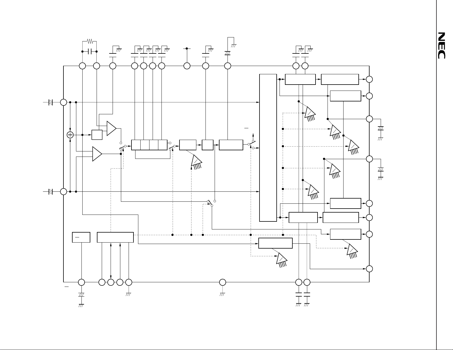
(2)
820 kΩ
µ
PC1853-02
0.082 F
µ
0.022 F
µ
0.022 F
12 V
µ
CC
V
0.1 F
µ
2200 pF
FC1FC2FC3 FC4
680 pF
MFIMFO LF1
3029 28 2 3 4 5 15 6 25
1000 pF
LF2 OFC
–
+
µ
22 F
0.1 F
µ
LBC LTC
10 9
6800 pF
L
in
–+
22 F
µ
in
R
–+
22 F
µ
26
27
A
Bass
Volume control
/Mute
Volume control
/Mute
D
A
D
A
L1 OUT
14
L2 OUT
17
LVC
18
+
3.3 F
µ
–
D
A
RVC
19
+
µ
3.3 F
–
LPF
–
+
Tone control
D
–
+
PS1PS2PS3PS4
Effect
control
LPF
Offset
absorption
1
V
CC
2
Matrix
Phase shifter
D
A
Treble
D
A
Volume control
/Mute
Tone control
1
V
2
CC
I2C bus interface
L + R volume
control/Mute
D
A
Volume control
/Mute
Volume control
/Mute
D
A
R2 OUT
16
13
R1 OUT
11
Rear OUT
12
L+R OUT
1
V
2
µ
22 F
23
CC
+
ADS SDA SCL
20212224
–
1
GNDGND
RBC RTC
µ
0.1 F
7
8
6800 pF
µ
PC1853

PIN CONFIGURATION (Top View)
(1)µPC1853-01
µ
PC1853
Ground (for Analog) Monaural filter inputGND MFI
Phase shift filter 1 Monaural filter outputFC1 MFO
Phase shift filter 2 Low-pass filter 1FC2 LF1
Phase shift filter 3 R-channel signal inputFC3 R
Phase shift filter 4 L-channel signal inputFC4 L
Low-pass filter 2 Offset absorption capacitorLF2 OFC
R-channel treble capacitor Reference voltage filterRTC V
R-channel bass capacitor Ground (for I2C bus)RBC GND
L-channel treble capacitor Slave address selectLTC ADS
L-channel bass capacitor Serial data (for I
Rear output Serial clock (for I
L+R signal output Balance offset absorption capacitorL+R OUT BAL-C
R-channel signal output 1 Volume offset absorption capacitorR1 OUT VOL-C
130
229
328
427
526
625
724
823
922
10 21
11 20
12 19
13 18
µ
PC1853CT –01
in
in
1
CC
2
2
C bus)LBC SDA
2
C bus)Rear OUT SCL
L-channel signal output 1 L-channel signal output 2L1 OUT L2 OUT
Power supply R-channel signal output 2V
14 17
15 16
CC
R2 OUT
5

(2)µPC1853-02
µ
PC1853
Ground (for Analog) Monaural filter inputGND MFI
Phase shift filter 1 Monaural filter outputFC1 MFO
Phase shift filter 2 Low-pass filter 1FC2 LF1
Phase shift filter 3 R-channel signal inputFC3 R
Phase shift filter 4 L-channel signal inputFC4 L
Low-pass filter 2 Offset absorption capacitorLF2 OFC
R-channel treble capacitor Reference voltage filterRTC V
R-channel bass capacitor Ground (for I2C bus)RBC GND
L-channel treble capacitor Slave address selectLTC ADS
L-channel bass capacitor Serial data (for I
Rear output Serial clock (for I
L+R signal output R-channel volume offset absorption capacitorL+R OUT RVC
R-channel signal output 1 L-channel volume offset absorption capacitorR1 OUT LVC
130
229
328
427
526
625
724
823
922
10 21
11 20
12 19
13 18
µ
PC1853CT –02
in
in
1
CC
2
2
C bus)LBC SDA
2
C bus)Rear OUT SCL
L-channel signal output 1 L-channel signal output 2L1 OUT L2 OUT
Power supply R-channel signal output 2V
14 17
15 16
CC
R2 OUT
6

µ
PC1853
CONTENTS
1. EXPLANATION OF PINS................................................................................................................ 8
2. ATTENTIONS.................................................................................................................................... 16
3. I2C BUS INTERFACE...................................................................................................................... 17
3.1 Data Transfer............................................................................................................................................. 17
3.1.1 Start condition .............................................................................................................................. 17
3.1.2 Stop condition............................................................................................................................... 18
3.1.3 Data transfer.................................................................................................................................. 18
3.2 Data Transfer Format ............................................................................................................................... 18
3.2.1 1 byte data transfer....................................................................................................................... 19
3.2.2 Serial data transfer ....................................................................................................................... 20
3.2.3 Acknowledge................................................................................................................................. 20
4. EXPLANATION OF EACH COMMAND......................................................................................... 21
4.1 Subaddress List........................................................................................................................................ 21
4.2 Initialization ............................................................................................................................................... 23
4.3 Surround Function ................................................................................................................................... 24
4.4 Explanation of Each Command............................................................................................................... 25
µ
4.4.1
4.4.2
PC1853-01 ................................................................................................................................... 25
µ
PC1853-02 ................................................................................................................................... 32
5. ELECTRICAL CHARACTERISTICS ............................................................................................... 35
6. CHARACTERISTIC CURVES.......................................................................................................... 63
6.1 Frequency Response Characteristics in Each Mode ............................................................................ 63
6.2 Characteristics of Phase Shifter and Rear Output ................................................................................ 66
6.3 Control Characteristics ............................................................................................................................ 68
6.4 Input/Output Characteristics, Distortion Rate ....................................................................................... 73
7. MEASURING CIRCUIT .................................................................................................................... 74
8. PACKAGE DIMENSIONS ................................................................................................................ 75
7
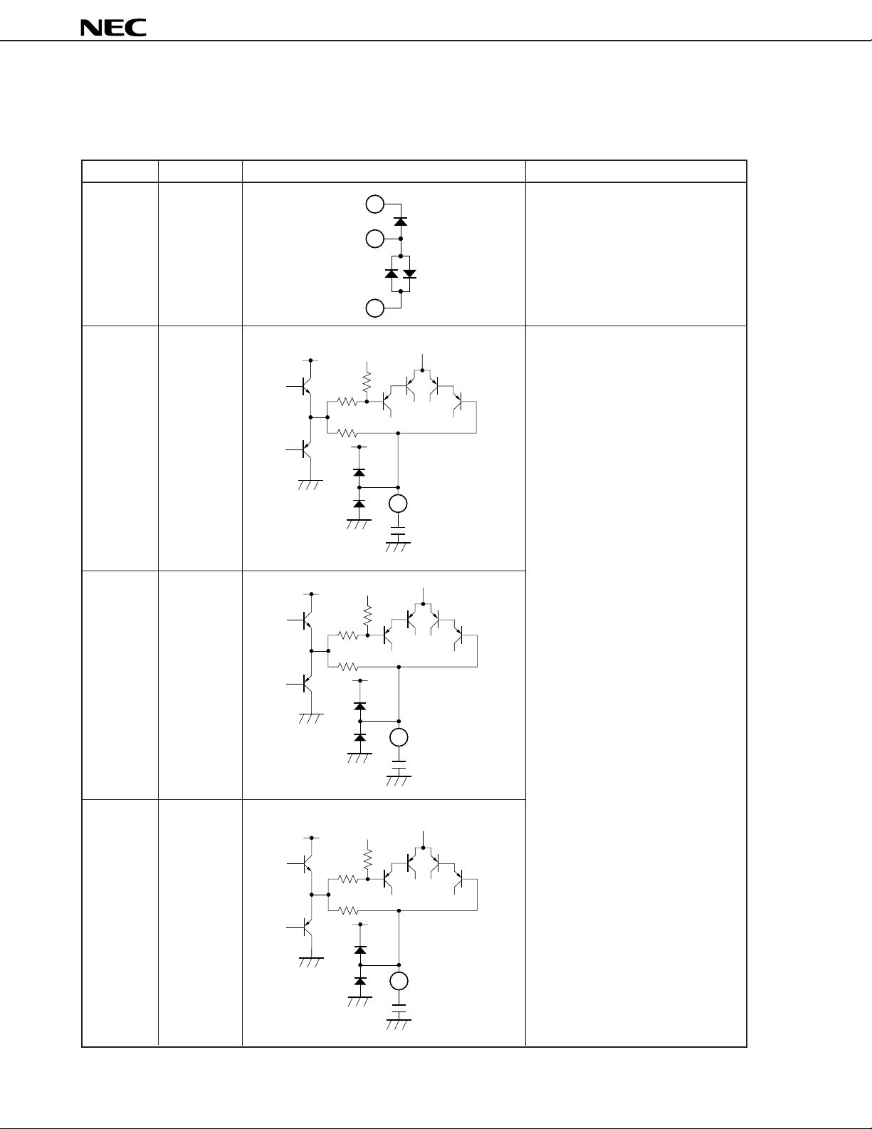
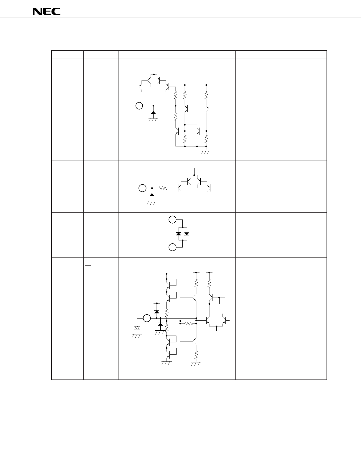
1. EXPLANATION OF PINS
Table 1-1 Explanation of Pins (1/8)
Pin Number Pin Name Equivalent Circuit Description
1 GND Ground for analog signal.
15
23
Pin voltage: approx. 0.0 V
1
µ
PC1853
2 FC1 Capacitor connection pin which
V
CC
36 kΩ
36 kΩ
determines time constant of phase
shifter.
Pin voltage: approx. 6.0 V
18 kΩ
V
CC
2
µ
F0.1
3 FC2
CC
V
36 kΩ
36 kΩ
18 kΩ
V
CC
3
8
4 FC3
2200 pF
V
CC
36 kΩ
36 kΩ
18 kΩ
V
CC
4
µ
F0.022
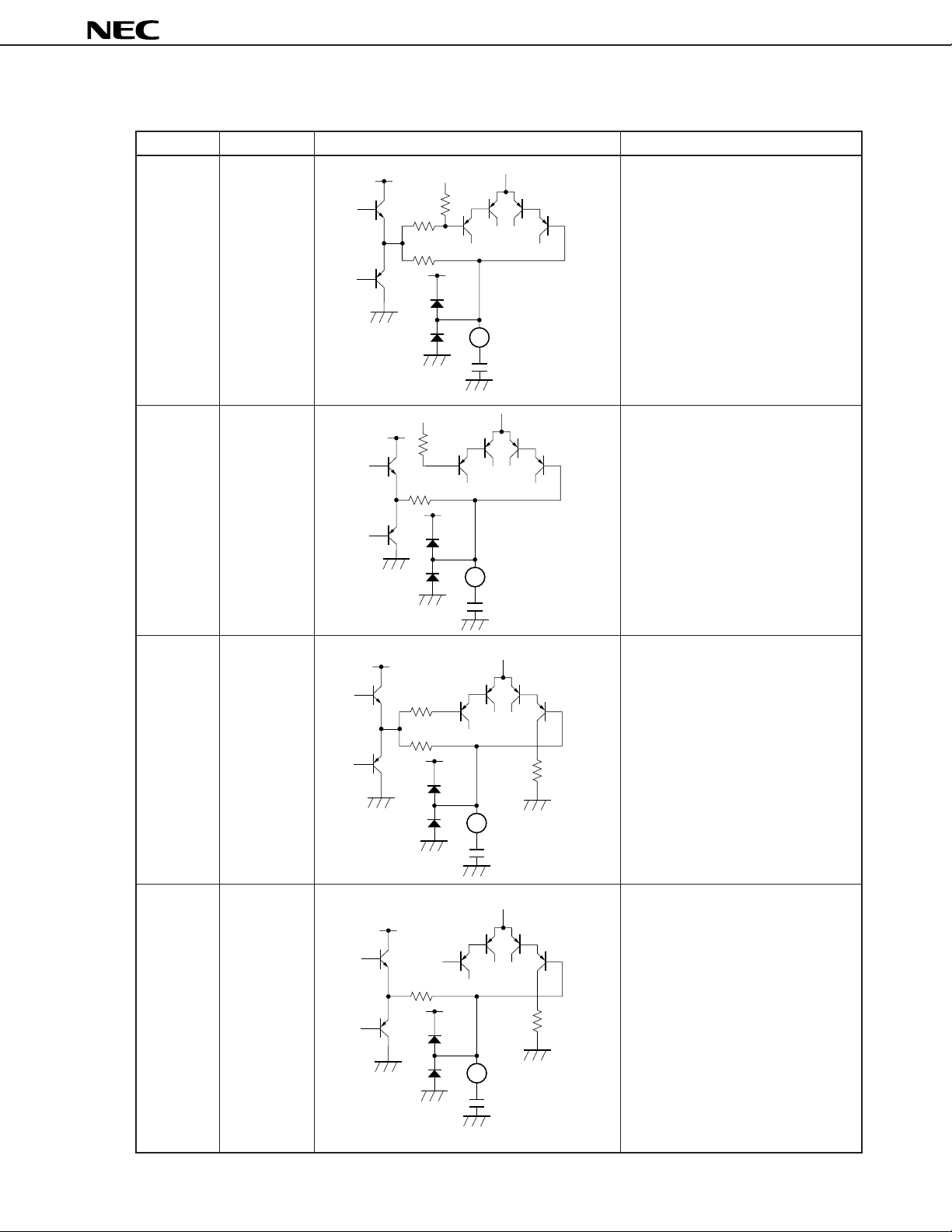
Table 1-1 Explanation of Pins (2/8)
Pin Number Pin Name Equivalent Circuit Description
5 FC4 Capacitor connection pin which
V
CC
36 kΩ
36 kΩ
determines time constant of phase
shifter.
Pin voltage: approx. 6.0 V
18 kΩ
V
CC
5
µ
F0.022
µ
PC1853
6 LF2 Low-pass filter.
CC
V
17.7 kΩ
Pin voltage: approx. 6.0 V
17.7 kΩ
V
CC
6
1000 pF
7 RTC Capacitor connection pin for treble
CC
V
boost/cut frequency characteristic of
R-channel signal.
7.5 kΩ
Pin voltage: approx. 6.0 V
5.8 kΩ
V
CC
3 kΩ
7
6800 pF
8 RBC Capacitor connection pin for bass
CC
V
boost/cut frequency characteristic of Rchannel signal.
Pin voltage: approx. 6.0 V
6.5 kΩ
VCC
3 kΩ
8
µ
F0.1
9
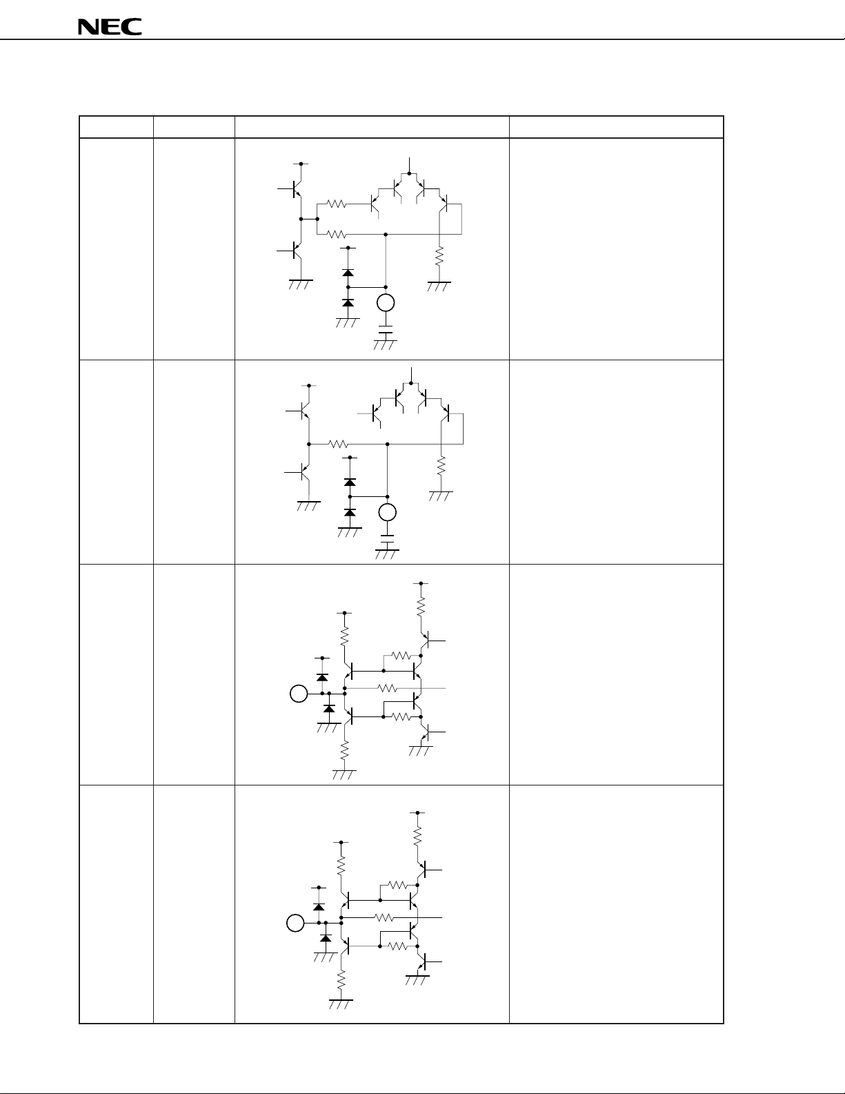
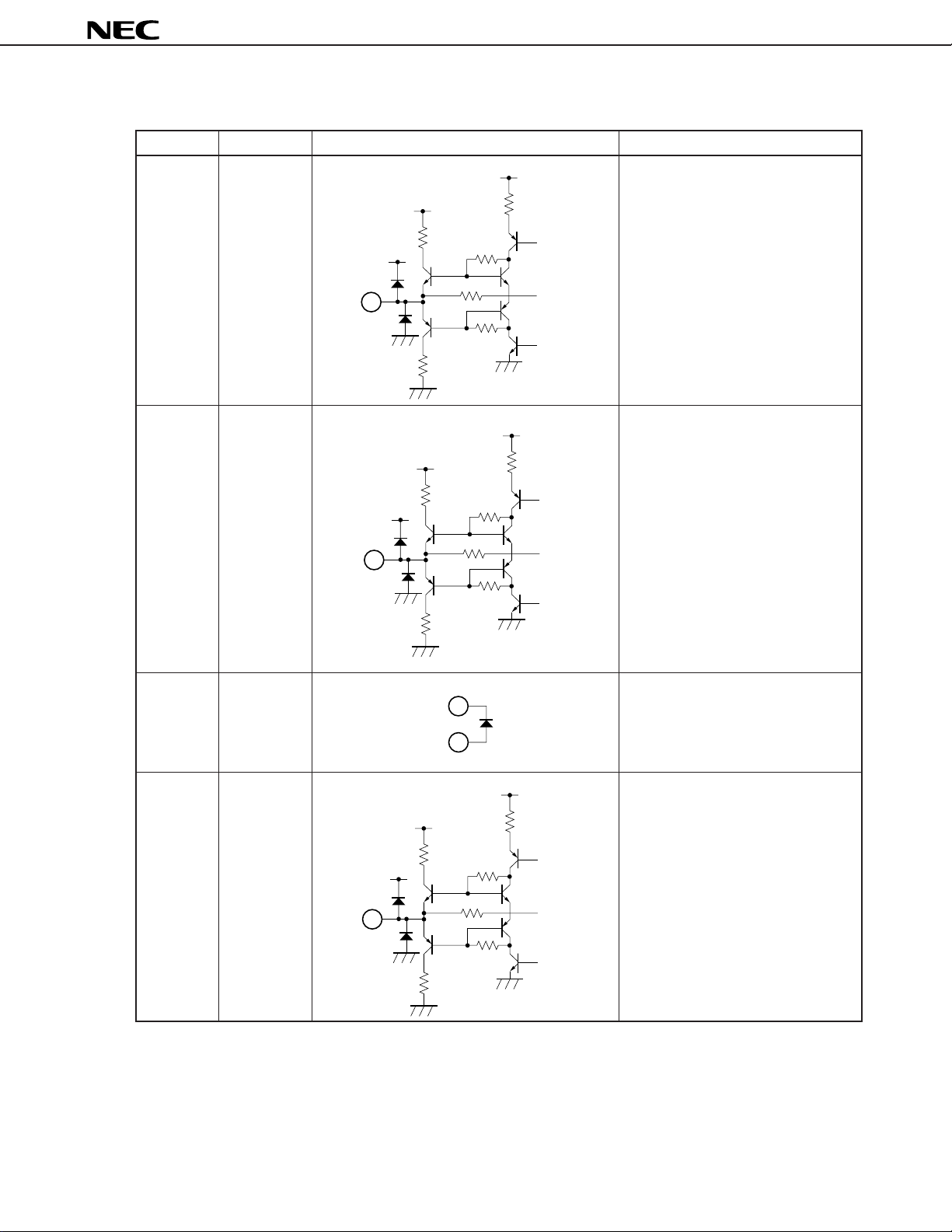
Table 1-1 Explanation of Pins (3/8)
Pin Number Pin Name Equivalent Circuit Description
9 LTC Capacitor connection pin for treble
CC
V
boost/cut frequency characteristic of
7.5 kΩ
L-channel signal.
Pin voltage: approx. 6.0 V
5.8 kΩ
V
CC
3 kΩ
9
pF6800
µ
PC1853
10 LBC Capacitor connection pin for bass
CC
V
boost/cut frequency characteristic of
L-channel signal.
6.5 kΩ
V
CC
3 kΩ
Pin voltage: approx. 6.0 V
10
µ
F0.1
V
4 kΩ
CC
500 Ω
output signal (φ(L-R) signal or (L-R)
signal) (see 4.4.1(4) or 4.4.2(2) Rear
output selection).
• φ(L-R): Phase-shifted.
• (L-R) : Not phase-shifted.
Pin voltage: approx. 6.0 V
11 Rear OUT L-R signal output pin. Select the
V
CC
4 kΩ
V
CC
15 kΩ
11
4 kΩ
4 kΩ
12 L+R OUT L+R signal output pin.
V
CC
4 kΩ
V
CC
4 kΩ
V
CC
Pin voltage: approx. 6.0 V
500 Ω
15 kΩ
12
4 kΩ
4 kΩ
10
µ
Table 1-1 Explanation of Pins (4/8)
Pin Number Pin Name Equivalent Circuit Description
V
4 kΩ
4 kΩ
CC
500 Ω
output).
Pin voltage: approx. 6.0 V
13 R1 OUT R-channel signal output pin (for main
V
CC
4 kΩ
V
CC
15 kΩ
13
4 kΩ
PC1853
14 L1 OUT L-channel signal output pin (for main
V
CC
4 kΩ
V
CC
4 kΩ
V
CC
500 Ω
output).
Pin voltage: approx. 6.0 V
15 kΩ
14
4 kΩ
4 kΩ
15 VCC Supply voltage.
15
Pin voltage: approx. 12.0 V
1
V
16 R2 OUT R-channel signal output pin for
CC
external audio processor and so on.
V
CC
4 kΩ
V
CC
4 kΩ
500 Ω
Pin voltage: approx. 6.0 V
16
15 kΩ
4 kΩ
4 kΩ
11
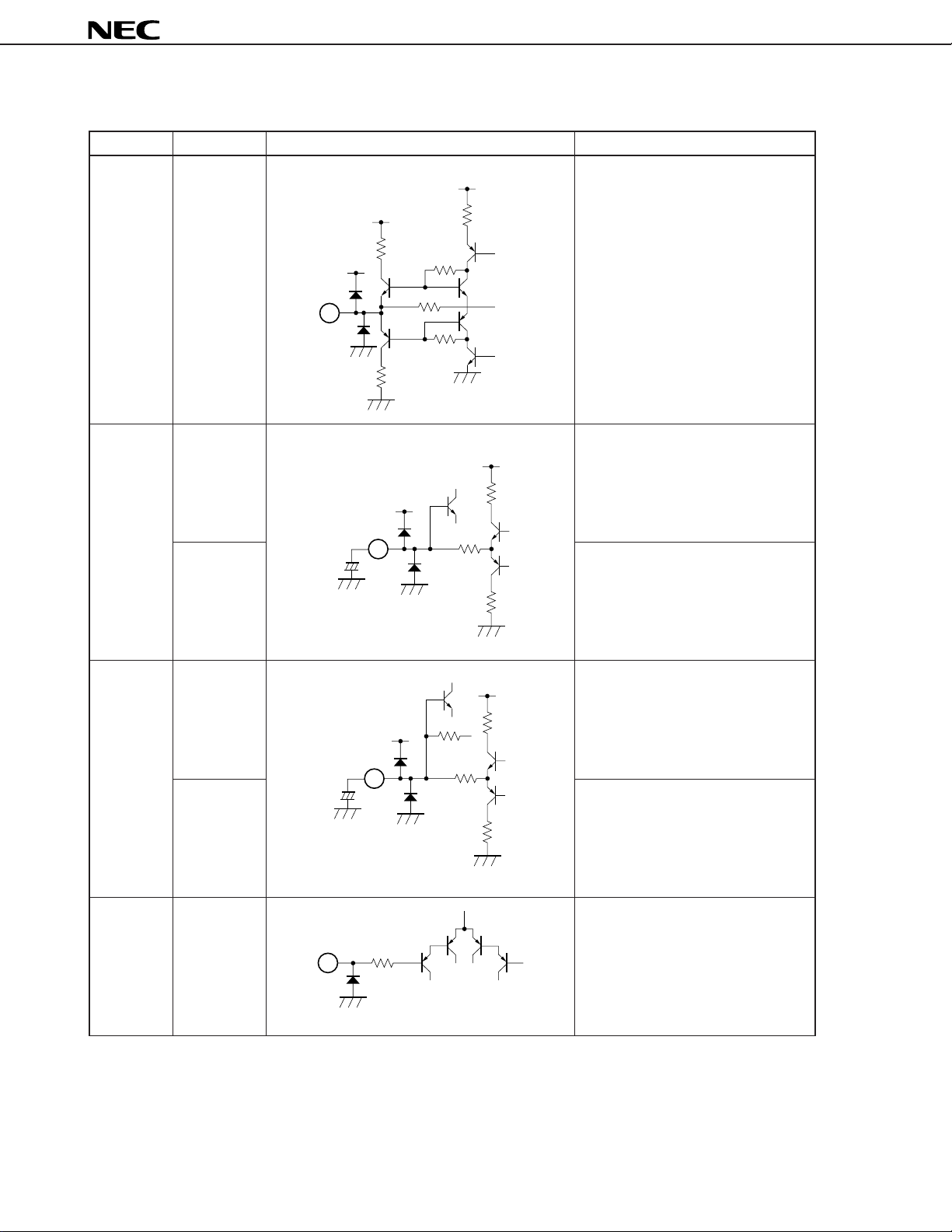
Table 1-1 Explanation of Pins (5/8)
Pin Number Pin Name Equivalent Circuit Description
17 L2 OUT L-channel signal output pin for external
VCC
4 kΩ
VCC
17
4 kΩ
18 VOL-C Capacitor connection pin which
(µPC1853-01) absorbs shock noise of D/A converter
CC
V
15 kΩ
4 kΩ
4 kΩ
VCC
500 Ω
V
CC
4 kΩ
audio processor and so on.
Pin voltage: approx. 6.0 V
for volume control.
Pin voltage: approx. 6.0 V
µ
PC1853
15 kΩ
500 Ω
500 Ω
4 kΩ
V
CC
4 kΩ
4 kΩ
for L-channel volume control.
Pin voltage: approx. 6.0 V
for balance control.
Pin voltage: approx. 4.8 V
for R-channel volume control.
Pin voltage: approx. 4.8 V
bus).
Pin voltage: approx. 0.0 V
18
µ
20
+
µ
F3.3
CC
V
19
+
F3.3
4 kΩ
LVC Capacitor connection pin which
(µPC1853-02) absorbs shock noise of D/A converter
19 BAL-C Capacitor connection pin which
(µPC1853-01) absorbs shock noise of D/A converter
RVC Capacitor connection pin which
(µPC1853-02) absorbs shock noise of D/A converter
20 SCL Serial clock line pin (clock input for I2C
12
µ
Table 1-1 Explanation of Pins (6/8)
Pin Number Pin Name Equivalent Circuit Description
21 SDA Serial data line pin (data input for I2C
bus).
Pin voltage: approx. 0.0 V
21
4 k
150 Ω
Ω
CC
V
1 kΩ 1 kΩ
V
CC
PC1853
25
kΩ
125 kΩ
22 ADS Slave address selection pin.
Pin voltage: approx. 0.0 V
22
23 DGND Ground for I2C bus signal.
4 kΩ
1
Pin voltage: approx. 0.0 V
23
24 1
2 voltage.
VCC
V
CC
CC
V
V
CC
Filter pin for middle point of supply
Pin voltage: approx. 6.0 V
10 kΩ5 kΩ
V
CC
24
+
µ
F22
20 kΩ
10 kΩ
5 kΩ
13
20 kΩ
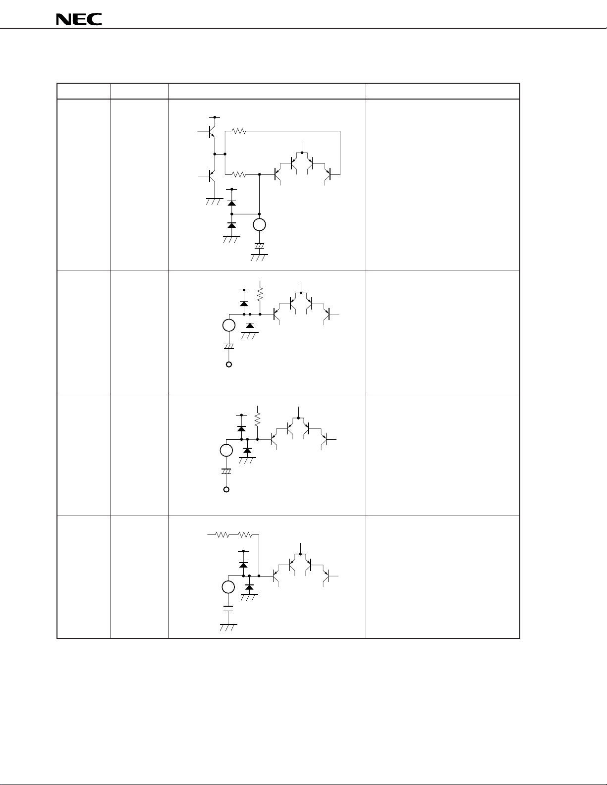
Table 1-1 Explanation of Pins (7/8)
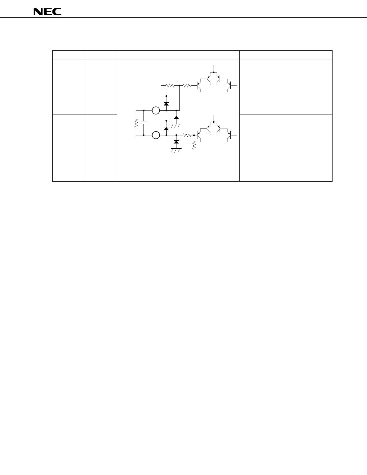
Pin Number Pin Name Equivalent Circuit Description
25 OFC Capacitor connection pin which
VCC
10 kΩ
10 kΩ
VCC
25
absorbs offset voltage generated by
phase shifter.
Pin voltage: approx. 6.0 V
+
µ
F22
µ
PC1853
26 Lin L-channel signal input pin.
27 Rin R-channel signal input pin.
signal input
28 LF1 Low-pass filter.
26
+
µ
F22
L-channel
signal input
V
27
+
µ
F22
R-channel
18 kΩ
1 kΩ
VCC
V
CC
60 kΩ
CC
60 kΩ
Input impedance: 60 kΩ
Pin voltage: approx. 6.0 V
Input impedance: 60 kΩ
Pin voltage: approx. 6.0 V
Pin voltage: approx. 6.0 V
14
28
680 pF
µ
PC1853
Table 1-1 Explanation of Pins (8/8)
Pin Number Pin Name Equivalent Circuit Description
29 MFO High-pass filter output pin for surround
function (Simulated mode)
18 kΩ1 kΩ
V
CC
(see 4.3 Surround Function).
Pin voltage: approx. 6.0 V
30 MFI High-pass filter input pin for surround
820 kΩ
29
0.082 F
µ
30
V
CC
15 kΩ
47 kΩ
function (Simulated mode)
(see 4.3 Surround Function).
Pin voltage: approx. 6.0 V
15

2. ATTENTIONS
<1> Attention on Pop Noise Reduction
When changing the surround mode and switching power, use the mute function (approx. 200 ms) for pop noise
reduction (see 4.4.1(2) Mute for the µPC1853-01 or 4.4.2(1) Mute for the µPC1853-02).
<2> Attention on Supply Voltage
2
Drive data on the I
C bus after supply voltage of total application system becomes stable.
µ
PC1853
16
µ
PC1853
3. I2C BUS INTERFACE
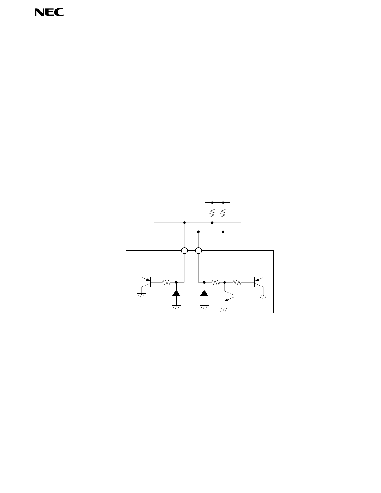
The µPC1853 has serial bus function. This serial bus (I2C bus) is a double wired bus developed by Philips. It is
composed of 2 wires: serial clock line (SCL) and serial data line (SDA).
The µPC1853 has built-in I2C bus interface circuit, 9 rewritable registers (8 bits).
SCL (Serial Clock Line)
µ
The master CPU outputs serial clock to synchronize with the data. According to this clock, the
in the serial data.
Input level is compatible with CMOS.
Clock frequency is 0 to 100 kHz.
SDA (Serial Data Line)
µ
The master CPU outputs the data which is synchronized with serial clock. The
PC1853 takes in this data according
to the clock.
Input level is compatible with CMOS.
Fig. 3-1 Internal Equivalent Circuits of Interface Pin
PC1853 takes
SCL
SDA
R
PC1853
µ
P
R
P
3.1 Data Transfer
3.1.1 Start condition
Start condition is made by falling of SDA from “High” to “Low” during SCL is “High” as shown in Fig. 3-2.
When this start condition is received, the
µ
PC1853 takes in the data synchronizing with the clock after that.
17

3.1.2 Stop condition
Stop condition is made by rising of SDA from “Low” to “High” during SCL is “High” as shown in Fig. 3-2.
When this stop condition is received, the
µ
PC1853 stops to take in or output the data.
Fig. 3-2 Start/Stop Condition of Data Transfer
3.5 V
SDA
1.5 V
MIN.
3.5 V
µ
s4.0
MIN.
µ
s4.7
µ
PC1853
SCL
START
1.5 V
STOP
3.1.3 Data transfer
In the case of data transfer, data changing should be executed while SCL is “Low” like Fig. 3-3. When SCL is “High”,
be sure not to change the data.
Fig. 3-3 Data Transfer
SDA
Note 1 Note 2
SCL
Note 1. Data hold time for I2C device: 300 ns MIN., Data hold time for CPU: 5 µs MIN.
2. Data set-up time: 250 ns MIN.
Remark Clock frequency: 0 to 100 kHz
3.2 Data Transfer Format
Fig. 3-4 is an example of data transfer in write mode.
18
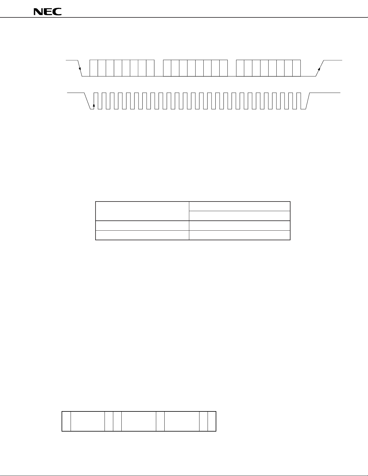
Fig. 3-4 Example of Data Transfer in Write Mode
µ
PC1853
SDA
SCL
Slave address
D6 D5 D4 D3 D2 D1 D0 W
D7 D6 D5 D4 D3 D2 D1 D0D7
ACK
Subaddress
D6 D5 D4 D3 D2 D1 D0
ACK
Data
ACK
Remark W: Write mode, ACK: Acknowledge bit
Data is composed of 8 bits. Acknowledge bit is always added after this 8 bits data. Data should be transferred
from MSB first.
The 1 byte immediately after start condition specifies the slave address (chip address). This slave address is
composed of 7 bits.
µ
Table 3-1 is the slave address of the
PC1853. This slave address is registered by Phillips.
Table 3-1 Slave Address of µPC1853
Bias Voltage of ADS (Pin 22)
5V 1000110
GND 1000100
D6 D5 D4 D3 D2 D1 D0
Slave address
User can set bit D1 freely.
0: Bias voltage of ADS (pin 22) is GND.
1: Bias voltage of ADS (pin 22) is 5 V.
The remaining 1 bit is the read/write bit which specifies the direction of the data transferred after that. Set “0”
µ
because the
PC1853 has write mode only.
The byte following the slave address is subaddress byte of the µPC1853.
µ
PC1853 has 9 subaddresses from SA0 to SA8, and each of them is composed of 8 bits. The data to be set
The
to the subaddress follows this subaddress byte.
µ
PC1853 has automatic increment function. This function increments subaddress automatically in write mode.
The
By using automatic increment function, once slave address and subaddress are set, data can be transferred
continuously to the next subaddress. Use this function for initializing and so on. In the case of changing the data
continuously of one subaddress (adjustment and so on), set the automatic increment function OFF (see 4.4.1(8)
Automatic increment function).
3.2.1 1 byte data transfer
The following is the format in the case of transferring 1 byte data.
S
T
A
SLAVE
ADDRESS
A
C
K
SUB
ADDRESS
W
A
DATA
C
K
A
S
C
T
K
P
Remark STA: Start, W: Write mode, ACK: Acknowledge bit, STP: Stop
19

3.2.2 Serial data transfer
The following is the format in the case of transferring 8 bytes data at one time by using automatic increment function
(the data of subaddress 01H to 08H, bit D6 is “1”).
µ
PC1853
S
T
A
SLAVE
ADDRESS
A
C
K
SUB
ADDRESS
W
A
C
DATA1 DATA2 DATA9
K
A
C
K
A
C
K
A
S
C
T
K
P
Remark STA: Start, W: Write mode, ACK: Acknowledge, STP: Stop
The master CPU transfers “00H” as subaddress SA
0 after start and slave address like above figure. It transfers
the data of SA0 after subaddress, and then transfers the data of SA1, SA2..., SA8 continuously without transferring
stop condition. Finally, it transfers stop condition and terminates.
µ
The increments of the subaddress of the
PC1853 stops automatically when the subaddress comes to “08H” inside
of it.
3.2.3 Acknowledge
2
On I
C bus, acknowledge bit is added to the 9th bit after the data in order to judge whether data transfer has been
succeeded or not. The master CPU judges it from “High” and “Low” of acknowledge condition.
When this acknowledge period is “Low”, it means success. And when the condition is “High”, it means failure of
transfer or forced release of bus as NAK state.
The condition of being NAK state is when wrong slave address is transferred to slave IC or data transfer from slave
side is finished in read state.
20

(1) µPC1853-01
4. EXPLANATION OF EACH COMMAND
4.1 Subaddress List
21
Bit
Subaddress
00H Rear output Low boost Low boost gain Rear output L+R signal Audio output Main output Audio output
01H 0 Automatic increment Main output volume control
02H 0 Automatic increment Balance control
03H 0 Automatic increment Bass control
04H 0 Automatic increment Treble control
05H 0 Automatic increment L+R signal output volume control
06H 0 Automatic increment Audio output volume control
07H 0 Automatic increment Rear output volume control
08H Surround Automatic increment Units of phase
MSB LSB
D7
selection 0: OFF 0: 6 dB mute output mute mute mute control link
0:
φ
(L-R) 1: ON 1: 3 dB 0: OFF 0: OFF 0: OFF 0: OFF 0: OFF
1: L-R 1: ON 1: ON 1: ON 1: ON 1: ON
0: OFF Attenuation volume : Flat to Low
1: ON Data : 111111 to 000000
0: OFF L-channel attenuation volume : Low to Flat to Flat
1: ON R-channel attenuation volume : Flat to Flat to Low
0: OFF Gain : Boost to 0 dB to Cut
1: ON Data : 111111 to 100000 to 000000
0: OFF Gain : Boost to 0 dB to Cut
1: ON Data : 111111 to 100000 to 000000
0: OFF Attenuation volume : Flat to Low
1: ON Data : 111111 to 000000
0: OFF Attenuation volume : Flat to Low
1: ON Data : 111111 to 000000
0: OFF Attenuation volume : Flat to Low
1: ON Data : 111111 to 000000
ON/OFF 0: OFF shifters selection Effect : Large to Normal to Small
OFF 1: ON 0: 4 units 0: Stereo Data : 1111 to 1000 to 0000
0:
1: ON 1: 1 unit 1: Monaural
D6 D5 D4 D3 D2 D1
Data : 111111 to 100000 to 000000
Monaural/Stereo
Effect control
D0
µ
PC1853
Caution Be sure to write data “0” in the subaddress 01H to 07H, bit D7.

22
(2)
µ
PC1853-02
Bit
Subaddress
00H Rear output 0 0 Rear output L+R signal Audio output 0 0
01H 0 Automatic increment R-channel signal output (R1 OUT pin) volume control
02H 0 Automatic increment L-channel signal output (L1 OUT pin) volume control
03H 0 Automatic increment Bass control
04H 0 Automatic increment Treble control
05H 0 Automatic increment L+R signal output volume control
06H 0 Automatic increment Audio output volume control
07H 0 Automatic increment Rear output volume control
08H Surround Automatic increment Units of phase
MSB LSB
D7
selection mute output mute mute
0:
φ
(L-R) 0: OFF 0: OFF 0: OFF
1: L-R 1: ON 1: ON 1: ON
0: OFF Attenuation volume : Flat to Low
1: ON Data : 111111 to 000000
0: OFF Attenuation volume : Flat to Low
1: ON Data : 111111 to 000000
0: OFF Gain : Boost to 0 dB to Cut
1: ON Data : 111111 to 100000 to 000000
0: OFF Gain : Boost to 0 dB to Cut
1: ON Data : 111111 to 100000 to 000000
0: OFF Attenuation volume : Flat to Low
1: ON Data : 111111 to 000000
0: OFF Attenuation volume : Flat to Low
1: ON Data : 111111 to 000000
0: OFF Attenuation volume : Flat to Low
1: ON Data : 111111 to 000000
ON/OFF 0: OFF shifters selection Effect : Large to Normal to Small
OFF 1: ON 0: 4 units 0: Stereo Data : 1111 to 1000 to 0000
0:
1: ON 1: 1 unit 1: Monaural
D6 D5 D4 D3 D2 D1
Monaural/Stereo
Effect control
D0
µ
PC1853
Caution Be sure to fix data of the subaddress 00H, bit D6, D5, D1, D0 and subaddress 01H to 07H, bit D7 to “0”.
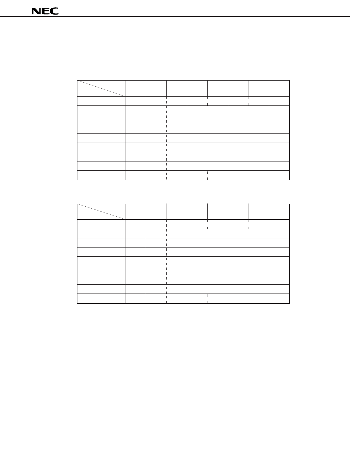
4.2 Initialization
After power-on, be sure to initialize the subaddress data to table below.
Table 4-1 Initial Data of µPC1853-01
Bit MSB LSB
Subaddress D7 D6 D5 D4 D3 D2 D1 D0
00H 10000000
01H 01111111
02H 01100000
03H 01100000
04H 01100000
05H 01111111
06H 01111111
07H 01111111
08H 01001000
µ
PC1853
Table 4-2 Initial Data of µPC1853-02
Bit MSB LSB
Subaddress D7 D6 D5 D4 D3 D2 D1 D0
00H 10000000
01H 01111111
02H 01111111
03H 01100000
04H 01100000
05H 01111111
06H 01111111
07H 01111111
08H 01001000
Caution Until initializing completely, mute by the external units.
23
 Loading...