

Page 1

User’s Manual
µ
PD789489 Subseries
8-Bit Single-Chip Microcontrollers
µ
PD789488
µ
PD789489
µ
PD78F9488
µ
PD78F9489
Document No. U15331EJ4V1UD00 (4th edition)
Date Published July 2005 NS CP(K)
©
Printed in Japan
Page 2

[MEMO]
2 User’s Manual U15331EJ4V1UD
Page 3
NOTES FOR CMOS DEVICES
1
VOLTAGE APPLICATION WAVEFORM AT INPUT PIN
Waveform distor tion due to input noise or a reflected wave may cause malfunction. If the input of the
CMOS device stays in the area between V
malfunction. Take care to prevent chattering noise from entering the device when the input level is fixed,
and also in the transition period when the input level passes through the area between V
IH (MIN).
V
HANDLING OF UNUSED INPUT PINS
2
Unconnected CMOS device inputs can be cause of malfunction. If an input pin is unconnected, it is
possible that an internal input level may be generated due to noise, etc., causing malfunction. CMOS
devices behave differently than Bipolar or NMOS devices. Input levels of CMOS devices must be fixed
high or low by using pull-up or pull-down circuitry. Each unused pin should be connected to V
via a resistor if there is a possibility that it will be an output pin. All handling related to unused pins must
be judged separately for each device and according to related specifications governing the device.
3
PRECAUTION AGAINST ESD
A strong electric field, when exposed to a MOS device, can cause destruction of the gate oxide and
ultimately degrade the device operation. Steps must be taken to stop generation of static electricity as
much as possible, and quickly dissipate it when it has occurred. Environmental control must be
adequate. When it is dry, a humidifier should be used. It is recommended to avoid using insulators that
easily build up static electricity. Semiconductor devices must be stored and transported in an anti-static
container, static shielding bag or conductive material. All test and measurement tools including work
benches and floors should be grounded. The operator should be grounded using a wrist strap.
Semiconductor devices must not be touched with bare hands. Similar precautions need to be taken for
PW boards with mounted semiconductor devices.
IL (MAX) and VIH (MIN) due to noise, etc., the device may
IL (MAX) and
DD or GND
4
STATUS BEFORE INITIALIZATION
Power-on does not necessarily define the initial status of a MOS device. Immediately after the power
source is turned ON, devices with reset functions have not yet been initialized. Hence, power-on does
not guarantee output pin levels, I/O settings or contents of registers. A device is not initialized until the
reset signal is received. A reset operation must be executed immediately after power-on for devices
with reset functions.
5
POWER ON/OFF SEQUENCE
In the case of a device that uses different power supplies for the internal operation and external
interface, as a rule, switch on the external power supply after switching on the internal power supply.
When switching the power supply off, as a rule, switch off the external power supply and then the
internal power supply. Use of the reverse power on/off sequences may result in the application of an
overvoltage to the internal elements of the device, causing malfunction and degradation of internal
elements due to the passage of an abnormal current.
The correct power on/off sequence must be judged separately for each device and according to related
specifications governing the device.
6
INPUT OF SIGNAL DURING POWER OFF STATE
Do not input signals or an I/O pull-up power supply while the device is not powered. The current
injection that results from input of such a signal or I/O pull-up power supply may cause malfunction and
the abnormal current that passes in the device at this time may cause degradation of internal elements.
Input of signals during the power off state must be judged separately for each device and according to
related specifications governing the device.
User’s Manual U15331EJ4V1UD 3
Page 4

EEPROM and FIP are trademarks of NEC Electronics Corporation.
Windows and Windows NT are either registered trademarks or trademarks of Microsoft Corporation in the
United States and/or other countries.
PC/AT is a trademark of International Business Machines Corporation.
HP9000 series 700 and HP-UX are trademarks of Hewlett-Packard Company.
SPARCstation is a trademark of SPARC International, Inc.
Solaris and SunOS are trademarks of Sun Microsystems, Inc.
These commodities, technology or software, must be exported in accordance
with the export administration regulations of the exporting country.
Diversion contrary to the law of that country is prohibited.
4 User’s Manual U15331EJ4V1UD
Page 5

•
The information in this document is current as of July, 2005. The information is subject to change
without notice. For actual design-in, refer to the latest publications of NEC Electronics data sheets or
data books, etc., for the most up-to-date specifications of NEC Electronics products. Not all
products and/or types are available in every country. Please check with an NEC Electronics sales
representative for availability and additional information.
No part of this document may be copied or reproduced in any form or by any means without the prior
•
written consent of NEC Electronics. NEC Electronics assumes no responsibility for any errors that may
appear in this document.
•
NEC Electronics does not assume any liability for infringement of patents, copyrights or other intellectual
property rights of third parties by or arising from the use of NEC Electronics products listed in this document
or any other liability arising from the use of such products. No license, express, implied or otherwise, is
granted under any patents, copyrights or other intellectual property rights of NEC Electronics or others.
Descriptions of circuits, software and other related information in this document are provided for illustrative
•
purposes in semiconductor product operation and application examples. The incorporation of these
circuits, software and information in the design of a customer's equipment shall be done under the full
responsibility of the customer. NEC Electronics assumes no responsibility for any losses incurred by
customers or third parties arising from the use of these circuits, software and information.
•
While NEC Electronics endeavors to enhance the quality, reliability and safety of NEC Electronics products,
customers agree and acknowledge that the possibility of defects thereof cannot be eliminated entirely. To
minimize risks of damage to property or injury (including death) to persons arising from defects in NEC
Electronics products, customers must incorporate sufficient safety measures in their design, such as
redundancy, fire-containment and anti-failure features.
•
NEC Electronics products are classified into the following three quality grades: "Standard", "Special" and
"Specific".
The "Specific" quality grade applies only to NEC Electronics products developed based on a customerdesignated "quality assurance program" for a specific application. The recommended applications of an NEC
Electronics product depend on its quality grade, as indicated below. Customers must check the quality grade of
each NEC Electronics product before using it in a particular application.
"Standard":
"Special":
"Specific":
Computers, office equipment, communications equipment, test and measurement equipment, audio
and visual equipment, home electronic appliances, machine tools, personal electronic equipment
and industrial robots.
Transportation equipment (automobiles, trains, ships, etc.), traffic control systems, anti-disaster
systems, anti-crime systems, safety equipment and medical equipment (not specifically designed
for life support).
Aircraft, aerospace equipment, submersible repeaters, nuclear reactor control systems, life
support systems and medical equipment for life support, etc.
The quality grade of NEC Electronics products is "Standard" unless otherwise expressly specified in NEC
Electronics data sheets or data books, etc. If customers wish to use NEC Electronics products in applications
not intended by NEC Electronics, they must contact an NEC Electronics sales representative in advance to
determine NEC Electronics' willingness to support a given application.
(Note)
(1)
"NEC Electronics" as used in this statement means NEC Electronics Corporation and also includes its
majority-owned subsidiaries.
(2)
"NEC Electronics products" means any product developed or manufactured by or for NEC Electronics (as
defined above).
M8E 02. 11-1
User’s Manual U15331EJ4V1UD 5
Page 6

Regional Information
Some information contained in this document may vary from country to country. Before using any NEC
Electronics product in your application, pIease contact the NEC Electronics office in your country to
obtain a list of authorized representatives and distributors. They will verify:
•
Device availability
•
Ordering information
•
Product release schedule
•
Availability of related technical literature
•
Development environment specifications (for example, specifications for third-party tools and
components, host computers, power plugs, AC supply voltages, and so forth)
•
Network requirements
In addition, trademarks, registered trademarks, export restrictions, and other legal issues may also vary
from country to country.
[GLOBAL SUPPORT]
http://www.necel.com/en/support/support.html
NEC Electronics America, Inc. (U.S.)
Santa Clara, California
Tel: 408-588-6000
800-366-9782
N
EC Electronics (Europe) GmbH
Duesseldorf, Germany
Tel: 0211-65030
•
Sucursal en España
Madrid, Spain
Tel: 091-504 27 87
•
Succursale Française
Vélizy-Villacoublay, France
Tel: 01-30-67 58 00
•
Filiale Italiana
Milano, Italy
Tel: 02-66 75 41
•
Branch The Netherlands
Eindhoven, The Netherlands
Tel: 040-265 40 10
•
Tyskland Filial
Taeby, Sweden
Tel: 08-63 87 200
•
United Kingdom Branch
Milton Keynes, UK
Tel: 01908-691-133
NEC Electronics Hong Kong Ltd.
Hong Kong
Tel: 2886-9318
NEC Electronics Hong Kong Ltd.
Seoul Branch
Seoul, Korea
Tel: 02-558-3737
NEC Electronics Shanghai Ltd.
Shanghai, P.R. China
Tel: 021-5888-5400
NEC Electronics Taiwan Ltd.
Taipei, Taiwan
Tel: 02-2719-2377
NEC Electronics Singapore Pte. Ltd.
Novena Square, Singapore
Tel: 6253-8311
6 User’s Manual U15331EJ4V1UD
J05.6
Page 7
Major Revisions in This Edition
Page Description
Throughout Change of descriptions of µPD789489, 78F9489
• Change of status from under development to development completed
• Change of the subseries name to “
pp.31 to 33 Update of 1.5 78K/0S Series Lineup to latest version
p.123 Modification of Figure 7-2 Block Diagram of Timer 50
p.124 Modification of Figure 7-3 Block Diagram of Timer 60
Modification of Figure 7-5 Block Diagram of Output control circuit (Timer 60) p.126
Addition of descriptions in 7.2 (2) 8-bit compare register 60
p.127 Addition of descriptions in 7.2 (4) 8-bit H width compare registers 60 and 61
p.136 Modification of Figure 7-11 8-bit Timing of Interval Timer Operation with 8-Bit Resolution (Basic Operation)
p.137 Modification of Figure 7-13. Timing of Interval Timer Operation with 8-Bit Resolution (When CRnm Is Set to
FFH)
p.140 Modification of Figure 7-17. Timing of Operation of External Event Counter with 8-Bit Resolution
p.150 Addition of descriptions of setting sequence in 7.4.3 Operation as carrier generator
p.151 Modification of Figure 7-22. Timing of Carrier Generator Operation (When CR60 = N, CRH60 = M (M > N))
p.152 Modification of Figure 7-23. Timing of Carrier Generator Operation (When CR60 = N, CRH60 = M (M < N))
p.153 Modification of Figure 7-24. Timing of Carrier Generator Operation (When CR60 = CRH60 = N)
pp.154 to
157
pp.158, 159 Modification of the mode name in 7.4.5 PPG output mode operation (timer 60 and 61)
p.160 Modification of (1) Error on starting timer in 7.5 Cautions on Using 8-Bit Timers 50, 60, and 61
p.174 Modification of Figure 10-1. Block Diagram of 10-bit A/D converter
p.182 Modification of (1) Current consumption in standby mode in 10.5 Cautions Related to 10-Bit A/D Converter
p.187 Modification of Figure 11-1. Block Diagram of Serial Interface 20
p.190 Addition of Caution in Figure 11-3 Format of Serial Operation Mode Register 20
p.194 Modification of Cautions in Figure 11-6 Format of Baud Rate Generator Control Register 20
pp.195, 203 Modification of Caution in Table 11-3 and 11-5. Example of Relationship Between System Clock and Baud
p.222 Modification of descriptions in Figure 12-4. Format of Automatic Data Transmit/Receive Interval
pp.342 to
361
pp.366, 367 Addition of recommended conditions for µPD789489 and 78F9489 in CHAPTER 25 RECOMMENDED
Modification of the mode name in 7.4.4 PWM output mode operation (timer 50)
Rate
Specification Register 0
Addition of formal specifications of µPD789489 and 78F9489 in CHAPTER 22 ELECTRICAL SPECIFICATIONS
µ
PD789488, 78F9488, 789489, 78F9489)
(
SOLDERING CONDITIONS
µ
PD789489 subseries”
Major Revisions in Modified Edition (U15331EJ4V1UD00)
Throughout Addition of the lead-free products
pp.254, 257 Modification of descriptions of the voltage boost wait time in CHAPTER 13 LCD CONTROLLER/DRIVER
pp.328 Modification of Figure 19-9. Wiring Example for Flash Writing Adapter with 3-Wire Serial I/O with
Handshake
The mark shows major revised points.
User’s Manual U15331EJ4V1UD 7
Page 8

INTRODUCTION
Target Readers This manual is intended for user engineers who wish to understand the functions of
the µPD789489 Subseries and design and develop application systems and programs
for these devices.
Target products:
•
µ
PD789489 Subseries: µPD789488, 789489, 78F9488, 78F9489
Purpose This manual is intended to give users an understanding of the functions described in
the Organization below.
Organization Two manuals are available for the µPD789489 Subseries:
This manual and the instruction manual (common to the 78K/0S Series).
µ
PD789489 Subseries
User’s Manual
78K/0S Series
User’s Manual
Instructions
• Pin functions
• Internal block functions
• Interrupts
• Other on-chip peripheral functions
• Electrical specifications
How to Use This Manual It is assumed that the readers of this manual have general knowledge of electrical
engineering, logic circuits, and microcontrollers.
• To understand the overall functions of the
→ Read this manual in the order of the CONTENTS.
• How to read register formats
→ The name of a bit whose number is enclosed with <> is reserved in the
assembler and is defined as an sfr variable by the #pragma sfr directive for the
C compiler.
• To learn the detailed functions of a register whose register name is known
→ See APPENDIX C REGISTER INDEX.
• To learn the details of the instruction functions of the 78K/0S series
→ Refer to 78K/0S Series Instructions User’s Manual (U11047E) separately
available.
• To learn about the electrical specifications of the
→ Refer to CHAPTER 22 ELECTRICAL SPECIFICATIONS (
78F9488, 789489, 78F9489)
• CPU function
• Instruction set
• Instruction description
µ
PD789489 Subseries
µ
PD789489 Subseries
µ
PD789488,
8 User’s Manual U15331EJ4V1UD
Page 9
Conventions Data significance: Higher digits on the left and lower digits on the right
Active low representation: xxx (overscore over pin or signal name)
Note: Footnote for item marked with Note in the text
Caution: Information requiring particular attention
Remark: Supplementary information
Numerical representation: Binary ... xxxx or xxxxB
Decimal ... xxxx
Hexadecimal ... xxxxH
Related Documents The related documents indicated in this publication may include preliminary versions.
However, preliminary versions are not marked as such.
Documents Related to Devices
Document Name Document No.
µ
PD789489 Subseries User’s Manual This manual
78K/0S Series Instructions User’s Manual U11047E
Documents Related to Development Software Tools (User’s Manuals)
Document Name Document No.
RA78K0S Assembler Package
ID78K0S-NS Ver. 2.52 Integrated Debugger Operation U16584E
PM plus Ver.5.20 U16934E
Operation U17391E
Language U17390E
Structured Assembly Language U17389E
Operation U16654E CC78K0S C Compiler
Language U16655E
Operation U17246E SM+ System Simulator
User Open Interface U17247E
Operation U16768E SM78K Series Ver. 2.52 System Simulator
External Part User Open Interface Specification U15802E
Documents Related to Development Tools (Hardware) (User’s Manuals)
Document Name Document No.
IE-78K0S-NS In-Circuit Emulator U13549E
IE-78K0S-NS-A In-Circuit Emulator U15207E
IE-789488-NS-EM1 Emulation Board U16492E
Caution The related documents listed above are subject to change without notice. Be sure to use the latest
version of each document for designing.
User’s Manual U15331EJ4V1UD 9
Page 10
Documents Related to Flash Memory Writing
Document Name Document No.
PG-FP3 Flash Memory Programmer User’s Manual U13502E
PG-FP4 Flash Memory Programmer User’s Manual U15260E
Other Related Documents
Document Name Document No.
SEMICONDUCTOR SELECTION GUIDE - Products and Packages - X13769X
Semiconductor Device Mount Manual Note
Quality Grades on NEC Semiconductor Devices C11531E
NEC Semiconductor Device Reliability/Quality Control System C10983E
Guide to Prevent Damage for Semiconductor Devices by Electrostatic Discharge (ESD) C11892E
Note See the “Semiconductor Device Mount Manual” website (http://www.necel.com/pkg/en/mount/index.html)
Caution The related documents listed above are subject to change without notice. Be sure to use the
latest version of each document for designing.
10 User’s Manual U15331EJ4V1UD
Page 11

CONTENTS
CHAPTER 1 GENERAL ..........................................................................................................................26
1.1 Features ...................................................................................................................................... 26
1.2 Applications ...............................................................................................................................26
1.3 Ordering Information ................................................................................................................. 27
1.4 Pin Configuration (Top View) ...................................................................................................28
1.5 78K/0S Series Lineup ................................................................................................................31
1.6 Block Diagram............................................................................................................................34
1.7 Overview of Functions ..............................................................................................................35
CHAPTER 2 PIN FUNCTIONS...............................................................................................................37
2.1 List of Pin Functions .................................................................................................................37
2.2 Description of Pin Functions....................................................................................................40
2.2.1 P00 to P07 (Port 0) .......................................................................................................................40
2.2.2 P10, P11 (Port 1) .......................................................................................................................... 40
2.2.3 P20 to P25 (Port 2) .......................................................................................................................40
2.2.4 P30 to P34 (Port 3) .......................................................................................................................41
2.2.5 P50 to P53 (Port 5) .......................................................................................................................41
2.2.6 P60 to P67 (Port 6) .......................................................................................................................42
2.2.7 P70 to P73 (Port 7) .......................................................................................................................42
2.2.8 P80 to P87 (Port 8) .......................................................................................................................42
2.2.9 S0 to S27 ...................................................................................................................................... 42
2.2.10 COM0 to COM3 ............................................................................................................................42
2.2.11 V
LC0 to VLC2 ................................................................................................................................... 42
2.2.12 CAPH, CAPL................................................................................................................................. 42
2.2.13 RESET.......................................................................................................................................... 43
2.2.14 X1, X2 ........................................................................................................................................... 43
2.2.15 XT1, XT2.......................................................................................................................................43
2.2.16 AV
2.2.17 AV
2.2.18 V
2.2.19 V
2.2.20 V
DD.............................................................................................................................................. 43
SS ..............................................................................................................................................43
DD ................................................................................................................................................ 43
SS ................................................................................................................................................ 43
PP (flash memory version only)....................................................................................................43
2.2.21 IC0 (mask ROM version only) ....................................................................................................... 44
2.3 Pin I/O Circuits and Recommended Connection of Unused Pins ........................................45
CHAPTER 3 CPU ARCHITECTURE......................................................................................................48
3.1 Memory Space............................................................................................................................ 48
3.1.1 Internal program memory space ...................................................................................................52
3.1.2 Internal data memory space.......................................................................................................... 53
3.1.3 Special function register (SFR) area ............................................................................................. 53
User’s Manual U15331EJ4V1UD 11
Page 12

3.1.4 Data memory addressing .............................................................................................................. 54
3.2 Processor Registers ..................................................................................................................58
3.2.1 Control registers............................................................................................................................58
3.2.2 General-purpose registers.............................................................................................................61
3.2.3 Special function registers (SFRs)..................................................................................................62
3.3 Instruction Address Addressing ..............................................................................................66
3.3.1 Relative addressing....................................................................................................................... 66
3.3.2 Immediate addressing...................................................................................................................67
3.3.3 Table indirect addressing .............................................................................................................. 68
3.3.4 Register addressing ......................................................................................................................68
3.4 Operand Address Addressing ..................................................................................................69
3.4.1 Direct addressing .......................................................................................................................... 69
3.4.2 Short direct addressing ................................................................................................................. 70
3.4.3 Special function register (SFR) addressing ...................................................................................71
3.4.4 Register addressing ......................................................................................................................72
3.4.5 Register indirect addressing.......................................................................................................... 73
3.4.6 Based addressing .........................................................................................................................74
3.4.7 Stack addressing........................................................................................................................... 74
CHAPTER 4 PORT FUNCTIONS ...........................................................................................................75
4.1 Port Functions............................................................................................................................75
4.2 Port Configuration .....................................................................................................................76
4.2.1 Port 0 ............................................................................................................................................77
4.2.2 Port 1 ............................................................................................................................................78
4.2.3 Port 2 ............................................................................................................................................79
4.2.4 Port 3 ............................................................................................................................................84
4.2.5 Port 5 ............................................................................................................................................86
4.2.6 Port 6 ............................................................................................................................................87
4.2.7 Port 7 ............................................................................................................................................89
4.2.8 Port 8 ............................................................................................................................................90
4.3 Registers Controlling Port Function ........................................................................................91
4.4 Port Function Operation............................................................................................................94
4.4.1 Writing to I/O port ..........................................................................................................................94
4.4.2 Reading from I/O port.................................................................................................................... 94
4.4.3 Arithmetic operation of I/O port .....................................................................................................94
CHAPTER 5 CLOCK GENERATOR ......................................................................................................95
5.1 Clock Generator Functions.......................................................................................................95
5.2 Clock Generator Configuration ................................................................................................95
5.3 Registers Controlling Clock Generator ...................................................................................98
5.4 System Clock Oscillators........................................................................................................101
5.4.1 Main system clock oscillator........................................................................................................ 101
5.4.2 Subsystem clock oscillator .......................................................................................................... 102
5.4.3 Example of incorrect resonator connection ................................................................................. 103
5.4.4 Divider circuit...............................................................................................................................104
12 User’s Manual U15331EJ4V1UD
Page 13

5.4.5 When subsystem clock is not used ............................................................................................. 104
5.4.6 Subsystem clock ×4 multiplication circuit ....................................................................................104
5.5 Clock Generator Operation.....................................................................................................105
5.6 Changing Setting of System Clock and CPU Clock ............................................................. 106
5.6.1 Time required for switching between system clock and CPU clock............................................. 106
5.6.2 Switching between system clock and CPU clock ........................................................................ 107
CHAPTER 6 16-BIT TIMER 20............................................................................................................ 108
6.1 16-Bit Timer 20 Functions.......................................................................................................108
6.2 16-Bit Timer 20 Configuration ................................................................................................108
6.3 Registers Controlling 16-Bit Timer 20 ...................................................................................110
6.4 16-Bit Timer 20 Operation ....................................................................................................... 113
6.4.1 Operation as timer interrupt ........................................................................................................ 113
6.4.2 Operation as timer output............................................................................................................ 115
6.4.3 Capture operation ....................................................................................................................... 116
6.4.4 16-bit timer counter 20 readout ................................................................................................... 117
6.5 Cautions on Using 16-Bit Timer 20 ........................................................................................118
6.5.1 Restrictions when rewriting 16-bit compare register 20............................................................... 118
CHAPTER 7 8-BIT TIMERS 50, 60, AND 61 ...................................................................................120
7.1 Functions of 8-Bit Timers 50, 60, and 61 ...............................................................................120
7.2 Configuration of 8-Bit Timers 50, 60, and 61 ........................................................................122
7.3 Control Registers for 8-Bit Timers 50, 60, and 61 ................................................................128
7.4 Operation of 8-Bit Timers 50, 60, and 61 ............................................................................... 134
7.4.1 Operation as 8-bit timer counter.................................................................................................. 134
7.4.2 Operation as 16-bit timer counter................................................................................................ 143
7.4.3 Operation as carrier generator .................................................................................................... 150
7.4.4 PWM output mode operation (timer 50) ...................................................................................... 154
7.4.5 PPG output mode operation (timer 60 and timer 61)................................................................... 158
7.5 Cautions on Using 8-Bit Timers 50, 60, and 61..................................................................... 160
CHAPTER 8 WATCH TIMER ............................................................................................................... 161
8.1 Watch Timer Functions ........................................................................................................... 161
8.2 Configuration of Watch Timer ................................................................................................162
8.3 Control Registers for Watch Timer ........................................................................................163
8.4 Watch Timer Operation ...........................................................................................................165
8.4.1 Operation as watch timer ............................................................................................................ 165
8.4.2 Operation as interval timer .......................................................................................................... 165
CHAPTER 9 WATCHDOG TIMER ....................................................................................................... 167
9.1 Watchdog Timer Functions ....................................................................................................167
9.2 Watchdog Timer Configuration .............................................................................................. 168
9.3 Watchdog Timer Control Registers .......................................................................................169
9.4 Watchdog Timer Operation..................................................................................................... 171
User’s Manual U15331EJ4V1UD 13
Page 14

9.4.1 Operation as watchdog timer ......................................................................................................171
9.4.2 Operation as interval timer .......................................................................................................... 172
CHAPTER 10 10-BIT A/D CONVERTER ............................................................................................173
10.1 10-Bit A/D Converter Functions..............................................................................................173
10.2 10-Bit A/D Converter Configuration .......................................................................................173
10.3 10-Bit A/D Converter Control Registers ................................................................................176
10.4 10-Bit A/D Converter Operation ..............................................................................................178
10.4.1 Basic operation of 10-bit A/D converter.......................................................................................178
10.4.2 Input voltage and conversion result.............................................................................................179
10.4.3 Operation mode of 10-bit A/D converter......................................................................................181
10.5 Cautions Related to 10-Bit A/D Converter .............................................................................182
CHAPTER 11 SERIAL INTERFACE 20 ..............................................................................................186
11.1 Serial Interface 20 Functions ..................................................................................................186
11.2 Serial Interface 20 Configuration............................................................................................186
11.3 Serial Interface 20 Control Registers .....................................................................................190
11.4 Serial Interface 20 Operation ..................................................................................................197
11.4.1 Operation stop mode...................................................................................................................197
11.4.2 Asynchronous serial interface (UART) mode ..............................................................................199
11.4.3 3-wire serial I/O mode ................................................................................................................. 211
CHAPTER 12 SERIAL INTERFACE 1A0 ...........................................................................................216
12.1 Function of Serial Interface 1A0.............................................................................................216
12.2 Configuration of Serial Interface 1A0.....................................................................................217
12.3 Control Registers for Serial Interface 1A0 ............................................................................219
12.4 Serial Interface 1A0 Operation................................................................................................224
12.4.1 Operation stop mode...................................................................................................................224
12.4.2 3-wire serial I/O mode ................................................................................................................. 225
12.4.3 3-wire serial I/O mode with automatic transmit/receive function.................................................. 230
CHAPTER 13 LCD CONTROLLER/DRIVER.......................................................................................250
13.1 LCD Controller/Driver Functions ............................................................................................250
13.2 LCD Controller/Driver Configuration .....................................................................................250
13.3 Registers Controlling LCD Controller/Driver ........................................................................253
13.4 Setting LCD Controller/Driver .................................................................................................257
13.5 LCD Display Data Memory ......................................................................................................257
13.6 Common and Segment Signals ..............................................................................................258
13.7 Display Modes ..........................................................................................................................260
13.7.1 Three-time-slice display example ................................................................................................ 260
13.7.2 Four-time-slice display example .................................................................................................. 263
13.8 Supplying LCD Drive Voltages VLC0, VLC1, and VLC2 .............................................................266
CHAPTER 14 MULTIPLIER ..................................................................................................................267
14 User’s Manual U15331EJ4V1UD
Page 15

14.1 Multiplier Function ................................................................................................................... 267
14.2 Multiplier Configuration ..........................................................................................................267
14.3 Multiplier Control Register......................................................................................................269
14.4 Multiplier Operation .................................................................................................................270
CHAPTER 15 REMOTE CONTROLLER RECEIVER (
µ
PD789489, 78F9489 ONLY)...................... 271
15.1 Remote Controller Receiver Functions .................................................................................271
15.2 Remote Controller Receiver Configuration...........................................................................271
15.3 Registers to Control Remote Controller Receiver................................................................277
15.4 Operation of Remote Controller Receiver............................................................................. 279
15.4.1 Format of type A reception mode ................................................................................................ 279
15.4.2 Operation flow of type A reception mode ....................................................................................279
15.4.3 Timing ......................................................................................................................................... 281
15.4.4 Compare register setting............................................................................................................. 283
15.4.5 Error interrupt generation timing ................................................................................................. 285
15.4.6 Noise elimination......................................................................................................................... 287
CHAPTER 16 INTERRUPT FUNCTIONS ............................................................................................ 290
16.1 Interrupt Function Types.........................................................................................................290
16.2 Interrupt Sources and Configuration .....................................................................................290
16.3 Registers Controlling Interrupt Function ..............................................................................294
16.4 Interrupt Servicing Operation ................................................................................................. 301
16.4.1 Non-maskable interrupt request acknowledgment operation ...................................................... 301
16.4.2 Maskable interrupt request acknowledgment operation .............................................................. 303
16.4.3 Multiple interrupt servicing .......................................................................................................... 304
16.4.4 Putting interrupt requests on hold ............................................................................................... 306
CHAPTER 17 STANDBY FUNCTION..................................................................................................307
17.1 Standby Function and Configuration .................................................................................... 307
17.1.1 Standby function .........................................................................................................................307
17.1.2 Register controlling standby function .......................................................................................... 308
17.2 Standby Function Operation................................................................................................... 309
17.2.1 HALT mode................................................................................................................................. 309
17.2.2 STOP mode ................................................................................................................................ 312
CHAPTER 18 RESET FUNCTION .......................................................................................................315
CHAPTER 19 FLASH MEMORY VERSION .......................................................................................319
19.1 Flash Memory Characteristics................................................................................................320
19.1.1 Programming environment .......................................................................................................... 320
19.1.2 Communication mode .................................................................................................................321
19.1.3 On-board pin processing ............................................................................................................. 324
19.1.4 Connection of adapter for flash writing ........................................................................................ 327
19.2 Cautions on µPD78F9488 and 78F9489 ................................................................................. 330
User’s Manual U15331EJ4V1UD 15
Page 16

CHAPTER 20 MASK OPTIONS ...........................................................................................................331
CHAPTER 21 INSTRUCTION SET ......................................................................................................332
21.1 Operation ..................................................................................................................................332
21.1.1 Operand identifiers and description methods .............................................................................. 332
21.1.2 Description of “Operation” column...............................................................................................333
21.1.3 Description of “Flag” column .......................................................................................................333
21.2 Operation List ...........................................................................................................................334
21.3 Instructions Listed by Addressing Type ...............................................................................339
CHAPTER 22 ELECTRICAL SPECIFICATIONS (
µ
PD789488, 78F9488, 789489, 78F9489) ..........342
CHAPTER 23 CHARACTERISTICS CURVES OF LCD CONTROLLER/DRIVER ..............................362
CHAPTER 24 PACKAGE DRAWINGS.................................................................................................364
CHAPTER 25 RECOMMENDED SOLDERING CONDITIONS...........................................................366
APPENDIX A DEVELOPMENT TOOLS...............................................................................................369
A.1 Software Package ....................................................................................................................371
A.2 Language Processing Software .............................................................................................371
A.3 Control Software ......................................................................................................................372
A.4 Flash Memory Writing Tools...................................................................................................372
A.5 Debugging Tools (Hardware)..................................................................................................373
A.6 Debugging Tools (Software) ...................................................................................................374
APPENDIX B NOTES ON TARGET SYSTEM DESIGN ...................................................................375
APPENDIX C REGISTER INDEX .........................................................................................................379
C.1 Register Index (Register Names in Alphabetic Order) .........................................................379
C.2 Register Index (Register Symbols Alphabetic Order) ..........................................................382
APPENDIX D REVISION HISTORY ......................................................................................................385
16 User’s Manual U15331EJ4V1UD
Page 17

LIST OF FIGURES (1/6)
Figure No. Title Page
2-1 I/O Circuit Types ..........................................................................................................................................46
µ
3-1 Memory Map (
3-2 Memory Map (
3-3 Memory Map (
3-4 Memory Map (
3-5 Data Memory Addressing (
3-6 Data Memory Addressing (
3-7 Data Memory Addressing (
3-8 Data Memory Addressing (
3-9 Program Counter Configuration ...................................................................................................................58
3-10 Program Status Word Configuration ............................................................................................................58
3-11 Stack Pointer Configuration .........................................................................................................................60
3-12 Data to Be Saved to Stack Memory .............................................................................................................60
3-13 Data to Be Restored from Stack Memory.....................................................................................................60
3-14 General-Purpose Register Configuration .....................................................................................................61
4-1 Port Types....................................................................................................................................................75
4-2 Block Diagram of P00 to P07 .......................................................................................................................77
4-3 Block Diagram of P10 and P11 ....................................................................................................................78
4-4 Block Diagram of P20 ..................................................................................................................................79
4-5 Block Diagram of P21 ..................................................................................................................................80
4-6 Block Diagram of P22 and P25 ....................................................................................................................81
4-7 Block Diagram of P23 ..................................................................................................................................82
4-8 Block Diagram of P24 ..................................................................................................................................83
4-9 Block Diagram of P30 to P33 .......................................................................................................................84
4-10 Block Diagram of P34 ..................................................................................................................................85
4-11 Block Diagram of P50 to P53.......................................................................................................................86
4-12 Block Diagram of P60 to P67.......................................................................................................................87
4-13 Block Diagram of P70 to P73.......................................................................................................................89
4-14 Block Diagram of P80 to P87.......................................................................................................................90
4-15 Port Mode Register Format..........................................................................................................................91
4-16 Format of Pull-Up Resistor Option Registers ...............................................................................................93
4-17 Port Function Register Format .....................................................................................................................93
5-1 Clock Generator Block Diagram (
5-2 Clock Generator Block Diagram (
5-3 Format of Processor Clock Control Register................................................................................................98
5-4 Format of Subclock Oscillation Mode Register.............................................................................................99
PD789488)..........................................................................................................................48
µ
PD78F9488)........................................................................................................................49
µ
PD789489)..........................................................................................................................50
µ
PD78F9489)........................................................................................................................51
µ
PD789488) ......................................................................................................54
µ
PD78F9488) ....................................................................................................55
µ
PD789489) ......................................................................................................56
µ
PD78F9489) ....................................................................................................57
µ
PD789488, 789489)...............................................................................96
µ
PD78F9488, 78F9489) ..........................................................................97
User’s Manual U15331EJ4V1UD 17
Page 18

LIST OF FIGURES (2/6)
Figure No. Title Page
5-5 Format of Subclock Control Register............................................................................................................99
5-6 Subclock Selection Register Format ..........................................................................................................100
5-7 External Circuit of Main System Clock Oscillator........................................................................................101
5-8 External Circuit of Subsystem Clock Oscillator...........................................................................................102
5-9 Examples of Incorrect Resonator Connection ............................................................................................103
5-10 Switching Between System Clock and CPU Clock.....................................................................................107
6-1 Block Diagram of 16-Bit Timer 20 ..............................................................................................................109
6-2 Format of 16-Bit Timer Mode Control Register 20......................................................................................111
6-3 Format of Port Mode Register 3 .................................................................................................................112
6-4 Settings of 16-Bit Timer Mode Control Register 20 for Timer Interrupt Operation......................................113
6-5 Timing of Timer Interrupt Operation ...........................................................................................................114
6-6 Settings of 16-Bit Timer Mode Control Register 20 for Timer Output Operation ........................................115
6-7 Timer Output Timing ..................................................................................................................................115
6-8 Settings of 16-Bit Timer Mode Control Register 20 for Capture Operation.................................................116
6-9 Capture Operation Timing (with Both Edges of CPT20 Pin Specified) .......................................................116
6-10 16-Bit Timer Counter 20 Readout Timing...................................................................................................117
7-1 Block Diagram of 24-Bit Event Counter......................................................................................................121
7-2 Block Diagram of Timer 50.........................................................................................................................123
7-3 Block Diagram of Timer 60.........................................................................................................................124
7-4 Block Diagram of Timer 61.........................................................................................................................125
7-5 Block Diagram of Output Controller (Timer 60) ..........................................................................................126
7-6 Format of 8-Bit Timer Mode Control Register 50 .......................................................................................128
7-7 Format of 8-Bit Timer Mode Control Register 60........................................................................................130
7-8 Format of Carrier Generator Output Control Register 60 ...........................................................................131
7-9 Format of 8-Bit Timer Mode Control Register 61........................................................................................132
7-10 Format of Port Mode Register 3.................................................................................................................133
7-11 Timing of Interval Timer Operation with 8-Bit Resolution (Basic Operation)...............................................136
7-12 Timing of Interval Timer Operation with 8-Bit Resolution (When CRnm Is Set to 00H)..............................136
7-13 Timing of Interval Timer Operation with 8-Bit Resolution (When CRnm Is Set to FFH)..............................137
7-14 Timing of Interval Timer Operation with 8-Bit Resolution (When CRnm Changes from N to M (N < M))....137
7-15 Timing of Interval Timer Operation with 8-Bit Resolution (When CRnm Changes from N to M (N > M))....138
7-16 Timing of Interval Timer Operation with 8-Bit Resolution (When Timer 60 Match Signal Is Selected
for Timer 50 Count Clock) ..........................................................................................................................139
7-17 Timing of Operation of External Event Counter with 8-Bit Resolution ........................................................140
7-18 Timing of Square-Wave Output with 8-Bit Resolution ................................................................................142
7-19 Timing of Interval Timer Operation with 16-Bit Resolution .........................................................................145
7-20 Timing of External Event Counter Operation with 16-Bit Resolution ..........................................................147
18 User’s Manual U15331EJ4V1UD
Page 19

LIST OF FIGURES (3/6)
Figure No. Title Page
7-21 Timing of Square-Wave Output with 16-Bit Resolution ..............................................................................149
7-22 Timing of Carrier Generator Operation (When CR60 = N, CRH60 = M (M > N))........................................151
7-23 Timing of Carrier Generator Operation (When CR60 = N, CRH60 = M (M < N))........................................152
7-24 Timing of Carrier Generator Operation (When CR60 = CRH60 = N) .........................................................153
7-25 Operation Timing in PWM Output Mode (When Rising Edge Is Selected).................................................154
7-26 Operation Timing When Overwriting CR50 (When Rising Edge Is Selected).............................................155
7-27 Operation Timing in PWM Output Mode (When Both Edges Are Selected)...............................................156
7-28 Operation Timing in PWM Output Mode (When Both Edges Are Selected)
(When CR50 Is Overwritten) ......................................................................................................................157
7-29 PPG Output Mode Timing (Basic Operation) .............................................................................................159
7-30 PPG Output Mode Timing (When CR6m and CRH6m Are Overwritten)....................................................159
7-31 Case in Which Error of 1.5 Clocks (Max.) Occurs......................................................................................160
7-32 Timing of Operation as External Event Counter (8-Bit Resolution) ............................................................160
8-1 Block Diagram of Watch Timer ..................................................................................................................161
8-2 Format of Watch Timer Mode Control Register..........................................................................................163
8-3 Format of Watch Timer Interrupt Time Selection Register .........................................................................164
8-4 Watch Timer/Interval Timer Operation Timing ...........................................................................................166
9-1 Block Diagram of Watchdog Timer.............................................................................................................168
9-2 Format of Watchdog Timer Clock Selection Register.................................................................................169
9-3 Format of Watchdog Timer Mode Register ................................................................................................170
10-1 Block Diagram of 10-Bit A/D Converter......................................................................................................174
10-2 Format of A/D Converter Mode Register 0.................................................................................................176
10-3 Format of Analog Input Channel Specification Register 0..........................................................................177
10-4 Basic Operation of 10-Bit A/D Converter....................................................................................................179
10-5 Relationship Between Analog Input Voltage and A/D Conversion Result ..................................................180
10-6 Software-Started A/D Conversion ..............................................................................................................181
10-7 How to Reduce Current Consumption in Standby Mode ............................................................................182
10-8 Conversion Result Read Timing (if Conversion Result Is Undefined) ........................................................183
10-9 Conversion Result Read Timing (if Conversion Result Is Normal).............................................................183
10-10 Analog Input Pin Handling..........................................................................................................................184
10-11 A/D Conversion End Interrupt Request Generation Timing........................................................................185
10-12 AV
11-1 Block Diagram of Serial Interface 20..........................................................................................................187
11-2 Bock Diagram of Baud Rate Generator 20.................................................................................................188
11-3 Format of Serial Operation Mode Register 20............................................................................................190
DD Pin Handling......................................................................................................................................185
User’s Manual U15331EJ4V1UD 19
Page 20

LIST OF FIGURES (4/6)
Figure No. Title Page
11-4 Format of Asynchronous Serial Interface Mode Register 20 ......................................................................191
11-5 Format of Asynchronous Serial Interface Status Register 20.....................................................................193
11-6 Format of Baud Rate Generator Control Register 20 .................................................................................194
11-7 Format of Asynchronous Serial Interface Transmit/Receive Data..............................................................204
11-8 Asynchronous Serial Interface Transmission Completion Interrupt Timing ................................................206
11-9 Asynchronous Serial Interface Reception Completion Interrupt Timing .....................................................207
11-10 Receive Error Timing..................................................................................................................................208
11-11 3-Wire Serial I/O Mode Timing...................................................................................................................214
12-1 Block Diagram of Serial Interface 1A0........................................................................................................217
12-2 Format of Serial Operation Mode Register 1A0 .........................................................................................220
12-3 Format of Automatic Data Transmit/Receive Control Register 0................................................................221
12-4 Format of Automatic Data Transmit/Receive Interval Specification Register 0 ..........................................222
12-5 3-Wire Serial I/O Mode Timing ...................................................................................................................227
12-6 Circuit of Switching in Transfer Bit Order ...................................................................................................229
12-7 Basic Transmit/Receive Mode Operation Timing .......................................................................................236
12-8 Basic Transmit/Receive Mode Flowchart ...................................................................................................237
12-9 Buffer RAM Operation in 6-Byte Transmission/Reception (in Basic Transmit/Receive Mode) ..................238
12-10 Basic Transmit Mode Operation Timing .....................................................................................................240
12-11 Basic Transmit Mode Flowchart .................................................................................................................241
12-12 Buffer RAM Operation in 6-Byte Transmission (in Basic Transmit Mode) ..................................................242
12-13 Repeat Transmit Mode Operation Timing ..................................................................................................244
12-14 Repeat Transmit Mode Flowchart ..............................................................................................................245
12-15 Buffer RAM Operation in 6-Byte Transmission (in Repeat Transmit Mode) ...............................................246
12-16 Automatic Transmission/Reception Suspension and Restart.....................................................................248
12-17 Interval Time of Automatic Transmission/Reception ..................................................................................249
13-1 Correspondence with LCD Display RAM....................................................................................................251
13-2 LCD Controller/Driver Block Diagram.........................................................................................................252
13-3 Format of LCD Display Mode Register 0....................................................................................................254
13-4 Format of LCD Clock Control Register 0 ....................................................................................................255
13-5 Format of LCD Voltage Boost Control Register 0.......................................................................................256
13-6 Relationship Between LCD Display Data Memory Contents and Segment/Common Outputs
(When Using S16 to S27)...........................................................................................................................257
13-7 Common Signal Waveforms.......................................................................................................................259
13-8 Voltages and Phases of Common and Segment Signals ...........................................................................259
13-9 Three-Time-Slice LCD Display Pattern and Electrode Connections...........................................................260
13-10 Example of Connecting Three-Time-Slice LCD Panel................................................................................261
13-11 Three-Time-Slice LCD Drive Waveform Examples (1/3 Bias Method) .......................................................262
20 User’s Manual U15331EJ4V1UD
Page 21

LIST OF FIGURES (5/6)
Figure No. Title Page
13-12 Four-Time-Slice LCD Display Pattern and Electrode Connections ............................................................263
13-13 Example of Connecting Four-Time-Slice LCD Panel .................................................................................264
13-14 Four-Time-Slice LCD Drive Waveform Examples (1/3 Bias Method) .........................................................265
13-15 Example of Connecting Pins for LCD Driver ..............................................................................................266
14-1 Block Diagram of Multiplier ........................................................................................................................268
14-2 Format of Multiplier Control Register 0.......................................................................................................269
14-3 Multiplier Operation Timing (Example of AAH × D3H)................................................................................270
15-1 Block Diagram of Remote Controller Receiver...........................................................................................272
15-2 Operation Examples of RMSR, RMSCR, and RMDR Registers When Receiving
1010101011111111B (16 Bits)...................................................................................................................273
15-3 Format of Remote Controller Receive Control Register .............................................................................277
15-4 Example of Type A Data Format................................................................................................................279
15-5 Operation Flow of Type A Reception Mode................................................................................................280
15-6 Setting Example (Where n1 = 1, n2 = 2) ....................................................................................................284
15-7 Generation Timing of INTRERR Signal......................................................................................................286
15-8 Noise Elimination Operation Example........................................................................................................288
16-1 Basic Configuration of Interrupt Function ...................................................................................................293
16-2 Format of Interrupt Request Flag Registers ...............................................................................................295
16-3 Format of Interrupt Mask Flag Registers....................................................................................................296
16-4 Format of External Interrupt Mode Registers .............................................................................................297
16-5 Program Status Word Configuration ..........................................................................................................298
16-6 Format of Key Return Mode Register 00....................................................................................................299
16-7 Block Diagram of Falling Edge Detector ....................................................................................................299
16-8 Format of Key Return Mode Register 01....................................................................................................300
16-9 Block Diagram of Falling Edge Detector ....................................................................................................300
16-10 Flow from Generation of Non-Maskable Interrupt Request to Acknowledgment ........................................302
16-11 Timing of Non-Maskable Interrupt Request Acknowledgment....................................................................302
16-12 Non-Maskable Interrupt Request Acknowledgment ...................................................................................302
16-13 Interrupt Request Acknowledgment Program Algorithm.............................................................................303
16-14 Interrupt Request Acknowledgment Timing (Example: MOV A, r)..............................................................304
16-15 Interrupt Request Acknowledgment Timing (When Interrupt Request Flag Is Generated in Final
Clock Under Execution) .............................................................................................................................304
16-16 Example of Multiple Interrupt Servicing......................................................................................................305
17-1 Format of Oscillation Stabilization Time Selection Register .......................................................................308
17-2 Releasing HALT Mode by Interrupt ............................................................................................................310
User’s Manual U15331EJ4V1UD 21
Page 22

LIST OF FIGURES (6/6)
Figure No. Title Page
17-3 Releasing HALT Mode by RESET Input.....................................................................................................311
17-4 Releasing STOP Mode by Interrupt............................................................................................................313
17-5 Releasing STOP Mode by RESET Input ....................................................................................................314
18-1 Block Diagram of Reset Function...............................................................................................................315
18-2 Reset Timing by RESET Input ...................................................................................................................316
18-3 Reset Timing by Overflow in Watchdog Timer ...........................................................................................316
18-4 Reset Timing by RESET Input in STOP Mode ...........................................................................................316
19-1 Environment for Writing Program to Flash Memory....................................................................................320
19-2 Communication Mode Selection Format ....................................................................................................321
19-3 Example of Connection with Dedicated Flash Programmer .......................................................................322
19-4 V
19-5 Signal Conflict (Input Pin of Serial Interface)..............................................................................................325
19-6 Abnormal Operation of Other Device .........................................................................................................325
19-7 Signal Conflict (RESET Pin).......................................................................................................................326
19-8 Wiring Example for Flash Writing Adapter with 3-Wire Serial I/O...............................................................327
19-9 Wiring Example for Flash Writing Adapter with 3-Wire Serial I/O with Handshake.....................................328
19-10 Wiring Example for Flash Writing Adapter with UART................................................................................329
A-1 Development Tools ....................................................................................................................................370
B-1 Distance Between In-Circuit Emulator and Conversion Socket (80GC) .....................................................375
B-2 Connection Conditions of Target System (When NP-80GC-TQ Is Used)...................................................376
B-3 Connection Conditions of Target System (When NP-H80GC-TQ Is Used) ................................................376
B-4 Distance Between In-Circuit Emulator and Conversion Adapter (80GK)....................................................377
B-5 Connection Conditions of Target System (When NP-80GK Is Used) .........................................................378
B-6 Connection Conditions of Target System (When NP-H80GK-TQ Is Used) ................................................378
PP Pin Connection Example .....................................................................................................................324
22 User’s Manual U15331EJ4V1UD
Page 23

LIST OF TABLES (1/3)
Table No. Title Page
2-1 Types of Pin I/O Circuits ..............................................................................................................................45
3-1 Internal ROM Capacity.................................................................................................................................52
3-2 Vector Table.................................................................................................................................................52
3-3 Internal High-Speed RAM, Internal Low-Speed RAM Capacity....................................................................53
3-4 Special Function Registers .........................................................................................................................63
4-1 Port Functions..............................................................................................................................................76
4-2 Configuration of Port ....................................................................................................................................76
4-3 Port Mode Registers and Output Latch Settings When Using Alternate Functions ......................................92
5-1 Configuration of Clock Generator.................................................................................................................95
5-2 Maximum Time Required for Switching CPU Clock ...................................................................................106
6-1 16-Bit Timer 20 Configuration ....................................................................................................................108
6-2 Interval Time of 16-Bit Timer 20.................................................................................................................113
6-3 Settings of Capture Edge ...........................................................................................................................116
7-1 Operation Modes........................................................................................................................................120
7-2 Configuration of 8-Bit Timers 50, 60, and 61..............................................................................................122
7-3 Interval Time of Timer 50 ...........................................................................................................................135
7-4 Interval Time of Timer 60 ...........................................................................................................................135
7-5 Interval Time of Timer 61 ...........................................................................................................................135
7-6 Square-Wave Output Range of Timer 50...................................................................................................141
7-7 Square-Wave Output Range of Timer 60...................................................................................................142
7-8 Square-Wave Output Range of Timer 61...................................................................................................142
7-9 Interval Time with 16-Bit Resolution...........................................................................................................144
7-10 Square-Wave Output Range with 16-Bit Resolution...................................................................................148
8-1 Interval Time of Interval Timer ...................................................................................................................162
8-2 Configuration of Watch Timer ....................................................................................................................162
8-3 Interval Time of Interval Timer ...................................................................................................................165
9-1 Watchdog Timer Program Loop Detection Time ........................................................................................167
9-2 Interval Time ..............................................................................................................................................167
9-3 Configuration of Watchdog Timer...............................................................................................................168
9-4 Watchdog Timer Program Loop Detection Time ........................................................................................171
9-5 Interval Time of Interval Timer ...................................................................................................................172
User’s Manual U15331EJ4V1UD 23
Page 24

LIST OF TABLES (2/3)
Table No. Title Page
10-1 Configuration of 10-Bit A/D Converter ........................................................................................................173
11-1 Configuration of Serial Interface 20............................................................................................................186
11-2 Serial Interface 20 Operation Mode Settings..............................................................................................192
11-3 Example of Relationship Between System Clock and Baud Rate ..............................................................195
11-4 Relationship Between ASCK20 Pin Input Frequency and Baud Rate (When BRGC20 Is Set to 80H).......196
11-5 Example of Relationship Between System Clock and Baud Rate ..............................................................203
11-6 Relationship Between ASCK20 Pin Input Frequency and Baud Rate (When BRGC20 Is Set to 80H).......203
11-7 Receive Error Causes ................................................................................................................................208
12-1 Configuration of Serial Interface 1A0..........................................................................................................217
12-2 Timing of Interrupt Request Signal Generation ..........................................................................................249
13-1 Maximum Number of Display Pixels...........................................................................................................250
13-2 Configuration of LCD Controller/Driver.......................................................................................................250
13-3 Frame Frequencies (Hz) ............................................................................................................................255
13-4 COM Signals ..............................................................................................................................................258
13-5 Select and Deselect Voltages (COM0 to COM2) .......................................................................................260
13-6 Select and Deselect Voltages (COM0 to COM3) .......................................................................................263
13-7 Output Voltages of V
15-1 Remote Controller Receiver Configuration.................................................................................................271
15-2 Noise Elimination Width .............................................................................................................................287
16-1 Interrupt Sources (
16-2 Interrupt Sources (
16-3 Flags Corresponding to Interrupt Request Signal Names ..........................................................................294
16-4 Time from Generation of Maskable Interrupt Request to Servicing............................................................303
17-1 Operation Statuses in HALT Mode.............................................................................................................309
17-2 Operation After Releasing HALT Mode ......................................................................................................311
17-3 Operation Statuses in STOP Mode ............................................................................................................312
17-4 Operation After Releasing STOP Mode .....................................................................................................314
18-1 Status of Hardware After Reset..................................................................................................................317
19-1 Differences Between
19-2 Communication Mode List..........................................................................................................................321
19-3 Pin Connection List ....................................................................................................................................323
LC0 to VLC2 Pins ..........................................................................................................265
µ
PD789488, 78F9488) .................................................................................................291
µ
PD789489, 78F9489) .................................................................................................292
µ
PD78F9488, 78F9489, and Mask ROM Version ....................................................319
24 User’s Manual U15331EJ4V1UD
Page 25

LIST OF TABLES (3/3)
Table No. Title Page
21-1 Operand Identifiers and Description Methods ............................................................................................332
25-1 Surface Mounting Type Soldering Conditions ............................................................................................366
B-1 Distance Between IE System and Conversion Adapter..............................................................................375
User’s Manual U15331EJ4V1UD 25
Page 26
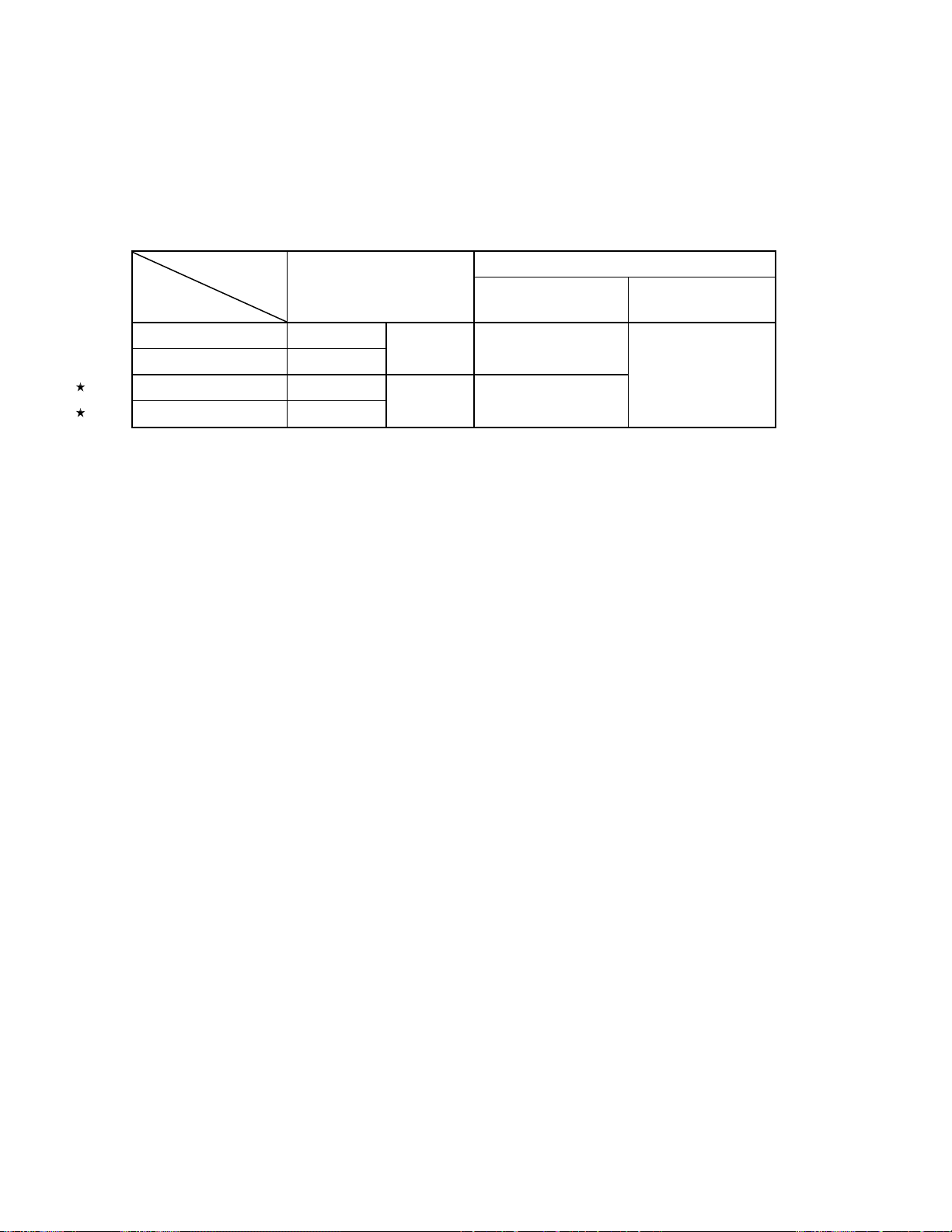
1.1 Features
• ROM and RAM capacities
CHAPTER 1 GENERAL
Item Data Memory
Part Number
µ
PD789488 Mask ROM
µ
PD78F9488 Flash memory
µ
PD789489 Mask ROM 1536 bytes
µ
PD78F9489 Flash memory
Program Memory
(ROM)
32 KB 1024 bytes 28 × 4 bits
48 KB
Internal RAM LCD Display RAM
• Minimum instruction execution time can be selected from high speed (0.4
system clock), low speed (1.6
µ
s: @5.0 MHz operation with main system clock), and ultra low speed (122 µs:
@32.768 kHz operation with subsystem clock)
• A circuit to multiply the subsystem clock by 4 is selectable (15.26
µ
s: @131 kHz operation: 32.768 kHz subsystem
clock × 4)
• I/O ports: 45 (N-ch open-drain: 4)
• Timer: 6 channels
• Serial interface: 2 channels
• 10-bit resolution A/D converter: 8 channels
• LCD controller/driver (on-chip voltage booster)
Segment signals: 28, common signals: 4
• On-chip multiplier: 8 bits × 8 bits = 16 bits
• On-chip infrared remote controller receiver (
µ
PD789489, 78F9489 only)
• On-chip key return signal detector
• Supply voltage: V
DD = 1.8 to 5.5 V
1.2 Applications
µ
s: @5.0 MHz operation with main
CD radio-cassette players, portable audio, compact cameras, healthcare equipment, etc.
26 User’s Manual U15331EJ4V1UD
Page 27

CHAPTER 1 GENERAL
1.3 Ordering Information
Part Number Package Internal ROM
µ
PD789488GC-×××-8BT 80-pin plastic QFP (14 × 14) Mask ROM
µ
PD789488GK-×××-9EU 80-pin plastic TQFP (fine pitch) (12 × 12) Mask ROM
µ
PD78F9488GC-8BT 80-pin plastic QFP (14 × 14) Flash memory
µ
PD78F9488GK-9EU 80-pin plastic TQFP (fine pitch) (12 × 12) Flash memory
µ
PD789489GC-×××-8BT 80-pin plastic QFP (14 × 14) Mask ROM
µ
PD789489GK-×××-9EU 80-pin plastic TQFP (fine pitch) (12 × 12) Mask ROM
µ
PD78F9489GC-8BT 80-pin plastic QFP (14 × 14) Flash memory
µ
PD78F9489GK-9EU 80-pin plastic TQFP (fine pitch) (12 × 12) Flash memory
µ
PD789488GC-×××-8BT-A 80-pin plastic QFP (14 × 14) Mask ROM
µ
PD789488GK-×××-9EU-A 80-pin plastic TQFP (fine pitch) (12 × 12) Mask ROM
µ
PD78F9488GC-8BT-A 80-pin plastic QFP (14 × 14) Flash memory
µ
PD78F9488GK-9EU-A 80-pin plastic TQFP (fine pitch) (12 × 12) Flash memory
µ
PD789489GC-×××-8BT-A 80-pin plastic QFP (14 × 14) Mask ROM
µ
PD789489GK-×××-9EU-A 80-pin plastic TQFP (fine pitch) (12 × 12) Mask ROM
µ
PD78F9489GC-8BT-A 80-pin plastic QFP (14 × 14) Flash memory
µ
PD78F9489GK-9EU-A 80-pin plastic TQFP (fine pitch) (12 × 12) Flash memory
Remarks 1. ××× indicates ROM code suffix.
2. Products that have the part numbers suffixed by "-A" are lead-free products.
User’s Manual U15331EJ4V1UD 27
Page 28
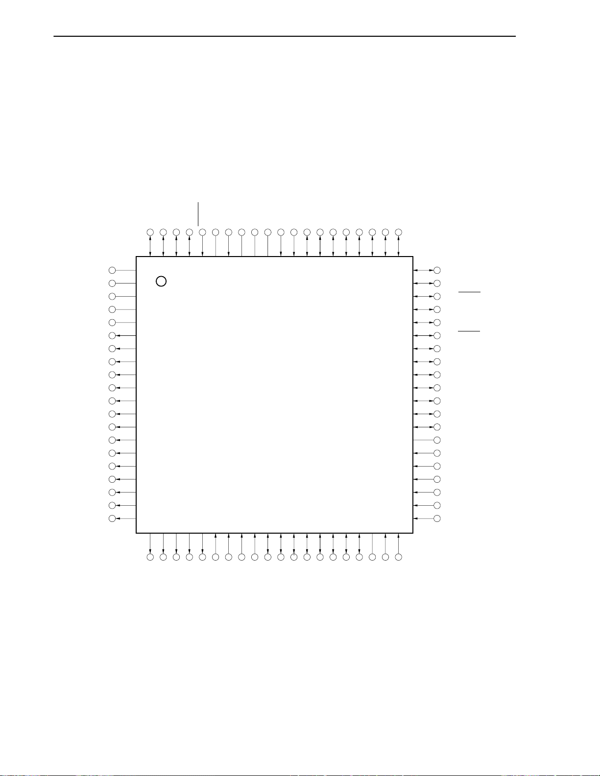
1.4 Pin Configuration (Top View)
(1) µPD789488, 78F9488
80-pin plastic QFP (14 × 14)
80-pin plastic TQFP (fine pitch) (12 × 12)
µ
PD789488GC-×××-8BT
µ
PD789488GC-×××-8BT-A
µ
PD789488GK-×××-9EU
µ
PD789488GK-×××-9EU-A
P50
P51
P52
P53
RESETX2X1
CHAPTER 1 GENERAL
µ
PD78F9488GC-8BT
µ
PD78F9488GC-8BT-A
µ
PD78F9488GK-9EU
µ
PD78F9488GK-9EU-A
)
PP
SSVDD
XT2
XT1
V
IC0 (V
P00/KR00
P01/KR01
P02/KR02
P03/KR03
P04/KR04
P05/KR05
P06/KR06
P07/KR07
CAPH
CAPL
V
LC2
V
LC1
V
LC0
COM0
COM1
COM2
COM3
S0
S1
S2
S3
S4
S5
S6
S7
S8
S9
S10
80 79 78 77 76 75 74 73 72 71 70 69 68 67 66 65 64 63 62 61
1
2
3
4
5
6
7
8
9
10
11
12
13
14
15
16
17
18
19
20
21 22 23 24 25 26 27 28 29 30 31 32 33 34 35 36 37 38 39 40
60
59
58
57
56
55
54
53
52
51
50
49
48
47
46
45
44
43
42
41
P10
P11
P20/SCK20/ASCK20
P21/SO20/TxD20
P22/SI20/RxD20
P23/SCK10
P24/SO10
P25/SI10
P30/INTP0/TO50/TMI60
P31/INTP1/TO60
P32/INTP2/TMI61/TO61
P33/INTP3/CPT20/TO20
P34/RIN
AV
SS
P60/ANI0/KR10
P61/ANI1/KR11
P62/ANI2/KR12
P63/ANI3/KR13
P64/ANI4/KR14
P65/ANI5/KR15
S11
S12
S13
S14
S15
Note 1
Note 1
P71/S17
P70/S16
Note 1
Note 1
P72/S18
P73/S19
Note 2
Note 2
P80/S20
P81/S21
Note 2
Note 2
P82/S22
P83/S23
Note 2
Note 2
P84/S24
P85/S25
Note 2
Note 2
P86/S26
P87/S27
DD
AV
P67/ANI7/KR17
P66/ANI6/KR16
Notes 1. Whether to use these pins as input port pins (P70 to P73) or segment outputs (S16 to S19) can be
selected in 1-bit units by means of a mask option or port function register (refer to 4.3 (3) Port function
registers and CHAPTER 20 MASK OPTIONS).
2. Whether to use these pins as I/O port pins (P80 to P87) or segment outputs (S20 to S27) can be
selected in 1-bit units by means of a mask option or port function register (refer to 4.3 (3) Port function
registers and CHAPTER 20 MASK OPTIONS).
28 User’s Manual U15331EJ4V1UD
Page 29
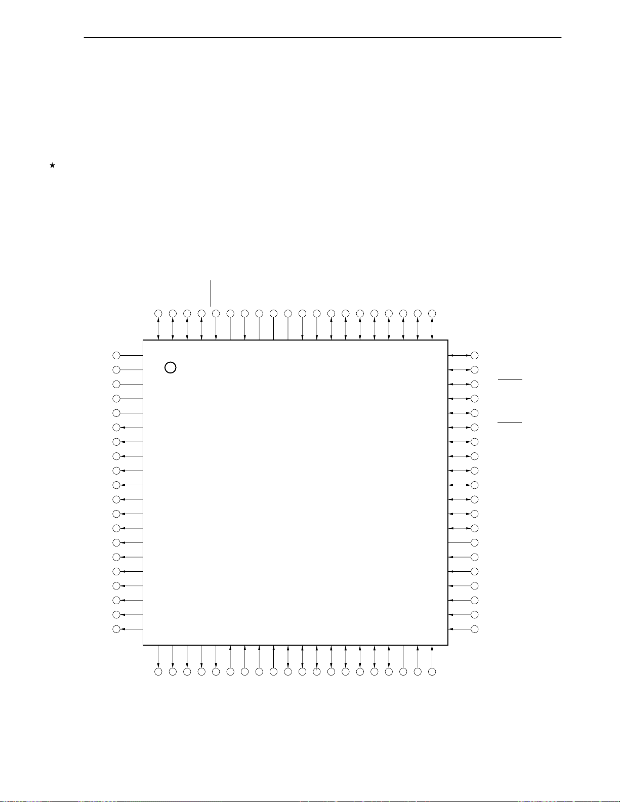
CHAPTER 1 GENERAL
Cautions 1. Connect the IC (Internally Connected) pin directly to V
2. Connect the AV
3. Connect the AV
DD pin to VDD.
SS pin to VSS.
Remark The parenthesized values apply to the
µ
PD78F9488
µ
PD789489, 78F9489
(2)
80-pin plastic QFP (14 × 14)
µ
PD789489GC-×××-8BT
µ
PD789489GC-×××-8BT-A
µ
PD78F9489GC-8BT
µ
PD78F9489GC-8BT-A
80-pin plastic TQFP (fine pitch) (12 × 12)
µ
PD789489GK-×××-9EU
µ
PD789489GK-×××-9EU-A
µ
PD78F9489GK-9EU
µ
PD78F9489GK-9EU-A
)
PP
SS.
CAPH
CAPL
V
LC2
V
LC1
V
LC0
COM0
COM1
COM2
COM3
S0
S1
S2
S3
S4
S5
S6
S7
S8
S9
S10
P50
P51
P52
P53
RESETX2X1
SSVDD
V
XT2
XT1
P00/KR00
IC0 (V
P01/KR01
P02/KR02
P03/KR03
P04/KR04
P05/KR05
80 79 78 77 76 75 74 73 72 71 70 69 68 67 66 65 64 63 62 61
1
2
3
4
5
6
7
8
9
10
11
12
13
14
15
16
17
18
19
20
21 22 23 24 25 26 27 28 29 30 31 32 33 34 35 36 37 38 39 40
P06/KR06
P07/KR07
60
59
58
57
56
55
54
53
52
51
50
49
48
47
46
45
44
43
42
41
P10
P11
P20/SCK20/ASCK20
P21/SO20/TxD20
P22/SI20/RxD20
P23/SCK10
P24/SO10
P25/SI10
P30/INTP0/TO50/TMI60
P31/INTP1/TO60
P32/INTP2/TMI61/TO61
P33/INTP3/CPT20/TO20
P34/RIN
AV
SS
P60/ANI0/KR10
P61/ANI1/KR11
P62/ANI2/KR12
P63/ANI3/KR13
P64/ANI4/KR14
P65/ANI5/KR15
S11
S12
S13
S14
S15
Note 1
Note 1
Note 1
Note 1
Note 2
Note 2
Note 2
Note 2
Note 2
Note 2
Note 2
P71/S17
P72/S18
P73/S19
P80/S20
P81/S21
P82/S22
P83/S23
P84/S24
P70/S16
User’s Manual U15331EJ4V1UD 29
P85/S25
Note 2
P86/S26
P87/S27
DD
AV
P67/ANI7/KR17
P66/ANI6/KR16
Page 30

CHAPTER 1 GENERAL
Notes 1. Whether to use these pins as input port pins (P70 to P73) or segment outputs (S16 to S19) can be
selected in 1-bit units by means of a mask option or port function register (refer to 4.3 (3) Port function
registers and CHAPTER 20 MASK OPTIONS).
2. Whether to use these pins as I/O port pins (P80 to P87) or segment outputs (S20 to S27) can be
selected in 1-bit units by means of a mask option or port function register (refer to 4.3 (3) Port function
registers and CHAPTER 20 MASK OPTIONS).
Cautions 1. Connect the IC (Internally Connected) pin directly to V
2. Connect the AV
3. Connect the AV
DD pin to VDD.
SS pin to VSS.
SS.
Remark The parenthesized values apply to the
µ
PD78F9489.
Pin Name
ANI0 to ANI7: Analog input
ASCK20: Asynchronous serial input
AV
DD: Analog power supply
SS: Analog ground
AV
CAPH, CAPL: LCD power supply capacitance
control
COM0 to COM3: Common output
CPT20: Capture trigger input
IC0: Internally connected
INTP0 to INTP3: External interrupt input
KR0 to KR7: Key return
KR00 to KR07: Key return
KR10 to KR17: Key return
P00 to P07: Port 0
P10, P11: Port 1
P20 to P25: Port 2
P30 to P34: Port 3
P60 to P67: Port 6
P70 to P73: Port 7
RESET: Reset
RIN: Remote control input
RxD0: Receive data
S0 to S27: Segment output
SCK10: Serial clock input/output
SI10: Serial data input
SO10: Serial data output
SCK20: Serial block input/output
SI20: Serial data input
SO20: Serial data output
TMI60, 61: Timer input
TO20,50,60,61: Timer output
TxD0: Transmit data
DD: Power supply
V
LC0 to VLC2: Power supply for LCD
V
PP: Programming power supply
V
SS: Ground
V
X1, X2: Crystal (Main system clock)
XT1, XT2: Crystal (Subsystem clock)
P80 to P87: Port 8
30 User’s Manual U15331EJ4V1UD
Page 31

CHAPTER 1 GENERAL
1.5 78K/0S Series Lineup
The products in the 78K/0S Series are listed below. The names enclosed in boxes are subseries names.
Products under development
µ
µ
µ
µ
78K/0S
Series
44-pin
42-/44-pin
30-pin
30-pin
20-pin
20-pin
44-pin
44-pin
30-pin
30-pin
30-pin
30-pin
144-pin
88-pin
80-pin
80-pin
80-pin
80-pin
64-pin
64-pin
64-pin
64-pin
64-pin
64-pin
52-pin
52-pin
44-pin
44-pin
44-pin
30-pin
30-pin
20-pin
20-pin
Products in mass production
Y Subseries products support SMB.
Small-scale package, general-purpose applications
PD789074 with added subsystem clock
PD789046
µ
µ
PD789026
µ
PD789088
µ
PD789074
PD789062
µ
µ
PD789052
Small-scale package, general-purpose applications and A/D converter
µ
PD789177
µ
µ
PD789167
µ
PD789134A
µ
PD789124A
µ
PD789114A
µ
PD789104A
LCD drive
µ
PD789835B
µ
PD789830
µ
PD789489
µ
PD789479
PD789417A
µ
PD789407A
µ
PD789456
µ
µ
PD789446
µ
PD789436
PD789426
µ
µ
PD789316
PD789306
µ
µ
PD789467
µ
PD789327
USB
µ
PD789800
Inverter control
µ
PD789842
On-chip bus controller
PD789852
µ
PD789850A
µ
Keyless entry
PD789862
µ
µ
PD789861
PD789860
µ
PD789177Y
PD789167Y
µ
µ
On-chip UART and capable of low voltage (1.8 V) operation
µ
PD789074 with enhanced timer and increased ROM, RAM capacity
PD789026 with enhanced timer
µ
RC oscillation version of the PD789052
PD789860 without EEPROM, POC, and LVI
µ
µ
PD789167 with enhanced A/D converter (10 bits)
µ
PD789104A with enhanced timer
µ
PD789124A with enhanced A/D converter (10 bits)
RC oscillation version of the PD789104A
µ
PD789104A with enhanced A/D converter (10 bits)
µ
PD789026 with added 8-bit A/D converter and multiplier
UART, 8-bit A/D, and dot LCD (Total display output pins: 96)
UART and dot LCD (40 × 16)
SIO, 10-bit A/D converter, and on-chip voltage booster type LCD (28 × 4)
SIO, 8-bit A/D converter, and resistance division type LCD (28 × 4)
PD789407A with enhanced A/D converter (10 bits)
µ
SIO, 8-bit A/D converter, and resistance division type LCD (28 × 4)
PD789446 with enhanced A/D converter (10 bits)
µ
SIO, 8-bit A/D, and on-chip voltage booster type LCD (15 × 4)
PD789426 with enhanced A/D converter (10 bits)
µ
SIO, 8-bit A/D, and on-chip voltage booster type LCD (5 × 4)
RC oscillation version of the PD789306
SIO and on-chip voltage booster type LCD (24 × 4)
8-bit A/D and on-chip voltage booster type LCD (23 × 4)
SIO and resistance division type LCD (24 × 4)
For PC keyboard and on-chip USB function
On-chip inverter controller and UART
µ
PD789850A with enhanced functions such as timer and A/D converter
On-chip CAN controller
PD789860 with enhanced timer, added SIO, and increased ROM, RAM capacity
µ
RC oscillation version of the PD789860
On-chip POC and key return circuit
Sensor
20-pin
20-pin
52-pin
64-pin
µ
PD789864
PD789863
µ
VFD drive
µ
PD789871
Meter control
PD789881
µ
On-chip analog macro for sensor
RC oscillation version of the PD789864
On-chip VFD controller (Total display output pins: 25)
UART and resistance division type LCD (26 × 4)
µ
Remark VFD (Vacuum Fluorescent Display) is referred to as FIPTM (Fluorescent Indicator Panel) in some
documents, but the functions of the two are the same.
User’s Manual U15331EJ4V1UD 31
Page 32

CHAPTER 1 GENERAL
The major functional differences between the subseries are listed below.
Series for General-purpose applications and LCD drive
8-Bit
A/D
Subseries Name
ROM
Capacity
Timer VDD Function
8-Bit 16-Bit Watch WDT
10-Bit
A/D
Serial
Interface
I/O
Remarks
MIN.
Value
µ
Small-scale
package,
general-
purpose
applications
Small-scale
package,
general-
purpose
applications
and A/D
converter
LCD drive
PD789046 16 KB 1 ch
µ
PD789026 4 KB to 16 KB
µ
PD789088 16 KB to
32 KB
µ
PD789074 2 KB to 8 KB 1 ch
µ
PD789062 RC oscillation
µ
PD789052
µ
PD789177
µ
PD789167
µ
PD789134A
µ
PD789124A 4 ch
µ
PD789114A
µ
PD789104A
µ
PD789835B 24 KB to
µ
PD789830 24 KB 1 ch
µ
PD789489 32 KB to
µ
PD789479 24 KB to
µ
PD789417A
µ
PD789407A
µ
PD789456
µ
PD789446 6 ch
µ
PD789436
µ
PD789426
µ
PD789316 RC oscillation
µ
PD789306
µ
PD789467 1 ch
µ
PD789327
4 KB 2 ch
16 KB to
24 KB
2 KB to 8 KB 1 ch
60 KB
48 KB
48 KB
12 KB to
24 KB
12 KB to
16 KB
8 KB to 16 KB
4 KB to 24 KB
Note Flash memory version: 3.0 V
1 ch 1 ch
1 ch 34
3 ch
−
3 ch 1 ch
1 ch
6 ch
−
1 ch
3 ch
2 ch
−
1 ch
−
1 ch
−
1 ch 1 ch
− −
(UART: 1 ch)
24
−
1 ch
8 ch
−
8 ch
−
−
4 ch
3 ch 37 1.8 V
−
8 ch
−
7 ch
−
−
6 ch
−
−
(UART: 1 ch)
−
4 ch
−
4 ch
−
1 ch
−
(UART: 1 ch)
2 ch
8 ch
(UART: 1 ch)
−
7 ch
1 ch
(UART: 1 ch)
−
6 ch
−
6 ch
−
2 ch
(UART: 1 ch)
1 ch 21
−
14
31
20
30 2.7 V
45
43
30
40
23
18
1.8 V
1.8 V
Note
1.8 V
−
version
−
−
RC oscillation
version
−
Dot LCD
supported
−
version
−
32 User’s Manual U15331EJ4V1UD
Page 33

Series for ASSP
CHAPTER 1 GENERAL
Subseries Name
USB
Inverter
control
µ
µ
µ
controller
µ
µ
entry
µ
µ
Sensor
µ
µ
ROM
Capacity
PD789800 8 KB 2 ch
PD789842 8 KB to 16 KB 3 ch
PD789852 24 KB to
32 KB
PD789850A 16 KB 1 ch
PD789861
PD789860
PD789862 16 KB 1 ch 2 ch
PD789864
PD789863
4 KB 2 ch
4 KB 1 ch
8-Bit 16-Bit Watch WDT
− −
Note 1
3 ch
1 ch
− −
Note 2
Timer VDD Function
1 ch
1 ch 1 ch 8 ch
1 ch
−
1 ch
−
1 ch
−
8-Bit
A/D
− −
−
4 ch
− −
−
10-Bit
A/D
2 ch
(USB: 1 ch)
1 ch
−
(UART: 1 ch)
8 ch 3 ch
(UART: 2 ch)
2 ch
−
(UART: 1 ch)
1 ch
(UART: 1 ch)
4 ch
Serial
Interface
−
I/O
MIN.
Value
31 4.0 V
30 4.0 V
31 On-chip bus
4.0 V
18
1.8 V
14 Keyless
22
5 1.9 V
Remarks
−
−
−
RC oscillation
version, on-
chip EEPROM
On-chip
EEPROM
On-chip
EEPROM
RC oscillation
version, on-
chip EEPROM
VFD drive µPD789871 4 KB to 8 KB 3 ch
Meter
control
µ
PD789881 16 KB 2 ch 1 ch
Notes 1. 10-bit timer: 1 channel
2. 12-bit timer: 1 channel
3. Flash memory version: 3.0 V
−
1 ch 1 ch
1 ch
−
− −
− −
1 ch 33 2.7 V
1 ch
(UART: 1 ch)
28 2.7 V
3
Note
−
−
User’s Manual U15331EJ4V1UD 33
Page 34

1.6 Block Diagram
CHAPTER 1 GENERAL
CPT20/TO20/P33
TO50/P30
TMI60/P30
TO60/P31
TMI61/TO61/P32
SCK20/ASCK20/P20
SO20/TxD20/P21
SI20/RxD20/P22
SCK10/P23
SO10/P24
SI10/P25
Note 4
RIN/P34
Note 3
KR0/P00 to
KR7/P07
Note 4
KR00/P00 to
Note 4
KR07/P07
KR10/ANI0/P60 to
KR17/ANI7/P67
ANI0/P60 to
ANI7/P67
S0 to S15
Note 1
S16 to S19
Note 2
S20 to S27
COM0 to COM3
V
LC0
to V
AV
AV
CAPH
CAPL
DD
SS
LC2
16-bit timer 20
8-bit timer
8-bit timer/
event counter 60
8-bit timer/
event counter 61
Watch timer
Watchdog timer
Serial
interface 20
Serial
interface 1A0
Remote control
signal receiver
A/D converter
LCD
controller/driver
50
Key return
Note 4
78K/0S
CPU core
RAM
VDDVSSIC0
ROM
(flash
memory)
RAM space
for LCD
data
(V
PP
)
Port 0
Port 1
Port 2
Port 3
Port 5
Port 6
Port 7
Port 8
Interrupt
control
Standby
control
System
control
Multiplier
P00 to P07
P10 to P11
P20 to P25
P30 to P34
P50 to P53
P60 to P67
P70 to P73
P80 to P87
INTP0/P30 to
INTP3/P33
RESET
X1
X2
XT1
XT2
Note 1
Note 2
Notes 1. Whether to use these pin as input ports (P70 to P73) or segment outputs (S16 to S19) can be selected
in 1-bit units by means of a mask option in the µPD789488, 789489 or a port mode register in the
µ
PD78F9488, 78F9489 (refer to 4.3 (3) Port function registers and CHAPTER 20 MASK OPTIONS).
2. Whether to use these pins as I/O port pins (P80 to P87) or segment outputs (S20 to S27) can be
selected in 1-bit units by means of a mask option in the
µ
PD78F9488, 78F9489 (refer to 4.3 (3) Port function registers and CHAPTER 20 MASK OPTIONS).
3. When
4. When
µ
PD789488, 78F9488 is used.
µ
PD789489, 78F9489 is used.
µ
PD789488 or a port mode register in the
Remark The parenthesized values apply to the flash memory version.
34 User’s Manual U15331EJ4V1UD
Page 35

CHAPTER 1 GENERAL
1.7 Overview of Functions
Item
Internal memory
Main system clock
(oscillation frequency)
Subsystem clock
(oscillation frequency)
Minimum instruction execution time
Subsystem clock multiplication function ×4 multiplication circuit (operating supply voltage: VDD = 2.7 to 5.5 V)
General-purpose registers 8 bits × 8 registers
Instruction set • 16-bit operations
Multiplier 8 bits × 8 bits = 16 bits
I/O ports Total: 45
Timers • 16-bit timer: 1 channel
Timer outputs 4
Serial interface UART/3-wire serial I/O mode: 1 channel
A/D converter 10-bit resolution × 8 channels
LCD controller/driver • Segment signal outputs: 28
Power supply method for LCD drive Internal voltage amplification method
Infrared remote control reception function Not provided Provided
Key return detection function 8 pins 16 pins
sources
Reset • Reset by RESET signal input
ROM 32 KB 32 KB (flash
High-speed RAM 1024 bytes
Low-speed RAM
LCD display RAM 28 bytes
Maskable Internal: 11, External: 5 Internal: 16, External: 6 Vectored interrupt
Non-maskable Internal: 1
µ
PD789488
Ceramic/crystal oscillation (1.0 to 5.0 MHz)
Crystal oscillation (32.768 kHz)
0.4 µs/1.6 µs (@5.0 MHz operation with main system clock)
122 µs (@32.768 kHz operation with subsystem clock)
15.26
µ
s (@131 kHz operation with ×4 subsystem clock)
• Bit manipulation (set, reset, test) etc.
CMOS I/O: 29
CMOS input: 12
N-ch open-drain I/O: 4
• 8-bit timer: 3 channels
• Watch timer: 1 channel
• Watchdog timer: 1 channel
3-wire serial I/O mode (with automatic transfer function): 1 channel
• Common signal outputs: 4
• Internal reset by watchdog timer
µ
memory)
−
Note 2
PD78F9488
Note 3
µ
PD789489
48 KB 48 KB (flash
512 bytes
µ
PD78F9489
memory)
Note 1
(1/2)
Notes 1. Whether a circuit to multiply the clock by 4 is used or not is selected by a mask option or the subclock
selection register.
2. 12 pins are used either as a port function or LCD segment output selected by a mask option or port
function register.
User’s Manual U15331EJ4V1UD 35
Page 36

CHAPTER 1 GENERAL
Item
Supply voltage VDD = 1.8 to 5.5 V
Operating ambient temperature TA = −40 to +85°C
Package • 80-pin plastic QFP (14 × 14)
µ
PD789488
• 80-pin plastic TQFP (fine pitch) (12 × 12)
µ
PD78F9488
An outline of the timer is shown below.
16-Bit
Timer 20
Operation
mode
Function
Interval timer
External event
counter
Timer outputs 1 output 1 output 1 output 1 output
Square-wave
outputs
Capture 1 input
Interrupt sources 1 1 1 1 2 2
−
− −
−
8-Bit
Timer 50
1 channel 1 channel 1 channel 1 channel
1 output 1 output 1 output
− − − − −
8-Bit
Timer 60
1 channel 1 channel
µ
PD789489
8-Bit
Timer 61
µ
PD78F9489
Watch
Timer
Note
1
− −
− −
− −
1 channel
(2/2)
Watchdog
Timer
Note
2
Notes 1. The watch timer can perform both watch timer and interval timer functions at the same time.
2. The watchdog timer has watchdog timer and interval timer functions. However, use the watchdog timer
by selecting either the watchdog timer function or interval timer function.
36 User’s Manual U15331EJ4V1UD
Page 37

CHAPTER 2 PIN FUNCTIONS
2.1 List of Pin Functions
(1) Port pins (1/2)
Pin Name I/O Function After Reset Alternate Function
Note 2
Note 1
Note 2
−
−
Note 1
Note 2
P00 to P07 I/O Port 0.
8-bit I/O port.
Input KR0 to KR7
KR00 to KR07
Input/output can be specified in 1-bit units.
When used as an input port, an on-chip pull-up resistor can be
specified in 1-bit units by pull-up resistor option register B0
(PUB0) or the key return mode register (KRM00).
P10, P11 I/O Port 1.
Input
2-bit I/O port.
Input/output can be specified in 1-bit units.
When used as an input port, an on-chip pull-up resistor can be
specified in 1-bit units by pull-up resistor option register B1
(PUB1).
P20 SCK20/ASCK20
P21 SO20/TxD20
P22 SI20/RxD20
P23 SCK10
P24 SO10
P25
P30 INTP0/TO50/TMI60
P31 INTP1/TO60
P32 INTP2/TMI61/TO61
P33 INTP3/CPT20/TO20
P34
P50 to P53 I/O Port 5.
I/O Port 2.
6-bit I/O port.
Input/output can be specified in 1-bit units.
When used as an input port, an on-chip pull-up resistor can be
specified in 1-bit units by pull-up resistor option register B2
(PUB2).
I/O Port 3.
5-bit I/O port.
Input/output can be specified in 1-bit units.
When used as an input port, on-chip pull-up resistors can be
specified in 1-bit units by pull-up resistor option register B3
(PUB3).
Input
SI10
Input
RIN
Input
4-bit N-ch open-drain I/O port.
Input/output can be specified in 1-bit units.
For mask ROM version, an on-chip pull-up resistor can be
specified by mask option.
P60 to P67 Input Port 6.
8-bit input port.
Input ANI0 to ANI7
ANI0/KR10 to
ANI7/KR17
Notes 1. µPD789488 and 78F9488 only
2. µPD789489 and 78F9489 only
User’s Manual U15331EJ4V1UD 37
Page 38

CHAPTER 2 PIN FUNCTIONS
(1) Port pins (2/2)
Pin Name I/O Function After Reset Alternate Function
P70 to P73
P80 to P87
Note 1
Input Port 7.
Note 2
I/O Port 8.
4-bit input port.
(Only when input port is selected by mask option or port
function register)
8-bit I/O port.
(Only when I/O port is selected by mask option or port function
register)
Input
Input
−
−
Notes 1. Whether to use these pins as input port pins (P70 to P73) or segment outputs (S16 to S19) can be
selected in 1-bit units by means of a mask option in the
µ
PD789488, 789489 or a port mode register in
the µPD78F9488, 78F9489 (refer to 4.3 (3) Port function registers and CHAPTER 20 MASK
OPTIONS).
2. Whether to use these pins as I/O port pins (P80 to P87) or segment outputs (S20 to S27) can be
selected in 1-bit units by means of a mask option in the
the
µ
PD78F9488, 78F9489 (refer to 4.3 (3) Port function registers and CHAPTER 20 MASK
µ
PD789488, 789489 or a port mode register in
OPTIONS).
(2) Non-port pins (1/2)
Pin Name I/O Function After Reset Alternate Function
INTP0 P30/TO50/TMI60
INTP1 P31/TO60
INTP2 P32/TMI61/TO61
INTP3
KR0 to KR7
KR00 to
Note 2
KR07
KR10 to
KR17
TO20 Output 16-bit timer 20 output Input P33/INTP3/CPT20
CPT20 Output Capture edge input of 16-bit timer 20 Input P33/INTP3/TO20
TO50 Output 8-bit timer 50 output Input P30/INTP0/TMI60
TO60 Output 8-bit timer 60 output Input P31/INTP1
TO61 Output 8-bit timer 61 output Input P32/INTP2/TMI61
TMI60 Input External count clock input to 8-bit timer 60 Input P30/INTP0/TO50
TMI61 Input External count clock input to 8-bit timer 61 Input P32/INTP2/TO61
SCK20 P20/ASCK20
SCK10
SO20 P21/TxD20
SO10
SI20 P22/RxD20
SI10
ASCK20 Input Serial clock input of asynchronous serial interface
TxD20 Output Serial data output of asynchronous serial interface Input P21/SO20
RxD20 Input Serial data input of asynchronous serial interface
RIN
Note 2
Note 2
Input Remote control reception data input Input P34
Input External interrupt input for which the valid edge (rising edge, falling
edge, or both rising and falling edges) can be specified.
Note 1
Input Key return signal detection Input P00 to P07
Input Key return signal detection Input
I/O Serial clock input/output of serial interface Input
Output Serial data output of serial interface Input
Input Serial data input of serial interface
Input
P33/CPT20/TO20
P00 to P07
P60/ANI0 to
P67/ANI7
P23
P24
Input
P25
Input P20/SCK20
Input P22/SI20
Notes 1. µPD789488 and 78F9488 only
2.
µ
PD789489 and 78F9489 only
38
User’s Manual U15331EJ4V1UD
Page 39

CHAPTER 2 PIN FUNCTIONS
(2) Non-port pins (2/2)
Pin Name I/O Function After Reset Alternate Function
S0 to S15 LCD controller/driver segment signal outputs Low-level
S16 to S19
S20 to S27
COM0 to COM3 Output LCD controller/driver common signal outputs Low-level
VLC0 to VLC2 – LCD drive voltage – –
CAPH, CAPL − LCD drive voltage booster capacitor connection pin – –
ANI0 to ANI7 – A/D converter analog input – P60 to P67
AVSS – A/D converter ground potential – –
AVDD – A/D converter analog power supply – –
X1 Input – –
X2 –
XT1 Input – –
XT2 –
RESET Input System reset input Input –
VDD – Positive power supply – –
VSS – Ground potential – –
IC0 – Internally connected. Connect directly to VSS. – –
VPP – Sets flash memory programming mode. Used to apply high
Output
Note 1
Only when segment output is selected by
Note 2
mask option
Only when segment output is selected by
mask option
Connecting crystal resonator for main system clock oscillation
Connecting crystal resonator for subsystem clock oscillation
voltage when a program is written or verified.
output
output
P60/KR10 to
P67/KR17
– –
– –
– –
–
–
–
–
Note 3
Note 4
Notes 1. Whether to use these pins as input ports pins (P70 to P73) or segment outputs (S16 to S19) can be
selected in 1-bit units by means of a mask option in the µPD789488, 789489 or a port mode register in
µ
PD78F9488, 78F9489 (refer to 4.3(3) Port function registers and CHAPTER 20 MASK
the
OPTIONS).
2. Whether to use these pins as I/O port pins (P80 to P87) or segment outputs (S20 to S27) can be
selected in 1-bit units by means of a mask option in the
µ
PD78F9488, 78F9489 (refer to 4.3(3) Port function registers and CHAPTER 20 MASK
the
µ
PD789488, 789489 or a port mode register in
OPTIONS).
3.
4.
µ
PD789488 and 78F9488 only
µ
PD789489 and 78F9489 only
User’s Manual U15331EJ4V1UD
39
Page 40

CHAPTER 2 PIN FUNCTIONS
2.2 Description of Pin Functions
2.2.1 P00 to P07 (Port 0)
These pins constitute an 8-bit I/O port. In addition, these pins enable key return signal detection.
Port 0 can be specified in the following operation modes in 1-bit units.
(1) Port mode
These pins constitute an 8-bit I/O port and can be set in the input or output port mode in 1-bit units by port
mode register 0 (PM0). When used as an input port, use of an on-chip pull-up resistor can be specified by
pull-up resistor option register B0 (PUB0) in 1-bit units.
(2) Control mode
In this mode, P00 to P07 function as key return signal detection pins (KR0 to KR7 (
KR00 to KR07 (
2.2.2 P10, P11 (Port 1)
These pins constitute a 2-bit I/O port and can be set in the input or output port mode in 1-bit units by port mode
register 1 (PM1). When used as an input port, use of an on-chip pull-up resistor can be specified by pull-up resistor
option register B1 (PUB1) in 1-bit units.
2.2.3 P20 to P25 (Port 2)
µ
PD789489, 78F9489)).
µ
PD789488, 78F9488),
These pins constitute a 6-bit I/O port. In addition, these pins enable serial interface data I/O and serial clock I/O.
Port 2 can be specified in the following operation modes in 1-bit units.
(1) Port mode
In this mode, P20 to P25 function as a 6-bit I/O port. Port 2 can be set in the input or output port mode in 1-
bit units by port mode register 2 (PM2). When used as an input port, use of an on-chip pull-up resistor can
be specified by pull-up resistor option register B2 (PUB2) in 1-bit units.
(2) Control mode
In this mode, P20 to P25 function as the serial interface data I/O and serial clock I/O.
(a) SI20, SO20, SI10, SO10
These are the serial data I/O pins of the serial interface.
(b) SCK20, SCK10
These are the serial clock I/O pins of the serial interface.
(c) RxD20, TxD20
These are the serial data I/O pins of the asynchronous serial interface.
(d) ASCK20
This is the serial clock input pin of the asynchronous serial interface.
Caution When using P20 to P25 as serial interface pins, the I/O mode and output latch must be set
according to the functions to be used. For the details of the setting, refer to Table 11-2 Serial
Interface 20 Operation Mode Setting and 12.3 (1) Serial operation mode register 1A0 (CSIM1A0).
40
User’s Manual U15331EJ4V1UD
Page 41

2.2.4 P30 to P34 (Port 3)
CHAPTER 2 PIN FUNCTIONS
These pins constitute a 5-bit I/O port. In addition, they also function as timer I/O, external interrupt input, and
Note
remote control receive data input
.
Port 3 can be specified in the following operation modes in 1-bit units.
(1) Port mode
In this mode, P30 to P34 function as a 5-bit I/O port. Port 3 can be set in the input or output port mode in 1-
bit units by port mode register 3 (PM3). When used as an input port, use of an on-chip pull-up resistor can
be specified by pull-up resistor option register B3 (PUB3) in 1-bit units.
(2) Control mode
In this mode, P30 to P34 function as timer I/O, external interrupt input, and remote control receive data
Note
input
.
(a) TMI60, TMI61
These are the external clock input pins of timers 60 and 61.
(b) TO20, TO50, TO60, TO61
These are the timer output pins of timers 20, 50, 60, and 61.
(c) CPT20
This is the capture edge input pin of 16-bit timer 20.
(d) INTP0 to INTP3
These are external interrupt input pins for which valid edges (rising edge, falling edge, or both rising and
falling edges) can be specified.
(e) RIN
Note
This is the data input pin of the remote controller receiver.
µ
Note
PD789489 and 78F9489 only
2.2.5 P50 to P53 (Port 5)
These pins constitute as a 4-bit N-ch open-drain I/O port. Port 5 can be set in the input or output port mode in 1-
bit units by port mode register 5 (PM5). In the mask ROM version, use of an on-chip pull-up resistor can be specified
by a mask option in 1-bit units.
User’s Manual U15331EJ4V1UD
41
Page 42

2.2.6 P60 to P67 (Port 6)
CHAPTER 2 PIN FUNCTIONS
This is an 8-bit input-only port. In addition to a general-purpose input port function, it has A/D converter input and
Note
key return signal detection
functions.
(1) Port mode
In this mode, P60 to P67 function as an 8-bit input-only port.
(2) Control mode
In this mode, P60 to P67 function as the analog inputs of the A/D converter and key return signal detection
Note
.
pins
(a) ANI0 to ANI7
These are the analog input pins of the A/D converter.
Note
(b) KR10 to KR17
These are the key return signal detection pins.
Note µPD789489 and 78F9489 only
2.2.7 P70 to P73 (Port 7)
These pins constitute a 4-bit input-only port. This port can be used only when the port function is selected by a
µ
mask option in the
PD789488, 789489 or by a port function register in the µPD78F9488, 78F9489.
2.2.8 P80 to P87 (Port 8)
These pins constitute an 8-bit I/O port. Port 8 can be set in the input or output mode in 1-bit units by port mode
register 8 (PM8). This port can be used only when the port function is selected by a mask option in the µPD789488,
789489 or by a port function register in the
µ
PD78F9488, 78F9489.
2.2.9 S0 to S27
Note
These pins are the segment signal output pins for the LCD controller/driver.
Note Pins S16 through S27 can be used only when segment output is selected by a mask option in the
µ
PD789488, 789489 or by a port function register in the µPD78F9488, 78F9489.
2.2.10 COM0 to COM3
These pins are the common signal output pins for the LCD controller/driver.
2.2.11 V
LC0 to VLC2
These pins are the power supply voltage pins for driving the LCD.
2.2.12 CAPH, CAPL
These pins are the capacitor connection pins for driving the LCD.
42
User’s Manual U15331EJ4V1UD
Page 43

CHAPTER 2 PIN FUNCTIONS
2.2.13 RESET
This pin inputs an active-low system reset signal.
2.2.14 X1, X2
These pins are used to connect a crystal resonator for main system clock oscillation.
To supply an external clock, input the clock to X1 and input the inverted signal to X2.
2.2.15 XT1, XT2
These pins are used to connect a crystal resonator for subsystem clock oscillation.
To supply an external clock, input the clock to XT1 and input the inverted signal to XT2.
2.2.16 AV
DD
This is the analog power supply pin of the A/D converter. Always use the same potential as that of the VDD pin even
when the A/D converter is not used.
2.2.17 AV
SS
This is the ground potential pin of the A/D converter. Always use the same potential as that of the VSS pin even
when the A/D converter is not used.
2.2.18 V
DD
This is the positive power supply pin.
2.2.19 V
SS
This is the ground pin.
2.2.20 V
PP (flash memory version only)
A high voltage should be applied to this pin when the flash memory programming mode is set and when the
program is written or verified.
Handle the pins in either of the following ways.
• Independently connect a 10 kΩ pull-down resistor.
• Switch this pin to be directly connected to the dedicated flash programmer in programming mode or to V
normal operation mode using a jumper on the board.
If the wiring between the V
PP pin and VSS pin is very long or external noise is superimposed on the VPP pin, the
user program may not run correctly.
SS in
User’s Manual U15331EJ4V1UD
43
Page 44

CHAPTER 2 PIN FUNCTIONS
2.2.21 IC0 (mask ROM version only)
µ
The IC0 (Internally Connected) pin is used to set the
the normal operation mode, directly connect this pin to the V
If there is a potential difference between the IC0 pin and V
PD789489 Subseries in the test mode before shipment. In
SS pin with as short a wiring length as possible.
SS pin due to a long wiring length or external noise
superimposed on the IC0 pin, the user program may not run correctly.
• Directly connect the IC0 pin to the V
IC0
V
SS
Keep short
SS pin.
44
User’s Manual U15331EJ4V1UD
Page 45

CHAPTER 2 PIN FUNCTIONS
2.3 Pin I/O Circuits and Recommended Connection of Unused Pins
The I/O circuit type of each pin and recommended connection of unused pins are shown in Table 2-1.
For the I/O circuit configuration of each type, see Figure 2-1.
Table 2-1. Types of Pin I/O Circuits (1/2)
Pin Name I/O Circuit Type I/O Recommended Connection of Unused Pins
P00/KR0 to P07/KR7
P00/KR00 to P07/KR07
P10, P11 5-A
P20/SCK20/ASCK20 8-A
P21/SO20/TxD20 5-A
P22/SI20/RxD20
P23/SCK10
P24/SO10 5-A
P25/SI10
P30/INTP0/TO50/
TMI60
P31/INTP1/TO60
P32/INTP2/TO61/
TMI61
P33/INTP3/CPT20/
TO20
Note 1
P34
Note 2
P34/RIN
P50 to P53
(mask ROM version)
P50 to P53
(flash memory version)
P60/ANI0 to P67/ANI7
P60/ANI0/KR10 to
P67/ANI7/KR17
P70 to P73
P80 to P87
Note 3
Note 3
COM0 to COM3 18
S0 to S15
S16 to S19
S20 to S27
Note 4
Note 4
CAPH, CAPL
VLC0 to VLC2
AVDD Connect directly to VDD
AVSS
Notes 1. When µPD789488, 78F9488 is used.
2. When
3. Only when port pin is selected by mask option or port function register.
4. Only when segment output pin is selected by mask option or port function register.
Note 1
Note 2
I/O
8-A
Input: Independently connect to V
Output: Leave open.
DD or VSS via a resistor.
8-A
8-A
Input: Independently connect to V
SS via a resistor.
Output: Leave open.
13-W
Input: Independently connect to V
DD via a resistor.
Output: Leave open.
13-V
Note 2
Note 1
9-C
Input Connect to V
DD or VSS.
2-H
5-K I/O Input: Independently connect to VDD or VSS via a resistor.
Output: Leave open.
Output
Leave open.
17
– –
Connect directly to VSS
µ
PD789489, 78F9489 is used.
User’s Manual U15331EJ4V1UD
45
Page 46

CHAPTER 2 PIN FUNCTIONS
Table 2-1. Types of Pin I/O Circuits (2/2)
Pin Name I/O Circuit Type I/O Recommended Connection of Unused Pins
XT1 Input Connect to VSS.
XT2
–
– Leave open.
RESET 2 Input –
IC0 Connect directly to VSS.
VPP
– –
Independently connect a 10 kΩ pull-down resistor, or connect
directly to V
SS.
Figure 2-1. I/O Circuit Types (1/2)
Type 2 Type 2-H
IN
IN
Input
enable
Schmitt-triggered input with hysteresis characteristics.
Type 5-A Type 5-K
V
DD
Pull-up
enable
Data
Output
disable
V
V
SS
DD
P-ch
N-ch
P-ch
IN/OUT
Data
Output
disable
Input
enable
Input
enable
Type 8-A Type 9-C
V
DD
Pull-up
enable
Data
V
DD
P-ch
P-ch
IN
IN/OUT
Output
disable
N-ch
V
SS
P-ch
N-ch
V
DD
P-ch
IN/OUT
N
-ch
Comparator
+
SS
AV
V
REF
(Threshold voltage)
Input
enable
46
User’s Manual U15331EJ4V1UD
Page 47

CHAPTER 2 PIN FUNCTIONS
Figure 2-1. I/O Circuit Types (2/2)
Type 13-W Type 13-V
V
DD
Data
Output
disable
Input
enable
Middle-voltage input buffer
Mask
option
IN/OUT
N
-ch
V
SS
Data
Output
disable
Input
enable
Type 17 Type 18
V
LC0
V
LC1
SEG
data
LC2
V
P-ch
P-ch
N-ch
P-ch
OUT
N-ch
P-ch
N-ch
N-ch
VLC0
VLC1
COM
data
VLC2
Middle-voltage input buffer
P-ch
P-ch
N-ch
P-ch
N-ch
N-ch
P-ch
N-ch
IN/OUT
N
-ch
V
SS
N-ch
OUT
P-ch
User’s Manual U15331EJ4V1UD
47
Page 48

CHAPTER 3 CPU ARCHITECTURE
3.1 Memory Space
The µPD789489 Subseries can access 64 KB of memory space. Figures 3-1 to 3-4 show the memory maps.
Data memory
space
F F F F H
F F 0 0 H
F E F F H
F B 0 0 H
F A F F H
F A 1 C H
F A 1 B H
F A 0 0 H
F 9 F F H
8 0 0 0 H
7 F F F H
Figure 3-1. Memory Map (
Special function registers
256 × 8 bits
Internal high-speed RAM
1024 × 8 bits
Reserved
LCD display RAM
28 × 4 bits
Reserved
µ
PD789488)
7 F F F H
Program memory
space
0 0 0 0 H
Internal ROM
32768 × 8 bits
0 0 8 0 H
0 0 7 F H
0 0 4 0 H
0 0 3 F H
0 0 2 E H
0 0 2 D H
0 0 0 0 H
Program area
CALLT table area
Program area
Vector table area
48 User’s Manual U15331EJ4V1UD
Page 49

Data memory
space
F F F F H
F F 0 0 H
F E F F H
F B 0 0 H
F A F F H
F A 1 C H
F A 1 B H
F A 0 0 H
F 9 F F H
8 0 0 0 H
7 F F F H
CHAPTER 3 CPU ARCHITECTURE
Figure 3-2. Memory Map (µPD78F9488)
Special function registers
256 × 8 bits
Internal high-speed RAM
1024 × 8 bits
Reserved
LCD display RAM
28 × 4 bits
7 F F F H
Reserved
Program memory
space
0 0 0 0 H
Flash memory
32768 × 8 bits
Program area
0 0 8 0 H
0 0 7 F H
0 0 4 0 H
0 0 3 F H
0 0 2 E H
0 0 2 D H
0 0 0 0 H
CALLT table area
Program area
Vector table area
User’s Manual U15331EJ4V1UD 49
Page 50

Data memory
space
Program memory
space
F F F F H
F F 0 0 H
F E F F H
F B 0 0 H
F A F F H
F A 1 C H
F A 1 B H
F A 0 0 H
F 9 F F H
F 7 0 0 H
F 6 F F H
F 5 0 0 H
F 4 F F H
C 0 0 0 H
B F F F H
0 0 0 0 H
CHAPTER 3 CPU ARCHITECTURE
Figure 3-3. Memory Map (µPD789489)
Special function registers
256 × 8 bits
Internal high-speed RAM
1024 × 8 bits
Reserved
LCD display RAM
28 × 4 bits
Reserved
Internal low-speed
512 × 8 bits
Reserved
Internal ROM
49152 × 8 bits
B F F F H
0 0 8 0 H
0 0 7 F H
0 0 4 0 H
0 0 3 F H
0 0 3 0 H
0 0 2 F H
0 0 0 0 H
Program area
CALLT table area
Program area
Vector table area
50 User’s Manual U15331EJ4V1UD
Page 51

Data memory
space
Program memory
space
F F F F H
F F 0 0 H
F E F F H
F B 0 0 H
F A F F H
F A 1 C H
F A 1 B H
F A 0 0 H
F 9 F F H
F 7 0 0 H
F 6 F F H
F 5 0 0 H
F 4 F F H
C 0 0 0 H
B F F F H
0 0 0 0 H
CHAPTER 3 CPU ARCHITECTURE
Figure 3-4. Memory Map (µPD78F9489)
Special function registers
256 × 8 bits
Internal high-speed RAM
1024 × 8 bits
Reserved
LCD display RAM
28 × 4 bits
Reserved
Internal low-speed RAM
512 × 8 bits
Reserved
Flash memory
49152 × 8 bits
B F F F H
0 0 8 0 H
0 0 7 F H
0 0 4 0 H
0 0 3 F H
0 0 3 0 H
0 0 2 F H
0 0 0 0 H
Program area
CALLT table area
Program area
Vector table area
User’s Manual U15331EJ4V1UD 51
Page 52

CHAPTER 3 CPU ARCHITECTURE
3.1.1 Internal program memory space
The internal program memory space stores programs and table data. This space is usually addressed by the
program counter (PC).
The
µ
PD789489 Subseries provide internal ROM (or flash memory) with the following capacity for each product.
Table 3-1. Internal ROM Capacity
Part Number Internal ROM
Structure Capacity
µ
PD789488 Mask ROM
µ
PD78F9488 Flash memory
µ
PD789489 Mask ROM
µ
PD78F9489 Flash memory
32768 × 8 bits
49152 × 8 bits
The following areas are allocated to the internal program memory space.
(1) Vector table area
The 46-byte area of addresses 0000H to 002DH is reserved in the
µ
PD789488 and 78F9488, and the 48-
byte area of address 0000H to 002FH is reserved in the µPD789489 and 78F9489 as a vector table area.
This area stores program start addresses to be used when branching by RESET input or interrupt request
generation. Of a 16-bit program address, the lower 8 bits are stored in an even address, and the higher 8
bits are stored in an odd address.
Table 3-2. Vector Table
Vector Table Address Interrupt Request Vector Table Address Interrupt Request
0000H RESET input 0018H INTTM20
0004H INTWDT 001AH INTTM50
0006H INTP0 001CH INTTM60
0008H INTP1 001EH INTTM61
000AH INTP2 0020H INTAD0
000CH INTP3 0022H INTWT
000EH INTRIN
0010H INTSR20/INTCSI20 0026H INTRERR
0012H INTCSI10 0028H INTGP
0014H INTST20 002AH INTREND
0016H INTWTI 002CH INTDFULL
002EH INTKR01
Note
0024H INTKR00
Note
Note
Note
Note
Note
µ
Note
PD789489 and 78F9489 only. There are no interrupt requests corresponding to vector table
µ
addresses 000EH, and 0026H through 002EH for
PD789488 and 78F9488.
(2) CALLT instruction table area
The subroutine entry address of a 1-byte call instruction (CALLT) can be stored in the 64-byte area of
addresses 0040H to 007FH.
52 User’s Manual U15331EJ4V1UD
Page 53

CHAPTER 3 CPU ARCHITECTURE
3.1.2 Internal data memory space
(1) Internal high-speed RAM and internal low-speed RAM
The
µ
PD789489 Subseries products incorporate the internal high-speed RAM and internal low-speed RAM of
the following capacity for each product.
The internal high-speed RAM can also be used as a stack.
The internal low-speed RAM cannot be used as a stack.
Table 3-3. Internal High-Speed RAM, Internal Low-Speed RAM Capacity
Part Number Internal High-Speed RAM Internal Low-Speed RAM
µ
PD789488
µ
PD78F9488
µ
PD789489
µ
PD78F9489
1024 × 8 bits
(2) LCD display RAM
LCD display RAM is incorporated in the area between FA00H and FA1BH.
The LCD display RAM can also be used as ordinary RAM.
3.1.3 Special function register (SFR) area
−
512 × 8 bits
Special function registers (SFRs) of on-chip peripheral hardware are allocated in the area between FF00H and
FFFFH (see Table 3-4).
User’s Manual U15331EJ4V1UD 53
Page 54

CHAPTER 3 CPU ARCHITECTURE
3.1.4 Data memory addressing
µ
PD789489 Subseries is provided with a variety of addressing modes to make memory manipulation as
The
efficient as possible. At the addresses corresponding to data memory area (FB00H to FFFFH) especially, specific
addressing modes that correspond to the particular function of an area, such as the special function registers, are
available. Figures 3-5 to 3-8 show the data memory addressing modes.
F F F F H
F F 2 0 H
F F 1 F H
F F 0 0 H
F E F F H
Figure 3-5. Data Memory Addressing (
Special function registers
256 × 8 bits
SFR addressing
µ
PD789488)
F E 2 0 H
F E 1 F H
F B 0 0 H
F A F F H
F A 1 C H
F A 1 B H
F A 0 0 H
F 9 F F H
8 0 0 0 H
7 F F F H
Internal high-speed RAM
1024 × 8 bits
Reserved
LCD display RAM
28 × 4 bits
Reserved
Internal ROM
32768 × 8 bits
Short direct addressing
Direct addressing
Register indirect addressing
Based addressing
0 0 0 0 H
54 User’s Manual U15331EJ4V1UD
Page 55

F F F F H
F F 2 0 H
F F 1 F H
F F 0 0 H
F E F F H
Figure 3-6. Data Memory Addressing (µPD78F9488)
Special function registers
256 × 8 bits
CHAPTER 3 CPU ARCHITECTURE
SFR addressing
F E 2 0 H
F E 1 F H
F B 0 0 H
F A F F H
F A 1 C H
F A 1 B H
F A 0 0 H
F 9 F F H
8 0 0 0 H
7 F F F H
Internal high-speed RAM
1024 × 8 bits
Reserved
LCD display RAM
28 × 4 bits
Reserved
Flash memory
32768 × 8 bits
Short direct addressing
Direct addressing
Register indirect addressing
Based addressing
0 0 0 0 H
User’s Manual U15331EJ4V1UD 55
Page 56

F F F F H
CHAPTER 3 CPU ARCHITECTURE
Figure 3-7. Data Memory Addressing (µPD789489)
F F 2 0 H
F F 1 F H
F F 0 0 H
F E F F H
F E 2 0 H
F E 1 F H
F B 0 0 H
F A F F H
F A 1 C H
F A 1 B H
F A 0 0 H
F 9 F F H
F 7 0 0 H
F 6 F F H
F 5 0 0 H
F 4 F F H
C 0 0 0 H
B F F F H
Special function registers (SFR)
256 × 8 bits
Internal high-speed RAM
1024 × 8 bits
Reserved
LCD display RAM
28 × 4 bits
Reserved
Internal low-speed RAM
512 × 8 bits
Reserved
SFR addressing
Short direct addressing
Direct addressing
Register indirect addressing
Based addressing
0 0 0 0 H
Internal ROM
49152 × 8 bits
56 User’s Manual U15331EJ4V1UD
Page 57

F F F F H
F F 2 0 H
F F 1 F H
F F 0 0 H
F E F F H
F E 2 0 H
F E 1 F H
F B 0 0 H
F A F F H
F A 1 C H
F A 1 B H
F A 0 0 H
F 9 F F H
F 7 0 0 H
F 6 F F H
F 5 0 0 H
F 4 F F H
C 0 0 0 H
B F F F H
Figure 3-8. Data Memory Addressing (µPD78F9489)
Special function registers
256 × 8 bits
Internal high-speed RAM
1024 × 8 bits
Reserved
LCD display RAM
28 × 4 bits
Reserved
Internal low-speed
512 × 8 bits
Reserved
CHAPTER 3 CPU ARCHITECTURE
SFR addressing
Short direct addressing
Direct addressing
Register indirect addressing
Based addressing
0 0 0 0 H
Flash memory
49152 × 8 bits
User’s Manual U15331EJ4V1UD 57
Page 58

CHAPTER 3 CPU ARCHITECTURE
3.2 Processor Registers
The µPD789489 Subseries is provided with the following on-chip processor registers.
3.2.1 Control registers
The control registers contain special functions to control the program sequence status and stack memory. The
program counter, program status word, and stack pointer are control registers.
(1) Program counter (PC)
The program counter is a 16-bit register that holds the address information of the next program to be
executed.
In normal operation, the PC is automatically incremented according to the number of bytes of the instruction
to be fetched. When a branch instruction is executed, immediate data or register contents are set.
RESET input sets the reset vector table values at addresses 0000H and 0001H to the program counter.
Figure 3-9. Program Counter Configuration
015
PC14PC15PC PC13 PC12 PC11 PC10 PC9 PC8 PC7 PC6 PC5 PC4 PC3 PC2 PC1 PC0
(2) Program status word (PSW)
The program status word is an 8-bit register consisting of various flags to be set/reset by instruction
execution.
The program status word contents are automatically stacked upon interrupt request generation or PUSH
PSW instruction execution and are automatically restored upon execution of the RETI and POP PSW
instructions.
RESET input sets PSW to 02H.
Figure 3-10. Program Status Word Configuration
70
PSW
IE
Z 0 AC 0 0 1 CY
58 User’s Manual U15331EJ4V1UD
Page 59

(a) Interrupt enable flag (IE)
This flag controls interrupt request acknowledgement operations of the CPU.
When 0, IE is set to the interrupt disabled status (DI), and interrupt requests other than non-maskable
interrupts are all disabled.
When 1, IE is set to the interrupt enabled status (EI). Interrupt request acknowledgement enable is
controlled by the interrupt mask flag for the corresponding interrupt source.
IE is reset (0) upon DI instruction execution or interrupt acknowledgment and is set (1) upon EI
instruction execution.
(b) Zero flag (Z)
When the operation result is zero, this flag is set (1). It is reset (0) in all other cases.
(c) Auxiliary carry flag (AC)
If the operation result has a carry from bit 3 or a borrow at bit 3, this flag is set (1). It is reset (0) in all
other cases.
(d) Carry flag (CY)
This flag stores an overflow or underflow upon add/subtract instruction execution. It stores the shift-out
value upon rotate instruction execution and functions as a bit accumulator during bit manipulation
instruction execution.
CHAPTER 3 CPU ARCHITECTURE
User’s Manual U15331EJ4V1UD 59
Page 60

CHAPTER 3 CPU ARCHITECTURE
(3) Stack pointer (SP)
This is a 16-bit register that holds the start address of the memory stack area. Only the internal high-speed
RAM area can be set as the stack area.
Figure 3-11. Stack Pointer Configuration
SP14SP15SP SP13 SP12 SP11 SP10 SP9 SP8 SP7 SP6 SP5 SP4 SP3 SP2 SP1 SP0
The SP is decremented ahead of write (save) to the stack memory and is incremented after read (restore)
from the stack memory.
Each stack operation saves/restores data as shown in Figures 3-12 and 3-13.
Caution Since RESET input makes the SP contents undefined, be sure to initialize the SP before
instruction execution.
Figure 3-12. Data to Be Saved to Stack Memory
015
SP SP _ 2
SP _ 2
SP _ 1
SP
SP
SP + 1
PUSH rp
instruction
Lower
register pairs
Higher
register pairs
SP SP _ 2
SP _ 2
SP _ 1
SP
CALL, CALLT
instructions
PC7 to PC0
PC15 to PC8
Figure 3-13. Data to Be Restored from Stack Memory
instruction
Lower
register pairs
Higher
register pairs
SP
SP + 1
RET instructionPOP rp
PC7 to PC0
PC15 to PC8
SP SP _ 3
SP _ 3
SP _ 2
SP _ 1
SP
SP
SP + 1
Interrupt
PC7 to PC0
PC15 to PC8
PSW
RETI instruction
PC7 to PC0
PC15 to PC8
SP SP + 2
SP SP + 2
60 User’s Manual U15331EJ4V1UD
SP + 2
SP SP + 3
PSW
Page 61

CHAPTER 3 CPU ARCHITECTURE
3.2.2 General-purpose registers
The general-purpose registers consist of eight 8-bit registers (X, A, C, B, E, D, L, and H).
Each register can be used as an 8-bit register, or two 8-bit registers in pairs can be used as a 16-bit register (AX,
BC, DE, and HL).
General-purpose registers can be described in terms of function names (X, A, C, B, E, D, L, H, AX, BC, DE, or HL)
or absolute names (R0 to R7 and RP0 to RP3).
Figure 3-14. General-Purpose Register Configuration
(a) Absolute names
16-bit processing 8-bit processing
R7
RP3
R6
R5
RP2
R4
R3
RP1
R2
R1
RP0
R0
15 0 7 0
(b) Function names
16-bit processing 8-bit processing
H
HL
L
D
DE
BC
E
B
C
A
AX
X
15 0 7 0
User’s Manual U15331EJ4V1UD 61
Page 62

CHAPTER 3 CPU ARCHITECTURE
3.2.3 Special function registers (SFRs)
Unlike a general-purpose register, each special function register has a special function.
The special function registers are allocated in the 256-byte area of FF00H to FFFFH.
Special function registers can be manipulated, like general-purpose registers, by operation, transfer, and bit
manipulation instructions. The manipulatable bit units (1, 8, and 16) differ depending on the special function register
type.
The manipulatable bits can be specified as follows.
• 1-bit manipulation
Describe the symbol reserved by the assembler for the 1-bit manipulation instruction operand (sfr.bit). This
manipulation can also be specified with an address.
• 8-bit manipulation
Describe the symbol reserved by the assembler for the 8-bit manipulation instruction operand (sfr). This
manipulation can also be specified with an address.
• 16-bit manipulation
Describe the symbol reserved by the assembler for the 16-bit manipulation instruction operand. When
addressing an address, describe an even address.
Table 3-4 lists the special function registers. The meanings of the symbols in this table are as follows.
• Symbol
Indicates the addresses of the implemented special-function registers. The symbols shown in this column are
reserved words in the assembler, and have already been defined as sfr variables by the #pragma sfr directive in
the C compiler. Therefore, these symbols can be used as instruction operands if an assembler or integrated
debugger is used.
• R/W
Indicates whether the special function register in question can be read or written.
R/W: Read/write
R: Read only
W: Write only
• Bit unit for manipulation
Indicates the bit units (1, 8, 16) in which the special function register in question can be manipulated.
• After reset
Indicates the status of the special function register when the RESET signal is input.
62 User’s Manual U15331EJ4V1UD
Page 63

CHAPTER 3 CPU ARCHITECTURE
Table 3-4. Special Function Registers (1/3)
FF00H Port 0 P0
R/W
FF01H Port 1 P1
FF02H Port 2 P2
FF03H Port 3 P3
FF05H Port 5 P5
FF06H Port 6 P6
FF07H Port 7
FF08H Port 8
Note
P7
Note
P8 R/W
R
FF0AH 8-bit compare register 61 CR61 W
FF0BH 8-bit timer counter 61 TM61 R
FF0CH 8-bit compare register 60 CR60
CR6 W
FF0DH 8-bit compare register 50 CR50
FF0EH 8-bit timer counter 60 TM60
TM6 R
FF0FH 8-bit timer counter 50 TM50
FF11H Serial I/O shift register 1A0 SIO1A0 R/W
FF12H 16-bit multiplication result store register L MUL0L
MUL0
R
FF13H 16-bit multiplication result store register H MUL0H
FF14H
A/D conversion result register 0 ADCRL0
FF15H
FF16H
16-bit compare register 20 CR20 W
FF17H
FF18H
16-bit timer counter 20 TM20
R
FF19H
FF1AH
16-bit capture register 20 TCP20
FF1BH
FF20H Port mode register 0 PM0
R/W
FF21H Port mode register 1 PM1
FF22H Port mode register 2 PM2
FF23H Port mode register 3 PM3
FF25H Port mode register 5 PM5
FF28H Port mode register 8
Note
PM8
FF30H Pull-up resistor option register B0 PUB0
FF31H Pull-up resistor option register B1 PUB1
FF32H Pull-up resistor option register B2 PUB2
FF33H Pull-up resistor option register B3 PUB3
Bit Unit for ManipulationAddress Special Function Register (SFR) Name Symbol R/W
1 Bit 8 Bits 16 Bits
√ √ −
√ √ −
√ √ −
√ √ −
√ √ −
√ √ −
√ √ −
√ √ −
− √ −
− √ −
− √
√
− √
− √
√
− √
− √ −
− √
√
− √
− − √
− − √
− − √
− − √
√ √ −
√ √ −
√ √ −
√ √ −
√ √ −
√ √ −
√ √ −
√ √ −
√ √ −
√ √ −
After
Reset
00H
Undefined
00H
Undefined
00H
Undefined
0000H
FFFFH
0000H
Undefined
FFH
00H
Note When used as port function by mask option or port function register.
User’s Manual U15331EJ4V1UD 63
Page 64

CHAPTER 3 CPU ARCHITECTURE
Table 3-4. Special Function Registers (2/3)
FF40H 8-bit H width compare register 61 CRH61 W
FF41H 8-bit timer mode control register 61 TMC61
R/W
FF42H Watchdog timer clock selection register WDCS
FF46H Subclock selection register
Note 1
SSCK
FF48H 16-bit timer mode control register 20 TMC20
FF4AH Watch timer mode control register WTM
FF4BH Watch timer interrupt time selection register WTIM
FF4CH 8-bit H width compare register 60 CRH60 W
FF4DH 8-bit timer mode control register 50 TMC50
R/W
FF4EH 8-bit timer mode control register 60 TMC60
FF4FH Carrier generator output control register 60 TCA60
FF57H Port function register 7
FF58H Port function register 8
FF60H Remote controller receive control register
FF61H Remote controller receive data register
FF62H Remote controller shift register receive counter
register
Note 2
FF63H Remote controller receive shift register
Note 1
PF7
Note 1
PF8
Note 2
RMCN R/W
Note 2
RMDR
Note 2
RMSR
FF66H Remote controller receive GPHS compare register
FF67H Remote controller receive GPHL compare register
FF68H Remote controller receive DLS compare register
FF69H Remote controller receive DLL compare register
FF6AH Remote controller receive DH0S compare register
FF6BH Remote controller receive DH0L compare register
FF6CH Remote controller receive DH1S compare register
FF6DH Remote controller receive DH1L compare register
FF6EH Remote controller receive end width select register
RMSCR
Note 2
RMGPHS
Note 2
RMGPHL
Note 2
RMDLS
Note 2
RMDLL
Note 2
RMDH0S
Note 2
RMDH0L
Note 2
RMDH1S
Note 2
RMDH1L
Note 2
RMER
W
R
R/W
FF70H Asynchronous serial interface mode register 20 ASIM20
FF71H Asynchronous serial interface status register 20 ASIS20 R
FF72H Serial operation mode register 20 CSIM20
R/W
FF73H Baud rate generator control register 20 BRGC20
Transmit shift register 20 TXS20 W
Receive buffer register 20 RXB20
FF78H Serial operation mode register 1A0 CSIM1A0
SIO20
R
R/W
FF79H Automatic data transmit/receive control register 0 ADTC0
FF7AH Automatic data transmit/receive address pointer 0 ADTP0
FF7BH Automatic data transmit/receive interval specification
ADTI0
register 0
Bit Unit for Manipulation Address Special Function Register (SFR) Name Symbol R/W
1 Bit 8 Bits 16 Bits
− √ −
√ √ −
− √ −
√ √ −
√ √ −
√ √ −
√ √ −
− √ −
√ √ −
√ √ −
√ √ −
− √ −
− √ −
√ √ −
− √ −
− √ −
− √ −
− √ −
− √ −
− √ −
− √ −
− √ −
− √ −
− √ −
− √ −
− √ −
√ √ −
√ √ −
√ √ −
− √ −
− √ −
− √ −
√ √ −
√ √ −
− √ −
√ √ −
After
Reset
Undefined
00H
Undefined
00H
FFH FF74H
Undefined
00H
Undefined
00H
Notes 1. These registers function only in the µPD78F9488 and 78F9489; however, writing to these registers in
µ
PD789488 and 789489 will not affect the operation.
the
µ
2.
PD789489 and 78F9489 only
64 User’s Manual U15331EJ4V1UD
Page 65

CHAPTER 3 CPU ARCHITECTURE
Table 3-4. Special Function Registers (3/3)
FF80H A/D converter mode register 0 ADML0
FF84H Analog input channel specification register 0 ADS0
FFA0H Serial interface buffer memory 0 SBMEM0
FFA1H Serial interface buffer memory 1 SBMEM1
FFA2H Serial interface buffer memory 2 SBMEM2
FFA3H Serial interface buffer memory 3 SBMEM3
FFA4H Serial interface buffer memory 4 SBMEM4
FFA5H Serial interface buffer memory 5 SBMEM5
FFA6H Serial interface buffer memory 6 SBMEM6
FFA7H Serial interface buffer memory 7 SBMEM7
FFA8H Serial interface buffer memory 8 SBMEM8
FFA9H Serial interface buffer memory 9 SBMEM9
FFAAH Serial interface buffer memory A SBMEMA
FFABH Serial interface buffer memory B SBMEMB
FFACH Serial interface buffer memory C SBMEMC
FFADH Serial interface buffer memory D SBMEMD
FFAEH Serial interface buffer memory E SBMEME
FFAFH Serial interface buffer memory F SBMEMF
FFB0H LCD mode register 0 LCDM0
FFB2H LCD clock control register 0 LCDC0
FFB3H LCD voltage boost control register 0 LCDVA0
FFD0H Multiplication data register A0 MRA0
FFD1H Multiplication data register B0 MRB0
FFD2H Multiplier control register 0 MULC0
FFE0H Interrupt request flag register 0 IF0
FFE1H Interrupt request flag register 1 IF1
FFE2H Interrupt request flag register 2 IF2
FFE4H Interrupt mask flag register 0 MK0
FFE5H Interrupt mask flag register 1 MK1
FFE6H Interrupt mask flag register 2 MK2
FFECH External interrupt mode register 0 INTM0
FFEDH External interrupt mode register 1 INTM1
FFF0H Subclock oscillation mode register SCKM
FFF2H Subclock control register CSS
FFF4H Key return mode register 01
Note
KRM01
FFF5H Key return mode register 00 KRM00
FFF9H Watchdog timer mode register WDTM
FFFAH Oscillation stabilization time selection register OSTS
FFFBH Processor clock control register PCC
Bit Unit for ManipulationAddress Special Function Register (SFR) Name Symbol R/W
1 Bit 8 Bits 16 Bits
R/W
√ √ −
√ √ −
− √ −
− √ −
− √ −
− √ −
− √ −
− √ −
− √ −
− √ −
− √ −
− √ −
− √ −
− √ −
− √ −
− √ −
− √ −
− √ −
√ √ −
√ √ −
√ √ −
W
− √ −
− √ −
R/W
√ √ −
√ √ −
√ √ −
√ √ −
√ √ −
√ √ −
√ √ −
− √
− √
√
√ −
√
√ −
√
√ −
√
√ −
√
√ −
− √
√ −
√
−
−
−
After
Reset
00H
Undefined
00H
Undefined
00H
FFH
00H
04H
02H
Note µPD789489 and 78F9489 only
User’s Manual U15331EJ4V1UD 65
Page 66

CHAPTER 3 CPU ARCHITECTURE
3.3 Instruction Address Addressing
An instruction address is determined by the program counter (PC) contents. The PC contents are normally
incremented (+1 for each byte) automatically according to the number of bytes of an instruction to be fetched each
time another instruction is executed. When a branch instruction is executed, the branch destination information is set
to the PC and branched by the following addressing (for details of each instruction, refer to 78K/0S Series
Instructions User’s Manual (U11047E)).
3.3.1 Relative addressing
[Function]
The value obtained by adding 8-bit immediate data (displacement value: jdisp8) of an instruction code to the
start address of the following instruction is transferred to the program counter (PC) and branched. The
displacement value is treated as signed two’s complement data (–128 to +127) and bit 7 becomes a sign bit.
This means that information is relatively branched to a location between –128 and +127, from the start address
of the next instruction when relative addressing is used.
This function is carried out when the BR $addr16 instruction or a conditional branch instruction is executed.
[Illustration]
15 0
PC
+
...
PC is the start address of
the next instruction of
a BR instruction.
15 0
α
15 0
PC
When S = 0, α indicates all bits 0.
When S = 1, α indicates all bits 1.
876
S
jdisp8
66 User’s Manual U15331EJ4V1UD
Page 67

CHAPTER 3 CPU ARCHITECTURE
3.3.2 Immediate addressing
[Function]
Immediate data in the instruction word is transferred to the program counter (PC) and branched.
This function is carried out when the CALL !addr16 or BR !addr16 instruction is executed.
CALL !addr16 and BR !addr16 instructions can be branched to any location in the memory space.
[Illustration]
In case of CALL !addr16 and BR !addr16 instructions
70
CALL or BR
Low Addr.
High Addr.
15 0
PC
87
User’s Manual U15331EJ4V1UD 67
Page 68

CHAPTER 3 CPU ARCHITECTURE
3.3.3 Table indirect addressing
[Function]
Table contents (branch destination address) of the particular location to be addressed by the lower 5-bit
immediate data of an instruction code from bit 1 to bit 5 are transferred to the program counter (PC) and
branched.
This function is carried out when the CALLT [addr5] instruction is executed. The instruction enables a branch
to any location in the memory space by referring to the addresses stored in the memory table at 40H to 7FH.
[Illustration]
765 10
Instruction code
ta4–0
001
Effective address
Effective address + 1
15 1
00000000
01
Memory (Table)
70
Low Addr.
High Addr.
15 0
PC
87
87
65 0
0
3.3.4 Register addressing
[Function]
The register pair (AX) contents to be specified with an instruction word are transferred to the program counter
(PC) and branched.
This function is carried out when the BR AX instruction is executed.
[Illustration]
70
07
rp
15 0
PC
AX
87
68 User’s Manual U15331EJ4V1UD
Page 69

CHAPTER 3 CPU ARCHITECTURE
3.4 Operand Address Addressing
The following various methods are available to specify the register and memory (addressing) which undergo
manipulation during instruction execution.
3.4.1 Direct addressing
[Function]
The memory indicated with immediate data in an instruction word is directly addressed.
[Operand format]
Identifier Description
addr16 Label or 16-bit immediate data
[Description example]
MOV A, !FE00H; When setting !addr16 to FE00H
Instruction code 00101001OP code
[Illustration]
00000000
11111110
70
OP code
addr16 (Lower)
addr16 (Higher)
Memory
00H
FEH
User’s Manual U15331EJ4V1UD 69
Page 70

CHAPTER 3 CPU ARCHITECTURE
3.4.2 Short direct addressing
[Function]
The memory to be manipulated in the fixed space is directly addressed with 8-bit data in an instruction word.
The fixed space is the 256-byte space FE20H to FF1FH where the addressing is applied. Internal high-speed
RAM and special function registers (SFRs) are mapped at FE20H to FEFFH and FF00H to FF1FH,
respectively.
The SFR area (FF00H to FF1FH) where short direct addressing is applied is a part of the whole SFR area.
Ports that are frequently accessed in a program and the compare register of the timer/event counter are
mapped in this area, and these SFRs can be manipulated with a small number of bytes and clocks.
When 8-bit immediate data is at 20H to FFH, bit 8 of an effective address is set to 0. When it is at 00H to 1FH,
bit 8 is set to 1. See [Illustration] below.
[Operand format]
Identifier Description
saddr Label or FE20H to FF1FH immediate data
saddrp Label or FE20H to FF1FH immediate data (even address only)
[Description example]
MOV FE90H, #50H; When setting saddr to FE90H and the immediate data to 50H
Instruction code 1 1110101
OP code
[Illustration]
Effective
address
10010000
01010000
07
OP code
saddr-offset
15
1
111111
When 8-bit immediate data is 20H to FFH, α = 0.
When 8-bit immediate data is 00H to 1FH, α = 1.
8
α
90H (saddr-offset)
50H (Immediate data)
Short direct memory
0
70 User’s Manual U15331EJ4V1UD
Page 71

CHAPTER 3 CPU ARCHITECTURE
3.4.3 Special function register (SFR) addressing
[Function]
The memory-mapped special function registers (SFRs) are addressed with 8-bit immediate data in an
instruction word.
This addressing is applied to the 256-byte space FF00H to FFFFH. However, the SFRs mapped at FF00H to
FF1FH can also be accessed with short direct addressing.
[Operand format]
Identifier Description
sfr Special function register name
[Description example]
MOV PM0, A; When selecting PM0 for sfr
Instruction code 11100111
[Illustration]
Effective
Address
OP code
sfr-offset
15
1
111111
07
87
1
00100000
0
SFR
User’s Manual U15331EJ4V1UD 71
Page 72

CHAPTER 3 CPU ARCHITECTURE
3.4.4 Register addressing
[Function]
In the register addressing mode, general-purpose registers are accessed as operands. The general-purpose
register to be accessed is specified by a register specification code or functional name in the instruction code.
Register addressing is carried out when an instruction with the following operand format is executed. When an
8-bit register is specified, one of the eight registers is specified with 3 bits in the instruction code.
[Operand format]
Identifier Description
r X, A, C, B, E, D, L, H
rp AX, BC, DE, HL
r and rp can be described with absolute names (R0 to R7 and RP0 to RP3) as well as function names (X, A, C,
B, E, D, L, H, AX, BC, DE, and HL).
[Description example]
MOV A, C; When selecting the C register for r
Instruction code 0 0001010
00100101
INCW DE; When selecting the DE register pair for rp
Instruction code 1 0 0 01000
Register specification code
Register specification code
72 User’s Manual U15331EJ4V1UD
Page 73

CHAPTER 3 CPU ARCHITECTURE
3.4.5 Register indirect addressing
[Function]
In the register indirect addressing mode, memory is manipulated according to the contents of a register pair
specified as an operand. The register pair to be accessed is specified by the register pair specification code in
an instruction code.
This addressing can be carried out for all the memory spaces.
[Operand format]
Identifier Description
−
[Description example]
MOV A, [DE]; When selecting register pair [DE]
Instruction code 00101011
[Illustration]
15 08D7
DE
Addressed memory
contents are
transferred.
7 0
A
[DE], [HL]
E
Memory address
07
specified with
register pair DE.
User’s Manual U15331EJ4V1UD 73
Page 74

CHAPTER 3 CPU ARCHITECTURE
3.4.6 Based addressing
[Function]
8-bit immediate data is added to the contents of the base register, that is, the HL register pair, and the sum is
used to address the memory. Addition is performed by expanding the offset data as a positive number to 16
bits. A carry from the 16th bit is ignored. This addressing can be carried out for all the memory spaces.
[Operand format]
Identifier Description
−
[HL+byte]
[Description example]
MOV A, [HL+10H]; When setting byte to 10H
Instruction code 0 0 1 01101
00010000
3.4.7 Stack addressing
[Function]
The stack area is indirectly addressed with the stack pointer (SP) contents.
This addressing method is automatically employed when the PUSH, POP, subroutine call, and return
instructions are executed or the register is saved/restored upon generation of an interrupt request.
Only the internal high-speed RAM area can be addressed using stack addressing.
[Description example]
In the case of PUSH DE
Instruction code 10101010
74 User’s Manual U15331EJ4V1UD
Page 75

CHAPTER 4 PORT FUNCTIONS
4.1 Port Functions
The µPD789489 Subseries provides the ports shown in Figure 4-1, enabling various methods of control. The
functions of each port are shown in Table 4-1.
Numerous other functions are provided that can be used in addition to the digital I/O port functions. For more
information on these additional functions, see CHAPTER 2 PIN FUNCTIONS.
Figure 4-1. Port Types
P50
Port 5
P53
P60
Port 6
P67
P70
Port 7
P73
P80
Port 8
P87
P00
P07
P10
P11
P20
P25
P30
P34
Port 0
Port 1
Port 2
Port 3
Remark Ports 7 and 8 are used when the port function is selected by a mask option or port function register.
User’s Manual U15331EJ4V1UD 75
Page 76

CHAPTER 4 PORT FUNCTIONS
Table 4-1. Port Functions
Port Name Pin Name Function
Port 0 P00 to P07 I/O port. Input/output can be specified in 1-bit units.
When used as an input port, an on-chip pull-up resistor can be specified in 1-bit units by
pull-up resistor option register B0 (PUB0) or the key return mode register (KRM00).
Port 1 P10, P11 I/O port. Input/output can be specified in 1-bit units.
When used as an input port, an on-chip pull-up resistor can be specified in 1-bit units by
pull-up resistor option register B1 (PUB1).
Port 2 P20 to P25 I/O port. Input/output can be specified in 1-bit units.
When used as an input port, an on-chip pull-up resistor can be specified in 1-bit units by
pull-up resistor option register B2 (PUB2).
Port 3 P30 to P34 I/O port. Input/output can be specified in 1-bit units.
When used as an input port, an on-chip pull-up resistor can be specified in 1-bit units by
pull-up resistor option register B3 (PUB3).
Port 5 P50 to P53 N-ch open-drain I/O port. Input/output can be specified in 1-bit units.
An on-chip pull-up resistor can be specified by mask option.
Port 6 P60 to P67 Input port
Note 1
Port 7
Port 8
P70 to P73 Input port (only when input port is selected by mask option or port function register)
Note 2
P80 to P87 I/O port (only when I/O port is selected by mask option or port function register)
Notes 1. Whether to use these pins as input port pins (P70 to P73) or segment outputs (S16 to S19) can be
selected in 1-bit units by means of a mask option in the µPD789488, 789489 or a port mode register in
µ
PD78F9488, 78F9489 (refer to 4.3 (3) Port function registers and CHAPTER 20 MASK
the
OPTIONS).
2. Whether to use these pins as I/O port pins (P80 to P87) or segment outputs (S20 to S27) can be
selected in 1-bit units by means of a mask option for the
µ
PD78F9488, 78F9489 (refer to 4.3 (3) Port function registers and CHAPTER 20 MASK
the
µ
PD789488, 789489 or a port mode register in
OPTIONS).
4.2 Port Configuration
Ports have the following hardware configuration.
Table 4-2. Configuration of Port
Item Configuration
Control registers Port mode registers (PMm: m = 0 to 3, 5, 8)
Pull-up resistor option registers (PUB0 to PUB3)
µ
Port function registers (PF7, PF8) (
Ports Total: 45 (CMOS I/O: 29, CMOS input: 12, N-ch open-drain I/O: 4)
Pull-up resistors • Mask ROM version
Total: 25 (software control: 21, mask option specification: 4)
• Flash memory version
Total: 21 (software control only)
PD78F9488, 78F9489 only)
76 User’s Manual U15331EJ4V1UD
Page 77

CHAPTER 4 PORT FUNCTIONS
4.2.1 Port 0
This is an 8-bit I/O port with an output latch. Port 0 can be specified in the input or output mode in 1-bit units by
using port mode register 0 (PM0). When the P00 to P07 pins are used as input port pins, on-chip pull-up resistors can
be connected in 1-bit units by using pull-up resistor option register B0 (PUB0).
This port is also used for key return signal input.
RESET input sets this port to input mode.
Figure 4-2 shows a block diagram of port 0.
Figure 4-2. Block Diagram of P00 to P07
V
DD
WR
PUO
PUB00 to PUB07
RD
WR
KRM00
KRM000,
KRM004 to KRM007
PORT
WR
Internal bus
W
RPM
Output latch
(P00 to P07)
PM00 to PM07
Alternate function
KRM00: Key return mode register 00
PUB0: Pull-up resistor option register B0
PM: Port mode register
RD: Port 0 read signal
WR: Port 0 write signal
Notes 1. When
2. When
µ
PD789488, 78F9488 is used
µ
PD789489, 78F9489 is used
Selector
P-ch
P00/KR0 to
P07/KR7
or
P00/KR00 to
P07/KR07
Note 1
Note 2
User’s Manual U15331EJ4V1UD 77
Page 78

CHAPTER 4 PORT FUNCTIONS
4.2.2 Port 1
This is a 2-bit I/O port with an output latch. Port 1 can be specified in the input or output mode in 1-bit units by
using port mode register 1 (PM1). When using the P10 and P11 pins as input port pins, on-chip pull-up resistors can
be connected in 1-bit units by using pull-up resistor option register B1 (PUB1).
RESET input sets this port to input mode.
Figure 4-3 shows a block diagram of port 1.
Figure 4-3. Block Diagram of P10 and P11
V
DD
WR
PU0
RD
WR
PORT
Internal bus
WR
PUB10, PUB11
Selector
Output latch
(P10, P11)
PM
PM10, PM11
P-ch
P10, P11
PUB1: Pull-up resistor option register B1
PM: Port mode register
RD: Port 1 read signal
WR: Port 1 write signal
78 User’s Manual U15331EJ4V1UD
Page 79

CHAPTER 4 PORT FUNCTIONS
4.2.3 Port 2
This is a 6-bit I/O port with an output latch. Port 2 can be specified in the input or output mode in 1-bit units by
using port mode register 2 (PM2). When using the P20 to P25 pins as input port pins, on-chip pull-up resistors can be
connected in 1-bit units by using pull-up resistor option register B2 (PUB2).
This port is also used for serial interface I/O.
RESET input sets this port to input mode.
Figures 4-4 to 4-8 show block diagrams of port 2.
Caution When using the pins of port 2 as the serial interface, the I/O or output latch must be set
according to the function to be used. For how to set the latches, see Table 11-2 Serial Interface
20 Operation Mode Settings and 12.3 (1) Serial operation mode register 1A0 (CSIM1A0).
Figure 4-4. Block Diagram of P20
V
DD
PUB2
WR
PUB20
Alternate
function
RD
WR
PORT
Internal bus
WR
PM
Output latch
(P20)
PM20
Alternate
function
PUB2: Pull-up resistor option register B2
PM: Port mode register
RD: Port 2 read signal
WR: Port 2 write signal
P-ch
Selector
P20/ASCK20/
SCK20
User’s Manual U15331EJ4V1UD 79
Page 80

WR
PUB2
CHAPTER 4 PORT FUNCTIONS
Figure 4-5. Block Diagram of P21
V
DD
PUB21
RD
WR
PORT
Internal bus
WR
PM
Output latch
(P21)
PM21
Alternate
function
PUB2: Pull-up resistor option register B2
PM: Port mode register
RD: Port 2 read signal
WR: Port 2 write signal
P-ch
Selector
P21/SO20/TxD20
80 User’s Manual U15331EJ4V1UD
Page 81

WR
PUB2
CHAPTER 4 PORT FUNCTIONS
Figure 4-6. Block Diagram of P22 and P25
V
DD
PUB22, PUB25
Alternate
function
RD
Internal bus
WR
PORT
Output latch
(P22, P25)
WR
PM
PM22, PM25
PUB2: Pull-up resistor option register B2
PM: Port mode register
RD: Port 2 read signal
WR: Port 2 write signal
P-ch
Selector
P22/SI20/
RxD20,
P25/SI10
User’s Manual U15331EJ4V1UD 81
Page 82

WR
PUB2
CHAPTER 4 PORT FUNCTIONS
Figure 4-7. Block Diagram of P23
V
DD
PUB23
Alternate
function
RD
WR
PORT
Internal bus
Output latch
(P23)
WR
PM
PM23
Alternate
function
PUB2: Pull-up resistor option register B2
PM: Port mode register
RD: Port 2 read signal
WR: Port 2 write signal
P-ch
Selector
P23/SCK10
82 User’s Manual U15331EJ4V1UD
Page 83

WR
CHAPTER 4 PORT FUNCTIONS
Figure 4-8. Block Diagram of P24
VDD
PUB2
PUB24
RD
WR
PORT
Internal bus
WRPM
Output latch
(P24)
PM24
Alternate
function
PUB2: Pull-up resistor option register B2
PM: Port mode register
RD: Port 2 read signal
WR: Port 2 write signal
P-ch
Selector
P24/SO10
User’s Manual U15331EJ4V1UD 83
Page 84

CHAPTER 4 PORT FUNCTIONS
4.2.4 Port 3
This is a 5-bit I/O port with an output latch. Port 3 can be specified in the input or output mode in 1-bit units by
using port mode register 3 (PM3). When using the P30 to P34 pins as input port pins, on-chip pull-up resistors can be
connected in 1-bit units by using pull-up resistor option register B3 (PUB3).
This port is also used for external interrupt input, capture input, timer I/O, and remote control receive data input
Note
RESET input sets this port to input mode.
Figures 4-9 and 4-10 show block diagrams of port 3.
Note
µ
PD789489 and 78F9489 only
Figure 4-9. Block Diagram of P30 to P33
V
DD
WR
PUB3
.
PUB30 to PUB33
Alternate
function
RD
WR
PORT
Internal bus
WR
PM
Output latch
(P30 to P33)
PM30 to PM33
Alternate
function
PUB3: Pull-up resistor option register B3
PM: Port mode register
RD: Port 3 read signal
WR: Port 3 write signal
P-ch
Selector
P30/INTP0/TO50/
TMI60,
P31/INTP1/TO60,
P32/INTP2/TO61/
TMI61
P33/INTP3/TO20/
CPT20
84 User’s Manual U15331EJ4V1UD
Page 85

WR
PUB3
CHAPTER 4 PORT FUNCTIONS
Figure 4-10. Block Diagram of P34
µ
(a) When
PD789488, 78F9488 is used
V
DD
RD
PORT
WR
Internal bus
WR
PUB34
Selector
Output latch
(P34)
PM
PM34
P-ch
P34
(b) When µPD789489, 78F9489 is used
VDD
PUB3
WR
PUB34
P-ch
Alternate
function
RD
Internal bus
WR
PORT
Output latch
(P34)
WRPM
PM34
PUB3: Pull-up resistor option register B3
PM: Port mode register
RD: Port 3 read signal
WR: Port 3 write signal
Selector
P34/RIN
User’s Manual U15331EJ4V1UD 85
Page 86

CHAPTER 4 PORT FUNCTIONS
4.2.5 Port 5
This is a 4-bit N-ch open-drain I/O port with an output latch. Port 5 can be specified in the input or output mode in
1-bit units by using port mode register 5 (PM5). For a mask ROM version, use of an on-chip pull-up resistor can be
specified by a mask option.
RESET input sets this port to input mode.
Figure 4-11 shows a block diagram of port 5.
Figure 4-11. Block Diagram of P50 to P53
RD
WR
PORT
Internal bus
WR
PM
Output latch
(P50 to P53)
PM: Port mode register
RD: Port 5 read signal
WR: Port 5 write signal
VDD
Mask option resistor
Mask ROM version only.
For a flash memory version,
a pull-up resistor is not
incorporated.
Selector
P50 to P53
N-ch
PM50 to PM53
86 User’s Manual U15331EJ4V1UD
Page 87

4.2.6 Port 6
CHAPTER 4 PORT FUNCTIONS
This is an 8-bit input-only port.
This port is also used for the analog input of an A/D converter and key return signal input
Figure 4-12 shows a block diagram of port 6.
Note µPD789489 and 78F9489 only.
Figure 4-12. Block Diagram of P60 to P67 (1/2)
µ
(a) When
RD
PD789488,78F9488 is used
Note
.
Internal bus
A/D converter
+
−
V
REF
P60/ANI0 to P67/ANI7
User’s Manual U15331EJ4V1UD 87
Page 88

WR
RD
KRM01
CHAPTER 4 PORT FUNCTIONS
Figure 4-12. Block Diagram of P60 to P67 (2/2)
µ
(b) When
KRM010,
KRM014 to KRM017
PD789489, 78F9489 is used
Alternate
function
Internal bus
A/D converter
KRM01: Key return mode register 01
RD: Port 6 read signal
+
−
V
REF
P60/ANI0/KR10 to
P67/ANI7/KR17
88 User’s Manual U15331EJ4V1UD
Page 89

CHAPTER 4 PORT FUNCTIONS
4.2.7 Port 7
This is a 4-bit input-only port. Only the bits for which the port function is selected can be used, by using a mask
option in the
µ
PD789488 and 789489 or port function register 7 (PF7) in the µPD78F9488 and 78F9489.
Figure 4-13 shows a block diagram of port 7.
Figure 4-13. Block Diagram of P70 to P73
RD
RD: Port 7 read signal
Internal bus
P70 to P73
User’s Manual U15331EJ4V1UD 89
Page 90

CHAPTER 4 PORT FUNCTIONS
4.2.8 Port 8
This is an 8-bit I/O port with an output latch. Only the bits for which the port function is selected can be used, by
using a mask option in the
µ
PD789488 and 789489 or port function register 8 (PF8) in the µPD78F9488 and 78F9489.
Port 8 can be specified in the input or output mode in 1-bit units by using port mode register 8 (PM8).
RESET input sets this port to input mode.
Figure 4-14 shows a block diagram of port 8.
Figure 4-14. Block Diagram of P80 to P87
RD
Selector
WR
PORT
Internal bus
WR
PM
Output latch
(P80 to P87)
P80 to P87
PM: Port mode register
RD: Port 8 read signal
WR: Port 8 write signal
PM80 to PM87
90 User’s Manual U15331EJ4V1UD
Page 91

CHAPTER 4 PORT FUNCTIONS
4.3 Registers Controlling Port Function
The ports are controlled by the following three types of registers.
• Port mode registers (PM0 to PM3, PM5, PM8)
• Pull-up resistor option registers (PUB0 to PUB3)
• Port function registers (PF7, PF8) (
(1) Port mode registers (PM0 to PM3, PM5, PM8)
Input and output can be specified in 1-bit units.
These registers can be set with a 1-bit or 8-bit memory manipulation instruction.
RESET input sets these registers to FFH.
When using the port pins as their alternate functions, set the port mode register and the output latch as
shown in Table 4-3.
Caution Because P30 to P33 function alternately as external interrupt inputs, when the output level
changes after the output mode of the port function is specified, the interrupt request flag
will be inadvertently set. Therefore, be sure to preset the interrupt mask flag (PMK0 to
PMK3) before using the port in output mode.
µ
PD78F9488, 78F9489 only)
Figure 4-15. Port Mode Register Format
Symbol 7 6 5 4 3 2 1 0 Address After reset R/W
PM0 PM07 PM06 PM05 PM04 PM03 PM02 PM01 PM00 FF20H FFH R/W
PM1 1 1 1 1 1 1 PM11 PM10 FF21H FFH R/W
PM2 1 1 PM25 PM24 PM23 PM22 PM21 PM20 FF22H FFH R/W
PM3 1 1 1 PM34 PM33 PM32 PM31 PM30 FF23H FFH R/W
PM5 1 1 1 1 PM53 PM52 PM51 PM50 FF25H FFH R/W
PM8 PM87 PM86 PM85 PM84 PM83 PM82 PM81 PM80 FF28H FFH R/W
PMmn Pmn pin input/output mode selection
(m = 0 to 3, 5, 8, n = 0 to 7)
0 Output mode (output buffer on)
1 Input mode (output buffer off)
Remark PM8 can only be used when one of pins P80 to P87 is selected as a port function pin by a mask
option or port function register 8 (PF8).
User’s Manual U15331EJ4V1UD 91
Page 92

CHAPTER 4 PORT FUNCTIONS
Table 4-3. Port Mode Registers and Output Latch Settings When Using Alternate Functions
Alternate Function Pin Name
Name I/O
P00 to P07 KR0 to KR7 or KR00 to KR07 Input 1
P30
P31
P32
P33
P34 RIN (µPD789489, 78F9489 only) Input 1
INTP0 Input 1
TO50 Output 0 0
TMI60 Input 1
INTP1 Input 1
TO60 Output 0 0
INTP2 Input 1
TMI61 Input 1
TO61 Output 0 0
INTP3 Input 1
CPT20 Input 1
TO20 Output 0 0
PM×× P××
×
×
×
×
×
×
×
×
×
Remark ×: don’t care
PM××: Port mode register
P××: Port output latch
Caution When port 2 is used for the interface, I/O and output latch settings must be made in accordance
with the function used. For the setting method, refer to Table 11-2 Serial Interface 20 Operation
Mode Settings and 12.3 (1) Serial operation mode register 1A0 (CSIM1A0).
92 User’s Manual U15331EJ4V1UD
Page 93

CHAPTER 4 PORT FUNCTIONS
(2) Pull-up resistor option registers (PUB0 to PUB3)
These registers set whether to use on-chip pull-up resistors for pins P00 to P07, P10, P11, P20 to P25, and
P30 to P34. An on-chip pull-up resistor can be used only for those bits set to the input mode in a port for
which the use of the on-chip pull-up resistor has been specified using PUB0 to PUB3.
For those bits set to the output mode, on-chip pull-up resistors cannot be used, regardless of the setting of
PUB0 to PUB3. This also applies to alternate-function pins used as output pins.
PUB0 to PUB3 are set via a 1-bit or 8-bit memory manipulation instruction.
RESET input sets these registers to 00H.
Figure 4-16. Format of Pull-Up Resistor Option Registers
Symbol <7> <6> <5> <4> <3> <2> <1> <0> Address After reset R/W
PUB0 PUB07 PUB06 PUB05 PUB04 PUB03 PUB02 PUB01 PUB00 FF30H 00H R/W
7 6 5 4 3 2 <1> <0>
PUB1 0 0 0 0 0 0 PUB11 PUB10 FF31H 00H R/W
7 6 <5> <4> <3> <2> <1> <0>
PUB2 0 0 PUB25 PUB24 PUB23 PUB22 PUB21 PUB20 FF32H 00H R/W
7 6 5 <4> <3> <2> <1> <0>
PUB3 0 0 0 PUB34 PUB33 PUB32 PUB31 PUB30 FF33H 00H R/W
PUBmn Pmn on-chip pull-up resistor selection
(m = 0 to 3, n = 0 to 7)
0 An on-chip pull-up resistor is not connected.
1 An on-chip pull-up resistor is connected.
µ
(3) Port function registers (PF7 and PF8) (
PD78F9488, 78F9489 only)
These registers specify in 1-bit units whether to use P70 to P73 and P80 to P87 as port pins or segment
outputs.
PF7 and PF8 are set via a 1-bit or 8-bit memory manipulation instruction.
RESET input sets these registers to 00H.
Caution This register is valid only in the
µ
PD789488 and 789489 will simply make it invalid, causing no operational effect.
µ
PD78F9488 and 78F9489; however, writing to it in the
Figure 4-17. Port Function Register Format
Symbol 7 6 5 4 <3> <2> <1> <0> Address After reset R/W
PF7 0 0 0 0 PF73 PF72 PF71 PF70 FF57H 00H W
<7> <6> <5> <4> <3> <2> <1> <0>
PF8 PF87 PF86 PF85 PF84 PF83 PF82 PF81 PF80 FF58H 00H W
PFmn Pmn port/segment output specification (m = 7 or 8, n = 0 to 7)
0 Pmn is used as a port pin.
1 Pmn is used as a segment output.
User’s Manual U15331EJ4V1UD 93
Page 94

CHAPTER 4 PORT FUNCTIONS
4.4 Port Function Operation
The operation of a port differs depending on whether the port is set in the input or output mode, as described
below.
4.4.1 Writing to I/O port
(1) In output mode
A value can be written to the output latch of a port by using a transfer instruction. The contents of the output
latch can be output from the pins of the port.
Once data is written to the output latch, it is retained until new data is written to the output latch.
(2) In input mode
A value can be written to the output latch by using a transfer instruction. However, the status of the port pin
is not changed because the output buffer is OFF.
Once data is written to the output latch, it is retained until new data is written to the output latch.
Caution A 1-bit memory manipulation instruction is executed to manipulate 1 bit of a port. However,
this instruction accesses the port in 8-bit units. When this instruction is executed to
manipulate a bit of an input/output port, therefore, the contents of the output latch of the
pin that is set in the input mode and not subject to manipulation become undefined.
4.4.2 Reading from I/O port
(1) In output mode
The status of an output latch can be read by using a transfer instruction. The contents of the output latch are
not changed.
(2) In input mode
The status of a pin can be read by using a transfer instruction. The contents of the output latch are not
changed.
4.4.3 Arithmetic operation of I/O port
(1) In output mode
An arithmetic operation can be performed on the contents of the output latch. The result of the operation is
written to the output latch. The contents of the output latch are output from the port pins.
Once data is written to the output latch, it is retained until new data is written to the output latch.
(2) In input mode
The contents of the output latch become undefined. However, the status of the pin is not changed because
the output buffer is OFF.
Caution A 1-bit memory manipulation instruction is executed to manipulate 1 bit of a port. However,
this instruction accesses the port in 8-bit units. When this instruction is executed to
manipulate a bit of an input/output port, therefore, the contents of the output latch of the
pin that is set in the input mode and not subject to manipulation become undefined.
94 User’s Manual U15331EJ4V1UD
Page 95

CHAPTER 5 CLOCK GENERATOR
5.1 Clock Generator Functions
The clock generator generates the clock to be supplied to the CPU and peripheral hardware.
The following two types of system clock oscillators are used.
• Main system clock oscillator
This circuit oscillates at 1.0 to 5.0 MHz. Oscillation can be stopped by executing the STOP instruction or setting
the processor clock control register (PCC).
• Subsystem clock oscillator
This circuit oscillates at 32.768 kHz. Oscillation can be stopped by the suboscillation mode register (SCKM).
Also, a circuit to multiply the subsystem clock by 4 can be used by setting a mask option or the subclock
selection register (SSCK).
5.2 Clock Generator Configuration
The clock generator includes the following hardware.
Table 5-1. Configuration of Clock Generator
Item Configuration
Control registers Processor clock control register (PCC)
Subclock oscillation mode register (SCKM)
Subclock control register (CSS)
Subclock selection register (SSCK) (
Oscillators Main system clock oscillator
Subsystem clock oscillator
µ
PD78F9488, 78F9489 only)
User’s Manual U15331EJ4V1UD 95
Page 96

XT1
XT2
CHAPTER 5 CLOCK GENERATOR
Figure 5-1. Clock Generator Block Diagram (µPD789488, 789489)
Internal bus
Subclock oscillation
SCC
mode register
(SCKM)
f
XT
×4
multiplication
circuit
1/2
×2
multiplication
circuit
Mask
option
8f
XT
f
XTT
Timer 50
Watch timer
LCD controller/driver
FRC
Subsystem
clock
oscillator
X1
Subsystem
clock
X2
oscillator
STOP
MCC
Processor clock control
register (PCC)
Remark fXTT: fXT or 8fXT
X
f
f
XTT
Prescaler
f
X
2
2
2
Standby
controller
Clock to peripheral
hardware
Wait
controller
CPU clock
(f
CPU
)
Selector
CLS
PCC1
CSS0
Subclock control
register (CSS)
Internal bus
96 User’s Manual U15331EJ4V1UD
Page 97

XT1
XT2
Internal bus
FRC
SCC
Subsystem
clock oscillator
CHAPTER 5 CLOCK GENERATOR
Figure 5-2. Clock Generator Block Diagram (µPD78F9488, 78F9489)
×
Subclock oscillation
mode register (SCKM)
f
XT
4 multiplication
circuit
1/2
×
2 multiplication
circuit
Subclock selection
SCT
Selector
register (SSCK)
f
XTT
8f
XT
Timer 50
Watch timer
LCD controller/driver
X1
X2
Main system
clock oscillator
STOP
Processor clock
control register (PCC)
Remark f
f
X
MCC
XTT: fXT or 8fXT
PCC1
Internal bus
Prescaler
f
X
2
2
f
XTT
2
Standby
controller
Clock to peripheral
hardware
Wait
controller
CPU clock
(f
CPU
)
Selector
CLS
CSS0
Subclock control
register (CSS)
User’s Manual U15331EJ4V1UD 97
Page 98

CHAPTER 5 CLOCK GENERATOR
5.3 Registers Controlling Clock Generator
The clock generator is controlled by the following four registers.
• Processor clock control register (PCC)
• Subclock oscillation mode register (SCKM)
• Subclock control register (CSS)
• Subclock selection register (SSCK) (
(1) Processor clock control register (PCC)
This register is used to select the CPU clock and set the frequency division ratio.
PCC is set with a 1-bit or 8-bit memory manipulation instruction.
RESET input sets this register to 02H.
Figure 5-3. Format of Processor Clock Control Register
Symbol <7> 6 5 4 3 2 <1> 0 Address After reset R/W
PCC MCC 0 0 0 0 0 PCC1 0 FFFBH 02H R/W
µ
PD78F9488, 78F9489 only)
MCC Main system clock oscillator operation control
0 Operation enabled
1 Operation stopped
CSS0 PCC1
Minimum instruction execution time: 2/fCPU
0 0 fX 0.4 µs
2
X/2
0 1
1 × fXT/2
f
XT (when ×4 multiplication circuit is used)
4f
CPU clock (f
CPU) selection
Note
X = 5.0 MHz or fXT = 32.768 kHz
f
1.6
µ
s
122
µ
s
µ
s (when ×4 multiplication circuit is used)
15.26
Note The CPU clock is selected by a combination of flag settings in the PCC and CSS registers. (Refer to
5.3 (3) Subclock control register (CSS).)
Cautions 1. Always set bits 0 and 2 to 6 to 0.
2. MCC can be set only when the subsystem clock is selected as the CPU clock.
Setting MCC to 1 while the main system clock is operating is invalid.
Remarks 1. fX: Main system clock oscillation frequency
2. f
XT: Subsystem clock oscillation frequency
98 User’s Manual U15331EJ4V1UD
Page 99

CHAPTER 5 CLOCK GENERATOR
(2) Subclock oscillation mode register (SCKM)
SCKM selects a feedback resistor for the subsystem clock, and controls the oscillation of the clock.
SCKM is set with a 1-bit or 8-bit memory manipulation instruction.
RESET input sets SCKM to 00H.
Figure 5-4. Format of Subclock Oscillation Mode Register
Symbol Address After reset R/W
7654321<0>
000000FRCSCCSCKM
FRC
0
On-chip feedback resistor used
1
On-chip feedback resistor not used
0
Operation enabled
1
Operation disabled
Feedback resistor selection
Control of subsystem clock oscillator operationSCC
FFF0H 00H R/W
Note
Note The feedback resistor is necessary to adjust the bias point of the oscillation waveform to close to the mid
point of the supply voltage. When the subclock is not used, the power consumption in STOP mode can be
further reduced by setting FRC = 1.
Caution Bits 2 to 7 must be set to 0.
(3) Subclock control register (CSS)
CSS specifies whether the main system or subsystem clock oscillator is to be selected. It also specifies the
CPU clock operation status.
CSS is set with a 1-bit or 8-bit memory manipulation instruction.
RESET input sets CSS to 00H.
Figure 5-5. Format of Subclock Control Register
Symbol
76543210
0 0 CLS CSS0 0000CSS
CLS
0
Operation based on the output of the (divided) main system clock
1
Operation based on the subsystem clock
Selection of the main system or subsystem clock oscillatorCSS0
0
(Divided) output from the main system clock oscillator
1
Output from the subsystem clock oscillator
CPU clock operation status
Address After reset R/W
FFF2H 00H R/W
Note
Note Bit 5 is read only.
Caution Bits 0 to 3, 6, and 7 must be set to 0.
User’s Manual U15331EJ4V1UD 99
Page 100

CHAPTER 5 CLOCK GENERATOR
(4) Subclock selection register (SSCK) (µPD78F9488, 78F9489 only)
This register is used to control the operation of the ×4 subsystem clock multiplication circuit.
SSCK is set via a 1-bit or 8-bit memory manipulation instruction.
RESET input sets this register to 00H.
Caution This register is valid only in the
µ
PD789488 and 789489 will simply make it invalid, causing no operational effect.
µ
PD78F9488 and 78F9489; however, writing to it in the
Figure 5-6. Subclock Selection Register Format
Symbol 7 6 5 4 3 2 1 0 Address After reset R/W
SSCK 0 0 0 0 0 0 0 SCT FF46H
Retained
Not
R/W
e
SCT Control of ×4 subsystem clock multiplication circuit
0 Operation stopped (subsystem clock source (32.768 kHz) supplied to the CPU)
1 Operation enabled (clock that is the subsystem clock multiplied by 8 (262 kHz) supplied to the CPU)
Note The register is set to 00H only by RESET input.
Cautions 1. Always set bits 1 to 7 to 0.
2. Write to the SCT flag prior to setting the CSS0 flag to 1 following the release of reset. Write
operations following the first operation are invalid (input the RESET signal to rewrite).
100 User’s Manual U15331EJ4V1UD
 Loading...