

Page 1

DATA SHEET
MOS INTEGRATED CIRCUIT
µ
PD75104, 75106, 75108
4-BIT SINGLE-CHIP MICROCOMPUTER
DESCRIPTION
µ
PD75108 is a 4-bit single-chip microcomputer integrating timer/event counters, serial interface, and vector
interrupt function, in addition to a CPU, ROM, RAM, and I/O ports, on a single chip. Operating at high speeds,
the microcomputer allows data to be manipulated in units of 1, 4, or 8 bits. In addition, various bit manipulation
instructions are provided to reinforce I/O manipulation capability. Equipped with I/Os for interfacing with
peripheral circuits operating on a different supply voltage, outputs that can directly drive LEDs, and analog
µ
inputs,
communications equipment, and printers. A pin-compatible EPROM model is also available for evaluation of
system development and small-scale production of application systems.
PD75108 is suitable for controlling such systems as VTRs, acoustic products, button telephones, radio
Detailed functions are described in the following user’s manual. Be sure to read it for designing.
µ
PD751XX Series User’s Manual: IEM-922
FEATURES
• Internal memory
• Program memory (ROM)
: 8068 × 8 bits (µPD75108)
×
: 6016
: 4096
• Data memory (RAM)
: 512 × 4 bits (µPD75108)
: 320
• New architecture “75X series” rivaling 8-bit microcomputers
• 43 systematically organized instructions
• A wealth of bit manipulation instructions
• 8-bit data transfer, compare, operation, increment, and decrement instructions
• 1-byte relative branch instructions
• GETI instruction executing 2-/3-byte instruction with one byte
• High speed. Minimum instruction execution time: 0.95
• Power-saving, instruction time change function: 0.95
• I/O port pins as many as 58
• Three channels of 8-bit timers
• 8-bit serial interface
• Multiplexed vector interrupt function
• Model with PROM is available:
8 bits (µPD75106)
×
8 bits (µPD75104)
×
4 bits (µPD75106, 75104)
µ
s (at 4.19 MHz), 5 V
µ
s/1.91 µs/15.3 µs (at 4.19 MHz)
µ
PD75P108B (One-time PROM, EPROM)
Unless there are differences among µPD75104, 75106, and 75108 functions, µPD75108 is treated as the
representative model throughout this manual.
Document No. IC-2520B
(O. D. No. IC-6906B)
Date Published January 1994 P
Printed in Japan
The information in this document is subject to change without notice.
The mark ★ shows major revised points.
NEC Corporation 1989
Page 2

µ
PD75104, 75106, 75108
ORDERING INFORMATION
Part Number Package Quality Grade
µ
PD75104CW-xxx 64-pin plastic shrink DIP (750 mil) Standard
µ
PD75104GF-xxx-3BE 64-pin plastic QFP (14 × 20 mm) Standard
µ
PD75106CW-xxx 64-pin plastic shrink DIP (750 mil) Standard
µ
PD75106GF-xxx-3BE 64-pin plastic QFP (14 × 20 mm) Standard
µ
PD75108CW-xxx 64-pin plastic shrink DIP (750 mil) Standard
µ
PD75108GF-xxx-3BE 64-pin plastic QFP (14 × 20 mm) Standard
Remarks: xxx is ROM code number.
Please refer to “Quality Grade on NEC Semiconductor Devices” (Document Number IEI-1209) published by
NEC Corporation to know the specification of quality grade on the devices and its recommended applications.
2
Page 3
µ
PD75104, 75106, 75108
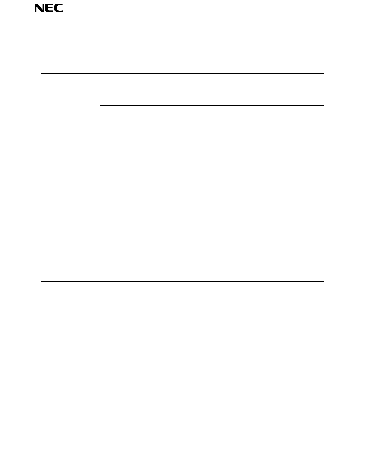
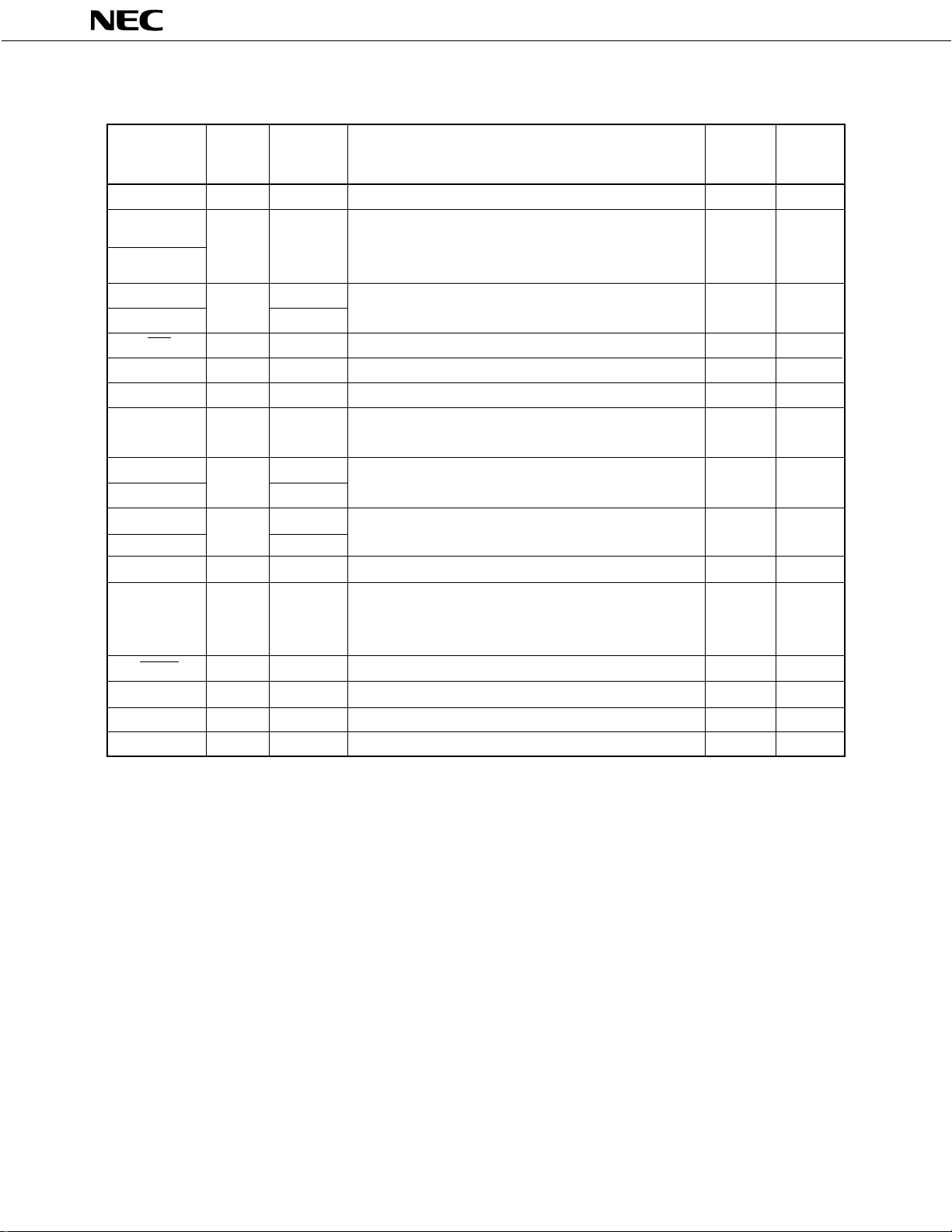
FUNCTIONAL OUTLINE
Item Specifications
Number of Basic Instructions 43
Minimum Instruction Changeable in three steps: 0.95 µs, 1.91 µs, and 15.3 µs at 4.19 MHz
Execution Time
ROM 8064 × 8 bits (µPD75108), 6016 × 8 bits (µPD75106), 4096 × 8 bits (µPD75104)
Internal Memory
General-Purpose Register 4 bits × 8 × 4 banks (memory mapped)
RAM 512 × 4 bits (µPD75108), 320 × 4 bits (µPD75106, 75104)
Accumulator
I/O Port
Timer/Counter
Serial Interface • LSB first/MSB first mode selectable
Vector Interrupt External: 3, Internal: 4
Test Input External: 2
Standby • STOP and HALT modes
Instruction Set
Three accumulators selectable according to the bit length of manipulated data:
• 1-bit accumulator (CY), 4-bit accumulator (A), and 8-bit accumulator (XA)
58 port pins
• CMOS input pins: 10
• CMOS I/O pins (can directly drive LEDs): 32
• Medium voltage N-ch open-drain I/O pins: 12
(can directly drive LEDs. Pull-up resistor can be connected to each bit)
• Comparator input pins (4-bit accuracy): 4
• 8-bit timer/event counter × 2
• 8-bit basic interval timer (can be used as watchdog timer)
• 8 bits
• Two transfer modes (transfer/reception and reception only modes)
• Various bit manipulation instructions (set, reset, test, Boolean operation)
• 8-bit data transfer, compare, operation, increment, and decrement
• 1-byte relative branch instructions
• GETI instruction constituting 2 or 3-byte instruction with 1 byte
Others
Package
• Power-ON reset circuit (mask option)
• Bit manipulation memory (bit sequential buffer: 16 bits)
• 64-pin plastic shrink DIP (750 mil)
• 64-pin plastic QFP (14 × 20 mm)
3
Page 4

µ
PD75104, 75106, 75108
CONTENTS
1. PIN CONFIGURATION (TOP VIEW)............................................................................................... 6
2. BLOCK DIAGRAM ........................................................................................................................... 8
3. PIN FUNCTIONS.............................................................................................................................. 9
3.1 PORT PINS............................................................................................................................................. 9
3.2 PINS OTHER THAN PORTS ................................................................................................................. 10
3.3 PIN INPUT/OUTPUT CIRCUITS ........................................................................................................... 11
3.4 RECOMMENDED PROCESSING OF UNUSED PINS .......................................................................... 12
3.5 NOTES ON USING THE P00/INT4, AND RESET PINS ...................................................................... 13
4. MEMORY CONFIGURATION .......................................................................................................... 14
5. PERIPHERAL HARDWARE FUNCTIONS........................................................................................ 20
5.1 PORTS .................................................................................................................................................... 20
5.2 CLOCK GENERATOR CIRCUIT ............................................................................................................ 21
5.3 CLOCK OUTPUT CIRCUIT .................................................................................................................... 22
5.4 BASIC INTERVAL TIMER ..................................................................................................................... 23
5.5 TIMER/EVENT COUNTER ..................................................................................................................... 23
5.6 SERIAL INTERFACE .............................................................................................................................. 25
5.7 PROGRAMMABLE THRESHOLD PORT (ANALOG INPUT PORT) .................................................... 27
5.8 BIT SEQUENTIAL BUFFER .... 16 BITS ............................................................................................... 28
5.9 POWER-ON FLAG (MASK OPTION) .................................................................................................... 28
6. INTERRUPT FUNCTIONS................................................................................................................ 28
7. STANDBY FUNCTIONS .................................................................................................................. 30
8. RESET FUNCTION........................................................................................................................... 31
9. INSTRUCTION SET ......................................................................................................................... 34
4
Page 5

µ
PD75104, 75106, 75108
10. APPLICATION EXAMPLES .............................................................................................................. 43
10.1 VTR SYSTEM CONTROLLER ............................................................................................................... 43
10.2 VTR CAMERA ........................................................................................................................................ 43
10.3 COMPACT DISC PLAYER ..................................................................................................................... 44
10.4 AUTOMOBILE APPLICATIONS (TRIP COMPUTER)............................................................................ 44
10.5 PUSHBUTTON TELEPHONE ................................................................................................................ 45
10.6 DISPLAY PAGER ................................................................................................................................... 45
10.7 PLAIN PAPER COPIER (PPC) ............................................................................................................... 46
10.8 PRINTER CONTROLLER ....................................................................................................................... 46
11. MASK OPTION SELECTION ........................................................................................................... 47
12. ELECTRICAL SPECIFICATIONS ...................................................................................................... 48
13. CHARACTERISTIC DATA ................................................................................................................ 57
14. PACKAGE DRAWINGS ................................................................................................................... 62
15. RECOMMENDED SOLDERING CONDITIONS ............................................................................... 65
APPENDIX A. FUNCTIONAL DIFFERENCES AMONG PRODUCTS IN µPD751XX SERIES ......... 66
APPENDIX B. DEVELOPMENT TOOLS .............................................................................................. 67
APPENDIX C. RELATED DOCUMENTS .............................................................................................. 68
5
Page 6
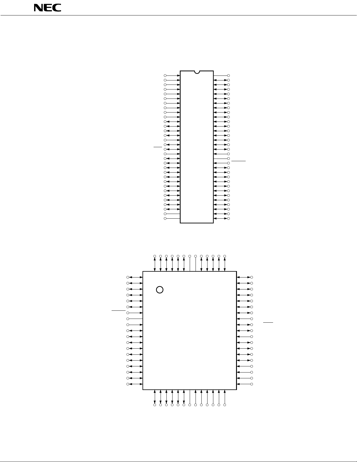
1. PIN CONFIGURATION (Top View)
P13/INT3 1
V32
V64
33
SS
µ
PD75104CW-
PD75106CW-
PD75108CW-
×××
×××
×××
P12/INT2
P11/INT1
P10/INT0
PTH03
PTH02
PTH01
PTH00
TI0
TI1
P23
P22/PCL
2
3
4
5
6
7
8
9
10
11
12
P21 PTO1 13
P20 PTO0 14
P9063
P9162
P9261
P9360
P8059
P8158
P8257
P8356
P7055
P7154
P7253
P7352
P6051
P03/SI 15 P6150
P02/SO 16 P6249
P01/SCK 17 P6348
P00/INT4 18 X147
P123 19 X246
P122 20 RESET45
P121 21 P5044
P120 22 P5143
P133 23 P5242
P132 24 P5341
P131 25 P4040
P130 26 P4139
P143 27 P4238
P142 28 P4337
P141 29 P3036
P140 30 P3135
NC 31 P3234
DD
µ
µ
P33
51 P1311P41
64
P42
P43
P30
P31
P32
P33VNC
P140
P141
P142
P143
P130
63 62 61 60 59 58 57 56 55 54 53 52
DD
20 21 22 23 24 25 26 27 28 29 30 31 32
P81
P80
P93
P92
P91
P90
V
P13/INT3
P12/INT2
P11/INT1
P10/INT0
PTH03
PTH02
SS
µ
PD75104GF-
PD75106GF-
PD75108GF-
×××
×××
×××
µ
µ
-3BE
-3BE
-3BE
50 P1322P40
49 P1333P53
48 P1204P52
47 P1215P51
46 P1226P50
45 P1237RESET
44 P00/INT48X2
43 P01/SCK9X1
42 P02/SO10P63
41 P03/SI11P62
40 P20/PTO012P61
39 P21/PTO113P60
38 P22/PCL14P73
37 P2315P72
36 TI116P71
35 TI017P70
34 PTH0018P83
33 PTH0119P82
• 64-Pin Plastic Shrink DIP (750 mil)
µ
PD75104, 75106, 75108
• 64-Pin Plastic QFP (14 × 20 mm)
6
Page 7

µ
PD75104, 75106, 75108
Pin names
P00-P03 : Port 0 SCK : Serial Clock Input/Output
P10-P13 : Port 1 SO : Serial Output
P20-P23 : Port 2 SI : Serial Input
P30-P33 : Port 3 PTO0, PTO1 : Timer Output
P40-P43 : Port 4 PCL : Clock Output
P50-P53 : Port 5 PTH00-PTH03 : Comparator Input
P60-P63 : Port 6
P70-P73 : Port 7 INT2, INT3 : External Test Input
P80-P83 : Port 8 TI0, TI1 : Timer Input
P90-P93 : Port 9 X1, X2 : Clock Oscillation Pin
P120-P123 : Port 12 RESET : Reset Input
P130-P133 : Port 13 NC : No Connection
P140-P143 : Port 14
INT0, INT1, INT4 : External Vector Interrupt Input
7
Page 8
8
2. BLOCK DIAGRAM
BIT SEQ.
BUFFER (16)
PORT 0
PORT 2
4
4
4
P00 - P03
P10 - P13PORT 1
P20 - P23
TI0
PTO0/P20
BASIC
INTERVAL
TIMER
INTBT
TIMER/EVENT
COUNTER
#0
INTT0
PROGRAM
COUNTER*
ALU
CY SP (8)
BANK
TI1
PTO1/P21
SI/P03
SO/P02
SCK/P01
INT0/P10
INT1/P11
INT2/P12
INT3/P13
INT4/P00
PTH00-PTH03 4
TIMER/EVENT
COUNTER
#1
INTT1
SERIAL
INTERFACE
INTSIO
INTERRUPT
CONTROL
PROGRAMMABLE
THRESHOLD
PORT #0
*: 13 bits: PD75106, 75108
µ
µ
12 bits: PD75104
ROM
PROGRAM
MEMORY
×
8064 8BITS
µ
: PD75108
×
6016 8BITS
µ
: PD75106
×
4096 8BITS
µ
: PD75104
N
f /2
XX
CLOCK
OUTPUT
CONTROL
PCL/P22 X1 X2 V
CLOCK
DIVIDER
DECODE
AND
CONTROL
CLOCK
GENERATOR
STAND BY
CONTROL
GENERAL REG.
RAM
DATA MEMORY
×
512 4BITS
µ
: PD75108
×
320 4BITS
µ
: PD75106, 75104
CPU CLOCK
Φ
DDVSS
RESET
PORT 3
PORT 4
PORT 5
PORT 6
PORT 7
PORT 8
PORT 9
PORT 12
PORT 13
PORT 14
4
P30 - P33
4
P40 - P43
P50 - P53
4
4
P60 - P63
4
P70 - P73
P80 - P83
4
4
P90 - P93
P120 - P123
4
4
P130 - P133
4
P140 - P143
µ
PD75104, 75106, 75108
Page 9
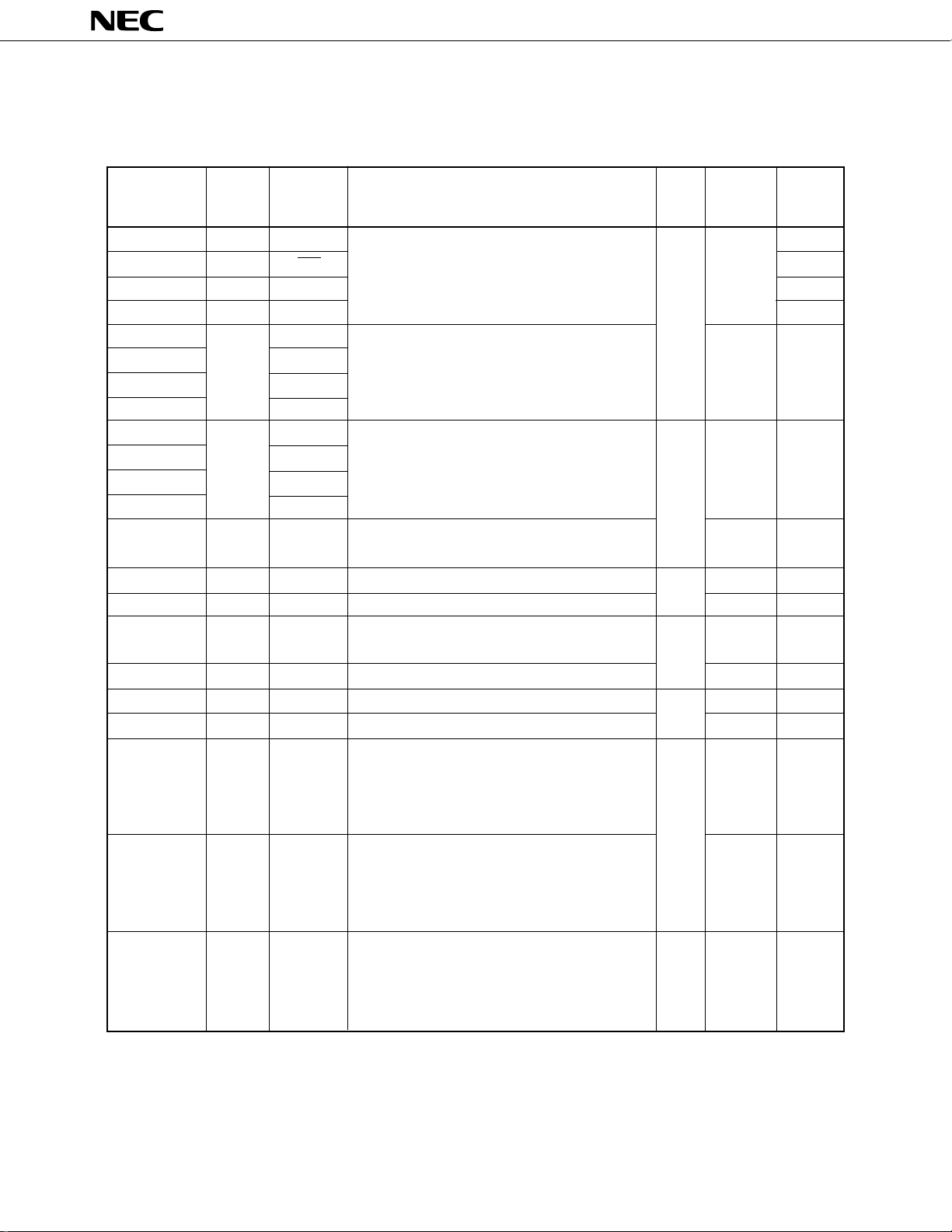
3. PIN FUNCTIONS
3.1 PORT PINS
µ
PD75104, 75106, 75108
Pin Name I/O
Shared with:
Function At Reset Circuit
8-Bit
I/O
P00 Input INT4 B
P01 I/O SCK F
P02 I/O SO E
P03 Input SI B
P10 INT0
P11 INT1
P12 INT2
Input 4-bit input port (PORT 1) Input B
4-bit input port (PORT 0) Input
x
P13 INT3
3
P20*
3
P21*
3
P22*
3
P23*
P30-P33*
P40-P43*
P50-P53*
P60-P63*
P70-P73*
P80-P83*
P90-P93*
I/O 4-bit I/O port (PORT 2) Input E
3
I/O — Input E
3
I/O — 4-bit I/O port (PORT 4) Input E
3
I/O — 4-bit I/O port (PORT 5) Input E
3
I/O — Input E
3
I/O 4-bit I/O port (PORT 7) Input E
3
I/O — 4-bit I/O port (PORT 8) Input E
3
I/O — 4-bit I/O port (PORT 9) Input E
PTO0
PTO1
PCL
—
x
4-bit programmable I/O port (PORT 3)
Can be specified for input or output bitwise.
o
4-bit programmable I/O port (PORT 6)
Can be specified for input or output bitwise. o
o
4-bit N-ch open-drain I/O port (PORT 12)
P120-P123*
P130-P133*
3
3
I/O —
I/O —
Built-in pull-up resistors can be specified in bit
units by mask option.
Open-drain withstanding voltage: 12 V
4-bit N-ch open-drain I/O port (PORT 13)
Built-in pull-up resistors can be specified in bit
units by mask option.
Input*
o
Input*
Open-drain withstanding voltage: 12 V
4-bit N-ch open-drain I/O port (PORT 14)
P140-P143*
3
I/O — – Input*
Built-in pull-up resistors can be specified in bit
units by mask option.
Open-drain withstanding voltage: 12 V
I/O
1
TYPE*
2
M
2
M
2
M
*1: Circles indicate Schmitt trigger input pins.
2: With drain open: high impedance
With pull-up resistor connected: high level
3: Can directly drive LEDs.
9
Page 10
µ
PD75104, 75106, 75108
3.2 PINS OTHER THAN PORTS
Pin Name I/O
PTH00-PTH03 Input — 4-bit variable threshold voltage analog input port — N
TI0 External event pulse inputs for timer/event counter.
TI1
PTO0 P20
PTO1 P21
SCK I/O P01 Serial clock I/O Input F
SO I/O P02 Serial data output Input E
SI Input P03 Serial data input Input B
INT4 Input P00 Input B
INT0 P10 Edge-detected vectored interrupt inputs (valid
INT1 P11 edge selectable)
INT2 P12
INT3 P13
PCL I/O P22 Clock output Input E
X1, X2 — — Input external clock to X1, and signal in reverse phase — —
RESET Input — System reset input (low level active type) — B
2
NC*
VDD — — Positive power supply — —
VSS ——GND ——
Input — Also serves as edge-detected vector interrupt input. — B
Input Input B
Input Edge-detected testable inputs (rising edge detected) Input B
Shared with:
1-bit input also possible.
I/O Outputs for timer/event counter Input E
Edge-detected vectored interrupt input (both rising and
falling edges detected)
Crystal/ceramic system clock oscillator connections.
with X1 to X2.
— — No Connection — —
Function At Reset Circuit
I/O
TYPE*
1
*1: Circles indicate Schmitt trigger input pins.
2: Connect the NC pin directly to the V
10
DD pin when
µ
PD75P108B and a printed circuit board are shared.
Page 11
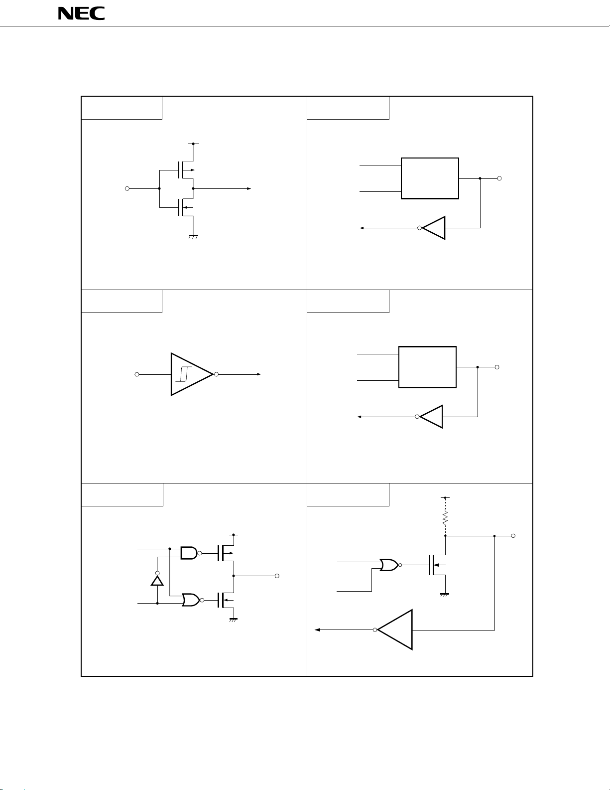
µ
3.3 PIN INPUT/OUTPUT CIRCUITS
The following shows a simplified input/output circuit diagram for each pin of the
PD75104, 75106, 75108
µ
PD75108.
TYPE A
DD
V
IN
Input buffer of CMOS standard
TYPE B
IN
P–ch
N–ch
TYPE E
data
Type D
output
disable
Type A
I/O circuit consisting of Type D push-pull output circuit
and Type A input buffer
IN/OUT
TYPE F
data
Type D
output
disable
IN/OUT
Schmitt trigger input with hysteresis characteristics
TYPE D
V
DD
data
output
disable
Push – pull output that can be set in a output
high– impedance state (both P –ch and N –ch are off)
P-ch
OUT
N-ch
Type B
I/O circuit consisting of Type D push-pull output and Type
B Schmitt trigger input
V
P.U.R.
DD
N-ch
(+12 V
withstand)
data
output
disable
TYPE M
Medium-voltage input
buffer (+12 V withstand)
P.U.R.: Pull-Up Resistor
(mask option)
IN/OUT
11
Page 12
TYPE N
Comparator
IN +
–
REF
V (threshold voltage)
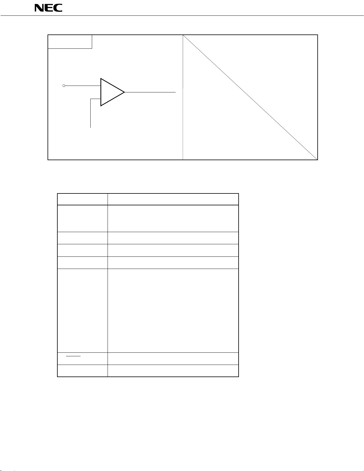
3.4 RECOMMENDED PROCESSING OF UNUSED PINS
µ
PD75104, 75106, 75108
Pin Recommended connections
PTH00-PTH03
TI0 Connect to VSS or VDD
TI1
P00 Connect to VSS
P01-P03 Connect to VSS or VDD
P10-P13 Connect to VSS
P20-P23
P30-P33
P40-P43
P50-P53
P60-P63 Input: Connect to VSS or VDD
P70-P73
P80-P83 Output: Open
P90-P93
P120-P123
P130-P133
P140-P143
RESET*
NC*
1
2
Connect to VDD
Open
12
*1: Connect this pin to the VDD pin only when a power-ON reset circuit
is provided as a mask option.
2: Connect the NC pin to the V
DD pin when
µ
PD75P108 and a printed
circuit board are shared.
Page 13
µ
PD75104, 75106, 75108
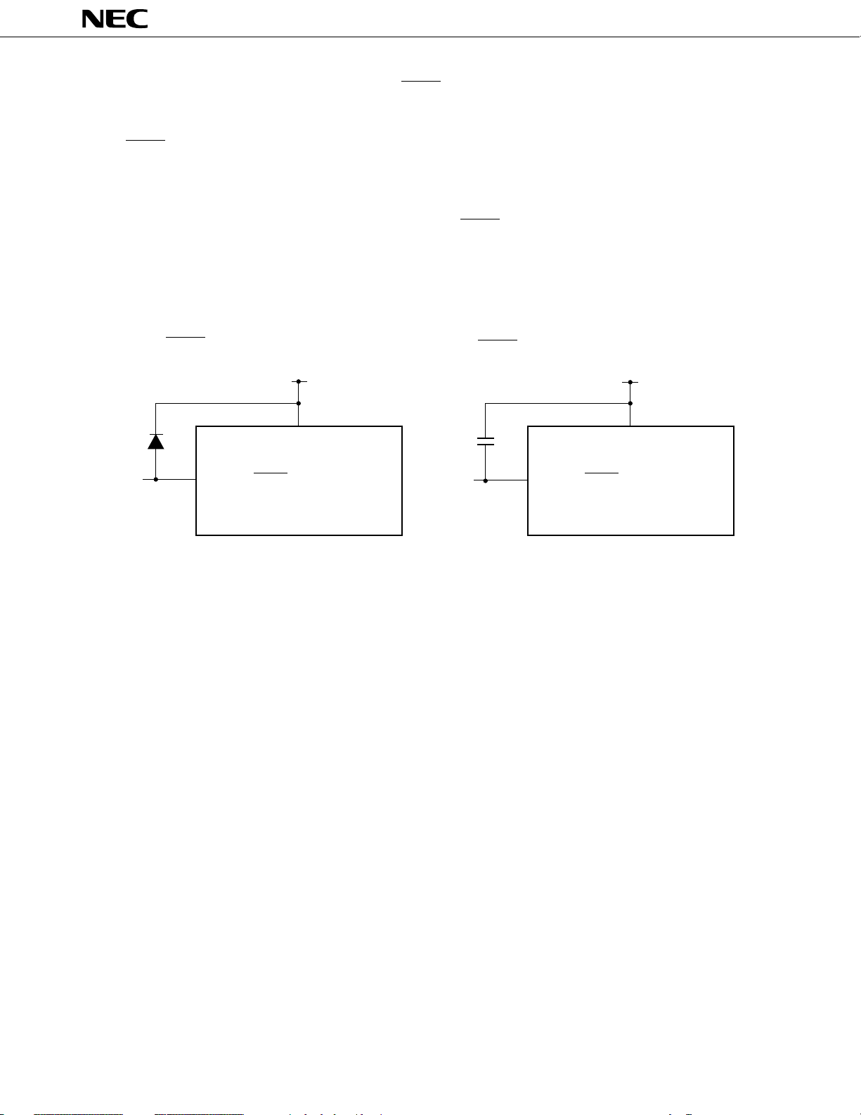
3.5 NOTES ON USING THE P00/INT4, AND RESET PINS
In addition to the functions described in Sections 3.1 and 3.2, an exclusive function for setting the test mode,
µ
in which the internal fuctions of the
RESET
and
If a voltage exceeding V
even when the
µ
PD75108 will enter the test mode, and this will cause problems for normal operation.
As an example, if the wiring to the P00/INT4 pin or the
and the above montioned problem may occur.
Therefore, all wiring to these pins must be made short enough to not pick up stray noise. If noise cannot
be avoided, suppress the noise using a capacitor or diode as shown in the figure below.
pins.
DD is applied to either of these pins, the
µ
PD75108 is in normal operation, if noise exceeding the VDD is input into any of these pins, the
PD75108 are tested (solely used for IC tests), is provided to the P00/INT4
µ
PD75108 is put into test mode. Therefore,
RESET
pin is long, stray noise may be picked up
• Connect a diode across P00/INT4 and
RESET
, and VDD.
VDD
VDD
P00/INT4, RESET
• Connect a capacitor across P00/INT4 and
, and VDD.
RESET
VDD
VDD
P00/INT4, RESET
13
Page 14

µ
PD75104, 75106, 75108
4. MEMORY CONFIGURATION
• Program memory (ROM) ... 8064 × 8 bits (0000H-1F7FH) : µPD75108
... 6016 × 8 bits (0000H-177FH) :
... 4096 × 8 bits (0000H-0FFFH) :
• 0000H, 0001H : Vector table to which address from which program is started is written after reset
• 0002H-000BH: Vector table to which address from which program is started is written after interrupt
• 0020H-007FH: Table area referenced by GETI instruction
• Data memory (RAM)
µ
• Data area ....512 × 4 bits (000H–1FFH):
320 × 4 bits (000H-13FH) :
• Peripheral hardware area .... 128 × 4 bits (F80H–FFFH)
PD75108
µ
PD75106, 75104
µ
PD75106
µ
PD75104
14
Page 15
(a) µPD75108
µ
PD75104, 75106, 75108
Address
0000H
0002H
0004H
0006H
0008H
000AH
765
MBE RBE 0
MBE RBE 0
MBE RBE 0
MBE RBE 0
MBE RBE 0
MBE RBE 0
Internal reset start address (upper 5 bits)
Internal reset start address (lower 8 bits)
INTBT/INT4 start address (upper 5 bits)
INTBT/INT4 start address (lower 8 bits)
INT0/INT1 start address (upper 5 bits)
INT0/INT1 start address (lower 8 bits)
INTSIO start address (upper 5 bits)
INTSIO start address (lower 8 bits)
INTT0 start address (upper 5 bits)
INTT0 start address (lower 8 bits)
INTT1 start address (upper 5 bits)
INTT1 start address (lower 8 bits)
0
CALLF
! faddr
instruction
entry
address
BRCB
! caddr
instruction
branch
address
CALL ! addr
instruction
subroutine
entry address
BR ! addr
instruction
branch address
0020H
007FH
0080H
07FFH
0800H
0FFFH
1000H
1F7FH
GETI instruction reference table
Fig. 4-1 Program Memory Map (1/3)
BR $addr
instruction
relational
branch address
(–15 to –1,
+2 to +16)
Branch destination
address and
subroutine entry
address for
GETI instruction
BRCB ! caddr
instruction
branch address
Remarks: In addition to the above addresses, program can be branched to addresses specified by the PC
with the contents of its lower 8 bits changed by BR PCDE or BR PCXA instruction.
15
Page 16
(b) µPD75106
µ
PD75104, 75106, 75108
Address
0000H
0002H
0004H
0006H
0008H
000AH
765
MBE RBE 0
MBE RBE 0
MBE RBE 0
MBE RBE 0
MBE RBE 0
MBE RBE 0
Internal reset start address (upper 5 bits)
Internal reset start address (lower 8 bits)
INTBT/INT4 start address (upper 5 bits)
INTBT/INT4 start address (lower 8 bits)
INT0/INT1 start address (upper 5 bits)
INT0/INT1 start address (lower 8 bits)
INTSIO start address (upper 5 bits)
INTSIO start address (lower 8 bits)
INTT0 start address (upper 5 bits)
INTT0 start address (lower 8 bits)
INTT1 start address (upper 5 bits)
INTT1 start address (lower 8 bits)
0
CALLF
! faddr
instruction
entry
address
BRCB
! caddr
instruction
branch
address
CALL ! addr
instruction
subroutine
entry address
BR ! addr
instruction
branch address
0020H
007FH
0080H
07FFH
0800H
0FFFH
1000H
177FH
GETI instruction reference table
Fig. 4-1 Program Memory Map (2/3)
BR $addr
instruction
relational
branch address
(–15 to +16)
Branch destination
address and
subroutine entry
address for
GETI instruction
BRCB ! caddr
instruction
branch address
Remarks: In addition to the above addresses, program can be branched to addresses specified by the PC
with the contents of its lower 8 bits changed by BR PCDE or BR PCXA instruction.
16
Page 17
(c) µPD75106
µ
PD75104, 75106, 75108
Address
000H
002H
004H
006H
008H
00AH
020H
07FH
080H
765
MBE RBE 0
MBE RBE 0
MBE RBE 0
MBE RBE 0
MBE RBE 0
MBE RBE 0
4
0
Internal reset start address (upper 4 bits)
Internal reset start address (lower 8 bits)
INTBT/INT4 start address (upper 4 bits)
0
INTBT/INT4 start address (lower 8 bits)
INT0/INT1 start address (upper 4 bits)
0
INT0/INT1 start address (lower 8 bits)
INTSIO start address (upper 4 bits)
0
INTSIO start address (lower 8 bits)
INTT0 start address (upper 4 bits)
0
INTT0 start address (lower 8 bits)
INTT1 start address (upper 4 bits)
0
INTT1 start address (lower 8 bits)
GETI instruction reference table
0
CALLF
! faddr
instruction
entry
address
BRCB ! caddr
instruction
branch address
CALL ! addr
instruction
subroutine
entry address
Branch destination
address and
subroutine entry
address for
GETI instruction
BR $addr
instruction
relational
branch address
(–15 to +16)
7FFH
800H
FFFH
Fig. 4-1 Program Memory Map (3/3)
Remarks: In addition to the above addresses, program can be branched to addresses specified by the PC
with the contents of its lower 8 bits changed by BR PCDE or BR PCXA instruction.
17
Page 18
(a) µPD75108
µ
PD75104, 75106, 75108
Stack area
Data memory
Static RAM
(512× 4)
Peripheral hardware area
General-purpose
register area
000H
01FH
0FFH
100H
1FFH
F80H
FFFH
Data memory
(32 × 4)
256× 4
256× 4 Bank 1
Not provided
128× 4
Memory bank
Bank 0
Bank 15
Fig. 4-2 Data Memory Map(1/2)
18
Page 19
(b) µPD75106, 75104
µ
PD75104, 75106, 75108
General-
Stack area
purpose
Static RAM
(320× 4)
Peripheral hardware area
General-purpose
register area
000H
01FH
0FFH
100H
13FH
F80H
FFFH
Data memory
(32 × 4)
256× 4
× 4
64
Not provided
128× 4
Memory bank
Bank 0
Bank 1
Bank 15
Fig. 4-2 Data Memory Map(2/2)
19
Page 20
5. PERIPHERAL HARDWARE FUNCTIONS
5.1 PORTS
I/O ports are classified into the following 3 kinds:
• CMOS input (PORT0, 1) : 8
• CMOS input/output (PORT2, 3, 4, 5, 6, 7, 8, 9): 32
N-ch open-drain input/output (PORT12, 13, 14) :12
•
Total : 52
Table 5-1 Port Function
µ
PD75104, 75106, 75108
Port
(Symbol)
PORT0
PORT1
PORT3
PORT6
PORT2
PORT4
PORT5
PORT7
PORT8
PORT9
PORT12
PORT13
PORT14
Function
4-bit input
4-bit I/O*
4-bit I/O*
(N-ch open- drain.
12V)
*: Can directly drive LED.
Operation and Features
Can always be read or tested regardless of operation mode of shared pin
Can be set in input or output mode bitwise
Can be set in input or output mode in units of 4 bits.
Ports 4 and 5, 6 and 7, 8 and 9 can be used in pairs
to input or output 8-bit data
Can be set in input or output mode in units of 4 bits.
Ports 12 and 13 can be used in pairs to input or
output 8-bit data
Remarks
Shared with SI, SO, SCK, and
INT0 to 4 pins
—
Port 2 pins are shared with
PTO0, PTO1, and PCL pins
Each bit can be connected to
pull-up resistor by mask option
20
Page 21
µ
PD75104, 75106, 75108
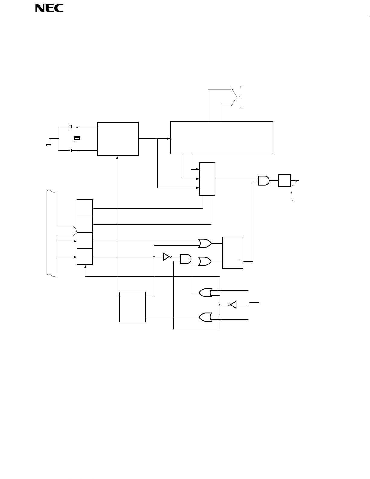
5.2 CLOCK GENERATOR CIRCUIT
The clock generator circuit generates clocks to control CPU operation modes by supplying clocks to the CPU and
peripheral hardware. In addition, this circuit can change the instruction execution time.
µ
• 0.95
s/1.91 µs/15.3 µs (operating at 4.19 MHz)
· Basic interval timer (BT)
· Clock output circuit
· Timer/event counter
· Serial interface
4
Internal bus
HALT*
STOP*
PCC
PCC0
PCC1
PCC2
PCC3
Clears
PCC2,
PCC3
X1
System clock
generator
circuit
X2
Oscillation
stops
STOP F/F
Q
S
XX
f or
f
X
1/2 1/16
1/8 to 1/4096
Frequency civider
Selector
HALT F/F
S
RQ
Frequency
divider
1/4
Wait release signal from BT
RES (internal reset) signal
Φ
· CPU
· Clock output
circuit
*: Execution of the instruction
Remarks 1: f
XX= Crystal/ceramic oscillator
2: f
X = External clock frequency
3: PCC: Processor clock control register
4: One clock cycle (t
characteristics in 12. ELECTRICAL SPECIFICATIONS.
R
CY) of Φ is one machine cycle of an instruction. For tCY, refer to AC
Standby release signal from
interrupt control circuit
Fig. 5-1 Clock Generator Block Diagram
★
21
Page 22
µ
PD75104, 75106, 75108
5.3 CLOCK OUTPUT CIRCUIT
The clock output circuit outputs clock pulse from the P22/PCL pin. This clock output circuit is used to output
clock pulses to the remote control output, peripheral LSIs, etc.
• Clock output (PCL) : Φ, 524, 262 kHz (operating at 4.19 MHz)
From the
clock
generator
Φ
Output
3
X
/2
X
f
Selector
buffer
4
fX/2
X
CLOM3 CLOM2 CLOM1 CLOM0 CLOM
4
Fig. 5-2 Clock Output Circuit Configuration
Internal bus
P22 output
latch
Bit 2 of PMGBPORT2.2
Port 2 input/
output mode
specification
bit
PCL/P22
22
Page 23

µ
PD75104, 75106, 75108
5.4 BASIC INTERVAL TIMER
The basic interval timer has these functions:
• Interval timer operation which generates a reference time interrupt
• Watchdog timer application which detects a program runaway
• Selects the wait time for releasing the standby mode and counts the wait time
• Reads out the count value
From the
clock generator
5
f
X
/2
X
Clear
Clear
7
X
fX/2
MPX
9
X
fX/2
12
X
fX/2
3
BTM3 BTM2 BTM1 BTM0 BTM
SET1*
Remarks
4
: *: Instruction execution
Basic interval timer
(8-bit frequency divider circuit)
BT
Wait release signal
for standby release
8
Internal bus
Set
signal
BT
interrupt
request flag
IRQBT
Fig. 5-3 Basic Interval Timer Configuration
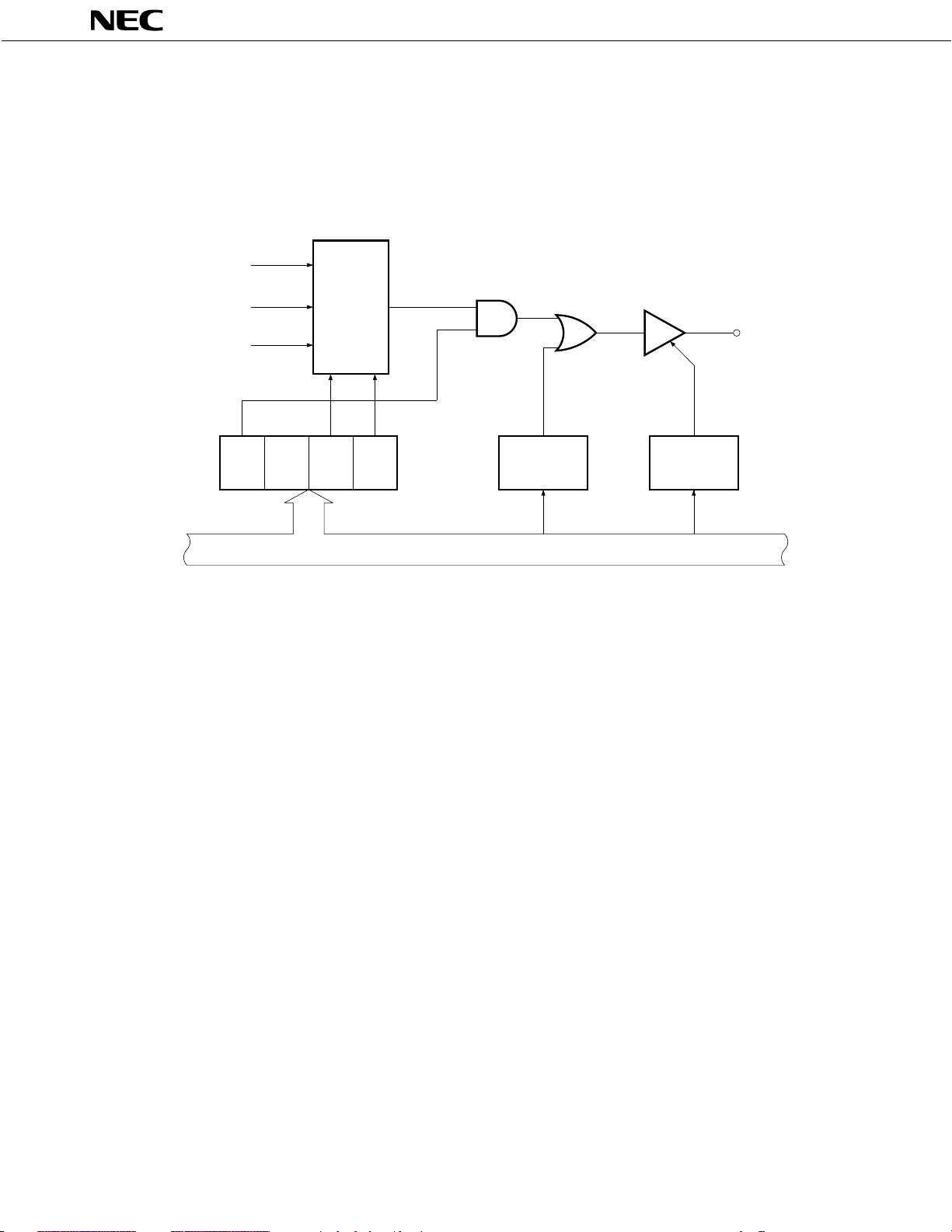
5.5 TIMER/EVENT COUNTER
µ
PD75108 contains two channels of timer/event counters.
These two channels are almost identical in terms of configuration and function except the count pulse (CP) that
can be selected and the function to supply clocks to the serial interface.
The functions of the timer/event counter include:
Vector
interrupt
request
signal
• Programmable interval timer operation
• Output of square wave at an arbitrary frequency to PTOn pin
• Event counter operation
• Input of TIn pin signal as external interrupt input signal
• Dividing TIn pin input by N to output to PTOn pin (frequency divider operation)
• Supply of serial shift clock to serial interface circuit (channel 0 only)
• Reading counting status
23
Page 24

24
TIn
Input buffer
TIn
From
clock
generator
circuit
Internal bus
SET1*
888
MPX
Timer operation start
TMn TMODn
Modulo register (8)TMn7 TMn6 TMn5 TMn4 TMn3 TMn2 TMn1 TMn0
8
Coincidence
Comparator (8)
8
CP
Count register (8)
Clear
RES
Tn
TOUT
F/F
TOFn
TOEn TOn PORT2.n Bit 2 of PGMB
To
enable
flag
To
selector
TMn1 TMn0
P2n
output
latch
Edge
detector
circuit
Port 2
I/O
mode
Output
buffer
IRQTn set
signal
IRQTn clear
signal
To serial
interface
(channel 0 only)
P2n/PTOn
µ
PD75104, 75106, 75108
Remarks:
* indicates the instruction execution.
Fig. 5-4 Timer/Event Counter Block Diagram (n = 0, 1)
Page 25

5.6 SERIAL INTERFACE
µ
PD75108 is equipped with clock 8-bit serial interface that operates in the following two modes:
The
• Operation stop mode
• Three-line serial I/O mode
µ
PD75104, 75106, 75108
25
Page 26

26
Internal bus
P03/SI
P02/SO
P01/SCK
8
SIO0
Shift register (8)
*: "SET1" indicates execution of the instruction.
8
Serial clock
counter (3)
QS
SIO7
Clear
R
SIO
Overflow
SET1*
8
SIOM7 SIOM6 SIOM5 SIOM4 SIOM3 SIOM2 SIOM1 SIOM0
Serial start
Φ
4
f /2
MPX
XX
10
f /2
XX
TOF0 (from timer channel 0)
SIOM
IRQSIO
set signal
IRQSIO
clear signal
µ
PD75104, 75106, 75108
Fig. 5-5 Serial Interface Block Diagram
Page 27

µ
PD75104, 75106, 75108
5.7 PROGRAMMABLE THRESHOLD PORT (ANALOG INPUT PORT)
µ
PD75108 is equipped with a 4-bit analog input port (consisting of PTH00 to PTH03 pins) whose threshold voltage
is programmable.
This programmable threshold port is configured as shown in Figure 5-6.
The threshold voltage (V
REF) can be changed in 16 steps (VDD × 0.5/16 – VDD × 15.5/16), and analog signals can be
directly input.
When V
REF is set to VDD × 7.5/16, the programmable threshold port can also be used as a digital signal input port.
Input buffer
PTH00
+
–
PTH01
PTH02
PTH03
1
2
1
2
+
–
+
–
Programmable threshold port
+
–
Operates
/stops
DD
V
R
R
R
REF
MPX
R
4
V
input latch (4)
PTH0
Internal bus
PTHM7
PTHM6
PTHM5
PTHM4
8
PTHM3
PTHM2
PTHM1
PTHM0
PTHM
Fig. 5-6 Programmable Threshold Port Configuration
27
Page 28

µ
PD75104, 75106, 75108
5.8 BIT SEQUENTIAL BUFFER .... 16 BITS
The bit sequential buffer is a data memory specifically provided for bit manipulation. With this buffer,
addresses and bit specifications can be sequentially up-dated in bit manipulation operation. Therefore, this
buffer is very useful for processing long data in bit units.
Address bit
L register
Remarks:
Symbol
L = F L = C L = B L = 8 L = 7 L = 4 L = 3 L = 0
For the pmem.@L addressing, the specification bit is shifted according to the L register.
FC3H FC2H FC1H FC0H
3210321032103210
BSB3 BSB2 BSB1 BSB0
DECS L
INCS L
Fig. 5-7 Bit Sequential Buffer Format
5.9 POWER-ON FLAG (MASK OPTION)
The power-ON flag (PONF) is set to only when the power-ON reset circuit operates and power-ON reset signal
has been generated (see Fig. 8-1).
The PONF flag is mapped at bit 0 of memory space address FD1H, and can be manipulated by a bit manipulation
instruction. However, it cannot be set by the SET1 instruction.
6. INTERRUPT FUNCTIONS
The µPD75108 has 7 different interrupt sources and can perform multiplexed interrupt processing with
priority assigned.
µ
In addition to that, the
The interrupt control circuit of the
• Hardware controlled vector interrupt function which can control whether or not to accept an interrupt by
using the interrupt enable flag (IExxx) and interrupt master enable flag (IME).
• The interrupt start address can be arbitrarily set.
• Multiplexed interrupt function that can specify priority by the interrupt priority selector register (IPS).
• Interrupt request flag (IRQxxx) test function (an interrupt generation can be confirmed by means of
software).
• Standby mode release (Interrupts to be released can be selected by the interrupt enable flag).
PD75108 is also provided with two types of edge detection testable inputs.
µ
PD75108 has these functions:
28
Page 29

Internal bus
INT4
/P00
INT0
/P10
INT1
/P11
INT2
/P12
INT3
/P13
22
IM1 IM0
INT
BT
Both edge
detection
circuit
Edge
detection
circuit
Edge
detection
circuit
INTSIO
INTT0
INTT1
Rising edge
detection
circuit
Falling edge
detection
circuit
9
IRQBT
IRQ4
IRQ0
IRQ1
IRQSIO
IRQT0
IRQT1
IRQ2
IRQ3
Interrupt
request flag
Interrupt enable flag (IE )×××
IME
IPS
Decoder
Priority control
circuit
24
IST
Vector table
address
generator
µ
PD75104, 75106, 75108
Standby
release signal
29
Fig. 6-1 Interrupt Control Block Diagram
Page 30

µ
PD75104, 75106, 75108
7. STANDBY FUNCTIONS
The µPD75108 has two different standby modes (STOP mode and HALT mode) to reduce the power
consumption of the microcomputer chip while waiting for program execution.
Table 7-1 Each Status in Standby Mode
STOP Mode
Setting Instruction STOP instruction HALT instruction
Clock Generator
circuit
Basic Interval
Timer
Operation
Status
Release Signal Interrupt request signal enabled by interrupt enable flag, or RESET input
Serial Interface
Timer/Event
Counter
Clock output
CPU Stops
circuit
Clock oscillation stops Only CPU clock Φ is stopped
Stops
Operates only when input of external
SCK or output of TO0 is selected as
serial clock (where external TI0 is input
to timer/event counter 0)
Operates only when TIn pin input
signal is specified as count clock
Stops
Operates (sets IRQBT at reference
time intervals)
Operates when serial clock other
than Φ is specified
Operates
Operates when clock other than CPU
clock Φ is used
Stops
HALT Mode
30
Page 31

8. RESET FUNCTION
µ
PD75104, 75106, 75108
The reset (
RES
) signal generator circuit is configured as shown in Figure 8-1.
RESET
SWB
Power-ON
reset
generator
circuit
SWA
Power-ON
flag (PONF)
Internal reset signal
(RES)
Execution of bit
manipulation
instruction*
Internal bus
*: PONF cannot be set to 1 by SET1 instruction.
Fig. 8-1 Reset Signal Generator Circuit
The Power-ON reset generator circuit generates an internal reset signal when the supply voltage rises. This pulse
can be used in three ways by specifying a mask option through SWA and SWB shown in Fig. 8-1. (Refer to 11. MASK
OPTION SELECTION.)
The reset operations performed by the Power-On reset circuit and the RESET input signal are illustrated in Figs.
8-2 and 8-3, respectively.
Supply voltage
0 V
Internal reset signal
(RES)
Internal reset operation
(approx. 31.3 ms: 4.19 MHz)
HALT mode Operation mode
*: The wait time does not include the time required after the
oscillation starts.
Fig. 8-2 Reset by Power-ON Reset Circuit
Wait*
RES
signal has been generated until the
31
Page 32

RESET input
Operation mode
or standby mode
(31.3 ms: 4.19 MHz)
Internal reset operation
µ
PD75104, 75106, 75108
Wait*
HALT mode Operation mode
*: The wait time does not include the time required after the
oscillation starts.
RES
signal has been generated until the
Fig. 8-3 Reset by RESET Signal
The status of each internal hardware device after the reset operation has been performed is shown in Table 8-
1.
32
Page 33

µ
PD75104, 75106, 75108
Table 8-1 Hardware Device Status After Reset
Hardware
Program Counter (PC) set to PC12-8,*1 and set to PC12-8,*1 and
Carry Flag (CY) Retained Undefined
Skip Flags (SK0-SK2) 0 0
PSW Interrupt Status Flags (IST0, 1) 0 0
Bank Enable Flags (MBE, RBE)
Stack Pointer (SP) Undefined Undefined
Data Memory (RAM) Retained*
General-Purpose Registers (X,A,H,L,D,E,B,C) Retained Undefined
Bank Selector Registers (MBS, RBS) 0, 0 0, 0
Basic interval timer
Timer/Event Counter
(n = 0, 1)
Serial Interface
Clock Generator Circuit,
Clock Output Circuit
Interrupt
Digital Port
Analog Port
Power-ON Flag (PONF) Retained 1 or undefined*
Bit Sequential Buffer (BSB0-BSB3) 0 0
Counter (BT) Undefined Undefined
Mode Register (BTM) 0 0
Counter (Tn) 0 0
Modulo Register (TMODn) FFH FFH
Mode Register (TMn) 0 0
TOEn, TOFn 0, 0 0, 0
Shift Register (SIO) Retained Undefined
Mode Register (SIOM) 0 0
Processor Clock Control Register 0 0
(PCC)
Clock Output Mode Register 0 0
(CLOM)
Interrupt Request Rlags Reset (0) Reset (0)
(IRQxxx)
Interrupt Enable Flags (IExxx) 0 0
Priority Selector Register (IPS) 0 0
INT0, 1 Mode Registers 0, 0 0, 0
(IM0, IM1)
Output Buffer OFF OFF
Output Latch Cleared (0) Cleared (0)
I/O Mode Registers 0 0
(PMGA, PMGB, PMGC)
PTH00-PTH03 Input Latches Undefined Undefined
Mode Register (PTHM) 0 0
RESET input during Power-ON Reset or RESET
standby mode Input during Operation
Lower 4 bits of program Lower 4 bits of program
memory address 000H are memory address 000H are
contents of address 001H contents of address 001H
are set to PC7-0. are set to PC7-0.
Bit 6 of program memory Bit 6 of program memory
address 000H is set in address 000H is set in
RBE, and bit 7 is set in RBE, and bit 7 is set in
MBE. MBE.
2
Undefined
2
*1: PC11-8 for µPD75104
2: Power-ON reset: 1
RESET
input during operation: undefined
Note: Data at data memory addresses 0F8H to 0FDH become undefined when the
RESET
signal has been input.
33
Page 34

µ
PD75104, 75106, 75108
9. INSTRUCTION SET
(1) Operand representation and description
Describe one or more operands in the operand field of each instruction according to the operand
representation and description methods of the instruction (for details, refer to RA75X Assembler Package
User's Manual - Language (EEU-730)). With some instructions, only one operand should be selected from
several operands. The uppercase characters, +, and – are keywords and must be described as is.
Describe an appropriate numeric value or label as immediate data.
The symbols in the register and flag symbols can be described as labels in the places of mem, fmem,
µ
pmem, and bit (for details, refer to
restricts the label that can be described.
Representation Description
reg X, A, B, C, D, E, H, L
reg1 X, B, C, D, E, H, L
rp XA, BC, DE, HL
rp1 BC, DE, HL
rp2 BC, DE
rp' XA, BC, DE, HL, XA', BC', DE', HL'
rp'1 BC, DE, HL, XA', BC', DE', HL'
rpa HL, HL+, HL–, DE, DL
rpa1 DE, DL
n4 4-bit immediate data or label
n8 8-bit immediate data or label
mem 8-bit immediate data or label*
bit 2-bit immediate data or label
fmem FB0H to FBFH,FF0H to FFFH immediate data or label
pmem FC0H to FFFH immediate data or label
addr
caddr 12-bit immediate data or label
faddr 11-bit immediate data or label
taddr 20H to 7FH immediate data (where bit0 = 0) or label
PORTn PORT0 - PORT9, PORT12 - PORT14
IExxx IEBT, IESIO, IET0, IET1, IE0 - IE4
RBn RB0 - RB3
MBn MB0, MB1, MB15
PD751XX Series User‘s Manual (IEM-922)). However, fmem and pmem
µ
PD75104 0000H to 0FFFH immediate data or label
µ
PD75106 0000H to 177FH immediate data or label
µ
PD75108 0000H to 1F7FH immediate data or label
34
*: Only even address can be described as mem for 8-bit data processing.
Page 35

(2) Legend of operation field
A : A register; 4-bit accumulator
B : B register; 4-bit accumulator
C : C register; 4-bit accumulator
D : D register; 4-bit accumulator
E : E register; 4-bit accumulator
H : H register; 4-bit accumulator
L : L register; 4-bit accumulator
X : X register; 4-bit accumulator
XA : Register pair (XA); 8-bit accumulator
BC : Register pair (BC); 8-bit accumulator
DE : Register pair (DE); 8-bit accumulator
HL : Register pair (HL); 8-bit accumulator
XA' : Expansion register pair (XA')
BC' : Expansion register pair (BC')
DE' : Expansion register pair (DE')
HL' : Expansion register pair (HL')
PC : Program counter
SP : Stack pointer
CY : Carry flag; or bit accumulator
PSW : Program status word
MBE : Memory bank enable flag
RBE : Register bank enable flag
PORTn : Port n (n = 0 - 9, 12 - 14)
IME : Interrupt mask enable flag
IPS : Interrupt priority selection register
IExxx : Interrupt enable flag
RBS : Register bank selection register
MBS : Memory bank selection register
PCC : Processor clock control register
.
(xx) : Contents addressed by xx
xxH : Hexadecimal data
: Delimiter of address and bit
µ
PD75104, 75106, 75108
35
Page 36

µ
PD75104, 75106, 75108
(3) Symbols in addressing area field
*1 MB = MBE . MBS
(MBS = 0, 1, 15)
*2 MB = 0
*3 MBE = 0 : MB = 0 (00H-7FH) Data memory
MBE = 1 : MB = MBS (MBS = 0, 1, 15)
*4 MB = 15, fmem = FB0H-FBFH,
*5 MB = 15, pmem = FC0H-FFFH
*6
µ
PD75104 addr = 0000H-0FFFH
µ
PD75106 addr = 0000H-177FH
µ
PD75108 addr = 0000H-1F7FH
*7 addr = (Current PC) – 15 to (Current PC) – 1
*8
µ
PD75104 caddr = 0000H-0FFFH (PC11 = 0) addressing
µ
PD75106 caddr = 0000H-0FFFH (PC12 = 0) or 1000H-177FH (PC12 = 1)
µ
PD75108 caddr = 0000H-0FFFH (PC12 = 0) or 1000H-1F7FH (PC12 = 1)
*9 faddr = 000H-7FFH
*10 taddr = 020H-07FH
MB = 15 (80H-FFH) addressing
FF0H-FFFH
(Current PC) + 2 to (Current PC) + 16 Program memory
Remarks • MB indicates memory bank that can be accessed.
• In *2, MB = 0 regardless of MBE and MBS.
• In *4 and *5, MB = 15 regardless of MBE and MBS.
• *6 to *10 indicate areas that can be addressed.
(4) Machine cycle field
In this field, S indicates the number of machine cycles required when an instruction having a skip
function skips. The value of S varies as follows:
• When no instruction is skipped ........................................................................ S = 0
• When 1-byte or 2-byte instruction is skipped................................................. S = 1
• When 3-byte instruction (BR ! adder or CALL ! adder) is skipped .............. S = 2
Note
: The GETI instruction is skipped in one machine cycle.
One machine cycle equals to one cycle of the CPU clock Φ, (= tCY), and can be changed in three steps
depending on the setting of the processor clock control register (PCC).
36
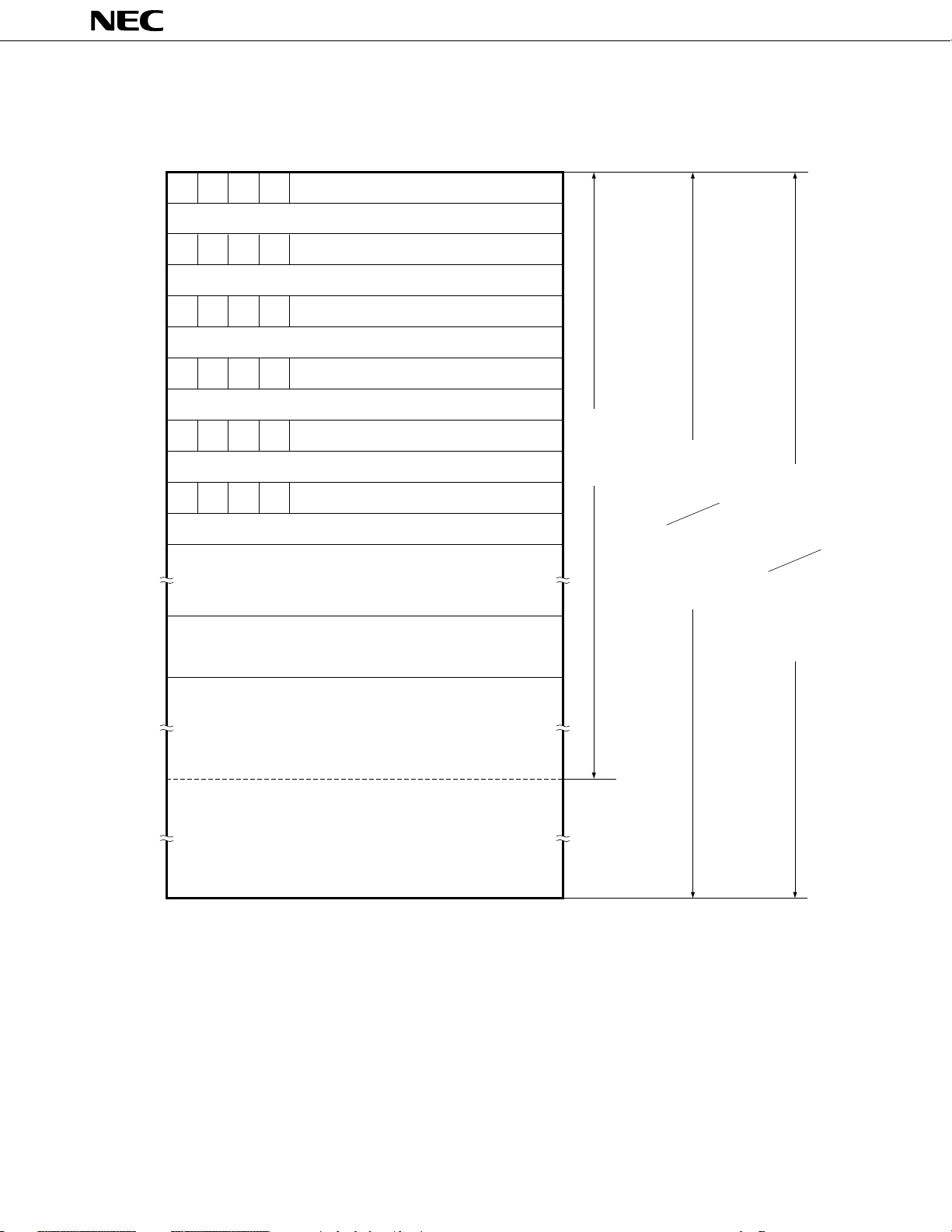
Page 37

µ
PD75104, 75106, 75108
Instruc- Mnetions monics Cyc- Area Conditions
Transfer MOV A, #n4 1 1 A ← n4 String effect A
XCH A, @HL 1 1 A ↔ (HL) *1
Table
Reference
MOVT XA, @PCDE 1 3 •µPD75104
Operand Bytes
reg1, #n4 2 2 reg1 ← n4
XA, #n8 2 2 XA ← n8 String effect A
HL, #n8 2 2 HL ← n8 String effect B
rp2, #n8 2 2 rp2 ← n8
A, @HL 1 1 A ← (HL) *1
A, @HL+ 1 2+S A ← (HL), then L ← L+1 *1 L = 0
A, @HL– 1 2+S A ← (HL), then L ← L–1 *1 L = FH
A, @rpa1 1 1 A ← (rpa1) *2
XA, @HL 2 2 XA ← (HL) *1
@HL, A 1 1 (HL) ← A*1
@HL, XA 2 2 (HL) ← XA *1
A,mem 2 2 A ← (mem) *3
XA, mem 2 2 XA ← (mem) *3
mem, A 2 2 (mem) ← A*3
mem, XA 2 2 (mem) ← XA *3
A, reg 2 2 A ← reg
XA, rp' 2 2 XA ← rp'
reg1, A 2 2 reg1 ← A
rp'1, XA 2 2 rp'1 ← XA
A, @HL+ 1 2+S A ↔ (HL), then L ← L+1 *1 L = 0
A, @HL– 1 2+S A ↔ (HL), then L ← L–1 *1 L = FH
A, @rpa1 1 1 A ↔ (rpa1) *2
XA, @HL 2 2 XA ↔ (HL) *1
A, mem 2 2 A ↔ (mem) *3
XA, mem 2 2 XA ↔ (mem) *3
A, reg1 1 1 A ↔ reg1
XA, rp' 2 2 XA ↔ rp'
XA, @PCXA 1 3 •µPD75104
Ma-
chine
les
Operation
XA ← (PC11-8+DE)ROM
•µPD75106, 75108
XA ← (PC12-8+DE)ROM
XA ← (PC11-8+XA)ROM
•µPD75106, 75108
XA ← (PC12-8+XA)ROM
Addressing Skip
37
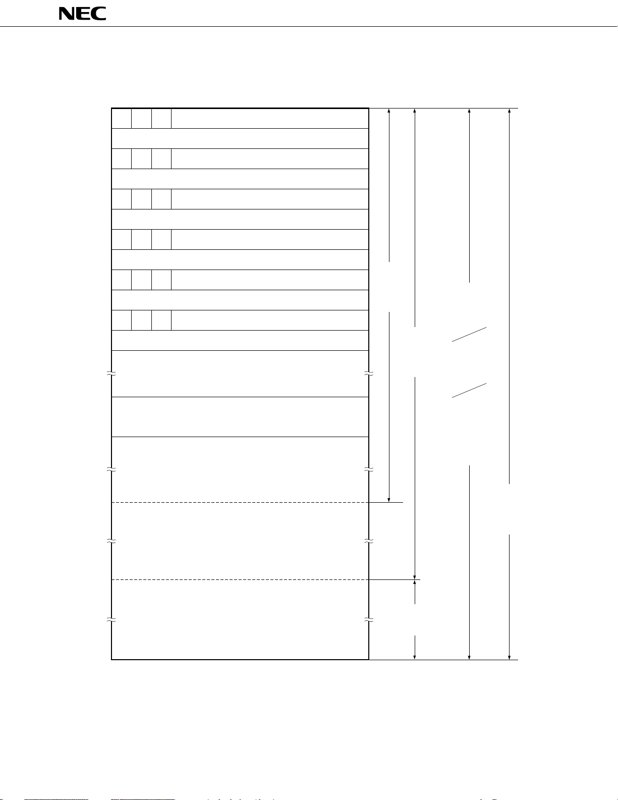
Page 38

µ
PD75104, 75106, 75108
Instruc- Mnetions monics Cyc- Area Conditions
Bit MOV1 CY,fmem.bit 2 2 CY ← (fmem.bit) *4
transfer CY,pmem.@L 2 2 CY ← (pmem7-2+L3-2.bit(L1-0)) *5
Arith- ADDS A, #n4 1 1+S A ← A+n4 carry
metic XA, #n8 2 2+S XA ← XA+n8 carry
opera- A, @HL 1 1+S A ← A+(HL) *1 carry
tion XA, rp’ 2 2+S XA ← XA+rp’ carry
ADDC A, @HL 1 1 A, CY ← A+(HL)+CY *1
SUBS A, @HL 1 1+S A ← A-(HL). *1 borrow
SUBC A, @HL 1 1 A, CY ← A-(HL)-CY *1
AND A, #n4 2 2 A ← A ∧ n4
OR A, #n4 2 2 A ← A ∨ n4
XOR A, #n4 2 2 A ← A ∨ n4
Accumulator
Manipulation
Incre- INCS reg 1 1+S reg ← reg+1 reg = 0
ment/ rp1 1 1+S rp1 ← rp1+1 rp1 = 00H
decre- @HL 2 2+S (HL) ← (HL)+1 *1 (HL) = 0
ment mem 2 2+S (mem) ← (mem)+1 *3 (mem) = 0
RORC A 1 1 CY ← A0, A3 ← CY, An-1 ← An
NOT A 2 2 A ← A
DECS reg 1 1+S reg ← reg-1 reg = FH
Operand Bytes
CY,@H+mem. 2 2 CY ← (H+mem3-0.bit) *1
bit
fmem.bit,CY 2 2 (fmem.bit) ← CY *4
pmem.@L,CY 2 2 (pmem7-2+L3-2.bit(L1-0)) ← CY *5
@H+mem.bit, 2 2 (H+mem3-0.bit) ← CY *1
CY
rp’1, XA 2 2+S rp’1 ← rp’1+XA carry
XA, rp’ 2 2 XA, CY ← XA+rp’+CY
rp’1, XA 2 2 rp’1,CY ← rp’1+XA+CY
XA, rp’ 2 2+S XA ← XA-rp’ borrow
rp’1, XA 2 2+S rp’1 ← rp’1-XA borrow
XA, rp’ 2 2 XA, CY ← XA-rp’-CY
rp’1, XA 2 2 rp’1,CY ← rp’1-XA-CY
A, @HL 1 1 A ← A ∧ (HL) *1
XA, rp’ 2 2 XA ← XA ∧ rp’
rp’1, XA 2 2 rp’1 ← rp’1 ∧ XA
A, @HL 1 1 A ← A ∨ (HL) *1
XA, rp’ 2 2 XA ← XA ∨ rp’
rp’1, XA 2 2 rp’1 ← rp’1 ∨ XA
A, @HL 1 1 A ← A ∨ (HL) *1
XA, rp’ 2 2 XA ← XA ∨ rp’
rp’1, XA 2 2 rp’1 ← rp’1 ∨ XA
rp’ 2 2+S rp’ ← rp’-1 rp’ = FFH
Ma-
chine
les
Operation
Addressing Skip
38
Page 39

µ
PD75104, 75106, 75108
Instruc- Mnetions monics Cyc- Area Conditions
Com- SKE reg, #n4 2 2+S Skip if reg = n4 reg = n4
pare @HL, #n4 2 2+S Skip if (HL) = n4 *1 (HL) = n4
Carry SET1 CY 1 1 CY ← 1
flag CLR1 CY 1 1 CY ← 0
Manipu- SKT CY 1 1+S Skip if CY = 1 CY = 1
lation NOT1 CY 1 1 CY ← CY
Memory/ SET1 mem.bit 2 2 (mem.bit) ← 1 *3
Bit fmem.bit 2 2 (fmem.bit) ← 1 *4
Manipu- pmem.@L 2 2 (pmem7-2 + L3-2.bit(L1-0)) ← 1*5
lation @H+mem.bit 2 2 (H + mem3-0.bit) ← 1*1
CLR1 mem.bit 2 2 (mem.bit) ← 0 *3
SKT mem.bit 2 2+S Skip if (mem.bit) = 1 *3 (mem.bit) = 1
SKF mem.bit 2 2+S Skip if (mem.bit) = 0 *3 (mem.bit) = 0
SKTCLR
AND1 CY,fmem.bit 2 2 CY ← CY ∧ (fmem.bit) *4
OR1 CY,fmem.bit 2 2 CY
XOR1 CY,fmem.bit 2 2 CY
Operand Bytes
A, @HL 1 1+S Skip if A = (HL) *1 A = (HL)
XA, @HL 2 2+S Skip if XA = (HL) *1 XA = (HL)
A, reg 2 2+S Skip if A = reg A = reg
XA, rp’ 2 2+S Skip if XA = rp’ XA = rp’
fmem.bit 2 2 (fmem.bit) ← 0 *4
pmem.@L 2 2 (pmem7-2 + L3-2.bit(L1-0)) ← 0*5
@H+mem.bit 2 2 (H+mem3-0.bit) ← 0*1
fmem.bit 2 2+S Skip if (fmem.bit) = 1 *4 (fmem.bit) = 1
pmem.@L 2 2+S
@H+mem.bit 2 2+S Skip if (H + mem3-0.bit) = 1 *1
fmem.bit 2 2+S Skip if (fmem.bit) = 0 *4 (fmem.bit) = 0
pmem.@L 2 2+S
@H+mem.bit 2 2+S Skip if (H + mem3-0.bit) = 0 *1
fmem.bit 2 2+S Skip if (fmem.bit) = 1 and clear *4 (fmem.bit) = 1
pmem.@L 2 2+S Skip if (pmem7-2+L3-2.bit *5 (pmem.@L) = 1
@H+mem.bit 2 2+S
CY,pmem.@L 2 2
CY,@H+mem.bit
CY,pmem.@L 2 2
CY,@H+mem.bit
CY,pmem.@L 2 2
CY,@H+mem.bit
Ma-
chine
les
Skip if (pmem7-2+L3-2.bit (L1-0)) = 1
Skip if (pmem7-2 +L3-2.bit (L1-0)) = 0
(L1-0)) = 1 and clear
Skip if (H+mem3-0.bit) = 1 and clear
CY ← CY ∧ (pmem7-2+L3-2.bit(L1-0))
2 2 CY
CY ← CY ∨ (pmem7-2+L3-2.bit (L1-0))
2 2 CY
CY ← CY
2 2 CY
Operation
←
CY ∧ (H+mem3-0.bit) *1
←
CY ∨ (fmem.bit) *4
←
CY ∨ (H+mem3-0.bit) *1
←
CY ∨ (fmem.bit) *4
∨
(pmem7-2+L3-2.bit (L1-0))
←
CY ∨ (H+mem3-0.bit) *1
Addressing Skip
*5 (pmem.@L) = 1
(@H+mem.bit) = 1
*5 (pmem.@L) = 0
(@H+mem.bit) = 0
*1
*5
*5
*5
(@H+mem.bit) = 1
39
Page 40

µ
PD75104, 75106, 75108
Instruc- Mnetions monics Cyc- Area Conditions
Branch BR addr — — • µPD75104 *6
BRCB ! caddr 2 2 • µPD75104 *8
BR PCDE 2 3 • µPD75104
Operand Bytes
! addr 3 3 • µPD75106, 75108 *6
$ addr 1 2 • µPD75104 *7
Ma-
chine
les
Operation
PC11-0 ← addr
The most suitable instruction
is selectable from among
BRCB ! caddr, and BR $ addr
depending on the assembler.
• µPD75106, 75108
PC12-0 ← addr
The most suitable instruction
is selectable from among BR
! addr, BRCB ! caddr, and BR
$ addr depending on the
assembler.
PC12-0 ← addr
PC11-0 ← addr
• µPD75106, 75108
PC12-0 ← addr
PC11-0 ← caddr11-0
• µPD75106, 75108
PC12-0 ← PC12 + caddr11-0
PC11-0 ← PC11-8 + DE
• µPD75106, 75108
PC12-0 ← PC12-8 + DE
Addressing Skip
PCXA 2 3 • µPD75104
PC11-0 ← PC11-8 + XA
• µPD75106, 75108
PC12-0 ← PC12-8 + XA
Subrou- CALL ! addr 3 3 • µPD75104 *6
tine/ (SP-4)(SP-1)(SP-2) ← PC11-0
Stack (SP-3) ← MBE, RBE, 0, 0
Control PC11-0 ← addr, SP ← SP-4
• µPD75106, 75108
(SP-4)(SP-1)(SP-2) ← PC11-0
(SP-3) ← MBE, RBE, 0, PC12
PC12-0 ← addr, SP ← SP-4
40
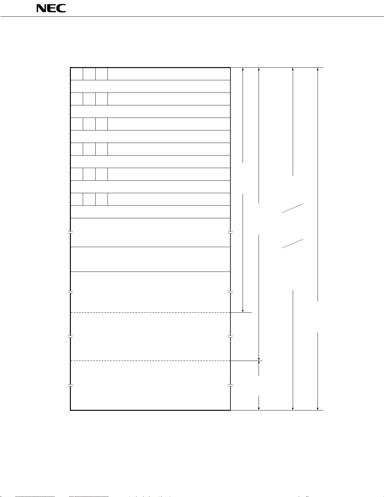
Page 41

µ
PD75104, 75106, 75108
Instruc- Mnetions monics Cyc- Area Conditions
Subroutine/
Stack
Control
(Cont‘d)
CALLF ! faddr 2 2 • µPD75104 *9
RET 1 3 • µPD75104
RETS 1 3+S • µPD75104 Unconditioned
RETI 1 3 • µPD75104
PUSH rp 1 1 (SP-1)(SP-2) ← rp, SP ← SP-2
POP rp 1 1 rp ← (SP+1)(SP), SP ← SP+2
Operand Bytes
BS 2 2 (SP-1) ← MBS, (SP-2) ← RBS,
BS 2 2 MBS ← (SP+1), RBS ← (SP),
Ma-
chine
les
Operation
(SP-4)(SP-1)(SP-2) ← PC11-0
(SP-3) ← MBE, RBE, 0, 0
PC11-0 ←0, faddr, SP ← SP-4
• µPD75106, 75108
(SP-4)(SP-1)(SP-2) ← PC11-0
(SP-3) ← MBE, RBE, 0, PC12
PC12-0 ← 00, faddr, SP ← SP-4
MBE, RBE, x, x ← (SP+1)
PC11-0 ← (SP)(SP+3)(SP+2)
SP ← SP+4
• µPD75106, 75108
MBE, RBE, x, PC12 ← (SP+1)
PC11-0 ← (SP)(SP+3)(SP+2)
SP ← SP+4
MBE, RBE, x, x ← (SP+1)
PC11-0 ← (SP)(SP+3)(SP+2)
SP ← SP+4,
• µPD75106, 75108
MBE, RBE, x, PC12 ← (SP+1)
PC11-0 ← (SP)(SP+3)(SP+2)
SP ← SP+4,
MBE, RBE, x, x ← (SP+1)
PC11-0 ← (SP)(SP+3)(SP+2)
PSW ← (SP+4)(SP+5), SP ← SP+6
• µPD75106, 75108
MBE, RBE, x, PC12 ← (SP+1)
PC11-0 ← (SP)(SP+3)(SP+2)
PSW ← (SP+4)(SP+5), SP ← SP+6
SP ← SP-2
SP ← SP+2
then skip unconditionally
then skip unconditionally
Addressing Skip
41
Page 42

µ
PD75104, 75106, 75108
Instruc- Mnetions monics Cyc- Area Conditions
Inter- EI 2 2 IME (IPS.3) ← 1
rupt IExxx 2 2 IExxx ← 1
Control DI 2 2 IME (IPS.3) ← 0
I/O IN* A, PORTn 2 2 A ← PORTn (n = 0-9, 12-14)
OUT* PORTn, A 2 2 PORTn ← A (n = 2-9, 12-14)
CPU HALT 2 2 Set HALT Mode (PCC.2 ← 1)
Control STOP 2 2 Set STOP Mode (PCC.3 ← 1)
NOP 1 1 No Operation
Special SEL RBn 2 2 RBS ← n (n = 0-3)
GETI taddr 1 3 • µPD75104 *10
Operand Bytes
IExxx 2 2 IExxx ← 0
XA, PORTn 2 2
PORTn, XA 2 2 PORTn+1, PORTn ← XA(n = 4, 6, 8, 12)
MBn 2 2 MBS ← n (n = 0, 1, 15)
Ma-
chine
les
XA
←
• Where TBR instruction,
PC11-0 ← (taddr)3-0+(taddr+1)
.........................................................
• Where TCALL instruction,
(SP-4)(SP-1)(SP-2) ← PC11-0
(SP-3) ← MBE, RBE, 0, 0
PC11-0 ← (taddr)3-0+(taddr+1)
SP ← SP-4
......................................................... .............................
• Except for TBR and TCALL Depends on
instructions, referenced
Instruction execution of instruction
(taddr)(taddr+1)
Operation
PORTn+1,PORTn
(n = 4, 6, 8, 12)
Addressing Skip
• µPD75106, 75108
• Where TBR instruction,
PC12-0 ← (taddr)4-0+(taddr+1)
.........................................................
• Where TCALL instruction,
(SP-4)(SP-1)(SP-2) ← PC11-0
(SP-3) ← MBE, RBE, 0, PC12
PC12-0 ← (taddr)4-0+(taddr+1)
SP ← SP-4
......................................................... .............................
• Except for TBR and TCALL Depends on
instructions, referenced
Instruction execution of instruction
(taddr)(taddr+1)
*: When executing the IN/OUT instruction, MBE = 0, or MBE = 1, and MBS = 15.
★
Remarks: TBR and TCALL instructions are assembler instructions for GETI instruction table definition.
42
Page 43

10. APPLICATION EXAMPLES
10.1 VTR SYSTEM CONTROLLER
µ
PD75104, 75106, 75108
Remote
controller
signal
receiver
Operation
mode LED
indicator
Servo
system
control
circuit
Motor
driver
circuit,
etc.
Highcurrent
output
PD75108
µ
System
controller/
tape counter/
remote controller/
remaining tape
computation
Comparator
input
12 V
Audio video system
control circuit
INT
INT
INT
Key
matrix
Sensor circuit
Exposure sensor
Tape start/end
sensor
SIO
Take-up reel pulse
Supply reel pulse
PD752
µ
××
timer/tuner/OSD
TunerFIP
On-screen
display
controller
MNOS
µ
PD6252
µ
PD6253
µ
PD6254
PWM output
10.2 VTR CAMERA
Operation
mode LED
indicator
Servo
system
control
circuit
Motor
plunger
driver
circuit,
etc.
Highcurrent
output
PD75108
µ
System control/
editing
function
INT
Comparator
input
INT
12 V
Audio video system
control circuit
Battery sensor
Key matrix
(including
message
input)
Reel pulse
Sensor circuit
Exposure sensor
Tape start/end
sensor
On-screen
display
controller
Powerdown
detector
43
Page 44

10.3 COMPACT DISC PLAYER
PD75108
µ
µ
PD75104, 75106, 75108
Servo
control
IC
Loading
control
circuit
Remote
controller
signal
receiver
SIO
INT
10.4 AUTOMOBILE APPLICATIONS (TRIP COMPUTER)
PD75108
µ
Vehicle speed
detection
Number of
revolutions
detection
Fuel
comsumption
Key position
Gear position
INT0
INT1
TI
SIO
Highcurrent
output
Display
driver
PD6300
µ
PD6323
µ
µ
PD6332
Key
matrix
LED
indication
Clock
Alarm
Average
speed
Arrival
time, etc.
44
Key input
Mode select
Numerical
input
TO
Buzzer
Page 45

10.5 PUSHBUTTON TELEPHONE
Hook switch
Transmitter/
receiver/
speaker
selector
µ
PD75104, 75106, 75108
Transmitter/
receiver
Communication
circuit
To main
equipment
LED
indicator
Key
matrix
Highcurrent
output
Data
receiver
circuit
Data
transmitter
circuit
µ
PD75108
TO
Filter
SIO
MPX
Call sound
µ
PD7228G
LCD
controller/
driver
Speaker
amplifier
Microphone
amplifier
Speaker
Microphone
LCD indicator
10.6 DISPLAY PAGER
Code ROM
Piezoelectric
buzzer
Filter
µ
PD75108
INT
TO
LCD controller/
driver
µ
PD7228/7229
Comparator
input
SIO
Highcurrent
output
RAM
µ
PD4464
Switch
LED indicator
LCD indicator
Battery
check
45
Page 46

10.7 PLAIN PAPER COPIER (PPC)
Motor/relay
driver
circuit
12 V
PD75108
µ
Highcurrent
output
µ
PD75104, 75106, 75108
LED indicator
Switch
Piezoelectric
buzzer
10.8 PRINTER CONTROLLER
Host machine
PD0 to PD7
STRB
BUSY
TO
Comparator
INT
input
PD75108
µ
Key matrix
Sensor circuit,
heater
temperature, toner
drum pressure, etc.
12 V
Motor
driver
control
circuit
46
TxD
Key matrix
SI
High
current
TO
Dot
matrix
head
driver
circuit
LED
Piezoelectric
buzzer
Page 47

11. MASK OPTION SELECTION
µ
PD75108 has the following mask options. Options to be built in can be selected.
(1) Pin
Pin Mask Option
P120 - P123
P130 - P133 Pull-down resistor can be built in bitwise.
P140 - P143
(2) Power-ON reset generation circuit, power-ON flag (PONF)
One from the following three ways can be selected.
µ
PD75104, 75106, 75108
Switching Selection
(Refer to Fig. 8-1.)
SWA SWB
ON ON Provided Provided Generates automatically
ON OFF Provided Provided Not generates autoamtically
OFF OFF Not provided Not provided —
Power-On Reset Power-On Flag Internal Reset Signal
Generation Circuit (PONF) (RES)
47
Page 48

µ
PD75104, 75106, 75108
12. ELECTRICAL SPECIFICATIONS
ABSOLUTE MAXIMUM RATINGS (Ta = 25°C)
Parameter Symbol Conditions Ratings Unit
Supply Voltage VDD -0.3 to +7.0 V
VI1 Other than ports 12, 13, 14 -0.3 to VDD+0.3 V
Input Voltage VI2*1Ports 12 to 14 w/pull-up -0.3 to VDD+0.3
Output Voltage VO -0.3 to VDD+0.3 V
High-Level Output IOH 1 pin -15 mA
Current
Low-Level Output IOL*21 pin Peak 30 mA
Current rms 15 mA
Operating Temperature Topt -40 to +85 °C
Storage Temperature Tstg -65 to +150 °C
All pins -30 mA
Total of ports 0, 2 to 4, 12 to 14 Peak 100 mA
Total of ports 5 to 9 Peak 100 mA
resistor
Open drain -0.3 to +13 V
rms 60 mA
rms 60 mA
V
*1: The power supply impedance (pull-up resistance) must be 50 kΩ or higher when a voltage higher than
10 V is applied to ports 12, 13, and 14.
2: rms = Peak value x √Duty
48
Page 49

OSCILLATOR CIRCUIT CHARACTERISTICS
a = -40 to +85°C, VDD = 2.7 to 6.0 V)
(T
µ
PD75104, 75106, 75108
Oscillator
Ceramic Oscillation VDD = Oscillation
Crystal Oscillation
External Clock X1 input frequency
Recommended
Constants
X1 X2
C1 C2
X1 X2
C1 C2
X1 X2
µ
PD74HCU04
Item Conditions MIN. TYP. MAX. Unit
3
frequency(fXX)*
Oscillation stabiliza- After VDD come to
tion time*
frequency (fXX)*
Oscillation stabiliza- VDD = 4.5 to 6.0 V 10 ms
tion time*
1
(fX)*
X1 input high-,
low-level widths
(tXH, tXL) 100 250 ns
1
voltage range
2
2
MIN. of oscillation
voltage range
1
2.0 5.0 MHz
2.0 4.19 5.0 MHz
2.0 5.0 MHz
*
4ms
3
*
30 ms
3
*
*1: The oscillation frequency and X1 input frequency are indicated only to express the characteristics
of the oscillator circuit. For instruction execution time, refer to AC Characteristics.
2: Time required for oscillation to stabilize after V
DD has come to MIN. of oscillation volrage range
or the STOP mode has been released.
3: When the oscillation frequency is 4.19 MHz < fx ≤ 5.0 MHz, do not select PCC = 0011 as the
µ
instruction execution time: otherwise, one machine cycle is set to less than 0.95
of the rated minimum value of 0.95
µ
s.
s, falling short
★
Note: When using the oscillation circuit of the system clock, wire the portion enclosed in dotted line
in the figures as follows to avoid adverse influences on the wiring capacity:
• Keep the wiring length as short as possible.
• Do not cross the wiring over the other signal lines. Also, do not route the wiring in the vicinity
of lines through which a high alternating current flows.
• Always keep the ground point of the capacitor of the osccillator circuit at the same potential
as V
SS. Do not connect the ground pattern through which a high current flows.
• Do not extract signals from the oscillation circuit.
★
49
Page 50

µ
PD75104, 75106, 75108
RECOMMENDED OSCILLATOR CIRCUITS CONSTANTS
RECOMMENDED CERAMIC OSCILLATORS
External Oscillation
Manufacturer Product Name
CSA 2.00MG 30 30 2.7 6.0
Murata Mfg. CSA 4.19MG 30 30 3.0 6.0
Co., Ltd. CSA 4.19MGU 30 30 2.7 6.0
CST 4.19T Provided Provided 3.0 6.0
KBR-2.0MS 100 100 3.0 6.0
Kyoto Ceramic KBR-4.0MS 33 33 3.0 6.0
Co., Ltd. KBR-4.19MS 33 33 3.0 6.0
Capacitance (pF) Voltage Range (V)
C1 C2 MIN. MAX.
KBR-4.9152M 33 33 3.0 6.0
RECOMMENDED CRYSTAL OSCILLATOR
Manufacturer Product Name
Kinseki HC-49/U 22 22 2.7 6.0
External Oscillation
Capacitance (pF) Voltage Range (V)
C1 C2 MIN. MAX.
50
Page 51

µ
PD75104, 75106, 75108
DC CHARACTERISTICS (Ta = -40 to +85°C, VDD = 2.7 to 6.0 V)
Item Symbol Conditions MIN. TYP. MAX. Unit
VIH1 Other than below 0.7VDD VDD V
High-Level VIH2 Ports 0, 1, TI0, 1, RESET 0.8 VDD VDD V
Input Voltage Pull-up resistor 0.7 VDD VDD V
Low-Level Input Voltage VIL2 Ports 0, 1, TI0, 1, RESET 0 0.2 VDD V
High-Level Output Voltage VOH
Low-Level Output Voltage VOL
High-Level Input Leakage
Current
VIH3 Ports 12 to 14
Open drain 0.7 VDD 12 V
VIH4 X1, X2 VDD-0.5 VDD V
VIL1 Other than below 0 0.3 VDD V
VIL3 X1, X2 0 0.4 V
VDD = 4.5 to 6.0 V,IOH = -1 mA VDD-1.0 V
IOH = -100 µAVDD-0.5 V
VDD = Ports 0, 2 to 9, IOL = 15 mA 0.35 2.0 V
4.5 to 6.0 V Ports 12 to 14, IOL = 10 mA 0.35 2.0 V
VDD = 4.5 to 6.0 V, IOL = 1.6 mA 0.4 V
IOL = 400 µA 0.5 V
ILIH1 Other than below 3
ILIH2 X1,X2 20
ILIH3 VIN = 12 V Ports 12 to 14 (open drain) 20
VIN = VDD
µ
A
µ
A
µ
A
Low-Level ILIL1 Other than X1, X2 –3
Input Leakage Current ILIL2 X1, X2 –20
High-Level ILOH1 VOUT = VDD Other than below 3
Output Leakage Current ILOH2 VOUT = 12 V Ports 12 to 14 (open drain) 20
Low-Level Output ILOL VOUT = 0 V –3
Leakage Current
Internal Pull-Up Resistor*1RL Ports 12 to 14
IDD1
Supply Current*
1
IDD2
IDD3 STOP mode, VDD = 3 V±10% 0.1 10
VIN = 0 V
VDD = 5 V±10% 15 40 70 kΩ
10 80 kΩ
4.19MHz VDD = 5 V±10%*
crystal VDD = 3 V±10%*
oscillator HALT VDD = 5 V±10% 600 1800
C1 = C2 = 22pF mode VDD = 3±10% 200 600
2
3
39mA
0.55 1.5 mA
µ
A
µ
A
µ
A
µ
A
µ
A
µ
A
µ
A
µ
A
*1: The current flowing into the internal pull-up resistor, power-ON reset circuit (mask option), and comparator
circuit is not included.
2: When the high-speed mode is set by setting the processor clock control register (PCC) to 0011.
3: When the low-speed mode is set by setting the PCC to 0000.
51
Page 52

µ
PD75104, 75106, 75108
CAPACITANCE (Ta = 25°C, VDD = 0 V)
Parameter Symbol Conditions MIN. TYP. MAX. Unit
Input Capacitance CIN f = 1 MHz 15 pF
Output Capacitance COUT Pins other than thosemeasured are at 0 V 15 pF
Input/Output CIO 15 pF
Capacitance
COMPARATOR CHARACTERISTICS (Ta = -40 to +85°C, VDD = 4.5 to 6.0 V)
Parameter Symbol Conditions MIN. TYP. MAX. Unit
Comparison Accuracy VACOMP ±100 mV
Threshold Voltage VTH 0VDD V
PTH Input voltage VIPTH 0VDD V
Comparator circuit PTHM7 is set to “1” 1 mA
current dissipation
POWER-ON RESET CIRCUIT CHARACTERISTICS (MASK OPTION) (Ta = -40 to +85°C)
Parameter Symbol Conditions MIN. TYP. MAX. Unit
Power-On Reset
High-Level VDDH 4.5 6.0 V
Operating Voltage
Power-On Reset
Low-Level VDDL 0 0.2 V
Operating Voltage
Supply Voltage tr 10 *
1
µ
s
Rise Time
Supply Voltage toff 1s
Off Time
Power-On Reset Circuit IDDPR VDD = 5 V± 10% 10 100
Current Dissipation*
2
VDD = 2.5 V 2 20
µ
A
µ
A
*1: 217/fXX (31.3 ms at fXX = 4.19 MHz)
2: Current flowing when power-ON reset circuit or power-ON Flag is incorporeated.
V
V
DD
DDH
V
DDL
Note: Apply power gradually and smoothly.
52
t
off
t
r
Page 53

µ
PD75104, 75106, 75108
AC CHARACTERISTICS (Ta = -40 to +85°C, VDD = 2.7 to 6.0 V)
Parameter Symbol Conditions MIN. TYP. MAX. Unit
CPU Clock Cycle Time*
(Minimum Instruction
Execution Time = 1
Machine Cycle)
TI0, TI1 Input Frequency fTI
TI0, TI1 Input High-/
Low-Level Width
SCK Cycle Time tKCY
SCK High-/Low-Level
Width
SI Setup Time tSIK 100 ns
(vs. SCK↑)
SI Hold Time tKSI 400 ns
(vs. SCK↑)
SCK ↓→ SO Output
delay Time
INT0 to 4 tINTH,
High-/Low-Level Width tINTL
RESET Low-Level Width tRSL 5
tCY
tTIH,VDD = 4.5 to 6.0 V 0.48
t
TIL
tKH,
tKL
tKSO
VDD = 4.5 to 6.0 V 0.95 32
3.8 32
VDD = 4.5 to 6.0 V 0 1 MHz
0 275 kHz
1.8
VDD = 4.5 to 6.0 V Input 0.8
Output 0.95
Input 3.2
Output 3.8
VDD = 4.5 to 6.0 V Input 0.4
Output tKCY/2-50 ns
Input 1.6
Output
VDD = 4.5 to 6.0 V 300 ns
tKCY/2-150
1000 ns
5
µ
µ
µ
µ
µ
µ
µ
µ
µ
µ
ns
µ
µ
s
s
s
s
s
s
s
s
s
s
s
s
*: The cycle time of the CPU clock (Φ) is
determined by the input frequency of
the ceramic or crystal oscillator circuit
and the set value of the processor clock
control register. The t
CY vs. VDD charac-
teristics are as shown on the right.
tCY vs. V
DD
40
32
7
6
5
4
3
µ
[ s]
CY
t
2
1
0.5
0123 456
DD
[V]
V
Operation
guaranteed
range
53
Page 54

µ
PD75104, 75106, 75108
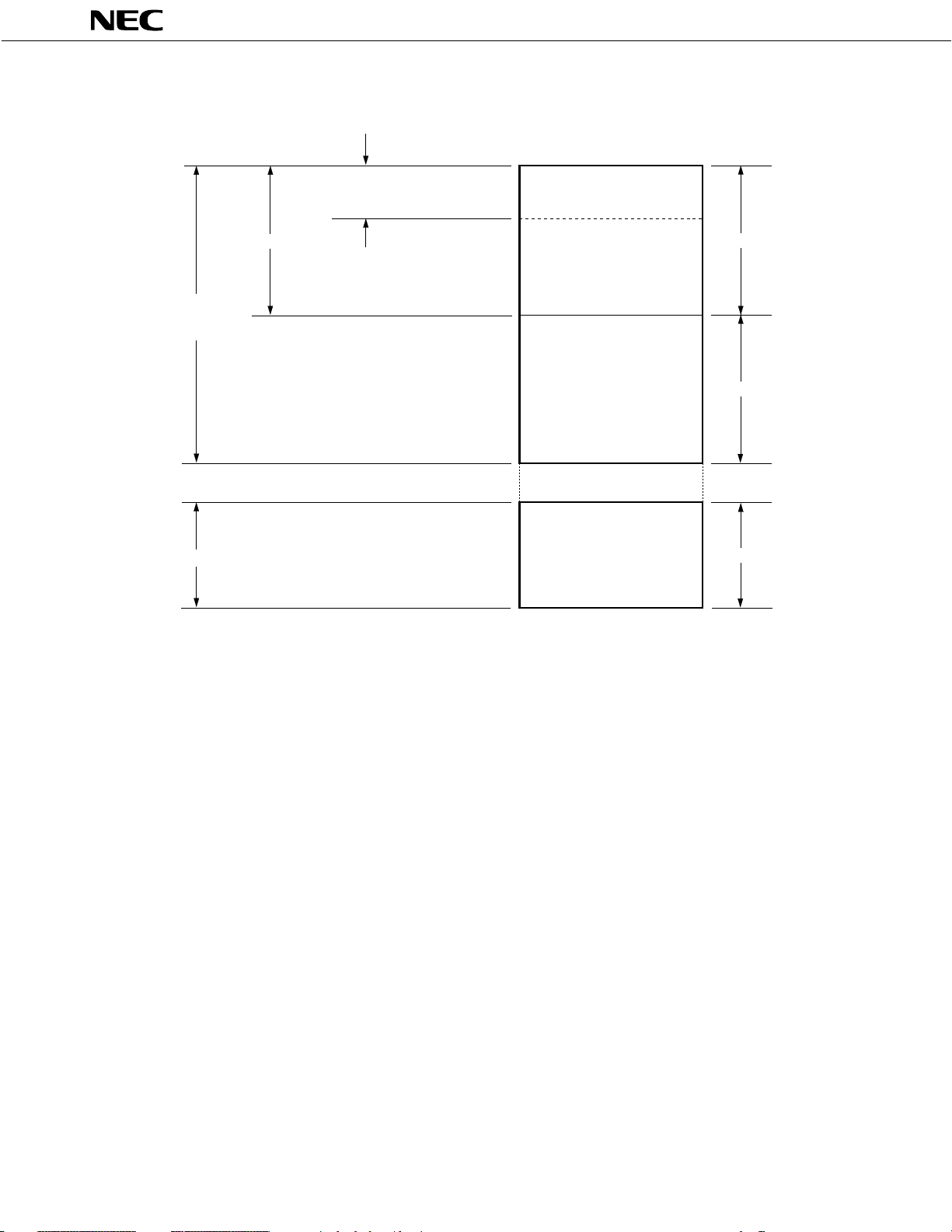
AC TIMING MEASURING POINTS (excluding Ports 0, 1, TI0, TI1, X1, X2, and RESET)
0.7 V
0.3 V
DD
DD
Measuring
points
0.7 V
0.3 V
DD
DD
CLOCK TIMING
1/f
X
t
XL
t
XH
TI TIMING
TI0, TI1
X1 input
V
DD
–0.5
0.4
1/f
TI
t
TIL
t
TIH
V
DD
0.8
0.2
V
DD
54
Page 55

SERIAL TRANSFER TIMING
SCK
SI
µ
PD75104, 75106, 75108
t
KCY
t
KL
t
SIK
Input data
KSO
t
t
KH
0.8 V
DD
0.2 V
DD
t
KSI
0.8 V
DD
0.2 V
DD
SO
INTERRUPT INPUT TIMING
INT0 to 4
RESET INPUT TIMING
RESET
Output data
tINTL tINTH
0.8 V
DD
0.2 V
DD
t
RSL
0.2 V
DD
55
Page 56

µ
PD75104, 75106, 75108
LOW-VOLTAGE DATA RETENTION CHARACTERISTICS OF DATA MEMORY IN STOP MODE
a = –40 to +85°C)
(T
Parameter Symbol Conditions MIN. TYP. MAX. Unit
Data Retention Supply VDDDR
Voltage
Data Retention Supply IDDDR VDDDR = 2.0 V
Current*
1
2.0 6.0 V
0.1 10
Release Signal Set Time tSREL 0
Oscillation Stabilization tWAIT Released by RESET 217/fX ms
Wait Time*
2
Released by interrupt request *
3
*1: The current flowing through internal pull-up resistor, power-ON reset circuit (mask option), and
comparator circuit is not included
2: The oscillation stabilization wait time is the time during which the CPU is stopped to prevent
unstable operation when oscillation is started.
3: Depends on the setting of the basic interval timer mode register (BTM) as follows:
BTM3 BTM2 BTM1 BTM0 Wait time ( ): fXX = 4.19 MHz
–0002
–0112
–1012
–1112
20
/fXX (approx. 250 ms)
17
/fXX (approx. 31.3 ms)
15
/fXX (approx. 7.82 ms)
13
/fXX (approx. 1.95 ms)
µ
µ
ms
A
s
DATA RETENTION TIMING (releasing STOP mode by RESET)
Internal reset operation
HALT mode
STOP mode
Data retention mode
DD
V
V
DDDR
t
SREL
STOP instruction
execution
RESET
t
WAIT
DATA RETENTION TIMING (standby release signal: releasing STOP mode by interrupt)
HALT mode
STOP mode
Data retention mode
Operation
mode
Operation
mode
56
V
DD
STOP instruction execution
Standby release signal
(interrupt request)
V
DDDR
t
SREL
t
WAIT
Page 57

13. CHARACTERISTIC DATA
5000
µ
PD75104, 75106, 75108
I vs. V Characteristics (crystal oscillation)
DD DD
High-speed mode [0011]
Medium-speed mode [0010]
Low-speed mode [0000]
a
(T = 25˚C)
1000
500
µ
100
DD
50
10
Supply current I [ A]
5
Figure in [ ] indicate
set values of PCC.
1
0.5
X1 X2
22 pF
0123 456
Supply voltage V [V]
I vs. f Characteristics (crystal oscillation)
DD XX
DD
HALT mode [0100]
STOP mode [1000]
When power-ON
reset circuit and
power-ON flag are
incorporated.
Crystal
oscillation
4.194304 MHz
22 pF
(V = 5.0 V, T = 25˚C)
DD
a
3.0
Figure in [ ] indicate
set values of PCC.
X1 X2
2.5
C
1
C
2
2.0
DD
1.5
Supply current I [mA]
1.0
0.5
0
0123 5
4
f [MHz]
XX
High-speed mode [0011]
Medium-speed mode [0010]
Low-speed mode [0000]
HALT mode [0100]
57
Page 58

5000
µ
PD75104, 75106, 75108
I vs. V Characteristics (ceramic oscillation)
DD DD
a
(T = 25˚C)
High-speed mode [0011]
Medium-speed mode [0010]
Low-speed mode [0000]
1000
500
µ
100
DD
50
10
Supply current I [ A]
5
Figure in [ ] indicate
set values of PCC.
1
0.5
X1 X2
30 pF
30 pF
0123456
Supply voltage V [V]
I vs. f Characteristics (ceramic oscillation)
XXDD
HALT mode [0100]
STOP mode [1000]
When power-ON
reset circuit and
power-ON flag are
incorporated.
Ceramic
oscillation
4.19 MHz
DD
(V = 5.0 V, T = 25˚C)
DD
a
3.0
Figure in [ ] indicate
set values of PCC.
X1 X2
2.5
CC
12
2.0
DD
1.5
Supply current I [mA]
1.0
0.5
0
0123 5
4
XX
f [MHz]
High-speed mode [0011]
Medium-speed mode [0010]
Low-speed mode [0000]
HALT mode [0100]
58
Page 59

I vs. f Characteristics (external clock)
DD X
(V = 5.0 V, T = 25˚C)
DD
µ
PD75104, 75106, 75108
a
3.0
Figures in [ ] indicate
set values of PCC.
X1 X2
2.5
PD74HCU04
µ
2.0
µ
DD
1.5
Supply current I [ A]
1.0
0.5
0
012345
f [MHz]
X
f vs. V Characteristics
DDTI
High-speed mode [0011]
Medium-speed mode [0010]
Low-speed mode [0000]
HALT mode [0100]
1000
TI
500
Operation guaranteed
TIn input frequency f [kHz]
range
100
50
012345
V [V]
DD
67
59
Page 60

µ
PD75104, 75106, 75108
V vs. I (Ports 0 and 2 to 9) Characteristics
OL OL
V = 5 V
V = 6 V
30
OL
DD
DD
V = 4 V
DD
V = 3 V
DD
20
10
Low-level output current of port 0 and 2 to 9 I [mA]
0
01234
OL
V [V]
V vs. I (Ports 12 to 14) Characteristics
OL OL
30
OL
V = 6 VDDV = 5 V
DD
DD
V = 4 V
20
V = 3 V
DD
10
60
Low-level output current of ports 12 to 14 I [mA]
0
01234
V [V]
OL
Page 61

V vs. I (Ports 0 and 2 to 9) Characteristics
OH OH
–15
OH
V = 6 VDDV = 5 V
DD
–10
–5
High-level output current of port 0 and 2 to 9 I [mA]
V = 3 V
DD
µ
PD75104, 75106, 75108
V = 4 V
DD
0
01234
DD OH
V - V [V]
Remarks: Unless otherwise specified, all the characteristic data shown are reference values.
61
Page 62

14. PACKAGE DRAWINGS
64 PIN PLASTIC SHRINK DIP (750 mil)
64 33
A
µ
PD75104, 75106, 75108
321
K
I
J
H
G
NOTE
Each lead centerline is located within 0.17 mm (0.007 inch) of
1)
its true position (T.P.) at maximum material condition.
Item "K" to center of leads when formed parallel.2)
F
M
D
N
L
B
C
ITEM MILLIMETERS INCHES
A
B
C
D
F
G
H
I
J
K
L
M
N
R
M
58.68 MAX.
1.78 MAX.
1.778 (T.P.)
0.50±0.10
0.9 MIN.
3.2±0.3
0.51 MIN.
4.31 MAX.
5.08 MAX.
19.05 (T.P.)
17.0
+0.10
0.25
–0.05
0.17
0~15°
2.311 MAX.
0.070 MAX.
0.070 (T.P.)
0.020
0.035 MIN.
0.126±0.012
0.020 MIN.
0.170 MAX.
0.200 MAX.
0.750 (T.P.)
0.669
0.010
0.007
0~15°
P64C-70-750A,C-1
+0.004
–0.005
+0.004
–0.003
R
62
Page 63

64 PIN PLASTIC QFP (14×20)
A
B
µ
PD75104, 75106, 75108
52
64
51
1
33
19
32
20
F
G
H
M
I
P
N
NOTE
Each lead centerline is located within 0.20 mm (0.008 inch) of
its true position (T.P.) at maximum material condition.
detail of lead end
C D
S
Q
R
J
K
M
L
ITEM MILLIMETERS INCHES
A
23.6±0.4
B
20.0±0.2
C
14.0±0.2
D 17.6±0.4 0.693±0.016
F 1.0 0.039
G 1.0 0.039
H 0.40±0.10 0.016
I 0.20 0.008
J 1.0 (T.P.) 0.039 (T.P)
K 1.8±0.2 0.071
L 0.8±0.2 0.031
M 0.15 0.006
N 0.10 0.004
P 2.7 0.106
Q 0.1±0.1 0.004±0.004
R 5°±5° 5°±5°
S 3.0 MAX. 0.119 MAX.
+0.10
–0.05
P64GF-100-3B8,3BE,3BR-2
0.929±0.016
+0.008
0.795
–0.009
+0.009
0.551
–0.008
+0.004
–0.005
+0.008
–0.009
+0.009
–0.008
+0.004
–0.003
63
Page 64

Page 65

µ
PD75104, 75106, 75108
15. RECOMMENDED SOLDERING CONDITIONS
It is recommended that µPD75104, 75106, and 75108 be soldered under the following conditions.
For details on the recommended soldering conditions, refer to Information Document "Semiconductor
Devices Mounting Manual" (IEI-616).
For other soldering methods and conditions, please consult NEC.
Table 15-1 Soldering Conditions of Surface Mount Type
µ
PD75108GF - xxx - 3BE: 64-pin plastic QFP (14 x 20 mm)
Soldering Method Soldering Conditions
Infrared Reflow Package peak temperature: 230°C, time: 30 seconds max. IR30-00-1
(210°C min.), number of times: 1
VPS Package peak temperature: 215°C, time: 40 seconds max. VP15-00-1
(200°C min.), number of times: 1
Wave Soldering Soldering bath temperature: 260°C max., time: 10 seconds WS60-00-1
max., number of times: 1,
pre-heating temperature: 120°C max. (package surface
temperature)
Pin Partial Heating Pin temperature: 300°C max., —
time: 3 seconds max. (per side)
Symbol for Recommended
Condition
Caution: Do not use two or more soldering methods in combination (except the pin partial heating
method).
Table 15-2 Soldering Conditions of Through-Hole Type
µ
PD75108CW - xxx : 64-pin plastic shrink DIP (750 mil)
Soldering Method Soldering Conditions
Wave Soldering Soldering bath temperature: 260°C max., Time: 10 seconds max.
(Only for lead part)
Pin Partial Heating Pin temperature: 260°C max., Time: 10 seconds max.
Caution: The wave soldering must be performed at the lead part only. Note that the solder must not be
directly contacted to the package body.
65
Page 66

66
APPENDIX A. FUNCTIONAL DIFFERENCES AMONG PRODUCTS IN PD751XX SERIES
Item PD75104
ROM Configuration Mask ROM PROM
ROM (Bits)
RAM (Bits)
Instruction Set High-end (Only PD75104 and 75104A are not provided with BR!addr instruction.)
Total
I/O
Lines
Power-ON
Reset Circuit
Power-ON Flag
Operating
Voltage Range
Minimum
Instruction
Execution
Time
Pin Connections Depends on package
Package
I/O
Input
µ
000H-FFFH 0000H-177FH 0000H-1F7FH 0000H-2F7FH 0000H-3F7FH 000H-FFFH 0000H-1F7FH 0000H-1F7FH 0000H-2F7FH 0000H-3F7FH 0000H-1F7FH 0000H-3F7FH
4096 × 8 6016 × 8 8064 × 8 12160 × 8 16256 × 8 4096 × 8 8064 × 8 8064 × 8 12160 × 8 16256 × 8 8064 × 8 16256 × 8
(Bank 0: 256 × 4)
(Bank 1: 64 × 4)
• 64-pin plastic shrink DIP (750 mil)
• 64-pin plastic QFP (14 × 20 mm)
µ
PD75106
320 × 4
µ
• CMOS I/O: 32
• +12 V open-drain output: 12
(pull-up resistor as mask option)
LED direct drive: 44
µ
PD75108
• CMOS input: 10
• Comparator input: 4
PD75112µPD75116µPD75104AµPD75108AµPD75108FµPD75112FµPD75116FµPD75P108BµPD75P116
512 × 4
(Bank 0: 256 × 4)
(Bank 1: 256 × 4)
Provided (mask option)
2.7 to 6.0 V
0.95 s (at 5 V)
µ
3 s (at 3 V)
µ
• 64-pin plastic shrink DIP
(750 mil)
• 64-pin plastic QFP (14 × 20
mm)
320 × 4
(Bank 0:
256 × 4)
(Bank 1:
64 × 4)
• CMOS I/O: 32
(pull-up resistor as mask
option: 24)
• +12 V open-drain output: 12
(pull-up resistor as mask
option)
LED direct drive: 44
• CMOS input: 10
(pull-up resistor as mask
option: 4)
• Comparator input: 44
• 64-pin
plastic QFP
(14 × 14
mm)
512 × 4
(Bank 0:
256 × 4)
(Bank 1:
256 × 4)
58
plastic QFP
(14 × 14
mm)
• 64-pin
plastic QFP
(14 × 14
mm)
µ
512 × 4
(Bank 0: 256 × 4)
(Bank 1: 256 × 4)
High end
• CMOS I/O: 32
• +10 V open-drain output: 12
(pull-up resistor as mask option)
LED direct drive: 44
• CMOS input: 10
• Comparator input: 4
None
2.7 to 5.0 V (T
2.8 to 5.0 V (T
0.95 s (at 4.5 V to 5.0 V)
Depends on package. Only PD75P108, and 75P116 are provided with
V
PP
pin.
• 64-pin plastic QFP (14 × 20 mm)• 64-pin
a
= -40 to +50°C)
a
= -40 to +60°C)
µ
µ
1.91 s (at 3 V)
µ
• CMOS I/O: 32
• +12 V open-drain output:
12
LED direct drive: 44
2.7 to 6.0 V 5 V ± 10%
µ
0.95 s
(at 5 V)
µ
3 s
(at 3 V)
• 64-pin
plastic
shrink DIP
(750 mil)
• 64-pin
ceramic
shrink DIP
(w/window)
• 64-pin
plastic QFP
(14 × 20
mm)
• 64-pin
• 64-pin
µ
µ
0.95 s
(at 5 V)
plastic
shrink DIP
(750 mil)
plastic QFP
(14 × 20
mm)
µ
PD75104, 75106, 75108
Page 67

µ
PD75104, 75106, 75108
APPENDIX B. DEVELOPMENT TOOLS
The following development support tools are readily available to support development of systems using
µ
PD75108:
Hardware IE-75000-R*
IE-75001-R
IE-75000-R-EM*
EP-75108CW-R Emulation prove for µPD75108CW
EP-75108GF-R Emulation prove for µPD75108GF. It is provided with a 64-pin conversion
PG-1500 PROM programmer
PA-75P108CW PROM programmer adapter for µPD75P108BCW and 75P108BDW.
PA-75P116GF Programmer adapter for µPD75P108BGF.
Software IE Control Program
PG-1500 Controller
RA75X Relocatable
Assembler
1
2
EV-9200G-64
In-circuit emulator for 75X series
Emulation board for IE-75000-R and IE-75001-R
socket, EV-9200G-64
It is connected to PG-1500.
It is connected to PG-1500.
Host machine
PC-9800 series (MS-DOSTM Ver.3.30 to Ver.5.00A*3)
IBM PC/ATTM (PC DOSTM Ver.3.1)
*1: Maintenance product
2: Not provided with IE-75001-R.
3: Ver.5.00/5.00A has a task swap function, but this function cannot be used with this function.
Remarks:
For development tools from other companies, refer to 75X Series Selection Guide (IF-151).
67
Page 68

APPENDIX C. RELATED DOCUMENTS
PD75104, 75106, 75108
68
Page 69

µ
PD75104, 75106, 75108
GENERAL NOTES ON CMOS DEVICES
1 STATIC ELECTRICITY (ALL MOS DEVICES)
Exercise care so that MOS devices are not adversely influenced by static electricity while being
handled.
The insulation of the gates of the MOS device may be destroyed by a strong static charge.
Therefore, when transporting or storing the MOS device, use a conductive tray, magazine case,
or conductive buffer materials, or the metal case NEC uses for packaging and shipment, and use
grounding when assembling the MOS device system. Do not leave the MOS device on a plastic
plate and do not touch the pins of the device.
Handle boards on which MOS devices are mounted similarly .
2 PROCESSING OF UNUSED PINS (CMOS DEVICES ONLY)
Fix the input level of CMOS devices.
Unlike bipolar or NMOS devices, if a CMOS device is operated with nothing connected to its
input pin, intermediate level input may be generated due to noise, and an inrush current may flow
through the device, causing the device to malfunction. Therefore, fix the input level of the device
by using a pull-down or pull-up resistor. If there is a possibility that an unused pin serves as an
output pin (whose timing is not specified), each pin should be connected to V
a resistor.
Refer to “Processing of Unused Pins” in the documents of each devices.
DD or GND through
3 STATUS BEFORE INITIALIZATION (ALL MOS DEVICES)
The initial status of MOS devices is undefined upon power application.
Since the characteristics of an MOS device are determined by the quantity of injection at the
molecular level, the initial status of the device is not controlled during the production process. The
output status of pins, I/O setting, and register contents upon power application are not guaranteed.
However, the items defined for reset operation and mode setting are subject to guarantee after
the respective operations have been executed.
When using a device with a reset function, be sure to reset the device after power application.
69
Page 70

[MEMO]
µ
PD75104, 75106, 75108
No part of this document may be copied or reproduced in any form or by any means without the prior
written consent of NEC Corporation. NEC Corporation assumes no responsibility for any errors which
may appear in this document.
NEC Corporation does not assume any liability for infringement of patents, copyrights or other
intellectual property rights of third parties b y or arising from use of a device described herein or any
other liability arising from use of such device. No license, either express, implied or otherwise, is granted
under any patents, copyrights or other intellectual property rights of NEC Corporation or others.
The devices listed in this document are not suitable for uses in aerospace equipment, submarine cables,
nuclear reactor control systems and life support systems. If customers intend to use NEC devices for
above applications or they intend to use "Standard" quality grade NEC devices for the applications not
intended by NEC, please contact our sales people in advance.
Application examples recommended by NEC Corporation
Standard:
Special: Automotive and Transportation equipment, Traffic control systems, Antidisaster systems,
MS-DOS is a trademark of Microsoft Corporation.
PC DOS and PC/AT are trademarks of IBM Corporation.
Computer, Office equipment, Communication equipment, Test and Measurement equipment,
Machine tools, Industrial robots, Audio and Visual equipment, Other consumer products, etc.
Anticrime system, etc.
M4 92.6
70
Page 71

This datasheet has been downloaded from:
www.DatasheetCatalog.com
Datasheets for electronic components.
 Loading...